WO2022220176A1 - 電子素子収容用パッケージ及び電子装置 - Google Patents
電子素子収容用パッケージ及び電子装置 Download PDFInfo
- Publication number
- WO2022220176A1 WO2022220176A1 PCT/JP2022/017091 JP2022017091W WO2022220176A1 WO 2022220176 A1 WO2022220176 A1 WO 2022220176A1 JP 2022017091 W JP2022017091 W JP 2022017091W WO 2022220176 A1 WO2022220176 A1 WO 2022220176A1
- Authority
- WO
- WIPO (PCT)
- Prior art keywords
- section
- conductor
- signal
- signal conductor
- width
- Prior art date
- Legal status (The legal status is an assumption and is not a legal conclusion. Google has not performed a legal analysis and makes no representation as to the accuracy of the status listed.)
- Ceased
Links
Images


Classifications
-
- H—ELECTRICITY
- H01—ELECTRIC ELEMENTS
- H01P—WAVEGUIDES; RESONATORS, LINES, OR OTHER DEVICES OF THE WAVEGUIDE TYPE
- H01P5/00—Coupling devices of the waveguide type
- H01P5/08—Coupling devices of the waveguide type for linking dissimilar lines or devices
- H01P5/085—Coaxial-line/strip-line transitions
-
- H—ELECTRICITY
- H01—ELECTRIC ELEMENTS
- H01S—DEVICES USING THE PROCESS OF LIGHT AMPLIFICATION BY STIMULATED EMISSION OF RADIATION [LASER] TO AMPLIFY OR GENERATE LIGHT; DEVICES USING STIMULATED EMISSION OF ELECTROMAGNETIC RADIATION IN WAVE RANGES OTHER THAN OPTICAL
- H01S5/00—Semiconductor lasers
- H01S5/02—Structural details or components not essential to laser action
- H01S5/022—Mountings; Housings
-
- H—ELECTRICITY
- H01—ELECTRIC ELEMENTS
- H01P—WAVEGUIDES; RESONATORS, LINES, OR OTHER DEVICES OF THE WAVEGUIDE TYPE
- H01P3/00—Waveguides; Transmission lines of the waveguide type
- H01P3/02—Waveguides; Transmission lines of the waveguide type with two longitudinal conductors
- H01P3/06—Coaxial lines
Definitions
- the present disclosure relates to an electronic element housing package and an electronic device.
- Japanese Patent Laying-Open No. 2007-123950 discloses a high-frequency signal converter including a coaxial line positioned on a wall and a flat substrate connected to the coaxial line on the side of the wall.
- the electronic device housing package includes: a base body having a wall and an accommodating portion surrounded by the wall; a coaxial line positioned on the wall; a signal line connected to the coaxial line on the side of the wall, the coaxial line has a pin terminal projecting from the wall,
- the signal line includes an insulating plate having a first surface and a second surface located opposite to the first surface, a signal conductor located on the first surface and connected to the pin terminal, and the signal including a first ground conductor located on the first surface with the conductor sandwiched therebetween, and a second ground conductor located on the second surface;
- the signal line has a first section, a second section and a third section from the coaxial line side, the width of the signal conductor in the second section is constant, is equal to or less than the width of the signal conductor in the first section, and is wider than the width of the signal conductor in the central portion of the third section; In the second section, the spacing between the signal conductor and the first ground conductor is constant, narrower than
- the second section is located on the opposite side of the coaxial line from the position where the tip portions of the pin terminals overlap when viewed from the direction perpendicular to the first surface, and is located at the distance H between the signal conductor and the second ground conductor. It is a section having a length of 1/3 to 3/2 times.
- An electronic device includes: the electronic element housing package; an electronic element housed in the electronic element housing package; Prepare.
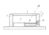
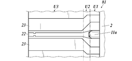
- FIG. 1 is a cross-sectional view showing an electronic element housing package and an electronic device according to an embodiment of the present disclosure
- FIG. 1 is a plan view showing an electronic device housing package and an electronic device according to an embodiment of the present disclosure
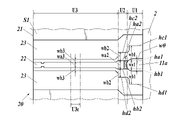
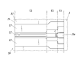
- FIG. It is a cross-sectional perspective view which shows the part of the transmission line of the package for electronic element accommodation of embodiment.
- It is a top view which shows the transmission line of embodiment.
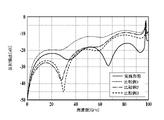
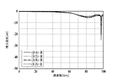
- 5 is a graph showing reflection characteristics of transmission lines of the embodiment and Comparative Examples 1 to 3.
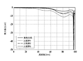
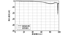
- FIG. 5 is a graph showing transmission characteristics of transmission lines of the embodiment and Comparative Examples 1 to 3
- 3 is a plan view showing a transmission line of Comparative Example 1;
- FIG. 8 is a plan view showing a transmission line of Comparative Example 2;
- FIG. 11 is a plan view showing a transmission line of Comparative Example 3;
- FIG. 4 is a plan view showing a first example of a transmission line of an embodiment in which the length of the second section is changed;
- FIG. 10 is a plan view showing a second example of the transmission line of the embodiment in which the length of the second section is changed;
- 9 is a graph showing reflection characteristics of a transmission line with a shortened second section;
- 9 is a graph showing transmission characteristics of a transmission line with a shortened second section;
- 7 is a graph showing reflection characteristics of a transmission line with a longer second section;
- 7 is a graph showing transmission characteristics of a transmission line with a longer second section;
- It is a figure which shows the top view which shows the modification 1 of the transmission line of embodiment.
- 9 is a graph showing reflection characteristics of Modification 1 of the transmission line of the embodiment; 9 is a graph showing transmission characteristics of Modification 1 of the transmission line of the embodiment; It is a cross-sectional perspective view which shows the modification 2 of the transmission line of embodiment. 9 is a graph showing reflection characteristics of Modification 2 of the transmission line of the embodiment; 9 is a graph showing transmission characteristics of Modification 2 of the transmission line of the embodiment;
- FIG. 1A is a cross-sectional view showing an electronic device housing package and an electronic device according to an embodiment of the present disclosure.
- FIG. 1B is a plan view showing the electronic device housing package and the electronic device according to the embodiment of the present disclosure.
- FIG. 1A shows a cross section along the arrow AA line of FIG. 1B.
- FIG. 1B shows a configuration in which the lid 5 is omitted.
- An electronic device 100 includes an electronic element housing package 1 and an electronic element 6 housed in a housing portion 3 of the electronic element housing package 1 .
- the electronic device 6 is a device that inputs and/or outputs a high-frequency signal, and is, for example, a semiconductor laser device that converts a high-frequency electrical signal into an optical signal.
- the electronic element 6 may be an LN (LiNbO 3 ) element that modulates the laser light passing through the optical waveguide with a high-frequency electrical signal.
- the electronic element 6 is not particularly limited as long as it is an element that inputs and/or outputs a high frequency signal.
- the electronic device housing package 1 includes a base body 4 having a wall 2 and a housing portion 3 surrounded by the wall 2, a coaxial line 10 positioned on the wall 2, and a signal line positioned on the side of the wall 2. 20 and a lid body 5 that closes the opening of the housing portion 3 .
- the substrate 4 may be made of metal.
- the signal line 20 is positioned inside the wall 2 (on the housing portion 3 side), but may be positioned outside the wall 2 .
- a configuration in which the coaxial line 10 and the signal line 20 are combined will be referred to as a "transmission line".
- FIG. 2 is a cross-sectional perspective view showing the transmission path portion of the electronic element housing package of the embodiment.
- FIG. 3 is a plan view showing the transmission line of the embodiment.
- the coaxial line 10 includes an inner conductor 11 as a core wire, a dielectric 12 positioned around the inner conductor 11, and a cylindrical outer conductor 13 covering the inner conductor 11 radially outward. , and a pin terminal 11 a continuous with the inner conductor 11 and projecting from the dielectric 12 .
- Pin terminal 11 a extends along the central axis of inner conductor 11 .
- Dielectric 12 seals between inner conductor 11 and outer conductor 13 .
- the coaxial line 10 is located in the wall 2 (specifically, the through hole 2h of the wall 2) and transmits high frequency signals between the inside and the outside of the housing portion 3.
- the pin terminal 11a protrudes from the wall 2 to the outside of the wall 2 (toward the accommodating portion 3).
- the signal line 20 is plate-shaped and includes an insulating plate 21 having a first surface S1 and a second surface S2, and a pin terminal 11a located on the first surface S1 and connected to the pin terminal 11a. It has a signal conductor 22, a first ground conductor 23 located on the first surface S1 with the signal conductor 22 interposed therebetween, and a second ground conductor 24 located on the second surface S2.
- the first surface S1 is located on the opposite side of the second surface S2.
- the insulating plate 21 is dielectric and may be ceramic.
- the signal line 20 may be called a coplanar line with backside conductors.
- the signal conductor 22, the first ground conductor 23 and the second ground conductor 24 are film conductors.
- the second ground conductor 24 faces the signal conductor 22 and the first ground conductor 23 and extends over the second surface S2.
- the signal line 20 further has a plurality of via conductors 25 connecting the first ground conductor 23 and the second ground conductor 24 .
- Each via conductor 25 extends from first surface S ⁇ b>1 to second surface S ⁇ b>2 of insulating plate 21 .
- the upper ends of via conductors 25 are indicated by dashed lines, and via conductors 25 extend from first surface S1 to second surface S2 in a direction perpendicular to first surface S1.
- the width and thickness of the signal conductor 22, the distance between the signal conductor 22 and the first ground conductor 23, the distance between the signal conductor 22 and the second ground conductor 24, and the distance between the plurality of via conductors 25 depend on the frequency of the transmission signal, Also, it is set to match a predetermined impedance according to the dielectric constant of the insulating plate 21 .
- the signal frequency is assumed to be in the 80 GHz band or higher.
- the distance H between the signal conductor 22 and the second ground conductor 24 is 1/4 or less of the effective wavelength of the high frequency signal, and the distance between the plurality of via conductors 25 is 1/2 or less of the effective wavelength of the high frequency signal.
- the periphery of the connection portion of the coaxial line 10 in the signal line 20 is a portion where the transmission form of the high-frequency signal changes.
- the dimensions and shape of the spaced portion are different from those of other portions of the signal line 20 .
- the signal line 20 has a first section U1, a second section U2 and a third section U3 from the coaxial line 10 side in the direction along the signal conductor 22 .
- the first section U1 is a section from the end of the signal line 20 on the wall 2 side to the position where the tip of the pin terminal 11a overlaps when viewed from the direction perpendicular to the first surface S1.
- the second section U2 is a section having a length of H/3 to 3H/2 on the opposite side of the coaxial line 10 from the position where the tip of the pin terminal 11a overlaps when viewed from the direction perpendicular to the first surface S1.
- the third section U3 is a section from the end of the second section U2 opposite to the coaxial line 10 to the end of the signal line 20 opposite to the coaxial line 10 .
- the length H is the distance between the signal conductor 22 and the second ground conductor 24 .
- the tip portion of the pin terminal 11a means not only the exact tip of the pin terminal 11a but also a portion having a slight width from the tip to the root side.
- the slight width may be of a length such that the influence exerted on the transmission characteristics of the high-frequency signal can be ignored, and corresponds to, for example, 1/16 or less of the effective wavelength ⁇ of the high-frequency signal.
- the width wa3 of the signal conductor 22 is constant, and the spacing wb3 between the signal conductor 22 and the first ground conductor 23 is constant.
- the portion adjacent to the second section U2 may be inclined or rounded so as to be continuous with the signal conductor 22 and the first ground conductor 23 of the second section U2. That is, although the width wa3 of the signal conductor 22 is constant at the central portion U3c of the third section U3, the width wa3 of the signal conductor 22 and the first ground conductor 23 is constant.
- the interval wb3 is constant.
- the width wa1 of the signal conductor 22 is greater than the width wa3 in the central portion U3c of the third section U3, and the spacing wb1 between the signal conductor 22 and the first ground conductor 23 is the spacing wb3 in the third section U3. greater than
- the left and right sides ha1 and hb1 of the signal conductor 22 may include portions parallel to the longitudinal direction of the signal conductor 22.
- the longitudinal direction of the signal conductor 22 means the direction along the centerline passing through the center of the width of the signal conductor 22 .
- the two inner sides hc1 and hd1 of the first ground conductor 23 may include a portion parallel to the longitudinal direction of the signal conductor 22.
- the width wa2 of the signal conductor 22 is constant, equal to or less than the width wa1 in the first section U1, and greater than the width wa3 in the third section U3. Further, in the second section U2, the spacing wb2 between the signal conductor 22 and the first ground conductor 23 is constant, smaller than the spacing wb1 in the first section U1, and larger than the interval wb3.
- the left and right sides ha2 and hb2 of the signal conductor 22 are parallel to the longitudinal direction of the signal conductor 22 in the second section U2.
- the longitudinal direction of the signal conductor 22 means the direction along the centerline passing through the center of the width of the signal conductor 22 .
- two sides hc2 and hd2 inside the first ground conductor 23 are parallel to the longitudinal direction of the signal conductor 22. As shown in FIG.
- the width wa2 of the signal conductor 22 in the second section U2 is smaller than the diameter w0 of the pin terminal 11a.
- the width wa1 of the signal conductor 22 in the first section U1 may be smaller than the diameter w0 of the pin terminal 11a and may match the width wa2 in the second section U2.
- the pin terminal 11a is joined mainly to the signal conductor 22 in the first section U1 via a conductive joining material e.
- FIG. 4A is a graph showing reflection characteristics of transmission lines of the embodiment and Comparative Examples 1-3.
- FIG. 4B is a graph showing transmission characteristics of transmission lines of the embodiment and Comparative Examples 1 to 3;
- 5A to 5C are plan views showing transmission lines 81 to 83 of Comparative Examples 1 to 3, respectively.
- the simulation results show that the transmission line of the electronic device housing package 1 according to the present embodiment has small reflection loss and insertion loss in a high frequency range such as 80 GHz. Good frequency characteristics with a small reflection coefficient and a large transmission coefficient can be obtained.
- the width of the signal conductor 22 and the distance between the signal conductor 22 and the first ground conductor 23, except for the section close to the starting end or the terminal end, are required for frequency characteristics. Spacing is restricted. Further, in the first section U1 to which the pin terminal 11a is connected, the shape and dimensions of the signal conductor 22 and the spacing between the signal conductor 22 and the first ground conductor 23 are adjusted in order to satisfy requirements such as frequency characteristics and strength. Constraints arise on the shape and size of the part.
- the width of the signal conductor 22 in the first section U1 is greater than the width in the central portion U3c of the third section U3, and the distance between the signal conductor 22 and the first ground conductor 23 in the first section U1 is equal to that of the third section U3. It is designed to be larger than the spacing in the central portion U3c of U3.
- the signal conductor 22 in the first section U1 and the third section U3, and the space between the signal conductor 22 and the first ground conductor 23 are the It has the same shape and dimensions as the embodiment.
- the shape and dimensions of the signal conductor 22 and the space between the signal conductor 22 and the first ground conductor 23 are changed from those in the embodiment of FIG.
- the signal conductor 22 and the first ground conductor 23 of the second section U2 are tapered, so that the signal conductor 22 and the first ground conductor 23 of the first section U1 and the third section U3 are tapered.
- the transmission line 82 in FIG. 5B is an example in which the width of the signal conductor 22 is wide only at the portion connected to the pin terminal 11a, and the distance between the signal conductor 22 and the first ground conductor 23 is narrowed stepwise.
- Comparative Example 2 the shape and dimensions of the side of the first ground conductor 23 facing the signal conductor 22 are the same as in the embodiment of FIG.
- the width of the signal conductor 22 is widened from the first section U1 to the second section U2 similarly to the portion connected to the pin terminal 11a, and the signal conductor 22 and the first ground conductor 23 are separated from each other.
- the shape and dimensions of the signal conductor 22 are the same as in the embodiment of FIG.
- the transmission lines of the electronic element housing package 1 of the embodiment have the shape and dimensions of the signal conductor 22 in the second section U2, and the signal conductor 22 and There is a difference in the shape and size of the spaced portion from the first ground conductor 23 .
- the transmission line of the electronic element housing package 1 of the embodiment has a higher frequency of 80 GHz or the like than the transmission lines 81 to 83 of Comparative Examples 1 to 3. It has remarkably good frequency characteristics in the frequency domain.
- FIG. 6A is a plan view showing a first example in which the length of the second section U2 is changed.
- FIG. 6B is a plan view showing a second example of the transmission line of the embodiment in which the length of the second section is changed.
- FIG. 7A is a graph showing reflection characteristics when the second section is shortened.
- FIG. 7B is a graph showing transmission characteristics of a transmission line with a shortened second section.
- FIG. 8A is a graph showing reflection characteristics when the second section is lengthened.
- FIG. 8B is a graph showing transmission characteristics of a transmission line with a longer second section.
- the length of the second section U2 is different, the frequency characteristics of the transmission line are also different.
- the length of the second section U2 is (1/3) ⁇ H, (3/8) ⁇ H, (1/2) ⁇ H, (3/4)
- the frequency characteristics of the transmission line when xH, 1 x H, (5/4) x H, and (3/2) x H are shown.
- Length H is the distance between signal conductor 22 and second ground conductor 24 .
- Modification 1 9A is a plan view showing Modification 1 of the transmission line of the embodiment.
- FIG. 9B is a graph showing the reflection characteristics of Modification 1 of the transmission line of the embodiment;
- FIG. 9C is a graph showing transmission characteristics of Modification 1 of the transmission line of the embodiment;
- the signal line 20A of Modification 1 has stepped portions 221a and 221b where the width of the signal conductor 22 is narrowed stepwise at one end of the third section U3 (the side closer to the second section U2). have.
- the signal line 20A of Modification 1 has a step portion 231a that narrows the distance between the signal conductor 22 and the first ground conductor 23 in a stepwise manner inside the first ground conductor 23 (on the side close to the signal conductor 22). 231b.
- the second section U2 has a length of (1/3) ⁇ H to (3/2) ⁇ H without including the stepped portions 221a, 221b, 231a, and 231b.
- the second section U2 is (1/3) ⁇ H ⁇ ( By having a length of 3/2) ⁇ H, it has good frequency characteristics as in the above-described embodiment.
- FIG. 10A is a cross-sectional perspective view showing Modification 2 of the transmission line of the embodiment.
- FIG. 10B is a graph showing reflection characteristics of Modification 2 of the transmission line of the embodiment;
- FIG. 10C is a graph showing transmission characteristics of Modification 2 of the transmission line of the embodiment;
- FIG. Modification 2 is an example in which the diameters of the inner conductor 11B and the pin terminal 11Ba of the coaxial line 10 are changed.
- the example of FIG. 10A is an example in which the pin terminal 11Ba has the same diameter as the pin terminal 11a of the embodiment of FIG. 3, and the internal conductor 11B is thinner than the internal conductor 11 of the embodiment of FIG. That is, the diameter of the pin terminal 11Ba is larger than the diameter of the inner conductor 11.
- modification 2a A configuration in which both the pin terminal 11Ba and the internal conductor 11B are thinner than the pin terminal 11a and the internal conductor 11 of the embodiment of FIG. 3 is referred to as Modified Example 2b.
- the diameter or dielectric constant of the dielectric 12 is adjusted so that the impedance does not become mismatched in the coaxial line 10 when the diameter of the inner conductor 11B is changed.
- the signal line 20 has the first section U1, the second section U2, and the third section U3 from the coaxial line 10 side.
- the width wa2 of the signal conductor 22 in the second section U2 is constant, is equal to or less than the width wa1 of the signal conductor 22 in the first section U1, and is wider than the width wa3 of the signal conductor 22 in the third section U3.
- the interval wb2 between the signal conductor 22 and the first ground conductor 23 in the second section U2 is constant, is narrower than the interval wb1 in the first section U1, and is narrower than the interval wb3 in the central portion U3c of the third section U3.
- the second section U2 extends (1/3 ) ⁇ H to (3/2) ⁇ H. According to such a configuration, it is possible to realize good frequency characteristics with a small reflection coefficient and a large transmission coefficient in a high frequency range such as 80 GHz.
- the width of the signal conductor 22 in the second section U2 is narrower than the width (diameter w0) of the pin terminal 11a.
- the sides ha2 and hb2 on both sides of the signal conductor 22 in the second section U2 are parallel to the longitudinal direction of the signal conductor 22 .
- the sides hc2 and hd2 of the first ground conductor 23 closer to the signal conductor 22 are parallel to the longitudinal direction of the signal conductor 22 .
- the signal conductor 22 may be curved. In this case, both sides of the signal conductor 22 in the second section U2 and the side of the first ground conductor 23 closer to the signal conductor 22 may be curved in the same manner as the signal conductor 22 .
- the diameter of the pin terminal 11Ba of the coaxial line 10 is larger than the diameter of the internal conductor 11B.
- the electronic element housing package 1 by applying the electronic element housing package 1, it is possible to achieve good frequency characteristics in a high frequency range such as 80 GHz.
- the present disclosure can be used for electronic element housing packages and electronic devices.
Landscapes
- Physics & Mathematics (AREA)
- Condensed Matter Physics & Semiconductors (AREA)
- General Physics & Mathematics (AREA)
- Electromagnetism (AREA)
- Optics & Photonics (AREA)
- Structure Of Printed Boards (AREA)
- Coupling Device And Connection With Printed Circuit (AREA)
Abstract
Description
壁体と前記壁体に囲まれた収容部とを有する基体と、
前記壁体に位置する同軸線路と、
前記壁体の側方で前記同軸線路に接続される信号線路とを備え、
前記同軸線路は前記壁体から突出したピン端子を有し、
前記信号線路は、第1面と前記第1面の反対側に位置する第2面とを有する絶縁板と、前記第1面に位置しかつ前記ピン端子と接続される信号導体と、前記信号導体を挟んで前記第1面に位置する第1接地導体と、前記第2面に位置する第2接地導体と、を含み、
前記信号線路は、前記同軸線路側から第1区間、第2区間及び第3区間を有しており、
前記第2区間における前記信号導体の幅は、一定であり、前記第1区間における前記信号導体の幅以下であり、かつ、前記第3区間の中央部における前記信号導体の幅よりも広く、
前記第2区間において、前記信号導体と前記第1接地導体との間隔は、一定であり、前記第1区間における前記間隔よりも狭く、かつ、前記第3区間の中央部における前記間隔よりも広く、
前記第2区間は、前記第1面に垂直な方向から見て前記ピン端子の先端部が重なる位置から、前記同軸線路とは反対側に前記信号導体と前記第2接地導体との距離Hの1/3倍~3/2倍の長さを有する区間である。
上記の電子素子収容用パッケージと、
前記電子素子収容用パッケージに収容された電子素子と、
を備える。
図4Aは、実施形態及び比較例1~3の伝送路の反射特性を示すグラフである。図4Bは、実施形態及び比較例1~比較例3の伝送路の透過特性を示すグラフである。図5A~図5Cは、比較例1~比較例3の伝送路81~83をそれぞれ示す平面図である。
図6Aは、第2区間U2の長さを変えた第1例を示す平面図である。図6Bは、第2区間の長さを変えた実施形態の伝送路の第2例を示す平面図である。図7Aは、第2区間を短くしたときの反射特性を示すグラフである。図7Bは、第2区間を短くした伝送路の透過特性を示すグラフである。図8Aは、第2区間を長くしたときの反射特性を示すグラフである。図8Bは、第2区間を長くした伝送路の透過特性を示すグラフである。
図9Aは、実施形態の伝送路の変形例1を示す平面図である。図9Bは、実施形態の伝送路の変形例1の反射特性を示すグラフである。図9Cは、実施形態の伝送路の変形例1の透過特性を示すグラフである。変形例1の信号線路20Aは、図9Aに示すように、第3区間U3の一端部(第2区間U2に近い側)において信号導体22の幅が階段状に狭くなる段部221a、221bを有する。さらに、変形例1の信号線路20Aは、第1接地導体23の内側(信号導体22に近い側)に、信号導体22と第1接地導体23との間隔を階段状に狭くする段部231a、231bを有する。
図10Aは、実施形態の伝送路の変形例2を示す断面斜視図である。図10Bは、実施形態の伝送路の変形例2の反射特性を示すグラフである。図10Cは、実施形態の伝送路の変形例2の透過特性を示すグラフである。変形例2は、同軸線路10の内部導体11B及びピン端子11Baの径を変更した例である。図10Aの例は、ピン端子11Baを図3の実施形態のピン端子11aと同一径とし、内部導体11Bを図3の実施形態の内部導体11よりも細くした例である。すなわち、ピン端子11Baの径が内部導体11の径より大きい。この構成を変形例2aと記す。また、ピン端子11Ba及び内部導体11Bの両方を、図3の実施形態のピン端子11a及び内部導体11よりも細くした構成を変形例2bと記す。なお、変形例2a、2bでは、内部導体11Bの径の変更に伴って、同軸線路10においてインピーダンスが不整合とならないように、誘電体12の径又は比誘電率を調整している。
2 壁体
3 収容部
4 基体
5 蓋体
6 電子素子
10 同軸線路
11、11B 内部導体
12 誘電体
13 外部導体
11a、11Ba ピン端子
w0 ピン端子の径
20 信号線路
21 絶縁板
S1 第1面
S2 第2面
22 信号導体
23 第1接地導体
24 第2接地導体
25 ビア導体
e 接合材
U1 第1区間
U2 第2区間
U3 第3区間
wa1、wa2、wa3 信号導体の幅
wb1、wb2、wb3 信号導体と第1接地導体との間隔
ha1、hb1、hc1、hd1、ha2、hb2、hc2、hd2 辺
100 電子装置
Claims (5)
- 壁体と前記壁体に囲まれた収容部とを有する基体と、
前記壁体に位置する同軸線路と、
前記壁体の側方で前記同軸線路に接続される信号線路とを備え、
前記同軸線路は前記壁体から突出したピン端子を有し、
前記信号線路は、第1面と前記第1面の反対側に位置する第2面とを有する絶縁板と、前記第1面に位置しかつ前記ピン端子と接続される信号導体と、前記信号導体を挟んで前記第1面に位置する第1接地導体と、前記第2面に位置する第2接地導体と、を含み、
前記信号線路は、前記同軸線路側から第1区間、第2区間及び第3区間を有しており、
前記第2区間における前記信号導体の幅は、一定であり、前記第1区間における前記信号導体の幅以下であり、かつ、前記第3区間の中央部における前記信号導体の幅よりも広く、
前記第2区間において、前記信号導体と前記第1接地導体との間隔は、一定であり、前記第1区間における前記間隔よりも狭く、かつ、前記第3区間の中央部における前記間隔よりも広く、
前記第2区間は、前記第1面に垂直な方向から見て前記ピン端子の先端部が重なる位置から、前記同軸線路とは反対側に前記信号導体と前記第2接地導体との距離Hの1/3倍~3/2倍の長さを有する区間である電子素子収容用パッケージ。 - 前記第2区間における前記信号導体の幅は、前記ピン端子の幅よりも狭い、
請求項1記載の電子素子収容用パッケージ。 - 前記第2区間における前記信号導体の両側の辺が、前記信号導体の長手方向に平行であり、
前記第2区間における前記第1接地導体の前記信号導体に近い方の辺が、前記信号導体の長手方向に平行である、
請求項1又は請求項2に記載の電子素子収容用パッケージ。 - 前記同軸線路は、更に、前記ピン端子に連続する内部導体と、前記内部導体の周囲に位置する誘電体とを含み、
前記ピン端子の径が、前記内部導体の径よりも大きい、
請求項1から請求項3のいずれか一項に記載の電子素子収容用パッケージ。 - 請求項1から請求項4のいずれか一項に記載の電子素子収容用パッケージと、
前記収容部に収容された電子素子と、
を備える電子装置。
Priority Applications (4)
| Application Number | Priority Date | Filing Date | Title |
|---|---|---|---|
| EP22788101.8A EP4325656A4 (en) | 2021-04-14 | 2022-04-05 | Packaging for containing an electronic element and electronic device |
| JP2023514618A JP7559224B2 (ja) | 2021-04-14 | 2022-04-05 | 電子素子収容用パッケージ及び電子装置 |
| CN202280027879.1A CN117121292A (zh) | 2021-04-14 | 2022-04-05 | 电子元件容纳用封装件以及电子装置 |
| US18/286,856 US20240195142A1 (en) | 2021-04-14 | 2022-04-05 | Package for accommodating electronic element, and electronic device |
Applications Claiming Priority (2)
| Application Number | Priority Date | Filing Date | Title |
|---|---|---|---|
| JP2021-068471 | 2021-04-14 | ||
| JP2021068471 | 2021-04-14 |
Publications (1)
| Publication Number | Publication Date |
|---|---|
| WO2022220176A1 true WO2022220176A1 (ja) | 2022-10-20 |
Family
ID=83639646
Family Applications (1)
| Application Number | Title | Priority Date | Filing Date |
|---|---|---|---|
| PCT/JP2022/017091 Ceased WO2022220176A1 (ja) | 2021-04-14 | 2022-04-05 | 電子素子収容用パッケージ及び電子装置 |
Country Status (5)
| Country | Link |
|---|---|
| US (1) | US20240195142A1 (ja) |
| EP (1) | EP4325656A4 (ja) |
| JP (1) | JP7559224B2 (ja) |
| CN (1) | CN117121292A (ja) |
| WO (1) | WO2022220176A1 (ja) |
Cited By (1)
| Publication number | Priority date | Publication date | Assignee | Title |
|---|---|---|---|---|
| JP2024123796A (ja) * | 2023-03-02 | 2024-09-12 | アンリツ株式会社 | パッケージと伝送路の接続構造 |
Families Citing this family (1)
| Publication number | Priority date | Publication date | Assignee | Title |
|---|---|---|---|---|
| CN117546361A (zh) * | 2021-07-09 | 2024-02-09 | 京瓷株式会社 | 电子元件收纳用封装件以及电子装置 |
Citations (5)
| Publication number | Priority date | Publication date | Assignee | Title |
|---|---|---|---|---|
| WO2002047172A1 (en) * | 2000-12-08 | 2002-06-13 | Sophia Wireless, Inc. | A high frequency interconnect system using micromachined plugs and sockets |
| JP2006246509A (ja) * | 2006-04-04 | 2006-09-14 | Sumitomo Osaka Cement Co Ltd | 高周波線路の接続構造 |
| JP2007123950A (ja) | 2004-01-09 | 2007-05-17 | Nec Corp | 同軸線路−平面基板変換構造と高周波用信号変換器 |
| JP2010028800A (ja) * | 2008-06-19 | 2010-02-04 | Kyocera Corp | 構造体,接続端子,パッケージ、並びに電子装置 |
| JP2017069138A (ja) * | 2015-10-01 | 2017-04-06 | 三菱電機株式会社 | コネクタ、送受信モジュールおよび送受信モジュールの製造方法 |
Family Cites Families (2)
| Publication number | Priority date | Publication date | Assignee | Title |
|---|---|---|---|---|
| US7088489B2 (en) * | 2002-10-04 | 2006-08-08 | Jds Uniphase Corporation | Launch interface electrode structure for suppressing coupling to substrate modes for electro-optic modulator |
| DE10345218B3 (de) * | 2003-09-29 | 2004-12-30 | Siemens Ag | Vorrichtung zur Verbindung einer Koaxialleitung mit einer Koplanarleitung |
-
2022
- 2022-04-05 US US18/286,856 patent/US20240195142A1/en active Pending
- 2022-04-05 JP JP2023514618A patent/JP7559224B2/ja active Active
- 2022-04-05 WO PCT/JP2022/017091 patent/WO2022220176A1/ja not_active Ceased
- 2022-04-05 EP EP22788101.8A patent/EP4325656A4/en active Pending
- 2022-04-05 CN CN202280027879.1A patent/CN117121292A/zh active Pending
Patent Citations (5)
| Publication number | Priority date | Publication date | Assignee | Title |
|---|---|---|---|---|
| WO2002047172A1 (en) * | 2000-12-08 | 2002-06-13 | Sophia Wireless, Inc. | A high frequency interconnect system using micromachined plugs and sockets |
| JP2007123950A (ja) | 2004-01-09 | 2007-05-17 | Nec Corp | 同軸線路−平面基板変換構造と高周波用信号変換器 |
| JP2006246509A (ja) * | 2006-04-04 | 2006-09-14 | Sumitomo Osaka Cement Co Ltd | 高周波線路の接続構造 |
| JP2010028800A (ja) * | 2008-06-19 | 2010-02-04 | Kyocera Corp | 構造体,接続端子,パッケージ、並びに電子装置 |
| JP2017069138A (ja) * | 2015-10-01 | 2017-04-06 | 三菱電機株式会社 | コネクタ、送受信モジュールおよび送受信モジュールの製造方法 |
Non-Patent Citations (1)
| Title |
|---|
| See also references of EP4325656A4 |
Cited By (2)
| Publication number | Priority date | Publication date | Assignee | Title |
|---|---|---|---|---|
| JP2024123796A (ja) * | 2023-03-02 | 2024-09-12 | アンリツ株式会社 | パッケージと伝送路の接続構造 |
| JP7711114B2 (ja) | 2023-03-02 | 2025-07-22 | アンリツ株式会社 | パッケージと伝送路の接続構造 |
Also Published As
| Publication number | Publication date |
|---|---|
| EP4325656A4 (en) | 2025-04-02 |
| US20240195142A1 (en) | 2024-06-13 |
| EP4325656A1 (en) | 2024-02-21 |
| CN117121292A (zh) | 2023-11-24 |
| JP7559224B2 (ja) | 2024-10-01 |
| JPWO2022220176A1 (ja) | 2022-10-20 |
Similar Documents
| Publication | Publication Date | Title |
|---|---|---|
| JP6635242B1 (ja) | 電気コネクタセット | |
| JP5580994B2 (ja) | 光モジュール | |
| JP5493801B2 (ja) | 信号変換器及び高周波回路モジュール | |
| US8723283B2 (en) | Optical module | |
| TW201644092A (zh) | 垂直轉接結構 | |
| US6566601B2 (en) | High frequency semiconductor device housing package and mounting structure for mounting the same | |
| WO2022220176A1 (ja) | 電子素子収容用パッケージ及び電子装置 | |
| CN100588118C (zh) | 适配传输线路连接器 | |
| JP2021101475A (ja) | 半導体素子実装用基板および半導体装置 | |
| US20050200424A1 (en) | Microstripline waveguide converter | |
| JP2011013646A (ja) | 光変調器モジュールおよびその製造方法 | |
| US11101535B2 (en) | Transmission line-waveguide transition device comprising a waveguide having a ridge connected to the transmission line at a reduced width ground transition area | |
| US7067743B2 (en) | Transmission line and device including the same | |
| US5801528A (en) | Semiconductor element evaluating apparatus | |
| JP4003579B2 (ja) | コプレーナ線路構造、伝送モジュール用パッケージ及び伝送モジュール | |
| JP7305059B2 (ja) | 導波管マイクロストリップ線路変換器 | |
| KR20260002661A (ko) | 다층 도파관 전이부 | |
| US10950920B2 (en) | Transition between a tubular waveguide body and an external planar connection portion through a planar matching ridge in the waveguide body | |
| WO2024009339A1 (ja) | マイクロストリップ線路-導波管変換器 | |
| JP7645379B2 (ja) | 電子素子収納用パッケージ及び電子装置 | |
| JPH05199019A (ja) | 高周波回路パッケージ | |
| JP2010074563A (ja) | 回路基板とそれを収容する高周波用パッケージ | |
| TWI381599B (zh) | 連接器 | |
| JP4821391B2 (ja) | 回路基板の接続構造 | |
| WO2024023903A1 (ja) | マイクロストリップ線路-導波管変換器 |
Legal Events
| Date | Code | Title | Description |
|---|---|---|---|
| 121 | Ep: the epo has been informed by wipo that ep was designated in this application |
Ref document number: 22788101 Country of ref document: EP Kind code of ref document: A1 |
|
| WWE | Wipo information: entry into national phase |
Ref document number: 2023514618 Country of ref document: JP |
|
| WWE | Wipo information: entry into national phase |
Ref document number: 18286856 Country of ref document: US |
|
| WWE | Wipo information: entry into national phase |
Ref document number: 2022788101 Country of ref document: EP |
|
| NENP | Non-entry into the national phase |
Ref country code: DE |
|
| ENP | Entry into the national phase |
Ref document number: 2022788101 Country of ref document: EP Effective date: 20231114 |