WO2023026839A1 - インピーダンス測定装置 - Google Patents
インピーダンス測定装置 Download PDFInfo
- Publication number
- WO2023026839A1 WO2023026839A1 PCT/JP2022/030277 JP2022030277W WO2023026839A1 WO 2023026839 A1 WO2023026839 A1 WO 2023026839A1 JP 2022030277 W JP2022030277 W JP 2022030277W WO 2023026839 A1 WO2023026839 A1 WO 2023026839A1
- Authority
- WO
- WIPO (PCT)
- Prior art keywords
- voltage
- disconnection detection
- coupling capacitor
- current source
- current
- Prior art date
- Legal status (The legal status is an assumption and is not a legal conclusion. Google has not performed a legal analysis and makes no representation as to the accuracy of the status listed.)
- Ceased
Links
Images


Classifications
-
- G—PHYSICS
- G01—MEASURING; TESTING
- G01R—MEASURING ELECTRIC VARIABLES; MEASURING MAGNETIC VARIABLES
- G01R27/00—Arrangements for measuring resistance, reactance, impedance, or electric characteristics derived therefrom
- G01R27/02—Measuring real or complex resistance, reactance, impedance, or other two-pole characteristics derived therefrom, e.g. time constant
-
- G—PHYSICS
- G01—MEASURING; TESTING
- G01R—MEASURING ELECTRIC VARIABLES; MEASURING MAGNETIC VARIABLES
- G01R31/00—Arrangements for testing electric properties; Arrangements for locating electric faults; Arrangements for electrical testing characterised by what is being tested not provided for elsewhere
- G01R31/36—Arrangements for testing, measuring or monitoring the electrical condition of accumulators or electric batteries, e.g. capacity or state of charge [SoC]
- G01R31/389—Measuring internal impedance, internal conductance or related variables
-
- G—PHYSICS
- G01—MEASURING; TESTING
- G01R—MEASURING ELECTRIC VARIABLES; MEASURING MAGNETIC VARIABLES
- G01R31/00—Arrangements for testing electric properties; Arrangements for locating electric faults; Arrangements for electrical testing characterised by what is being tested not provided for elsewhere
- G01R31/36—Arrangements for testing, measuring or monitoring the electrical condition of accumulators or electric batteries, e.g. capacity or state of charge [SoC]
- G01R31/382—Arrangements for monitoring battery or accumulator variables, e.g. SoC
- G01R31/3835—Arrangements for monitoring battery or accumulator variables, e.g. SoC involving only voltage measurements
-
- G—PHYSICS
- G01—MEASURING; TESTING
- G01R—MEASURING ELECTRIC VARIABLES; MEASURING MAGNETIC VARIABLES
- G01R31/00—Arrangements for testing electric properties; Arrangements for locating electric faults; Arrangements for electrical testing characterised by what is being tested not provided for elsewhere
- G01R31/50—Testing of electric apparatus, lines, cables or components for short-circuits, continuity, leakage current or incorrect line connections
- G01R31/54—Testing for continuity
Definitions
- the present invention relates to an impedance measuring device, and more particularly to a four-terminal impedance measuring device having a disconnection detection function.
- FIG. 4 shows a conventional example of a representative impedance measuring device 100 described in Patent Document 1.
- Impedance measuring apparatus 100 supplies alternating current from measurement current source 110 to device under test 130 , and measures voltage generated between both terminals of device under test 130 by the alternating current with measuring section 120 .
- the internal impedance of the device under test 130 is obtained from the current supplied to and the measured voltage across the terminals.
- the disconnection detection current is supplied from the disconnection detection current source 141 to the current path 101 between the measurement unit 120 and the device under test 130, and the measurement unit 120 detects the contact terminal Hp by the disconnection detection current. , Lp, the break in the current path 101 is detected. Since disconnection detection is performed before, after, or during impedance measurement, it is necessary to perform detection in a short period of time.
- an impedance measuring device such as a battery tester that measures a device under test that includes a DC voltage source
- a Coupling capacitors are inserted between the measurement unit and between the device under test and the disconnection detection current source.
- the disconnection detection current source does not function properly unless the voltage between both terminals is within the compliance voltage range.
- the capacitance of the coupling capacitor increases, the charging time also increases. Since the time until a normal disconnection detection current can be supplied (that is, the response time of the disconnection detection unit) occurs each time a disconnection is detected, the total impedance measurement time including disconnection detection becomes long. There was a problem.
- the present invention has been made in view of the above problems, and aims to charge the coupling capacitor in a short time and enable disconnection detection.
- the above problem is to measure the voltage generated between the contact terminals that are in contact with both terminals of the object to be measured due to the AC current supplied to the object to be measured, and obtain the internal impedance of the object to be measured.
- a disconnection detection current source that supplies an AC current for disconnection detection to the current path to the device under test via a coupling capacitor, and is connected between the coupling capacitor and the disconnection detection current source to detect disconnection.
- an impedance measuring device including a charge acceleration section that charges the coupling capacitor when the voltage across the two terminals of the current source exceeds a predetermined voltage range.
- a charging acceleration unit is provided between the coupling capacitor and the disconnection detection current source to supply the charging current of the coupling capacitor, and the voltage between the contact terminals contacting both terminals of the disconnection detection current source is By operating when the voltage exceeds a predetermined range, it is possible to charge the coupling capacitor in a short time and detect disconnection.
- the predetermined voltage range is narrower than the compliance voltage of the disconnection detection current source.
- the disconnection detection current source can supply a normal disconnection detection current when the voltage between both terminals is within the compliance voltage range.
- the charge acceleration unit has hysteresis characteristics. It is possible to prevent the charging acceleration unit from restarting due to voltage fluctuations due to AC current for wire breakage detection, and wire breakage detection can be performed in a short period of time.
- the charge acceleration unit includes hysteresis comparators for the positive power supply and the negative power supply.
- the impedance measuring device According to the impedance measuring device according to the present invention, it is possible to charge the coupling capacitor in a short time and detect disconnection.
- FIG. 1 is a configuration diagram of a state in which an impedance measuring device according to an embodiment of the present invention is connected to an object to be measured;
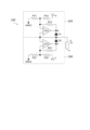
- FIG. 3 is an exemplary configuration diagram of a charging acceleration unit;
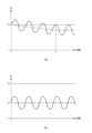
- FIG. 4 is an explanatory diagram of hysteresis characteristics; It is a figure which shows the conventional example of an impedance measuring apparatus.
- FIG. 1 is a configuration diagram showing a state in which a battery tester 200, which is an example of an impedance measuring device according to an embodiment of the present invention, is connected to a battery 230, which is an object to be measured.
- the battery tester 200 supplies a measuring alternating current Im from a measuring current source 210 to the battery 230, and measures the voltage Vm generated between the contact terminals Hp and Lp that contact both terminals of the battery 230 by the alternating current Im.
- This device measures the internal impedance Z of the battery 230 from the current Im supplied to the battery 230 and the measured voltage Vm measured by the unit 220 .
- Battery tester 200 connects coupling capacitor C3 from disconnection detection current supply unit 240 to current path 201 between measurement unit 220 and battery 230 in order to detect disconnection of current path 201 between measurement unit 220 and battery 230.
- the disconnection detection AC current Id is supplied through the wire breakage detection AC current Id, and the measurement unit 220 measures the voltage Vd generated between the contact terminals Hp and Lp that contact both terminals of the battery 230 by the disconnection detection AC current Id. , to detect a break in the current path 201 .
- the battery tester 200 has four contact terminals (high voltage side source terminal Hc, low voltage side source terminal Lc, high voltage side sense terminal Hp, low voltage side sense terminal Lp).
- a high voltage source terminal Hc and a high voltage sense terminal Hp are connected to the high voltage side of the battery 230 .
- the low voltage side source terminal Lc and the low voltage side sense terminal Lp are connected to the low voltage side of the battery 230 .
- the contact resistances between the high voltage source terminal Hc, the low voltage source terminal Lc, the high voltage side sense terminal Hp and the low voltage side sense terminal Lp, and the battery 230 are indicated by R Hc , R Lc , R Hp and R Lp , respectively.
- the high-voltage side source terminal Hc is connected to one end of the measuring current source 210 via the coupling capacitor C1.
- the other end of the measuring current source 210 and the low-voltage side source terminal Lc are connected to the ground GND1, which is the reference potential on the source side.
- the high voltage side sense terminal Hp is connected to the measuring section 220 via the coupling capacitor C2 and to the disconnection detecting current supply section 240 via the coupling capacitor C3.
- the low-voltage side sense terminal Lp is connected to the ground GND2, which is the reference potential on the sense side.
- the ground GND2 is also used as the reference potential for components arranged on the sense side, such as the measuring section 220 and the disconnection detection current supply section 240 .
- the ground GND1, which is the source-side reference potential, and the ground GND2, which is the sense-side reference potential, are electrically separated.
- a signal input to the measurement unit 220 via the coupling capacitor C2 is amplified by the non-inverting amplifier circuit of the operational amplifier OP1 and input to the calculation unit 221.
- An input of the measuring unit 220 is connected to the non-inverting input terminal of the operational amplifier OP1, one end of the resistor R1 and one end of the resistor R2 are connected to the inverting terminal, and the other end of the resistor R1 and the computing unit 221 are connected to the output terminal.
- the other end of resistor R2 is connected to ground GND2.
- the calculation unit 221 includes two lock-in amplifiers, and performs synchronous detection at the frequencies of the AC currents supplied from the measurement current source 210 and the disconnection detection current supply unit 240, respectively.
- the disconnection detection current supply unit 240 includes a disconnection detection current source 241, a charging acceleration unit 242, and a resistor R3, which are connected in parallel to the input.
- the disconnection detection current source 241 is a current source that supplies a disconnection detection AC current Id having a frequency different from the frequency of the measurement AC current Im.
- the disconnection detection AC current Id is supplied to the current path 201 between the measurement unit 220 and the battery 230 via the coupling capacitor C3.
- the voltage between both terminals of the disconnection detection current source 241 must be within the compliance voltage range.
- the absolute value of the voltage across the terminals of the battery 230 is generally larger than the absolute value of the compliance voltage. Therefore, prior to supplying the disconnection detection current Id, it is necessary to charge the coupling capacitor C3 so that the voltage between both terminals of the disconnection detection current source 241 is within the compliance voltage range.
- the resistor R3 has one end connected to the coupling capacitor C3 and the other end connected to the ground GND2. Therefore, the measurement current Im is divided between the battery 230 and the resistor R3. If the resistor R3 is small, the amount of current flowing into the resistor R3 increases, resulting in a measurement error. Therefore, it is desirable that the resistance R3 is large. Also, since it is desirable that the impedance of the coupling capacitor C3 is small, it is desirable that the capacitance be large. On the other hand, the charging time of the coupling capacitor C3 is proportional to the time constant of the resistor R3 and the coupling capacitor C3 if the charge acceleration unit 242 is not provided.
- the charge acceleration unit 242 monitors the voltage across both terminals of the disconnection detection current source 241, that is, the voltage Va at the point a. Accelerate the charging of the coupling capacitor C3 by supplying it to shorten the time until disconnection detection becomes possible.
- FIG. 2 shows an exemplary configuration of the charge acceleration unit 242.
- the charge acceleration unit 242 has a positive power supply hysteresis comparator 245 and a negative power supply hysteresis comparator 246 .
- the positive power supply hysteresis comparator 245 operates when the positive voltage battery 230 (the battery connected as shown in FIG. 1) is connected, and charges the coupling capacitor C3.
- the negative power supply hysteresis comparator 246 operates and charges the coupling capacitor C3 when the negative voltage battery 230 (the battery connected in reverse to FIG. 1) is connected.
- the positive power supply hysteresis comparator 245 includes an operational amplifier OP2, a diode D1 and three resistors R11, R12 and R13.
- the inverting terminal of the operational amplifier OP2 is connected to the output of the charging acceleration section 242 and the anode of the diode D1.
- a non-inverting terminal of the operational amplifier OP2 is connected to one ends of three resistors R11, R12, and R13.
- the output terminal of operational amplifier OP2 is connected to the cathode of diode D1 and the other end of resistor R13.
- the other end of the resistor R11 is connected to the ground GND2, and the other end of the resistor R12 is connected to the positive power source +V.
- the hysteresis characteristics (low-side threshold voltage and high-side threshold voltage) of the hysteresis comparator 245 are set by three resistors R11, R12, R13 and the magnitude of the positive power supply +V.
- the negative power supply hysteresis comparator 246 has a configuration symmetrical to the positive power supply hysteresis comparator 245 . That is, the negative power supply hysteresis comparator 246 includes an operational amplifier OP3, a diode D2, and three resistors R21, R22, and R23.
- the inverting terminal of the operational amplifier OP3 is connected to the output of the charge accelerating section 242 and the cathode of the diode D2.
- a non-inverting terminal of the operational amplifier OP3 is connected to one ends of three resistors R21, R22, and R23.
- the output terminal of operational amplifier OP3 is connected to the anode of diode D2 and the other end of resistor R23.
- the other end of the resistor R21 is connected to the ground GND2, and the other end of the resistor R22 is connected to the negative power supply -V.
- the hysteresis characteristics (low side threshold voltage and high side threshold voltage) of the hysteresis comparator 246 are set by three resistors R21, R22, R23 and the magnitude of the negative power supply -V.
- the positive power supply hysteresis comparator 245 and the negative power supply hysteresis comparator 246 charge the coupling capacitor C3 by similar operations, except for the polarity and the direction of the charging current. As an example, the operation of the charging acceleration unit 242 will be described.
- the voltage Va at the point a becomes substantially the same voltage as the voltage of the battery 230 because the coupling capacitor C3 is in an uncharged state. .
- the voltage between both terminals of the disconnection detection current source 241 greatly exceeds the compliance voltage of the disconnection detection current source 241, and the disconnection detection current source 241 cannot be operated normally.
- the voltage Va is also applied to the non-inverting terminal of the operational amplifier OP2 of the positive power supply hysteresis comparator 245, and compared with the voltage at the inverting terminal. potential equivalent to the supplied negative power supply voltage -V).
- charging current Ic flows from point a to point b through diode D1, and coupling capacitor C3 is charged.
- the voltage Va across the terminals of the current source 241 for disconnection detection decreases.
- the disconnection detection current source 241 When the charging of the coupling capacitor C3 progresses and the voltage Va becomes a predetermined voltage (low-side threshold voltage of the hysteresis comparator 245) smaller than the compliance voltage of the disconnection detection current source 241, the voltage at the output terminal (point b) of the operational amplifier OP2 Vb changes to a high voltage (equivalent to the positive power supply +V). Since the voltage on the cathode side of the diode D1 becomes high, the charging current Ic stops, and the operation of the charging acceleration section 242 stops. Since the voltage between both terminals of the disconnection detection current source 241 is equal to or less than the compliance voltage, the disconnection detection current source 241 can be normally operated to supply a normal disconnection detection current Id to perform disconnection detection.
- the voltage Va is obtained from the voltage of the battery 230, the voltage when the coupling capacitor C3 is fully charged, the path impedance of the current path 201, and the disconnection detection current Id. becomes a voltage on which the voltage drop of the product of is superimposed. Since the disconnection detection current Id is an alternating current, the voltage Va momentarily exceeds the voltage at the completion of charging of the coupling capacitor C3. At this time, if the charging acceleration unit 242 is restarted and the charging current Ic flows, part of the disconnection detection current Id will be diverted to the charging acceleration unit 242, making it impossible to accurately detect the disconnection.
- the hysteresis comparator 245 has a hysteresis characteristic, even if the voltage Va exceeds the low voltage side threshold voltage, it does not operate again until it exceeds the high voltage threshold voltage, and enters a high resistance state.
- the high voltage threshold voltage of the hysteresis comparator 245 By setting the high voltage threshold voltage of the hysteresis comparator 245 to be equal to or higher than the maximum voltage (instantaneous value) when the disconnection detection current Id is supplied, it is possible to prevent restarting when the disconnection detection current Id is supplied.
- the battery 230 is connected as shown in FIG. 1, and the coupling capacitor C3 is charged by the operation of the hysteresis comparator 245 of the positive power supply.
- the negative power supply hysteresis comparator 246 similarly operates to charge the coupling capacitor C3 (however, the polarity of the voltage and the direction of the charging current Ic are reversed).
- the charge acceleration part 242 determines that the voltage between both terminals of the disconnection detection current source is within a predetermined voltage range narrower than the compliance voltage of the disconnection detection current source. is exceeded, the coupling capacitor is charged and becomes a high resistance state in which current does not flow in or out except during charging.
- FIG. 3A and 3B are diagrams showing voltage waveforms at point a when the disconnection detection current Id is supplied, with the horizontal axis representing time and the vertical axis representing voltage.
- FIG. 3B shows a voltage waveform with no hysteresis characteristic.
- V1 is a voltage at which the charging acceleration section 242 stops supplying the charging current Ic, and is a low voltage side threshold voltage in the charging acceleration section 242 having hysteresis characteristics.
- V2 is the high side threshold voltage of the charge acceleration unit 242 having hysteresis characteristics.
- the charge acceleration unit 242 If the charge acceleration unit 242 does not have a hysteresis characteristic, the charge acceleration unit 242 restarts when Va exceeds V1 as the disconnection detection current Id is supplied. Therefore, the charging current Ic intermittently flows to charge the coupling capacitor C3, and the DC component of Va decreases as shown in FIG. 3(a). At time t1 , the maximum value (instantaneous value) of Va does not exceed V1 , and the operation of charging acceleration section 242 completely stops. Until time t1 , the voltage between both terminals of the disconnection detection current source 241 exceeds the compliance voltage, so normal operation of the disconnection detection current source 241 is not guaranteed, and disconnection detection cannot be performed.
- the charge acceleration unit 242 has a hysteresis characteristic, as shown in FIG . Unless otherwise, the charging acceleration unit 242 does not restart and maintains the high resistance state. Therefore, the disconnection detection current Id does not charge the coupling capacitor C3, and the disconnection can be detected immediately. Therefore, by having the hysteresis characteristic, disconnection can be detected in a shorter time than the time t1 .
- the charge acceleration unit 242 employs a hysteresis comparator for the positive power supply and the negative power supply.
- a programmable current source or the like may be used.
- Reference Signs List 100 impedance measuring devices 101 and 201 current paths 110 and 210 current sources for measurement 120 and 220 measuring section 130 objects to be measured 141 and 241 disconnection detection current source 200 impedance measuring device (battery tester) 230 DUT (battery) 240 disconnection detection current supply unit 242 charging acceleration unit 245 hysteresis comparator (positive power supply) 246 hysteresis comparator (negative supply) C1, C2, C3 Coupling capacitors D1, D2 Diodes GND1, GND2 Grounds Hc, Lc, Hp, Lp Contact terminals OP1, OP2, OP3 Operational amplifiers R1, R2, R3, R11, R12, R13, R21, R22, R23 Resistors R Hc , R Hp , R Lc , R Lp Contact resistance Z Internal impedance
Landscapes
- Physics & Mathematics (AREA)
- General Physics & Mathematics (AREA)
- Testing Of Short-Circuits, Discontinuities, Leakage, Or Incorrect Line Connections (AREA)
- Measurement Of Resistance Or Impedance (AREA)
Abstract
Description
101、201 電流路
110、210 測定用電流源
120、220 測定部
130 被測定物
141、241 断線検出用電流源
200 インピーダンス測定装置(バッテリテスタ)
230 被測定物(バッテリ)
240 断線検出用電流供給部
242 充電加速部
245 ヒステリシスコンパレータ(正電源)
246 ヒステリシスコンパレータ(負電源)
C1、C2、C3 カップリングコンデンサ
D1、D2 ダイオード
GND1、GND2 グランド
Hc、Lc、Hp、Lp 接触端子
OP1、OP2、OP3 オペアンプ
R1、R2、R3、R11、R12、R13、R21、R22、R23 抵抗
RHc、RHp、RLc、RLp 接触抵抗
Z 内部インピーダンス
Claims (4)
- 被測定物に供給された交流電流によって前記被測定物の両端子のそれぞれに接触する接触端子間に生ずる電圧を測定し、前記被測定物の内部インピーダンスを求める測定部と、
前記測定部と前記被測定物との電流路に、カップリングコンデンサを介して、断線検出用の交流電流を供給する断線検出用電流源と、
前記カップリングコンデンサと前記断線検出用電流源との間に接続され、前記断線検出用電流源の両端子間電圧が所定の電圧範囲を超えたときに、前記カップリングコンデンサを充電する充電加速部と、
を備える、インピーダンス測定装置。 - 前記所定の電圧範囲は、前記断線検出用電流源のコンプライアンス電圧より狭い、請求項1に記載のインピーダンス測定装置。
- 前記充電加速部は、ヒステリシス特性を有する、請求項1または2に記載のインピーダンス測定装置。
- 前記充電加速部は、正電源および負電源のヒステリシスコンパレータを備える、請求項3に記載のインピーダンス測定装置。
Priority Applications (3)
| Application Number | Priority Date | Filing Date | Title |
|---|---|---|---|
| EP22861129.9A EP4394401A4 (en) | 2021-08-26 | 2022-08-08 | IMPEDANCE MEASURING DEVICE |
| CN202280058045.7A CN117897624A (zh) | 2021-08-26 | 2022-08-08 | 阻抗测量装置 |
| US18/684,729 US20250334640A1 (en) | 2021-08-26 | 2022-08-08 | Impedance measuring device |
Applications Claiming Priority (2)
| Application Number | Priority Date | Filing Date | Title |
|---|---|---|---|
| JP2021-138307 | 2021-08-26 | ||
| JP2021138307A JP7569763B2 (ja) | 2021-08-26 | 2021-08-26 | インピーダンス測定装置 |
Publications (1)
| Publication Number | Publication Date |
|---|---|
| WO2023026839A1 true WO2023026839A1 (ja) | 2023-03-02 |
Family
ID=85323103
Family Applications (1)
| Application Number | Title | Priority Date | Filing Date |
|---|---|---|---|
| PCT/JP2022/030277 Ceased WO2023026839A1 (ja) | 2021-08-26 | 2022-08-08 | インピーダンス測定装置 |
Country Status (5)
| Country | Link |
|---|---|
| US (1) | US20250334640A1 (ja) |
| EP (1) | EP4394401A4 (ja) |
| JP (1) | JP7569763B2 (ja) |
| CN (1) | CN117897624A (ja) |
| WO (1) | WO2023026839A1 (ja) |
Cited By (1)
| Publication number | Priority date | Publication date | Assignee | Title |
|---|---|---|---|---|
| WO2025154664A1 (ja) * | 2024-01-15 | 2025-07-24 | 日置電機株式会社 | インピーダンス測定装置およびインピーダンス測定方法 |
Citations (6)
| Publication number | Priority date | Publication date | Assignee | Title |
|---|---|---|---|---|
| JPS6454423U (ja) * | 1987-09-29 | 1989-04-04 | ||
| JPH06130120A (ja) * | 1992-10-14 | 1994-05-13 | Matsushita Electron Corp | 半導体集積回路の試験方法 |
| JPH08153157A (ja) * | 1994-11-28 | 1996-06-11 | Nippondenso Co Ltd | 光学的情報読み取り装置 |
| US6255904B1 (en) * | 1998-12-16 | 2001-07-03 | Stmicroelectronics S.R.L. | Anti-pop circuit for AC amplifiers |
| JP4695920B2 (ja) | 2005-05-19 | 2011-06-08 | 日置電機株式会社 | インピーダンス測定装置 |
| JP2020076600A (ja) * | 2018-11-06 | 2020-05-21 | 日置電機株式会社 | インピーダンス測定装置 |
Family Cites Families (8)
| Publication number | Priority date | Publication date | Assignee | Title |
|---|---|---|---|---|
| JPH0442784Y2 (ja) * | 1984-12-24 | 1992-10-09 | ||
| JPH06104660A (ja) * | 1992-09-17 | 1994-04-15 | Fujitsu Ltd | 交流増幅回路 |
| JP3562623B2 (ja) * | 1998-10-07 | 2004-09-08 | 横河電機株式会社 | 計測装置 |
| JP4671768B2 (ja) * | 2005-06-07 | 2011-04-20 | 日置電機株式会社 | インピーダンス測定装置 |
| JP4735250B2 (ja) * | 2005-12-28 | 2011-07-27 | 横河電機株式会社 | 計測装置 |
| JP4913458B2 (ja) * | 2006-03-27 | 2012-04-11 | 日置電機株式会社 | 測定装置 |
| JP2009300343A (ja) * | 2008-06-17 | 2009-12-24 | Yokogawa Electric Corp | Icテスタ及びコンタクトチェック方法 |
| JP5619253B1 (ja) * | 2013-10-15 | 2014-11-05 | 三菱電機株式会社 | 誘導性負荷の給電制御装置 |
-
2021
- 2021-08-26 JP JP2021138307A patent/JP7569763B2/ja active Active
-
2022
- 2022-08-08 WO PCT/JP2022/030277 patent/WO2023026839A1/ja not_active Ceased
- 2022-08-08 CN CN202280058045.7A patent/CN117897624A/zh active Pending
- 2022-08-08 US US18/684,729 patent/US20250334640A1/en active Pending
- 2022-08-08 EP EP22861129.9A patent/EP4394401A4/en active Pending
Patent Citations (6)
| Publication number | Priority date | Publication date | Assignee | Title |
|---|---|---|---|---|
| JPS6454423U (ja) * | 1987-09-29 | 1989-04-04 | ||
| JPH06130120A (ja) * | 1992-10-14 | 1994-05-13 | Matsushita Electron Corp | 半導体集積回路の試験方法 |
| JPH08153157A (ja) * | 1994-11-28 | 1996-06-11 | Nippondenso Co Ltd | 光学的情報読み取り装置 |
| US6255904B1 (en) * | 1998-12-16 | 2001-07-03 | Stmicroelectronics S.R.L. | Anti-pop circuit for AC amplifiers |
| JP4695920B2 (ja) | 2005-05-19 | 2011-06-08 | 日置電機株式会社 | インピーダンス測定装置 |
| JP2020076600A (ja) * | 2018-11-06 | 2020-05-21 | 日置電機株式会社 | インピーダンス測定装置 |
Non-Patent Citations (1)
| Title |
|---|
| See also references of EP4394401A4 |
Cited By (1)
| Publication number | Priority date | Publication date | Assignee | Title |
|---|---|---|---|---|
| WO2025154664A1 (ja) * | 2024-01-15 | 2025-07-24 | 日置電機株式会社 | インピーダンス測定装置およびインピーダンス測定方法 |
Also Published As
| Publication number | Publication date |
|---|---|
| EP4394401A4 (en) | 2025-09-17 |
| US20250334640A1 (en) | 2025-10-30 |
| CN117897624A (zh) | 2024-04-16 |
| JP7569763B2 (ja) | 2024-10-18 |
| EP4394401A1 (en) | 2024-07-03 |
| JP2023032275A (ja) | 2023-03-09 |
Similar Documents
| Publication | Publication Date | Title |
|---|---|---|
| JP2004294437A (ja) | 電子バッテリテスタ | |
| WO2018192434A1 (zh) | 直流电源系统的绝缘电阻的检测电路及检测方法 | |
| JP3262819B2 (ja) | 接触判定回路を備えるインピーダンス測定装置及びその接触判定方法 | |
| CN101825651A (zh) | 探针卡、包括探针卡的半导体测试装置以及探针卡的熔丝检查方法 | |
| CN105319443B (zh) | 电容器的绝缘电阻测定装置 | |
| KR102365630B1 (ko) | 배터리 과전류 감지 장치 및 방법 | |
| JP7569763B2 (ja) | インピーダンス測定装置 | |
| US6674295B1 (en) | Impedance measuring apparatus for electronic component | |
| CN110676804B (zh) | 检测电路与使用其的开关模块 | |
| TW202238150A (zh) | 異物偵測方法及具有異物偵測功能之電源端 | |
| JP2015010880A (ja) | 絶縁検査装置 | |
| CN102937669B (zh) | 一种汽车电动滑门防夹条检测电路 | |
| JP6608234B2 (ja) | 接触判定装置および測定装置 | |
| CN113376441B (zh) | 一种薄膜电容器寄生电感参数的测量系统和方法 | |
| CN213122226U (zh) | 一种无线耳机充电盒的检测电路、充电盒和无线耳机 | |
| CN110221644B (zh) | 一种芯片及其外置rset电阻开路监测电路 | |
| US20050035767A1 (en) | Plug detector for an electrical test instrument | |
| JP2889264B2 (ja) | 四端子測定装置 | |
| CN107064719B (zh) | 一种开尔文连接故障检测电路及方法 | |
| US20140239970A1 (en) | Thermocouple open-circuit detection circuit and method | |
| US20250321151A1 (en) | System and method for detecting leaks with a leak detection cable | |
| JPH11281688A (ja) | 定電流源および抵抗測定装置 | |
| JPS5852543Y2 (ja) | 接触不良検出装置 | |
| JPH0524222Y2 (ja) | ||
| CN103869213A (zh) | 一种电源线电气通断测试装置 |
Legal Events
| Date | Code | Title | Description |
|---|---|---|---|
| 121 | Ep: the epo has been informed by wipo that ep was designated in this application |
Ref document number: 22861129 Country of ref document: EP Kind code of ref document: A1 |
|
| WWE | Wipo information: entry into national phase |
Ref document number: 202280058045.7 Country of ref document: CN |
|
| WWE | Wipo information: entry into national phase |
Ref document number: 2022861129 Country of ref document: EP |
|
| NENP | Non-entry into the national phase |
Ref country code: DE |
|
| ENP | Entry into the national phase |
Ref document number: 2022861129 Country of ref document: EP Effective date: 20240326 |
|
| WWP | Wipo information: published in national office |
Ref document number: 18684729 Country of ref document: US |