WO2023063228A1 - 負極材料、電池、負極材料の製造方法、及び電池の製造方法 - Google Patents
負極材料、電池、負極材料の製造方法、及び電池の製造方法 Download PDFInfo
- Publication number
- WO2023063228A1 WO2023063228A1 PCT/JP2022/037519 JP2022037519W WO2023063228A1 WO 2023063228 A1 WO2023063228 A1 WO 2023063228A1 JP 2022037519 W JP2022037519 W JP 2022037519W WO 2023063228 A1 WO2023063228 A1 WO 2023063228A1
- Authority
- WO
- WIPO (PCT)
- Prior art keywords
- silicon
- negative electrode
- electrode material
- less
- particles
- Prior art date
- Legal status (The legal status is an assumption and is not a legal conclusion. Google has not performed a legal analysis and makes no representation as to the accuracy of the status listed.)
- Ceased
Links
Images





Classifications
-
- C—CHEMISTRY; METALLURGY
- C01—INORGANIC CHEMISTRY
- C01B—NON-METALLIC ELEMENTS; COMPOUNDS THEREOF; METALLOIDS OR COMPOUNDS THEREOF NOT COVERED BY SUBCLASS C01C
- C01B33/00—Silicon; Compounds thereof
- C01B33/02—Silicon
-
- C—CHEMISTRY; METALLURGY
- C01—INORGANIC CHEMISTRY
- C01G—COMPOUNDS CONTAINING METALS NOT COVERED BY SUBCLASSES C01D OR C01F
- C01G41/00—Compounds of tungsten
- C01G41/006—Compounds containing tungsten, with or without oxygen or hydrogen, and containing two or more other elements
-
- H—ELECTRICITY
- H01—ELECTRIC ELEMENTS
- H01M—PROCESSES OR MEANS, e.g. BATTERIES, FOR THE DIRECT CONVERSION OF CHEMICAL ENERGY INTO ELECTRICAL ENERGY
- H01M10/00—Secondary cells; Manufacture thereof
- H01M10/05—Accumulators with non-aqueous electrolyte
- H01M10/052—Li-accumulators
- H01M10/0525—Rocking-chair batteries, i.e. batteries with lithium insertion or intercalation in both electrodes; Lithium-ion batteries
-
- H—ELECTRICITY
- H01—ELECTRIC ELEMENTS
- H01M—PROCESSES OR MEANS, e.g. BATTERIES, FOR THE DIRECT CONVERSION OF CHEMICAL ENERGY INTO ELECTRICAL ENERGY
- H01M4/00—Electrodes
- H01M4/02—Electrodes composed of, or comprising, active material
- H01M4/13—Electrodes for accumulators with non-aqueous electrolyte, e.g. for lithium-accumulators; Processes of manufacture thereof
- H01M4/134—Electrodes based on metals, Si or alloys
-
- H—ELECTRICITY
- H01—ELECTRIC ELEMENTS
- H01M—PROCESSES OR MEANS, e.g. BATTERIES, FOR THE DIRECT CONVERSION OF CHEMICAL ENERGY INTO ELECTRICAL ENERGY
- H01M4/00—Electrodes
- H01M4/02—Electrodes composed of, or comprising, active material
- H01M4/13—Electrodes for accumulators with non-aqueous electrolyte, e.g. for lithium-accumulators; Processes of manufacture thereof
- H01M4/139—Processes of manufacture
- H01M4/1395—Processes of manufacture of electrodes based on metals, Si or alloys
-
- H—ELECTRICITY
- H01—ELECTRIC ELEMENTS
- H01M—PROCESSES OR MEANS, e.g. BATTERIES, FOR THE DIRECT CONVERSION OF CHEMICAL ENERGY INTO ELECTRICAL ENERGY
- H01M4/00—Electrodes
- H01M4/02—Electrodes composed of, or comprising, active material
- H01M4/36—Selection of substances as active materials, active masses, active liquids
- H01M4/362—Composites
- H01M4/364—Composites as mixtures
-
- H—ELECTRICITY
- H01—ELECTRIC ELEMENTS
- H01M—PROCESSES OR MEANS, e.g. BATTERIES, FOR THE DIRECT CONVERSION OF CHEMICAL ENERGY INTO ELECTRICAL ENERGY
- H01M4/00—Electrodes
- H01M4/02—Electrodes composed of, or comprising, active material
- H01M4/36—Selection of substances as active materials, active masses, active liquids
- H01M4/362—Composites
- H01M4/366—Composites as layered products
-
- H—ELECTRICITY
- H01—ELECTRIC ELEMENTS
- H01M—PROCESSES OR MEANS, e.g. BATTERIES, FOR THE DIRECT CONVERSION OF CHEMICAL ENERGY INTO ELECTRICAL ENERGY
- H01M4/00—Electrodes
- H01M4/02—Electrodes composed of, or comprising, active material
- H01M4/36—Selection of substances as active materials, active masses, active liquids
- H01M4/38—Selection of substances as active materials, active masses, active liquids of elements or alloys
- H01M4/386—Silicon or alloys based on silicon
-
- H—ELECTRICITY
- H01—ELECTRIC ELEMENTS
- H01M—PROCESSES OR MEANS, e.g. BATTERIES, FOR THE DIRECT CONVERSION OF CHEMICAL ENERGY INTO ELECTRICAL ENERGY
- H01M4/00—Electrodes
- H01M4/02—Electrodes composed of, or comprising, active material
- H01M4/36—Selection of substances as active materials, active masses, active liquids
- H01M4/48—Selection of substances as active materials, active masses, active liquids of inorganic oxides or hydroxides
- H01M4/483—Selection of substances as active materials, active masses, active liquids of inorganic oxides or hydroxides for non-aqueous cells
-
- H—ELECTRICITY
- H01—ELECTRIC ELEMENTS
- H01M—PROCESSES OR MEANS, e.g. BATTERIES, FOR THE DIRECT CONVERSION OF CHEMICAL ENERGY INTO ELECTRICAL ENERGY
- H01M4/00—Electrodes
- H01M4/02—Electrodes composed of, or comprising, active material
- H01M4/36—Selection of substances as active materials, active masses, active liquids
- H01M4/58—Selection of substances as active materials, active masses, active liquids of inorganic compounds other than oxides or hydroxides, e.g. sulfides, selenides, tellurides, halogenides or LiCoFy; of polyanionic structures, e.g. phosphates, silicates or borates
- H01M4/583—Carbonaceous material, e.g. graphite-intercalation compounds or CFx
- H01M4/587—Carbonaceous material, e.g. graphite-intercalation compounds or CFx for inserting or intercalating light metals
-
- H—ELECTRICITY
- H01—ELECTRIC ELEMENTS
- H01M—PROCESSES OR MEANS, e.g. BATTERIES, FOR THE DIRECT CONVERSION OF CHEMICAL ENERGY INTO ELECTRICAL ENERGY
- H01M4/00—Electrodes
- H01M4/02—Electrodes composed of, or comprising, active material
- H01M4/62—Selection of inactive substances as ingredients for active masses, e.g. binders, fillers
-
- H—ELECTRICITY
- H01—ELECTRIC ELEMENTS
- H01M—PROCESSES OR MEANS, e.g. BATTERIES, FOR THE DIRECT CONVERSION OF CHEMICAL ENERGY INTO ELECTRICAL ENERGY
- H01M4/00—Electrodes
- H01M4/02—Electrodes composed of, or comprising, active material
- H01M4/62—Selection of inactive substances as ingredients for active masses, e.g. binders, fillers
- H01M4/624—Electric conductive fillers
- H01M4/625—Carbon or graphite
-
- C—CHEMISTRY; METALLURGY
- C01—INORGANIC CHEMISTRY
- C01P—INDEXING SCHEME RELATING TO STRUCTURAL AND PHYSICAL ASPECTS OF SOLID INORGANIC COMPOUNDS
- C01P2002/00—Crystal-structural characteristics
- C01P2002/80—Crystal-structural characteristics defined by measured data other than those specified in group C01P2002/70
- C01P2002/85—Crystal-structural characteristics defined by measured data other than those specified in group C01P2002/70 by XPS, EDX or EDAX data
-
- C—CHEMISTRY; METALLURGY
- C01—INORGANIC CHEMISTRY
- C01P—INDEXING SCHEME RELATING TO STRUCTURAL AND PHYSICAL ASPECTS OF SOLID INORGANIC COMPOUNDS
- C01P2004/00—Particle morphology
- C01P2004/51—Particles with a specific particle size distribution
-
- C—CHEMISTRY; METALLURGY
- C01—INORGANIC CHEMISTRY
- C01P—INDEXING SCHEME RELATING TO STRUCTURAL AND PHYSICAL ASPECTS OF SOLID INORGANIC COMPOUNDS
- C01P2006/00—Physical properties of inorganic compounds
- C01P2006/40—Electric properties
-
- H—ELECTRICITY
- H01—ELECTRIC ELEMENTS
- H01M—PROCESSES OR MEANS, e.g. BATTERIES, FOR THE DIRECT CONVERSION OF CHEMICAL ENERGY INTO ELECTRICAL ENERGY
- H01M4/00—Electrodes
- H01M4/02—Electrodes composed of, or comprising, active material
- H01M2004/026—Electrodes composed of, or comprising, active material characterised by the polarity
- H01M2004/027—Negative electrodes
-
- Y—GENERAL TAGGING OF NEW TECHNOLOGICAL DEVELOPMENTS; GENERAL TAGGING OF CROSS-SECTIONAL TECHNOLOGIES SPANNING OVER SEVERAL SECTIONS OF THE IPC; TECHNICAL SUBJECTS COVERED BY FORMER USPC CROSS-REFERENCE ART COLLECTIONS [XRACs] AND DIGESTS
- Y02—TECHNOLOGIES OR APPLICATIONS FOR MITIGATION OR ADAPTATION AGAINST CLIMATE CHANGE
- Y02E—REDUCTION OF GREENHOUSE GAS [GHG] EMISSIONS, RELATED TO ENERGY GENERATION, TRANSMISSION OR DISTRIBUTION
- Y02E60/00—Enabling technologies; Technologies with a potential or indirect contribution to GHG emissions mitigation
- Y02E60/10—Energy storage using batteries
Definitions
- the present invention relates to a negative electrode material, a battery, a method for manufacturing a negative electrode material, and a method for manufacturing a battery.
- Patent Document 1 describes a negative electrode in which tungsten trioxide is arranged on the surface of graphite. By arranging tungsten trioxide on the surface of graphite, it becomes possible to improve the diffusibility of lithium ions, and the performance of the battery can be improved. Further, for example, Patent Document 2 describes a negative electrode containing silicon grains (silicon), tungsten, and carbon.
- the performance can be improved by providing a tungsten compound such as tungsten trioxide or silicon, but there is room for improvement in improving the performance.
- the present invention has been made in view of the above, and an object of the present invention is to provide a negative electrode material and a battery with improved performance, a method for manufacturing the negative electrode material, and a method for manufacturing the battery.
- the present disclosure provides a negative electrode material for a battery, the negative electrode material comprising carbon, sodium tungstate, and a silicon material containing silicon, wherein the silicon In the material, the ratio of the Si amount of Si2p derived from simple silicon to the amount of Si2p derived from SiO2 in the surface layer is 3 or more on the basis of atomic concentration, when measured by X-ray photoelectron spectroscopy.
- the battery according to the present disclosure includes the negative electrode material and the positive electrode material.
- the method for producing a negative electrode material is a method for producing a negative electrode material for a battery, in which a silicon raw material is prepared in an atmosphere with an oxygen concentration of 5% or less. and using the silicon source material to produce a negative electrode material comprising carbon, sodium tungstate, and a silicon material, wherein the silicon material has a surface layer thickness as measured by X-ray photoelectron spectroscopy.
- the ratio of the amount of Si in Si 2p derived from elemental silicon to the amount of Si in Si 2p derived from SiO 2 in is 3 or more on an atomic concentration basis.
- the method of manufacturing a battery according to the present disclosure includes the method of manufacturing the negative electrode material and the step of manufacturing the positive electrode material.
- the performance of the negative electrode material can be improved.
- FIG. 1 is a schematic partial cross-sectional view of a battery according to this embodiment.
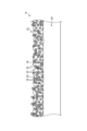
- FIG. 2 is a schematic cross-sectional view of an example of the negative electrode according to this embodiment.
- FIG. 3 is a schematic cross-sectional view of a silicon material.
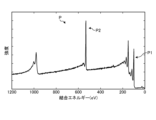
- FIG. 4 is a diagram showing an example of a survey spectrum showing the results of XPS measurement of a silicon material.
- FIG. 5 is a diagram showing an example of a Si2p narrow spectrum showing the result of XPS measurement of a silicon material.
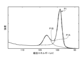
- FIG. 6 is a diagram showing an example of peak separation of a Si2p narrow spectrum showing the result of XPS measurement of a silicon material.
- FIG. 1 is a schematic partial cross-sectional view of a battery according to this embodiment.
- FIG. 2 is a schematic cross-sectional view of an example of the negative electrode according to this embodiment.
- FIG. 3 is a schematic cross-sectional view of a silicon material.
- FIG. 4 is a diagram showing an example of
- FIG. 7 is a diagram showing an example of a narrow spectrum of O1s showing the result of XPS measurement of a silicon material.
- FIG. 8 is a flow chart illustrating the steps of preparing a silicon source.
- FIG. 9 is a flow chart illustrating an example of a method for manufacturing a battery according to this embodiment.
- FIG. 10 is a table showing the manufacturing conditions of each example and the characteristics of the silicon material.
- FIG. 11 is a table showing the identification results of the negative electrode material and the battery characteristic results of each example.
- FIG. 1 is a schematic partial cross-sectional view of a battery according to this embodiment.
- a battery 1 according to this embodiment is a lithium ion secondary battery.
- the battery 1 includes a casing 10, an electrode group 12, and an electrolyte (not shown).
- the casing 10 is a case that accommodates the electrode group 12 and the electrolytic solution inside.
- the casing 10 may also include wiring, terminals, and the like connected to the electrode group 12 .
- the electrode group 12 includes a negative electrode 14, a positive electrode 16, and a separator 18.
- the electrode group 12 has a configuration in which a separator 18 is arranged between a negative electrode 14 and a positive electrode 16 .
- the electrode group 12 has a so-called laminated electrode group structure in which rectangular negative electrodes 14 and rectangular positive electrodes 16 are alternately laminated with rectangular separators 18 interposed therebetween.
- the electrode group 12 is not limited to the stacked electrode group structure.
- the electrode group 12 may have a wound electrode group structure in which a strip-shaped negative electrode 14 and a strip-shaped positive electrode 16 are laminated with a strip-shaped separator 18 interposed therebetween, and these are wound. good.
- FIG. 2 is a schematic cross-sectional view of an example of the negative electrode according to this embodiment.
- the negative electrode 14 includes a current collecting layer 20 and a negative electrode material layer 22 .
- the current collecting layer 20 is a layer made of a conductive member. Examples of the conductive member of the current collecting layer 20 include copper.
- the negative electrode material layer 22 is a layer containing the negative electrode material according to this embodiment.
- the negative electrode material layer 22 is provided on the surface of the current collecting layer 20 .
- the thickness of the current collecting layer 20 may be, for example, about 15 ⁇ m to 40 ⁇ m, and the thickness of the negative electrode material layer 22 may be, for example, about 20 ⁇ m to 200 ⁇ m.
- the negative electrode 14 may include negative electrode material layers 22 on both sides of the current collecting layer 20 .
- the negative electrode material layer 22 contains a negative electrode material.
- the negative electrode material includes carbon, sodium tungstate, and silicon material (silicon particles).
- Sodium tungstate is a tungsten compound represented by Na x WO y , where x and y are numbers greater than zero. Details of Na x WO y will be described later.
- sodium tungstate is provided on the surface of carbon, and a silicon material is provided on the surface of carbon. good.
- the negative electrode material of the negative electrode material layer 22 includes carbon particles 30 that are carbon particles, Na x WO y (sodium tungstate) particles 32 that are sodium tungstate particles, and particles containing silicon. some silicon particles 33;
- the shape of the particles here is not limited to a spherical shape, and may be of any shape such as a linear shape or a sheet shape. Furthermore, the particle surface may be smooth or uneven.
- Sodium tungstate provided on the surface of carbon means that sodium tungstate directly adheres to carbon, that sodium tungstate indirectly adheres to carbon through silicon adhered to carbon, and that sodium tungstate is adhered to carbon indirectly. and that the composite particles in which sodium tungstate and silicon are directly fixed to the carbon are directly or indirectly fixed to the carbon.
- the negative electrode material in this embodiment preferably contains at least carbon and a silicon material to which sodium tungstate is adhered.
- the negative electrode material of the present embodiment is composed of carbon, sodium tungstate, and a silicon material, and may contain only carbon, sodium tungstate, and a silicon material, except for unavoidable impurities.
- the negative electrode material of this embodiment may contain unavoidable impurities in the balance.
- the negative electrode material of the negative electrode material layer 22 contains a plurality of carbon particles 30 .
- the carbon particles 30 contain amorphous carbon or graphite.
- Amorphous carbon is amorphous carbon that does not have a crystal structure.
- Amorphous carbon is sometimes called amorphous carbon or diamond-like carbon, and can be said to be carbon in which sp2 bonds and sp3 bonds are mixed.
- Carbon particles of amorphous carbon preferably consist entirely of amorphous carbon and do not contain components other than amorphous carbon, except for inevitable impurities. Specifically, carbon particles of amorphous carbon preferably do not contain graphite.
- Amorphous carbon may also contain functional groups (eg, hydroxy groups, carboxyl groups) on the surface during treatment to place sodium tungstate on the surface.
- this functional group allows sodium tungstate to be properly trapped on the surface of the amorphous carbon, and sodium tungstate can be appropriately arranged on the surface.
- the sodium tungstate is fixed to the surface of the amorphous carbon by this functional group, the adhesion of the sodium tungstate to the surface of the amorphous carbon can be increased, and the sodium tungstate is separated from the surface of the carbon. can be suppressed.
- the functional groups tend to remain without being removed, and sodium tungstate and silicon can be appropriately arranged on the surface.
- Graphite is carbon with a planar crystal structure.
- the average particle diameter of the carbon particles 30 is preferably 1 ⁇ m or more and 50 ⁇ m or less, more preferably 1 ⁇ m or more and 20 ⁇ m or less. When the average particle diameter is within this range, the strength of the electrode film can be maintained.
- the negative electrode material of the negative electrode material layer 22 further includes a plurality of Na x WO y particles 32 and silicon particles (silicon material) 33 . More specifically, a plurality of Na x WO y particles 32 and silicon particles 33 are provided for each carbon particle 30 .
- One Na x WO y particle 32 of the plurality of Na x WO y particles 32 is provided on the surface of the carbon particle 30 .
- the other Na x WO y particles 32 of the plurality of Na x WO y particles 32 are provided on the surfaces of the silicon particles 33 .
- the silicon particles 33 are in close contact with (contact with) the surfaces of the carbon particles 30
- the Na x WO y particles 32 are in close contact with (contact with) the surfaces of the silicon particles 33 .
- Carbon particles 30, Na x WO y particles 32 and silicon particles 33 may be combined.
- carbon particles 30 and silicon particles 33 may be combined, and carbon particles 30 and Na x WO y particles 32 may be combined. Therefore, the negative electrode material of the negative electrode material layer 22 has a structure in which the carbon particles 30, the Na x WO y particles 32, and the silicon particles 33 are combined, and the carbon particles 30 and the silicon particles 33 are further combined.
- At least one of a structure and a structure in which the carbon particles 30 and the Na x WO y particles 32 are combined may be included.
- sodium tungstate may take not only the form of Na x WO y but also the form of Na 2 WO 4 and Na 5 W 14 O 44 in terms of crystal structure.
- Na 2 WO 4 can be represented by the chemical formula Na x WO y because Na has a valence of 2, W has a valence of 1, and O has a valence of 4.
- Na 5 W 14 O 44 is represented by the chemical formula of Na 5/14 WO 44/14 (that is, the valence of Na is 5/14, the valence of W is is 1, and the valence of O is 44/14), it can be said to be represented by the chemical formula Na x WO y . That is, sodium tungstate represented by the chemical formula Na x WO y refers to sodium tungstate in which the ratio of the valence of Na, the valence of W, and the valence of O is X:1:Y. I can say
- Compositing here means separating the silicon particles 33 from the carbon particles 30, separating the silicon particles 33 from the Na x WO y particles 32, and separating the Na x WO y particles 32, at least when no external force acts. It refers to a state in which it is impossible to separate from the carbon particles 30 .
- the external force refers to the force when an SEI (Solid Electrolyte Interphase) film is formed covering the entire surface layer and expands and contracts when a battery using the negative electrode material is operated.
- compositing means forming a composite in which silicon particles 33 are arranged on the surfaces of carbon particles 30 and Na x WO y particles 32 are arranged on the surfaces of the silicon particles 33 , and Na x WO y particles 32 are arranged on the surfaces of the carbon particles 30 .
- the Na x WO y particles 32 contained in the negative electrode material of the negative electrode material layer 22 preferably have y (the valence of O) of 3, in other words, preferably Na x WO 3 .
- the Na x WO y particles 32 contained in the negative electrode material of the negative electrode material layer 22 have x (valence of Na) greater than 0 and 1 or less and y (valence of O) of 2 or more and 4 or less.
- the Na x WO y particles 32 preferably have a valence of x of 0.1 or more and 0.95 or less and a y of 2.5 or more and 3.5 or less.
- the Na x WO y particles 32 can be appropriately arranged on the surface of the carbon particles 30 .
- the negative electrode material of the negative electrode material layer 22 may contain only one type of Na x WO y particles 32 or may contain multiple types of Na x WO y particles 32 . Further, the negative electrode material of the negative electrode material layer 22 includes Na 0.78 WO 3 , Na 0.48 WO 3 , Na 0.72 WO 3 , Na 0.44 WO 3 , Na 0.44 WO 3 as the Na x WO y particles 32 .
- the negative electrode material of the negative electrode material layer 22 in the present embodiment includes Na 0.78 WO 3 , Na 0.48 WO 3 , Na 0.72 WO 3 , Na 0.44 WO 3 , Na 0.44 WO 3 as sodium tungstate. It preferably contains at least one of Na0.49WO3 , Na0.33WO3 , Na0.58WO3 , Na2WO4 , and Na5W14O44 .
- XRD X-Ray Diffraction
- XRD measurement conditions may be, for example, as follows.
- ICDD PDF2.DAT
- PDF2.DAT International Center for Diffraction Data
- PDXL2 which is integrated powder X-ray diffraction software
- XRD crystalline peaks detected by XRD
- PDXL2 which is integrated powder X-ray diffraction software
- the same software is used to extract compounds whose FOM (figure of merit) is equal to or less than the threshold, and compounds whose FOM is equal to or less than the threshold are identified as compounds contained in the measurement sample (negative electrode material in this case).
- the FOM threshold may be 10.
- the FOM of the diffraction peak of the negative electrode material with respect to the diffraction peak of Na 0.3 WO 3 in ICDD is a threshold value (for example, 10) or less, it is determined that the negative electrode material contains Na 0.3 WO 3 .
- a threshold value for example, 10
- the peak waveform in the X-ray diffraction analysis result of the analyte shows the peak waveform of carbon, but the (002) peak waveform in the known graphite structure becomes broad, it can be determined to be amorphous carbon.
- the Na x WO y particles 32 preferably include at least one of a cubic crystal structure, a tetragonal crystal structure, and a triclinic crystal structure. That is, the negative electrode material may have only cubic crystals as the Na x WO y particles 32, may have only tetragonal crystals, or may have only triclinic crystals. may have both a cubic crystal and a tetragonal crystal, may have both a cubic crystal and a triclinic crystal, or may have both a tetragonal crystal and a triclinic crystal It may have a cubic crystal, a tetragonal crystal, and a triclinic crystal.
- the negative electrode material of the negative electrode material layer 22 contains both cubic and tetragonal Na x WO y particles 32
- the tetragonal Na x WO y particles are preferred over the cubic Na x WO y particles 32 .
- Many particles 32 may be included.
- the content of the triclinic crystal may be less than that of the other crystal structures.
- cubic Na x WO y include Na 0.3 WO 3 , Na 0.78 WO 3 , Na 0.72 WO 3 , Na 0.44 WO 3 , Na 0.49 WO 3 and Na 0.49 WO 3 .
- Examples of tetragonal NaxWOy include Na0.1WO3 , Na0.48WO3 and Na0.33WO3 .
- Examples of orthorhombic Na x WO y include Na 5 W 14 O 44 .
- the crystal structure of tungsten trioxide contained in the negative electrode material is not limited to this, and for example, tungsten trioxide with other crystal structures may be included.
- the negative electrode material may also contain amorphous tungsten trioxide. It should be noted that the crystal structure of the Na x WO y particles 32 can also be identified by a method similar to the identification of the compound contained in the negative electrode material.
- the average particle size of the Na x WO y particles 32 is preferably smaller than the average particle size of the carbon particles 30 .
- the average particle size of the Na x WO y particles 32 is preferably 100 nm or more and 20 ⁇ m or less, more preferably 100 nm or more and 1 ⁇ m or less.
- the negative electrode material has a structure in which particulate sodium tungstate (Na x WO y particles 32) and silicon material (silicon particles 33) are provided on the surface of the carbon particles 30; can't
- the negative electrode material may have a structure in which sodium tungstate and silicon material are provided on the surface of carbon, and the shape of the sodium tungstate and silicon material provided on the surface of carbon may be arbitrary.
- silicon fine particles are used as the silicon particles 33 in this embodiment, silicon compound fine particles may be used.
- the content of sodium tungstate (Na x WO y particles 32) in the negative electrode material can be confirmed by measuring the content of Na, W, and O by fluorescent X-ray analysis. That is, at least part of the total amount of Na, W, and O detected by the fluorescent X-ray analysis constitutes sodium tungstate (Na x WO y particles 32), so depending on the content of Na, W, and O The content of sodium tungstate can be confirmed.
- the negative electrode material has a Na content of 0.01% or more and 0.5% or less by mass and a W content of 0.5% or more by mass when measured by fluorescent X-ray analysis. It is 20% or less, and the content of O is preferably 1% or more and 15% or less in mass ratio.
- the negative electrode material has a Na content of 0.02% or more and 0.4% or less by mass, and a W content of 0.7 by mass, when measured by fluorescent X-ray analysis. % or more and 17% or less, and the content of O is more preferably 2% or more and 13% or less in mass ratio.
- the negative electrode material has a Na content of 0.03% or more and 0.3% or less in mass ratio, and a W content of 1% or more in mass ratio, when measured by fluorescent X-ray analysis. It is 15% or less, and the content of O is more preferably 3% or more and 12% or less in mass ratio.
- the content of C measured by fluorescent X-ray analysis is preferably 60% or more and 95% or less, more preferably 65% or more and 95% or less, in terms of mass ratio. % or more and 92% or less.
- the tungsten compound can be appropriately arranged on the surface of the carbon.
- Na/W which is the ratio of the content of Na to the content of W, when measured by fluorescent X-ray analysis
- W/C which is the ratio of the W content to the C content, measured by fluorescent X-ray analysis
- W/C is 0.005 or more and 0.3 or less in terms of mass ratio. It is preferably 0.008 or more and 0.25 or less, and still more preferably 0.01 or more and 0.2 or less.
- the content of silicon particles 33 in the negative electrode material can be confirmed by measuring the content of Si by fluorescent X-ray analysis. That is, at least part of the total amount of Si detected by fluorescent X-ray analysis constitutes silicon particles 33 .
- the negative electrode material preferably has a Si content of 1% or more and 15% or less, more preferably 2% or more and 12% or less, as measured by X-ray fluorescence analysis. % or more and 10% or less. By setting the Si content within this range, the silicon particles 33 can be appropriately arranged on the surface of the carbon.
- the negative electrode material preferably has a mass ratio of Si/C, which is the ratio of the Si content to the C content, of 0.01 or more and 0.3 or less when measured by fluorescent X-ray analysis. It is more preferably 0.02 or more and 0.25 or less, and still more preferably 0.03 or more and 0.15 or less.
- Si/W which is the ratio of the Si content to the W content, when measured by fluorescent X-ray analysis, is preferably 0.1 or more and 15 or less in terms of mass ratio. It is more preferably 0.15 or more and 12 or less, and still more preferably 0.2 or more and 10 or less.
- Si/O which is the ratio of the Si content to the O content when measured by fluorescent X-ray analysis, is preferably 0.1 or more and 2 or less in terms of mass ratio. It is more preferably 0.2 or more and 1.5 or less, and still more preferably 0.3 or more and 1.3 or less. By setting the content ratio within these ranges, the tungsten compound can be appropriately arranged on the surface of the carbon.
- the fluorescent X-ray analysis may be performed using a wavelength dispersive X-ray fluorescent spectrometer, and the measurement conditions may be as follows.
- ⁇ Measuring device ZSX PrimusIV manufactured by Rigaku Corporation
- ⁇ Tube voltage 30 kV
- ⁇ Tube current 100mA
- the standardless fundamental parameter method may be used as the measurement method, and the SQX scattered radiation FP method of Rigaku may be used for the analysis.
- the negative electrode material layer 22 may contain substances other than the negative electrode material (carbon particles 30, Na x WO y particles 32 and silicon particles 33).
- the negative electrode material layer 22 may contain, for example, a binder. Any material may be used for the binder, and examples thereof include polyvinylidene fluoride (PVDF), carboxymethyl cellulose (CMC), styrene-butadiene rubber (SBR), and polyacrylic acid (PAA). Only one type of binder may be used, or two or more types may be used in combination. However, when the carbon particles 30 are amorphous carbon, the negative electrode material layer 22, in other words, the negative electrode material, preferably does not contain graphite.
- PVDF polyvinylidene fluoride
- CMC carboxymethyl cellulose
- SBR styrene-butadiene rubber
- PAA polyacrylic acid
- the fact that the Na x WO y particles 32 and the silicon particles 33 are arranged on the surface of the carbon particles 30 can be confirmed by observing with an electron microscope such as a SEM (Scanning Electron Microscope) or a TEM (Transmission Electron Microscope). can be confirmed.
- an electron microscope such as a SEM (Scanning Electron Microscope) or a TEM (Transmission Electron Microscope).
- the negative electrode material has a structure in which particulate sodium tungstate (Na x WO y particles 32 ) and silicon particles 33 are provided on the surface of the carbon particles 30 , but the structure is not limited thereto.
- the negative electrode material may have a structure in which sodium tungstate and silicon material are provided on the surface of carbon, and the shape of the sodium tungstate and silicon material provided on the surface of carbon may be arbitrary.
- FIG. 3 is a schematic cross-sectional view of the silicon material before being added.
- silicon particle 33 includes Si layer 33A and oxide layer 33B.
- the Si layer 33A is a layer made of Si, and can be said to be a core portion of the silicon particles 33 .
- the Si layer 33A preferably does not contain elements other than Si, except for inevitable impurities.
- the oxide layer 33B is a layer formed on the surface of the Si layer 33A, and preferably covers the entire surface of the Si layer 33A.
- the oxide layer 33B can be said to be the outermost surface layer of the silicon particles 33 .
- the oxide layer 33B is a layer made of silicon oxide (SiO x ).
- the oxide layer 33B contains SiO 2 as a silicon oxide, but may contain silicon oxides other than SiO 2 , for example, SiO. It is preferable that the oxide layer 33B does not contain elements other than the elements constituting the oxide of silicon, except for unavoidable impurities.
- ⁇ Measuring device PHI5000 Versa Probe II (manufactured by ULVAC-PHI) ⁇ Excitation X-ray: Monochrome AlK ⁇ ray ⁇ Output: 50W ⁇ Pass energy: 187.85 eV (Survey), 46.95 eV (Narrow) ⁇ Measurement interval: 0.8 eV/step (Survey), 0.1 eV/step (Narrow) ⁇ Photoelectron extraction angle with respect to the sample surface: 45° ⁇ X-ray diameter: 200 ⁇ m
- the ratio of the amount of Si in Si2p derived from simple silicon to the amount of Si in Si2p derived from SiO2 in the surface layer when measured by X-ray photoelectron spectroscopy is 3.0 on an atomic concentration basis. , preferably 3.5 or more, more preferably 4 or more.
- surface layer refers to the range from the surface to the depth at which photoelectrons can escape from the sample.
- Si in Si2p refers to Si atoms from which 2p orbital electrons have been ejected by X-ray photoelectron spectroscopy.
- Si of Si2p derived from SiO2 refers to Si constituting SiO2 from which electrons in the 2p orbital have jumped out by X-ray photoelectron spectroscopy, and Si of Si2p derived from elemental silicon means 2p Si by X-ray photoelectron spectroscopy. It refers to Si that constitutes elemental silicon (metallic silicon) from which electrons in the orbit are ejected.
- the ratio of the amount of Si in Si2p derived from simple silicon to the amount of Si in Si2p derived from SiO2 in the surface layer is the surface layer (here, for example, from the outermost surface of the silicon particle 33 to a position approximately 6 angstroms deeper than the outermost surface. ), refers to the ratio of the atomic concentration of Si (Si atoms) derived from simple silicon from which 2p orbital electrons have popped to the atomic concentration of Si (Si atoms) derived from SiO 2 from which 2p orbital electrons have popped.
- the ratio of the amount of Si in Si2p derived from simple silicon to Si in Si2p derived from SiO2 is within this range (3.0 or more), so that the amount of oxide near the surface is reduced, The capacity of the negative electrode material can be improved.
- the oxide layer on the surface becomes thin, the intrusion and desorption of Li ions become easier, and the impedance decreases.
- the ratio of the amount of Si of Si2p derived from simple silicon to the amount of Si of Si2p derived from SiO2 in the surface layer when measured by X-ray photoelectron spectroscopy is 9 or less on the basis of atomic concentration. is preferred, 19 or less is more preferred, and 99 or less is even more preferred.
- the ratio of the amount of Si to the amount of SiO 2 is in this range (99 or less), so there is no need to prepare equipment or processes for preventing excessive oxidation of the silicon material, and the negative electrode material It is possible to suppress the decrease in productivity while improving the capacity of
- the ratio of the amount of Si in Si2p derived from simple silicon to the amount of Si in Si2p derived from SiO2 in the surface layer is the atomic concentration standard , preferably 3 or more and 9 or less, more preferably 3 or more and 19 or less, and even more preferably 3 or more and 99 or less.
- the ratio of the amount of Si in Si2p derived from simple silicon to the amount of Si in Si2p derived from SiO2 in the surface layer is, on an atomic concentration basis, It is preferably 3.5 or more and 9 or less, more preferably 3.5 or more and 19 or less, and even more preferably 3.5 or more and 99 or less.
- the ratio of the amount of Si in Si2p derived from simple silicon to the amount of Si in Si2p derived from SiO2 in the surface layer is, on an atomic concentration basis, It is preferably 4 or more and 9 or less, more preferably 4 or more and 19 or less, and even more preferably 4 or more and 99 or less.
- the amount of Si in Si2p derived from SiO2 is 1%
- the amount of Si in Si2p derived from simple silicon is 99%.
- the ratio of the amount of Si to Si2p derived from elemental silicon is 99.
- the amount of Si in Si2p derived from SiO2 is 5%
- the amount of Si in Si2p derived from simple silicon is 95%.
- the ratio of the amount of Si to Si2p derived from elemental silicon is 19.
- FIG. 4 is a diagram showing an example of a survey spectrum showing the XPS measurement results of a silicon material
- FIG. 5 is a diagram showing an example of a Si2p narrow spectrum showing the XPS measurement results of a silicon material
- FIG. 7 is a diagram showing an example of peak separation of the Si2p narrow spectrum showing the XPS measurement results of the silicon material
- FIG. 7 is a diagram showing an example of the O1s narrow spectrum showing the XPS measurement results of the silicon material. .
- FIG. 4 shows an example of the peak waveform P of the silicon particles 33 in wide scan analysis, and the peak waveform P1 near the binding energy of 100 eV indicates the peak of Si2p.
- FIG. 5 is an example of the narrow spectrum of the silicon particles 33 in the narrow scan analysis near the peak waveform P1, in which the background is removed and the Si2p peak is extracted.
- Si of Si2p derived from SiO2 and Si of Si2p derived from elemental silicon differ in bond energy due to the difference in bond state. Therefore, as shown in FIG. 6, the peak waveform P1 can be separated into a peak waveform P1A indicating Si2p derived from elemental silicon and a peak waveform P1B indicating Si2p derived from SiO2 .
- the peak waveform P1A is a waveform having one peak near binding energy 99 eV
- the peak waveform P1B is a waveform having one peak near binding energy 103 eV.
- Multipak version 9.9.0.8 attached to the X-ray photoelectron spectrometer was used as software to remove the background from the peak waveform, and the baseline was corrected mainly by the Shirley method.
- the ratio of the area of the peak waveform P1A to the area of the peak waveform P1B is calculated as the ratio of the amount of Si in Si2p derived from simple silicon to the amount of Si in Si2p derived from SiO 2 on the atomic concentration basis. .
- Si-derived Si concentration ratio the ratio of the atomic concentration of Si of Si2p derived from simple silicon to the atomic concentration of Si of all Si2p (all Si from which 2p orbital electrons have escaped) in the surface layer of the silicon particle 33 is defined as the Si concentration of Si derived from Si.
- the Si concentration ratio derived from Si can be calculated as the ratio of the area of the peak waveform P1A to the area of the peak waveform P1.
- the Si concentration ratio derived from Si is preferably 75% or more, more preferably 77% or more, and even more preferably 80% or more.
- the concentration ratio of Si derived from Si falls within this range, the amount of oxide in the vicinity of the surface is reduced, and the capacity of the negative electrode material can be improved.
- the Si concentration ratio derived from Si is preferably 90% or less, more preferably 95% or less, and even more preferably 99% or less. When the Si concentration ratio derived from Si is within this range, there is no need to prepare equipment and processes to prevent excessive oxidation of the silicon material, and the capacity of the negative electrode material is improved, while suppressing a decrease in productivity. can.
- Si concentration ratio derived from SiO2 the ratio of the Si atomic concentration of Si 2p derived from SiO 2 to the atomic concentration of Si of all Si 2p in the surface layer of the silicon particles 33 is defined as the Si concentration ratio derived from SiO 2 .
- the Si concentration ratio derived from SiO 2 can be calculated as the ratio of the area of the peak waveform P1B to the area of the peak waveform P1.
- the Si concentration ratio derived from SiO 2 is preferably 25% or less, more preferably 24% or less, and even more preferably 20% or less. When the concentration ratio of Si derived from SiO 2 falls within this range, the amount of oxides in the vicinity of the surface is reduced, and the capacity of the negative electrode material can be improved.
- the Si concentration ratio derived from SiO 2 is preferably 10% or more, more preferably 5% or more, and even more preferably 1% or more.
- the Si concentration ratio derived from SiO2 is within this range, there is no need to prepare equipment and processes for preventing excessive oxidation of the silicon material, and the capacity of the negative electrode material is improved, while reducing productivity. can be suppressed.
- the ratio of the amount of Si in Si2p to the amount of O in O1s in the surface layer, when measured by X-ray photoelectron spectroscopy, is preferably 1.0 or more on the atomic concentration basis. It is more preferably 1 or more, and even more preferably 1.3 or more.
- the O in O1s refers to an O atom from which an electron in the 1s orbit is ejected by X-ray photoelectron spectroscopy.
- the ratio of the amount of Si in Si2p to the amount of O in O1s in the surface layer is the O of O1s (1s orbital Atomic concentration of Si of Si2p (Si atoms from which electrons in the 2p orbital have escaped) in the surface layer of the silicon particle 33 (for example, to a position approximately 6 angstroms deeper than the outermost surface) relative to the atomic concentration of O atoms from which electrons have escaped. refers to the ratio of In the silicon particles 33, when the ratio of the amount of Si in Si2p to the amount of O in O1s is within this range, the amount of oxide in the vicinity of the surface is reduced, and the capacity of the negative electrode material can be improved.
- silicon oxides other than SiO2 may act as a factor that suppresses the improvement of capacity.
- the ratio of the amount of Si to the amount of O is within the above range
- the amount of silicon oxides other than SiO 2 can be reduced, and the capacity can be appropriately improved.
- the ratio of the amount of Si in Si2p to the amount of O in O1s in the surface layer is preferably 4 or less, and 9 or less, based on the atomic concentration. is more preferable, and 99 or less is even more preferable.
- the ratio of the amount of Si to the amount of O of the silicon particles 33 is within this range, there is no need to prepare excessively pure Si, and the capacity of the negative electrode material can be improved while suppressing a decrease in productivity. .
- the ratio of the amount of Si in Si2p to the amount of O in O1s in the surface layer is 1.0 or more and 4 or less on an atomic concentration basis. It is preferably 1.0 or more and 9 or less, more preferably 1.0 or more and 99 or less.
- the ratio of the amount of Si in Si2p to the amount of O in O1s in the surface layer is 1.1 or more and 4 or less on an atomic concentration basis. is preferred, 1.1 to 9 is more preferred, and 1.1 to 99 is even more preferred.
- the ratio of Si in Si2p to the amount of O in O1s in the surface layer is preferably 1.3 or more and 4 or less on an atomic concentration basis. , is more preferably 1.3 or more and 9 or less, and more preferably 1.3 or more and 99 or less.
- the ratio of Si in Si2p to the amount of O in O1s in the surface layer is 4, and when the O concentration is 5 at% and the Si concentration is 95%, the surface layer
- the ratio of Si in Si2p to the amount of O in O1s of is 19.
- FIG. 5 shows the narrow spectrum of Si2p and FIG. 7 shows the narrow spectrum of O1s. If there is a trace element other than this, the narrow spectrum of that element is similarly measured. Perform background correction for each narrow spectrum and determine the peak area.
- the peak area is multiplied by the sensitivity coefficient corresponding to the orbital level of each element to obtain the concentration of the element.
- a series of concentration calculations can be obtained using analysis software Multi Pack attached to PHI5000 Versa Probe II. The results thus obtained are the Si concentration (second Si concentration) and O concentration in FIG.
- the Si/O ratio was obtained from this concentration. That is, the ratio of the Si concentration to the O concentration obtained as described above becomes the Si/O ratio, that is, the ratio of the amount of Si in Si2p to the amount of O in O1s.
- the Si concentration is preferably 50 at % or higher, more preferably 52 at % or higher, even more preferably 55 at % or higher. When the Si concentration falls within this range, the amount of oxide in the vicinity of the surface is reduced, and the capacity of the negative electrode material can be improved. Also, the Si concentration is preferably 80 at % or less, more preferably 90 at % or less, and even more preferably 99 at % or less. When the Si concentration falls within this range, there is no need to prepare equipment or processes for preventing excessive oxidation of the silicon material, and it is possible to suppress a decrease in productivity while improving the capacity of the negative electrode material.
- the O concentration is preferably 46 atomic % or less, more preferably 40 atomic % or less, and even more preferably 30 atomic % or less. When the O concentration falls within this range, the amount of oxide in the vicinity of the surface is reduced, and the capacity of the negative electrode material can be improved. Also, the O concentration is preferably 1 at % or more, more preferably 10 at % or more, and even more preferably 20 at % or more. When the O concentration is within this range, it is not necessary to prepare equipment or processes for preventing excessive oxidation of the silicon material, and it is possible to suppress a decrease in productivity while improving the capacity of the negative electrode material.
- the thickness of the oxide layer 33B of the silicon particles 33 is preferably 2.3 angstroms or less, more preferably 2.0 angstroms or less, more preferably 1.5 angstroms or less, and more preferably 1.3 angstroms or less. It is more preferably Angstrom or less.
- the thickness of the oxide layer 33B is preferably 0.7 angstroms or more, more preferably 0.3 angstroms or more, and even more preferably 0.06 angstroms or more. By setting the thickness of the oxide layer 33B within this range, it becomes unnecessary to prepare excessively pure Si, and it is possible to suppress a decrease in productivity while improving the capacity of the negative electrode material.
- the thickness of the oxide layer 33B is the ratio of the amount of Si in the Si 2p derived from SiO 2 to the amount of Si in the Si 2p derived from simple silicon (Si 2p derived from SiO 2 in the surface layer when measured by X-ray photoelectron spectroscopy). is calculated by multiplying the reciprocal of the ratio of the amount of Si in Si2p derived from elemental silicon to the amount of Si in Si2p by the photoelectron escape depth of Si in Si2p of 6 angstroms.
- volume average particle diameter volume-based average particle diameter of the silicon particles 33 measured by a laser diffraction scattering method is hereinafter referred to as volume average particle diameter.
- the ratio of the volume of the oxide layer 33B to the total volume of the silicon particles 33 is defined as the volume of the oxide layer 33B based on the volume average particle diameter.
- the volume ratio of the oxide layer 33B based on the volume average particle diameter is preferably 0.06% or less, more preferably 0.05% or less, and further preferably 0.04% or less. preferable. When the volume ratio falls within this range, the amount of oxide in the vicinity of the surface is reduced, and the capacity of the negative electrode material can be improved.
- the contact resistance with the carbon particles 30 and the Na x WO y particles 32 can be lowered, and the charge mobility is improved.
- the volume ratio of the oxide layer 33B based on the volume average particle diameter is preferably 0.015% or more, more preferably 0.01% or more, and even more preferably 0.001% or more. . When the volume ratio is within this range, it is not necessary to prepare equipment or processes for preventing excessive oxidation of the silicon material, and it is possible to suppress a decrease in productivity while improving the capacity of the negative electrode material.
- the volume ratio of the oxide layer 33B based on the volume average particle diameter can be calculated as follows. That is, assuming that the silicon particles 33 are spherical (true spheres), the volume average particle diameter of the silicon particles 33 is used as the diameter of the silicon particles 33 to calculate the volume of the silicon particles 33 . Then, the thickness of the oxide layer 33B calculated as described above is subtracted from the volume average particle diameter to calculate the diameter of the Si layer 33A. is used to calculate the volume of the Si layer 33A. The volume of the oxide layer 33B is obtained by subtracting the volume of the Si layer 33A from the volume of the silicon particles 33 thus calculated. Then, the ratio of the volume of the oxide layer 33B to the volume of the silicon particles 33 is defined as the volume ratio of the oxide layer 33B based on the volume average particle size.
- D50 In the volume-based particle size distribution measured by the laser diffraction scattering method, the particle size with a cumulative frequency of 50% by volume is defined as D50.
- volume ratio of oxide layer based on D50 the ratio of the volume of the oxide layer 33B to the total volume of the silicon particles 33 when the silicon particles 33 are assumed to be spherical and the volume is calculated using D50 is defined as the volume ratio of the oxide layer 33B based on D50.
- the volume ratio of the oxide layer 33B based on D50 is preferably 0.4% or less, more preferably 0.3% or less, and even more preferably 0.25% or less. When the volume ratio falls within this range, the amount of oxide in the vicinity of the surface is reduced, and the capacity of the negative electrode material can be improved.
- the volume ratio of the oxide layer 33B based on D50 is preferably 0.13% or more, more preferably 0.05% or more, and even more preferably 0.01% or more. When the volume ratio is within this range, it is not necessary to prepare equipment or processes for preventing excessive oxidation of the silicon material, and it is possible to suppress a decrease in productivity while improving the capacity of the negative electrode material.
- the volume ratio of the oxide layer 33B based on D50 can be calculated as follows. That is, assuming that the silicon particles 33 are spherical (true spheres), D50 is used as the diameter of the silicon particles 33 to calculate the volume of the silicon particles 33 . Then, the diameter of the Si layer 33A is calculated by subtracting the thickness of the oxide layer 33B calculated as described above from D50. , the volume of the Si layer 33A is calculated. The volume of the oxide layer 33B is obtained by subtracting the volume of the Si layer 33A from the volume of the silicon particles 33 thus calculated. Then, the ratio of the volume of the oxide layer 33B to the volume of the silicon particles 33 is defined as the volume ratio of the oxide layer 33B based on D50.
- the positive electrode 16 shown in FIG. 1 includes a current collecting layer and a positive electrode material layer.
- the current collecting layer of the positive electrode 16 is a layer made of a conductive member, and examples of the conductive member here include aluminum.
- the positive electrode material layer is a layer of positive electrode material and is provided on the surface of the current collecting layer of the positive electrode 16 .
- the thickness of the collector layer of the positive electrode may be, for example, about 10 ⁇ m to 30 ⁇ m, and the thickness of the positive electrode material layer may be, for example, about 10 ⁇ m to 100 ⁇ m.
- the positive electrode material layer includes a positive electrode material.
- the positive electrode material includes particles of a lithium compound, which is a compound containing lithium.
- a lithium compound may contain only one type of material, or may contain two or more types of materials.
- the positive electrode material layer may contain a substance other than the positive electrode material, for example, a binder.
- a binder Any material may be used for the binder, and examples thereof include polyvinylidene fluoride (PVDF), polytetrafluoroethylene (PTFE), and PAA. Only one type of binder may be used, or two or more types may be used in combination.
- the separator 18 shown in FIG. 1 is an insulating member.
- the separator 18 is, for example, a porous film made of resin, and examples of resin include polyethylene (PE) and polypropylene (PP).
- the separator 18 may have a structure in which films of different materials are laminated.
- the separator 18 may have a heat-resistant layer.
- a heat-resistant layer is a layer containing a substance with a high melting point.
- the heat-resistant layer may contain particles of an inorganic material such as alumina, for example.
- Electrolyte The electrolyte provided in the battery 1 is a non-aqueous electrolyte.
- the electrolytic solution is impregnated into the voids in the electrode group 12 .
- Electrolyte solutions include, for example, lithium salts and aprotic solvents.
- the lithium salt is dispersed and dissolved in an aprotic solvent.
- Examples of lithium salts include LiPF 6 , LiBF 4 , Li[N(FSO 2 ) 2 ], Li[N(CF 3 SO 2 ) 2 ], Li[B(C 2 O 4 ) 2 ], LiPO 2 F 2 and the like.
- Aprotic solvents can be, for example, mixtures of cyclic and linear carbonates. Cyclic carbonates include, for example, EC, PC, and butylene carbonate. Chain carbonic acid esters include dimethyl carbonate (DMC), ethylmethyl carbonate (EMC), diethyl carbonate (DEC) and the like.
- This production method includes the steps of preparing a silicon raw material in an atmosphere with an oxygen concentration of 5% or less, and using the silicon raw material to provide sodium tungstate and a silicon material on the surface of carbon to produce a negative electrode material. and manufacturing the cathode material.
- FIG. 8 is a flow chart illustrating the steps of preparing a silicon source.
- the silicon raw material is the raw material of the silicon particles 33 .
- the step of preparing the silicon raw material includes a crushing step S1, a coarse crushing step S2, and a crushing step S3.
- the step of preparing the silicon raw material preferably prepares the silicon raw material by pulverizing the silicon base material in an atmosphere with an oxygen concentration of 5% or less, more preferably 3% or less, and the oxygen concentration is It is more preferably 1% or less, and even more preferably 0.1% or less. With such a low oxygen concentration, it is possible to suppress the oxidation of the new surface of silicon that appears after crushing and the thickening of the oxide layer formed on the surface before crushing, thereby suppressing the decrease in capacity.
- the oxygen concentration can be measured by an oxygen monitor OM-25MF01 manufactured by Taiei Engineering Co., Ltd., and when the oxygen concentration is lower than 1%, it can be measured by a low-concentration oxygen monitor JKO-O2LJD3 manufactured by Ichinen Jiko Co., Ltd.
- the oxygen concentration in the coarse pulverization step S2 and the pulverization step S3, it is preferable to set the oxygen concentration in the above range, and in all of the crushing step S1, the coarse pulverization step S2, and the pulverization step S3, the oxygen concentration is set in the above range. is more preferable.
- the crushing step S1 is a step of crushing silicon lumps to obtain crushed silicon substances.
- the size of the silicon lumps is not particularly limited.
- the shape of the silicon mass is not particularly limited, and may be columnar, plate-like, or granular, for example. Silicon chunks, polycrystalline silicon other than chunks, lumps of single crystal silicon and columnar crystal silicon ingots, monitor silicon wafers, dummy silicon wafers, and granular silicon can be used as the silicon lumps.
- a crushing device for crushing silicon lumps is not particularly limited, and for example, a hammer crusher, jaw crusher, gyratory crusher, cone crusher, roll crusher, and impact crusher can be used.
- the size of the crushed silicon obtained by crushing the lumps of silicon is preferably in the range of more than 1 mm and 5 mm or less in longest diameter.
- the coarse pulverization step S2 is a step of coarsely pulverizing the silicon crushed material to obtain silicon coarse particles.
- the silicon coarse particles obtained in the coarse pulverization step S2 preferably have a maximum particle size of 1000 ⁇ m or less when separated by a sieve method. Therefore, the coarse pulverization step S2 preferably includes a step of classifying the coarsely pulverized material obtained by the coarse pulverization using a sieve with an opening of 1000 ⁇ m to collect coarse particles having a maximum particle size of 1000 ⁇ m or less. If the size of the silicon coarse particles exceeds 1000 ⁇ m, the silicon coarse particles may not be sufficiently pulverized in the subsequent pulverization step S3 and the particles may be mixed. It is particularly preferable that the maximum particle size of the silicon coarse particles is 500 ⁇ m or less.
- Coarse pulverization may be performed by either dry or wet method, but dry method is preferable.
- the pulverizing device for coarsely pulverizing the crushed silicon material is not particularly limited, and for example, ball mills (planetary ball mills, vibrating ball mills, rolling ball mills, stirring ball mills), jet mills, and three-dimensional ball mills can be used.
- the pulverizing step S3 is a step of pulverizing silicon coarse particles to obtain a silicon raw material (silicon microparticles).
- a ball mill planetary ball mill, vibrating ball mill, rolling ball mill, stirring ball mill, or three-dimensional ball mill can be used.
- a three-dimensional ball mill manufactured by Nagao System Co., Ltd. is preferably used as the pulverizer.
- zirconia (ZrO 2 ) balls and alumina (Al 2 O 3 ) balls can be used as hard balls.
- the particle diameter of the hard balls is preferably in the range of 0.1 mm or more and 20 mm or less. When the particle size of the hard balls is within this range, coarse silicon particles can be efficiently pulverized.
- the amount of the hard balls used is preferably in the range of 500 parts by mass or more and 2500 parts by mass or less relative to 100 parts by mass of the coarse silicon particles. When the amount of hard balls used is within this range, coarse silicon particles can be pulverized efficiently.
- the amount of hard balls used is more preferably in the range of 1000 parts by mass to 2000 parts by mass, and particularly preferably in the range of 1100 parts by mass to 1500 parts by mass.
- the filling rate of the coarse silicon particles and hard balls in the container of the three-dimensional ball mill is preferably in the range of 3% or more and 35% or less as the total volume of the coarse silicon particles and hard balls with respect to the capacity of the container. If the filling rate is too low, the pulverization efficiency may decrease and the manufacturing cost may increase. On the other hand, if the filling rate is too high, pulverization will be difficult to proceed, and the average particle size of the resulting silicon raw material may increase, or silicon coarse particles may not be sufficiently pulverized and remain.
- the filling rate of the silicon coarse particles and the hard balls is more preferably in the range of 15% to 30%, particularly preferably in the range of 20% to 30%.
- the filling rate is the volume assuming 100% when the inside of the container is filled with the raw material and the balls without gaps. For example, if half of the spherical container is filled with raw materials and hard balls, it is 50%, and if half of the spherical container is filled with raw materials and hard balls, it is 15.6%.
- the container is preferably filled with a non-oxidizing gas.
- a container filled with a non-oxidizing gas it is possible to suppress aggregation of particles due to moisture absorption of the silicon fine particles and oxidation of the silicon fine particles.
- Argon, nitrogen, and carbon dioxide can be used as the non-oxidizing gas.
- silicon coarse particles having a maximum particle size of 1000 ⁇ m or less as measured by a sieve method are prepared in the coarse pulverization step S2, and a three-dimensional ball mill is used in the next pulverization step S3. and pulverize the silicon coarse particles under predetermined conditions. For this reason, it is possible to industrially produce a silicon raw material that is less likely to form fine and coarse aggregated particles and has high dispersibility when mixed with other raw material particles.
- the manufacturing method is not limited to the above and may be arbitrary.
- FIG. 9 is a flow chart illustrating an example of a method for manufacturing a battery according to this embodiment. As shown in FIG. 9, in this manufacturing method, the negative electrode 14 is formed in steps S10 to S20.
- a surfactant is dissolved in a solvent to generate a first solution (step S10).
- the first solution is a solution in which the surfactant is dissolved and which contains Na (Na in an ionic state).
- Surfactants are used to disperse amorphous carbon. Any substance capable of dispersing amorphous carbon may be used as the surfactant, but in this embodiment, a substance containing Na is used.
- a surfactant containing Na for example, sodium dodecyl sulfate (SDS) may be used.
- the solvent of the first solution can be anything that dissolves the surfactant, but for example water can be used.
- the surfactant is not limited to one containing Na.
- a surfactant containing no Na and a compound containing Na may be dissolved in a solvent to generate the first solution.
- Na-free surfactants examples include poly(oxyethylene) alkyl ethers and polyoxyethylene nonylphenyl ethers.
- the poly(oxyethylene ) alkyl ether it is preferable to use an alkyl group having 12 or more and 15 or less carbon atoms.
- n is an integer of 1 or more.
- polyoxyethylene nonylphenyl ether examples include C9H19C6 ( CH2CH2O ) 8H , C9H19C6 ( CH2CH2O ) 10H , C9H19C6 ( CH2CH2O ) 12H and the like may be used.
- Na-containing compounds include sodium sulfate, sodium stearate, sodium hyaluronate, sodium hypochlorite, and the like.
- the content of the surfactant in the first solution is 0.1% or more and 10% or less in mass ratio with respect to the amount of carbon raw material added in step S12 below. preferably 0.5% or more and 7% or less, and even more preferably 1% or more and 5% or less. By setting it as this numerical range, the affinity of carbon and NaxWOy can be improved appropriately.
- a carbon raw material and a silicon raw material are added to the first solution to generate a second solution (step S12).
- the carbon raw material is carbon used as a raw material for the carbon particles 30 .
- the carbon raw material preferably has an average particle diameter of, for example, 1 ⁇ m or more and 50 ⁇ m or less, more preferably 1 ⁇ m or more and 20 ⁇ m or less. By setting the average particle size of the carbon raw material within this range, it is possible to increase the capacity of the battery.
- the first solution to which the carbon raw material and the silicon raw material are added that is, the second solution is stirred to disperse the amorphous carbon raw material and the silicon raw material in the first solution.
- the second solution can be said to be the first solution in which the amorphous carbon raw material and the silicon raw material are dispersed.
- the order of adding the silicon raw material and the carbon raw material to the first solution may be arbitrary. For example, after the silicon raw material is first added to the first solution and stirred, the carbon raw material may be added and stirred. Alternatively, for example, the carbon raw material may be added to the first solution and stirred, and then the silicon raw material may be added and stirred. Further, for example, the carbon raw material and the silicon raw material may be simultaneously added to the first solution and stirred.
- the carbon raw material may be produced, for example, by an oil furnace method.
- oil furnace method for example, raw material oil is sprayed in a high-temperature atmosphere to thermally decompose, followed by rapid cooling to produce particulate carbon raw material.
- the method for producing the carbon raw material is not limited to this and may be arbitrary.
- a tungsten solution is a solution containing W and O.
- the tungsten solution is, for example, a solution produced by dissolving a tungsten oxide raw material in a solvent.
- the tungsten oxide raw material here is the raw material of the Na x WO y particles 32, and tungsten trioxide is used, for example.
- As the solvent for example, an alkaline liquid is used, and in this embodiment, an aqueous ammonia solution is used. Therefore, in this embodiment, the tungsten solution is an alkaline solution containing W and O, more specifically, ammonium tungstate.
- the tungsten solution may be any solution containing W and O.
- the content of W contained in the tungsten solution added to the second solution is 0.5% or more and 20% or less in mass ratio with respect to the addition amount of the carbon raw material added in step S12. is preferably 1% or more and 15% or less, and even more preferably 1.3% or more and 10% or less. By setting it as this numerical range, the affinity of carbon and NaxWOy can be improved appropriately.
- the negative electrode material is generated by removing the liquid component of the third solution (negative electrode material generating step).
- steps S16 and S18 are performed as negative electrode material generation steps.
- the third solution is dried to produce a negative electrode intermediate (step S16; drying step).
- step S16 for example, the third solution is dried in the atmosphere at 80° C. for 12 hours to remove, ie, evaporate, the liquid component contained in the additive solution.
- drying conditions may be arbitrary. It can be said that the negative electrode intermediate contains the solid component remaining after the liquid component of the third solution is removed.
- a negative electrode material is produced (step S18; heating step).
- a negative electrode material in which Na x WO y particles 32 and silicon particles 33 are provided on the surface of carbon particles 30 is formed. That is, the ionic Na, W, and O contained in the third solution precipitate as Na x WO y particles 32 on the surface of the carbon particles 30 dispersed in the third solution, forming a negative electrode material. be done.
- the conditions for heating the negative electrode intermediate in the heating step may be arbitrary, but are preferably performed as follows. That is, the heating step includes a step of putting the negative electrode intermediate into a furnace to create an inert atmosphere in the furnace, a first heating step of heating the negative electrode intermediate to a first temperature at a first heating rate, and a first heating step of heating the negative electrode intermediate to a first temperature. and a second heating step of heating the negative electrode intermediate heated to one temperature to a second temperature at a second heating rate.
- the inert atmosphere in the step of creating an inert atmosphere in the furnace may be, for example, a nitrogen atmosphere or a rare gas atmosphere such as Ar.
- a nitrogen atmosphere or a rare gas atmosphere such as Ar.
- the inert atmosphere It may be used as an active atmosphere. Note that this step is not essential.
- the first heating step is a step of removing metals and organic substances contained in the negative electrode intermediate.
- the first heating temperature in the first heating step is, for example, 550 ° C., but is not limited thereto, preferably 150 ° C. or higher and 625 ° C. or lower, preferably 175 ° C. or higher and 600 ° C. or lower, and 200 ° C. or higher. It is more preferably 575° C. or lower.
- the first heating rate may be any rate, but for example, it is preferably 45° C./hour or more and 75° C./hour or less, more preferably 50° C./hour or more and 70° C./hour or less, More preferably, the temperature is 55° C./hour or more and 65° C./hour or less.
- the second heating step is a step of generating Na x WO y after the first heating step.
- the second heating temperature is higher than the first heating temperature, for example, 700 ° C., but is not limited thereto, preferably 680 ° C. or higher and 750 ° C. or lower, and 685 ° C. or higher and 740 ° C. or lower. It is preferably 690° C. or higher and 730° C. or lower.
- the second heating rate may be any rate, but is preferably higher than the first heating rate. /hour or less is more preferable, and 175°C/hour or more and 185°C/hour or less is even more preferable. By setting the second heating temperature and the second heating rate within this range, it is possible to appropriately generate Na x WO y while shortening the time required for the process.
- the negative electrode intermediate heated to the second heating temperature is preferably held at the second heating temperature for a predetermined time.
- the holding time is preferably 1.25 hours or more and 2.75 hours or less, more preferably 1.5 hours or more and 2.5 hours or less, and 1.75 hours or more and 2.25 hours or less. is more preferable.
- the negative electrode intermediate is heated to a third temperature at a third heating rate and held at the third temperature for a predetermined time.
- the third temperature is lower than the first temperature, for example, 100° C., but is not limited thereto, preferably 80° C. or higher and 120° C. or lower, preferably 85° C. or higher and 115° C. or lower, 90° C. or higher and 110° C. or higher. °C or less is more preferable.
- the third heating rate may also be arbitrary, for example, it is preferably 165° C./hour or more and 195° C./hour or less, more preferably 170° C./hour or more and 190° C./hour or less, and 175° C./hour. More preferably, the temperature is 185° C./hour or more.
- the predetermined time for holding at the third heating temperature may also be arbitrary, for example, it is preferably 0.5 hours or more and 1.75 hours or less, and is preferably 0.75 hours or more and 1.5 hours or less. More preferably, it is 1.0 hours or more and 1.25 hours or less. By providing this step, moisture can be properly removed.
- the formed negative electrode material is used to form the negative electrode 14 (step S20). That is, the negative electrode 14 is formed by forming the negative electrode material layer 22 containing the negative electrode material on the surface of the current collecting layer 20 .
- the positive electrode 16 is formed (step S22).
- the positive electrode material may be formed in the same manner as steps S10 to S20, except that a lithium compound raw material, which is a lithium compound, is used instead of the carbon raw material and the silicon raw material. Then, a positive electrode material layer containing a positive electrode material is formed on the surface of the collector layer for the positive electrode 16 to form the positive electrode 16 .
- the battery 1 is manufactured using the negative electrode 14 and the positive electrode 16 (step S24).
- the electrode group 12 is formed by stacking the negative electrode 14 , the separator 18 and the positive electrode 16 , and the electrode group 12 and the electrolytic solution are accommodated in the casing 10 to manufacture the battery 1 .
- the manufacturing method is not limited to the above and may be arbitrary.
- the negative electrode material according to the present embodiment is a negative electrode material for a battery, and contains carbon, sodium tungstate, and silicon particles 33 containing silicon.
- the silicon particles 33 the ratio of the amount of Si in Si2p derived from simple silicon to the amount of Si in Si2p derived from SiO2 in the surface layer is 3 or more on the atomic concentration basis when measured by X-ray photoelectron spectroscopy. .
- the performance of the battery can be improved by providing a tungsten compound or Si in the negative electrode material.
- oxides of Si which is the raw material, suppress the improvement in capacity.
- the ratio of the amount of Si in Si2p derived from elemental silicon to the amount of Si in Si2p derived from SiO2 in the surface layer is 3 or more on an atomic concentration basis. Therefore, according to the present embodiment, it is possible to reduce the amount of oxides of silicon and improve the performance of the battery.
- the ratio of the amount of Si in Si2p to the amount of O in O1s in the surface layer, when measured by X-ray photoelectron spectroscopy, is preferably 1.0 or more on the basis of atomic concentration.
- the ratio of the amount of Si in Si2p to the amount of O in O1s of the silicon particles 33 is within this range, so that the amount of oxide in the vicinity of the surface is reduced, and the battery performance can be improved.
- silicon oxides other than SiO2 may also act as a factor that suppresses the improvement in capacity, and in such cases, the ratio of the amount of Si in Si2p to the amount of O in O1s is within the above range, the amount of silicon oxides other than SiO 2 can be reduced, and the performance of the battery can be appropriately improved.
- the silicon particles 33 include a Si layer 33A made of Si and an oxide layer 33B formed on the surface of the Si layer 33A and made of silicon oxide.
- the volume of the oxide layer 33B is preferably 0.06% or less of the total volume of the silicon particles 33 .
- the silicon particles 33 include a Si layer 33A made of Si and an oxide layer 33B formed on the surface of the Si layer 33A and made of silicon oxide.
- the volume of the silicon particles 33 is calculated using the particle diameter D50 with a cumulative frequency of 50% by volume in the volume-based particle size distribution measured by the laser diffraction scattering method, the volume of the oxide layer 33B is equal to that of the silicon particles 33. It is preferably 0.4% or less with respect to the total volume. By setting the volume ratio of the oxide layer 33B within this range, the amount of oxide in the vicinity of the surface is reduced, and the performance of the battery can be improved.
- the negative electrode material when the total content of carbon, sodium tungstate, and silicon particles 33 is 100% by weight, the negative electrode material preferably has a content of silicon particles 33 of 1% by weight or more and 10% by weight or less. By setting the content of the silicon particles 33 within this range, the performance of the battery can be improved.
- sodium tungstate is preferably represented by a chemical formula of Na x WO y , where x is greater than 0 and 1 or less and y is 2 or more and 4 or less.
- sodium tungstate of such a chemical formula sodium tungstate can be appropriately arranged on the surface of the carbon.
- the negative electrode material according to the present embodiment has a sodium content of 0.01% or more and 0.5% or less by mass when measured by fluorescent X-ray analysis, and a tungsten content is 0.5% or more and 20% or less in mass ratio, and the oxygen content is preferably 1% or more and 15% or less in mass ratio.
- sodium tungstate can be included in an appropriate amount, and sodium tungstate can be appropriately arranged on the surface of the carbon.
- the negative electrode material according to the present embodiment preferably has a Na/W content ratio of sodium to tungsten of 0.001 or more and 0.2 or less when measured by fluorescent X-ray analysis.
- a Na/W content ratio of sodium to tungsten of 0.001 or more and 0.2 or less when measured by fluorescent X-ray analysis.
- the method for producing a negative electrode material includes a step of preparing a silicon raw material in an atmosphere with an oxygen concentration of 5% or less, and carbon, sodium tungstate, and silicon particles 33 using the silicon raw material. including the step of producing a negative electrode material, wherein the silicon particles 33 are such that the ratio of the amount of Si2p of elemental silicon to the amount of Si2p of elemental silicon due to SiO2 in the surface layer, as measured by X-ray photoelectron spectroscopy, is equal to the atomic concentration As a standard, it is preferably 3 or more.
- Example 1 Preparation of silicon raw materials
- a scale-like polycrystalline silicon chunk (purity: 99.999999999% by mass, length: 5-15 mm, width: 5-15 mm, thickness: 2-10 mm) was crushed using a hammer mill.
- the obtained pulverized material was dry-classified using a sieve with an opening of 5 mm to obtain a silicon pulverized material under the sieve.
- the obtained silicon crushed material, hard balls (zirconia balls, diameter: 10 mm), and an 80 mm ⁇ ZrO 2 -sphere container that can be divided into one container and the other are housed in a glove box filled with Ar gas. bottom.
- coarse pulverization was carried out under the conditions of rotation speed of the first rotating shaft: 300 rpm, rotation speed of the second rotating shaft: 300 rpm, and pulverization time: 0.33 hours.
- the coarsely pulverized silicon material and the hard balls were dry-classified using a sieve with an opening of 1000 ⁇ m to obtain coarse silicon particles having a maximum particle size of 1000 ⁇ m or less.
- the obtained silicon coarse particles, hard balls (zirconia balls, diameter: 10 mm), and hemispherical containers were each housed in a glove box filled with Ar gas.
- Example 1 (Preparation of negative electrode material)
- a negative electrode material was produced by the method described in the embodiment. Specifically, as the first solution, a solution in which SDS was dissolved using water as a solvent and as a surfactant was prepared. The concentration of SDS in the first solution was 3%. Then, the amorphous carbon raw material and the silicon raw material are added to the first solution and stirred with a stirring propeller (360 rpm) so that the mass ratio of SDS in the first solution to the amorphous carbon raw material to be added is 3%. 2 solutions. The amount of silicon added was 4 wt % with respect to the amount of carbon added.
- ammonium tungstate (tungsten solution) is added to the second solution so that the amount of W contained in the ammonium tungstate (tungsten solution) with respect to the amorphous carbon raw material in the second solution is 5% by mass.
- the third solution was dried by heating to evaporate water to form a negative electrode intermediate.
- this negative electrode intermediate is introduced into a tubular furnace (firing furnace) and heated to 550° C. (first heating temperature) at a first heating rate of 60° C./hour under an argon atmosphere. After reaching the first heating temperature, the temperature was raised to 700° C. (second heating temperature) at a second heating temperature of 180° C./hour, and held for 2 hours. After holding for 2 hours, the heating was stopped and the temperature was naturally lowered to 50° C. to produce a negative electrode material.
- Example 2 the negative electrode material was produced in the same manner as in Example 1, except that the pulverization time was 3 hours, and the amounts of silicon, tungsten, and SDS added were 5 wt%, 5 wt%, and 3 wt%. bottom.
- Example 3 the negative electrode material was produced in the same manner as in Example 1, except that the pulverization time was 4 hours, and the amounts of silicon, tungsten, and SDS added were 5 wt%, 5 wt%, and 3 wt%. bottom.
- Example 4 In Example 4, the shape of the container used for pulverization was 80 mm ⁇ SUS barrel length, and the pulverization time was 2 hours. A negative electrode material was produced in a manner similar to that of Example 1.
- Example 5 In Example 5, the shape of the container used for pulverization was 80 mm ⁇ SUS barrel length, and the pulverization time was 1 hour. A negative electrode material was produced in a manner similar to that of Example 1.
- Example 6 In Example 6, the shape of the container used for grinding was 80 mm ⁇ SUS barrel length container, the grinding time was 3 hours, and the amounts of silicon, tungsten, and SDS added were 10 wt%, 5 wt%, and 3 wt%. A negative electrode material was produced in a manner similar to that of Example 1.
- Example 7 In Example 7, the pulverization time was 2 hours, and the concentration of the surfactant C 12 H 25 O(C 2 H 4 ) n H (poly(oxyethylene) dodecyl ether) in the first solution was 4%, stearic acid A negative electrode material was produced in the same manner as in Example 1, except that the concentration of sodium was 1%.
- Comparative example 1 In Comparative Example 1, only amorphous carbon was used as the negative electrode material.
- Comparative example 2 In Comparative Example 2, the shape of the container used for pulverization was a 80 mm ⁇ SUS container with a long barrel, the atmosphere inside the container was air, the pulverization time was 1 hour, and the amounts of silicon, tungsten, and SDS added were 10 wt%, 4 wt%, and 2 wt% A negative electrode material was produced in the same manner as in Example 1, except that
- Comparative Example 3 In Comparative Example 3, the shape of the container used for grinding was 80 mm ⁇ ZrO 2 spheres, the atmosphere in the container was air, and the grinding time was 3 hours. A negative electrode material was produced in the same manner as in Example 1, except that
- FIG. 10 is a table showing the manufacturing conditions of each example and the characteristics of the silicon material. As shown in FIG. 10, the characteristics based on the XPS measurement were measured for the silicon material of each example.
- the Si concentration in FIG. 10 corresponds to the Si concentration described in this embodiment
- the O concentration in FIG. 10 corresponds to the O concentration described in this embodiment
- the Si concentration ratio derived from SiO 2 in FIG. It corresponds to the Si concentration ratio derived from SiO 2 described in this embodiment
- the Si concentration ratio derived from Si in FIG. 10 corresponds to the Si concentration ratio derived from Si described in this embodiment, and the concentration ratio ratio in FIG.
- Si/Si (SiO 2 ) corresponds to the ratio of the amount of Si in Si 2p derived from elemental silicon to the amount of Si in Si 2p derived from SiO 2 in the surface layer described in the present embodiment
- concentration ratio Si/ O corresponds to the ratio of the amount of Si in Si2p to the amount of O in O1s in the surface layer described in this embodiment
- oxide film thickness in FIG. 10 corresponds to the thickness of the oxide layer 33B described in this embodiment. do.
- the X-ray photoelectron spectroscopy in each example used the apparatus and conditions described in this embodiment. Further, as shown in FIG. 10, the characteristics based on the volume average particle size and D50 were measured for the silicon material of each example.
- the silicon material was put into the surfactant aqueous solution, and the silicon fine particles were dispersed by ultrasonic treatment to prepare a silicon fine particle dispersion.
- the particle size distribution of the silicon fine particles in the resulting silicon fine particle dispersion was measured using a laser diffraction/scattering particle size distribution analyzer (MT3300EX II, manufactured by Microtrack Bell Co., Ltd.). From the obtained particle size distribution, the volume average particle size, D50, was obtained.
- the SiO2 volume in FIG. 10 corresponds to the volume of the oxide layer 33B calculated using the volume average particle diameter (or D50) in this embodiment, and the particle volume in FIG. It corresponds to the volume of the silicon particles 33 calculated using the average particle size (or D50), and the SiO2 volume/particle volume in FIG. It corresponds to the volume ratio of the layer 33B.
- FIG. 11 is a table showing identification results of negative electrode materials in each example. Fluorescent X-ray analysis was performed on the negative electrode material produced in each example, and the content of elements contained in the negative electrode material, Na / W, Si / C, W / C, Si / W, Si / O was measured. FIG. 11 shows the measurement results of the element contents. In addition, the measurement conditions of the fluorescent X-ray analysis used the conditions described in the above embodiment.
- the negative electrode materials of Examples 1 to 7 also contain C derived from amorphous carbon, Si derived from a silicon material, and elements other than Na, W, and O derived from sodium tungstate (here, S), but these are impurities. be. In addition, unavoidable impurities other than the elements listed in FIG. 11 may be included.
- XRD XRD was performed on the negative electrode material produced in each example to identify the chemical formula and crystal structure of sodium tungstate contained in the negative electrode material. The identification results are shown in FIG. In addition, the conditions described in the above embodiment were used as the XRD measurement conditions.
- the capacity of the negative electrode using the negative electrode material was measured. Specifically, the current value (mAh/g) per 1 g when the C rate is 0.2 and the current value (mAh/g) per 1 g when the C rate is 3.2 are measured. bottom.
- the current value of the negative electrode per 1 g when the C rate is 0.2 refers to the current value that consumes the rated capacity in 5 hours.
- FIG. 11 shows the evaluation results. As shown in FIG.
- Example 1-7 in which Si/SiO 2 was 3 or more and sodium tungstate was provided on the surface of the carbon, the ratio was 0.00 in comparison with Comparative Example 1 containing no sodium tungstate. It can be seen that the battery characteristics at 2C are improved. Furthermore, it can be seen that the 3.2C battery characteristics of Example 1-7 also maintain sufficient values.
- the embodiment of the present invention has been described above, the embodiment is not limited by the content of this embodiment.
- the components described above include those that can be easily assumed by those skilled in the art, those that are substantially the same, and those within the so-called equivalent range.
- the components described above can be combined as appropriate.
- various omissions, replacements, or modifications of components can be made without departing from the gist of the above-described embodiments.
Landscapes
- Chemical & Material Sciences (AREA)
- Chemical Kinetics & Catalysis (AREA)
- Electrochemistry (AREA)
- General Chemical & Material Sciences (AREA)
- Engineering & Computer Science (AREA)
- Organic Chemistry (AREA)
- Inorganic Chemistry (AREA)
- Composite Materials (AREA)
- Materials Engineering (AREA)
- Manufacturing & Machinery (AREA)
- Battery Electrode And Active Subsutance (AREA)
- Silicon Compounds (AREA)
Abstract
Description
図1は、本実施形態に係る電池の模式的な一部断面図である。本実施形態に係る電池1は、リチウムイオン二次電池である。電池1は、ケージング10と、電極群12と、図示しない電解液と、を備える。ケージング10は、内部に電極群12及び電解液を収納するケースである。ケージング10内には、電極群12以外にも、電極群12に接続される配線や端子などを備えていてよい。
図2は、本実施形態に係る負極の一例の模式的な断面図である。図2に示すように、負極14は、集電層20と、負極材料層22と、を備える。集電層20は、導電性部材で構成される層である。集電層20の導電性部材としては、例えば銅が挙げられる。負極材料層22は、本実施形態に係る負極材料を含む層である。負極材料層22は、集電層20の表面に設けられる。集電層20の厚みは、例えば、15μm以上40μm以下程度であってよく、負極材料層22の厚みは、例えば20μm以上200μm以下程度であってよい。なお、負極14は、集電層20の両面に、負極材料層22を備えてもよい。
また、アモルファスカーボンは、表面にタングステン酸ナトリウムを配置する処理の際に、表面に官能基(例、ヒドロキシ基、カルボキシル基)を含むことができる。そのため、この官能基によって、アモルファスカーボンの表面にタングステン酸ナトリウムを適切にトラップすることが可能となり、表面にタングステン酸ナトリウムを適切に配置できる。また、この官能基によってタングステン酸ナトリウムがアモルファスカーボンの表面に定着されるために、アモルファスカーボンの表面へのタングステン酸ナトリウムの密着性を高くすることができ、タングステン酸ナトリウムがカーボンの表面から切り離されることを抑制できる。特に、ハードカーボン原料は、例えば黒鉛に比べて低温で製造されるため、官能基が除去されずに残りやすく、表面にタングステン酸ナトリウム及びシリコンを適切に配置できる。
さらに、タングステン酸ナトリウムは、結晶構造上、NaxWOyの形態だけでなく、Na2WO4やNa5W14O44のような形態をとる場合もある。なお、Na2WO4は、Naの価数が2、Wの価数が1、Oの価数が4のため、NaxWOyという化学式で表されるといえる。また、Na5W14O44は、Wの価数を1に換算すると、Na5/14WO44/14という化学式で表されるため(すなわちNaの価数が5/14、Wの価数が1、Oの価数が44/14となるため)、NaxWOyという化学式で表されるといえる。すなわち、NaxWOyという化学式で表されるタングステン酸ナトリウムとは、Naの価数とWの価数とOの価数との比率が、X:1:Yとなるタングステン酸ナトリウムを指すと言える。
また、負極材料層22の負極材料は、NaxWOy粒子32として、Na0.78WO3、Na0.48WO3、Na0.72WO3、Na0.44WO3、Na0.49WO3、Na0.33WO3、NaNa2WO4、及びNa5W14O44の少なくとも1つを含むことが好ましい。
また、Na2WO4やNa5W14O44の少なくとも1つを含んでもよい。このように、本実施形態における負極材料層22の負極材料は、タングステン酸ナトリウムとして、Na0.78WO3、Na0.48WO3、Na0.72WO3、Na0.44WO3、Na0.49WO3、Na0.33WO3、Na0.58WO3、Na2WO4、及びNa5W14O44の少なくとも1つを含むことが好ましい。
・測定装置:(株) リガク社製 Ultima IV
・使用管球:Cu
・管電圧:40kV
・管電流:40mA
・走査範囲:5°~80°
・走査速度:2°/min
化合物を同定するためのデータベースとしては、粉末回折・結晶構造データベースの、ICDD(PDF2.DAT)、すなわち、ICDD(International Center for Diffraction Data)のPDF2.DATを使用してよい。そして、XRDで検出された結晶ピークに対して、統合粉末X線回折ソフトウェアであるPDXL2を用いて、測定サンプル(ここでは負極材料)に含まれる化合物を特定してよい。具体的には、同ソフトウェアを用いてFOM(性能指数)が閾値以下となる化合物を抽出し、FOMが閾値以下となる化合物を、その測定サンプル(ここでは負極材料)に含まれる化合物として特定してよい。FOMは、0~100の値をとり、値が小さいほど一致度が高い。FOMの閾値は、10としてよい。すなわち例えば、負極材料の回折ピークの、ICDDでのNa0.3WO3の回折ピークに対するFOMが閾値(例えば10)以下である場合、負極材料にNa0.3WO3が含まれると判断する。また例えば、分析対象物のX線回折分析結果におけるピーク波形が、カーボンのピーク波形を示すが、既知のグラファイト構造における(002)ピーク波形がブロードになる場合に、アモルファスカーボンであると判断できる。
立方晶のNaxWOyとしては、例えば、Na0.3WO3、Na0.78WO3、Na0.72WO3、Na0.44WO3、Na0.49WO3、Na0.58WO3、Na2WO4が挙げられ、正方晶のNaxWOyとしては、例えば、Na0.1WO3、Na0.48WO3、Na0.33WO3、が挙げられ、三斜晶のNaxWOyとしては、例えば、Na5W14O44が挙げられる。ただし、負極材料に含まれる三酸化タングステンの結晶構造はこれに限られず、例えば、他の結晶構造の三酸化タングステンを含んでもよい。また、負極材料は、非晶質の三酸化タングステンを含んでいてもよい。
なお、NaxWOy粒子32の結晶構造も、負極材料に含まれる化合物の同定と同様の方法で同定できる。すなわち例えば、負極材料の回折ピークの、ICDDでの立方晶のNa0.3WO3の回折ピークとのFOMが閾値(例えば10)以下である場合に、負極材料に立方晶のNa0.3WO3が含まれると判断する。
負極材料は、蛍光X線分析で測定した場合における、Naの含有量が、質量比率で0.01%以上0.5%以下であり、Wの含有量が、質量比率で0.5%以上20%以下であり、Oの含有量が、質量比率で1%以上15%以下であることが好ましい。また、負極材料は、蛍光X線分析で測定した場合における、Naの含有量が、質量比率で0.02%以上0.4%以下であり、Wの含有量が、質量比率で0.7%以上17%以下であり、Oの含有量が、質量比率で2%以上13%以下であることがより好ましい。また、負極材料は、蛍光X線分析で測定した場合における、Naの含有量が、質量比率で0.03%以上0.3%以下であり、Wの含有量が、質量比率で1%以上15%以下であり、Oの含有量が、質量比率で3%以上12%以下であることが更に好ましい。Na、W、Oの含有量がこれらの範囲となることで、タングステン酸ナトリウムが適量含有され、炭素の表面に適切にタングステン化合物を配置できる。
負極材料は、蛍光X線分析で測定した場合における、Siの含有量が、質量比率で、1%以上15%以下であることが好ましく、2%以上12%以下であることがより好ましく、3%以上10%以下であることが更に好ましい。Siの含有量がこの範囲となることで、炭素の表面に適切にシリコン粒子33を配置できる。
・測定装置:(株) リガク社製 ZSX PrimusIV
・管電圧:30kV
・管電流:100mA
測定方法としては、スタンダードレス・ファンダメンタル・パラメータ法を用い、解析にはリガク社のSQX散乱線FP法を用いてよい。
図3は、添加される前のシリコン材料の模式的な断面図である。図3に示すように、シリコン粒子33は、Si層33Aと酸化層33Bとを含む。Si層33Aは、Siで構成される層であり、シリコン粒子33のコアとなる部分といえる。Si層33Aは、不可避的不純物を除き、Si以外の元素を含まないことが好ましい。酸化層33Bは、Si層33Aの表面に形成される層であり、Si層33Aの表面の全域を覆っていることが好ましい。酸化層33Bは、シリコン粒子33の最も外側の表面となる層といえる。酸化層33Bは、シリコンの酸化物(SiOx)で構成される層である。酸化層33Bは、シリコン酸化物としてSiO2を含むが、SiO2以外のシリコン酸化物を含んでよく、例えばSiOを含んでもよい。酸化層33Bは、不可避的不純物を除き、シリコンの酸化物を構成する元素以外の元素を含まないことが好ましい。
次に、X線光電子分光法(XPS:X-ray Photoelectron Spectroscopy)を用いて測定した場合における、シリコン粒子33の特性について説明する。以降においては、特に断りが無い限り、X線光電子分光法の測定条件を、以下とする。
・測定装置:PHI5000 Versa ProbeII (アルバック・ファイ社製)
・励起X線:モノクロAlKα線
・出力:50W
・パスエネルギー:187.85eV(Survey)、46.95eV(Narrow)
・測定間隔:0.8eV/step(Survey)、0.1eV/step(Narrow)
・試料面に対する光電子取り出し角:45°
・X線径:200μm
シリコン粒子33は、X線光電子分光法で測定した場合の、表層におけるSiO2由来のSi2pのSiの量に対する、単体シリコン由来のSi2pのSiの量の比率が、原子濃度基準で、3.0以上であり、3.5以上であることが好ましく、4以上であることがより好ましい。
ここでの表層とは、表面から、光電子が試料内から脱出できる深さまでの範囲のことで、例えば、論文J.D.Lee et al.,Journal surface analysis Vol16,No.1 (2009)PP.42-63の図5に記載されている。また、シリコン粒子33を、上記の測定条件でX線光電子分光法により測定した場合に、光電子が観測できる深さ範囲を、表層といってもよい。
試料面に対する光電子の取り出し角が45°であるので、Siウエハのような平面の場合には、検出される光電子の測定深さd´=dcosθ(θは試料面に対する光電子取り出し角度、dは光電子の脱出深さ)より、θ=90°の場合の0.71倍になる。しかし、今回は粒子状のシリコンを平板の上に敷き詰めて測定を行ったので、検出器に向いている個々の粒子の面からの光電子が主と考えられるので、試料面に対する光電子取り出し角度の補正は行わなかった。
また、Si2pのSiとは、X線光電子分光法によって2p軌道の電子が飛び出したSi原子を指す。SiO2由来のSi2pのSiとは、X線光電子分光法によって2p軌道の電子が飛び出した、SiO2を構成するSiを指し、単体シリコン由来のSi2pのSiとは、X線光電子分光法によって2p軌道の電子が飛び出した、単体シリコン(金属シリコン)を構成するSiを指す。
表層におけるSiO2由来のSi2pのSiの量に対する、単体シリコン由来のSi2pのSiの量の比率とは、表層(ここでは例えば、シリコン粒子33の最表面から、最表面よりもおよそ6オングストローム深い位置まで)における、2p軌道の電子が飛び出したSiO2由来のSi(Si原子)の原子濃度に対する、2p軌道の電子が飛び出した単体シリコン由来のSi(Si原子)の原子濃度の比率を指す。シリコン粒子33は、SiO2由来のSi2pのSiに対する単体シリコン由来のSi2pのSiの量の比率がこの範囲(3.0以上)となることで、表面近傍での酸化物の量が少なくなり、負極材料の容量を向上できる。また、表面の酸化層が薄くなるので、Liイオンの侵入と脱離が容易になり、インピーダンスが低下する。また、シリコン粒子33は、X線光電子分光法で測定した場合の、表層におけるSiO2由来のSi2pのSiの量に対する単体シリコン由来のSi2pのSiの量の比率が、原子濃度基準で、9以下であることが好ましく、19以下であることがより好ましく、99以下であることがさらに好ましい。シリコン粒子33は、SiO2の量に対するSiの量の比率がこの範囲(99以下)となることで、過度にシリコン材料の酸化を防止するための設備やプロセスを準備する必要がなくなり、負極材料の容量を向上させつつ、生産性の低下を抑制できる。このように、X線光電子分光法を用いてシリコン粒子33を測定した場合において、表層におけるSiO2由来のSi2pのSiの量に対する、単体シリコン由来のSi2pのSiの量の比率が、原子濃度基準で、3以上9以下であることが好ましく、3以上19以下であることがより好ましく、3以上99以下であることがさらに好ましい。また、X線光電子分光法を用いてシリコン粒子33を測定した場合において、表層におけるSiO2由来のSi2pのSiの量に対する、単体シリコン由来のSi2pのSiの量の比率が、原子濃度基準で、3.5以上9以下であることが好ましく、3.5以上19以下であることがより好ましく、3.5以上99以下であることがさらに好ましい。さらに、X線光電子分光法を用いてシリコン粒子33を測定した場合において、表層におけるSiO2由来のSi2pのSiの量に対する、単体シリコン由来のSi2pのSiの量の比率が、原子濃度基準で、4以上9以下であることが好ましく、4以上19以下であることがより好ましく、4以上99以下であることがさらに好ましい。
なお例えば、SiO2由来のSi2pのSiの量が1%のとき、単体シリコン由来のSi2pのSiは99%になるので、その比をとると、表層におけるSiO2由来のSi2pのSiの量に対する、単体シリコン由来のSi2pのSiの量の比率が、99となる。同様に、SiO2由来のSi2pのSiの量が5%のとき、単体シリコン由来のSi2pのSiは95%になるので、その比をとると、表層におけるSiO2由来のSi2pのSiの量に対する、単体シリコン由来のSi2pのSiの量の比率が、19となる。
また、シリコン粒子33の表層における、全てのSi2pのSi(2p軌道の電子が飛び出した全てのSi)の原子濃度に対する、単体シリコン由来のSi2pのSiの原子濃度の比率を、Si由来のSi濃度割合(第1Si濃度)とする。Si由来のSi濃度割合は、ピーク波形P1の面積に対するピーク波形P1Aの面積の比率として算出できる。Si由来のSi濃度割合は、75%以上であることが好ましく、77%以上であることがより好ましく、80%以上であることがさらに好ましい。Si由来のSi濃度割合がこの範囲となることで、表面近傍での酸化物の量が少なくなり、負極材料の容量を向上できる。また、Si由来のSi濃度割合は、90%以下であることが好ましく、95%以下であることがより好ましく、99%以下であることがさらに好ましい。Si由来のSi濃度割合がこの範囲となることで、過度にシリコン材料の酸化を防止するための設備やプロセスを準備する必要がなくなり、負極材料の容量を向上させつつ、生産性の低下を抑制できる。
また、シリコン粒子33の表層における、全てのSi2pのSiの原子濃度に対する、SiO2由来のSi2pのSiの原子濃度の比率を、SiO2由来のSi濃度割合とする。SiO2由来のSi濃度割合は、ピーク波形P1の面積に対するピーク波形P1Bの面積の比率として算出できる。SiO2由来のSi濃度割合は、25%以下であることが好ましく、24%以下であることがより好ましく、20%以下であることがさらに好ましい。SiO2由来のSi濃度割合がこの範囲となることで、表面近傍での酸化物の量が少なくなり、負極材料の容量を向上できる。また、SiO2由来のSi濃度割合は、10%以上であることが好ましく、5%以上であることがより好ましく、1%以上であることがさらに好ましい。SiO2由来のSi濃度割合がこの範囲となることで、過度にシリコン材料の酸化を防止するための設備やプロセスを準備する必要がなくなり、負極材料の容量を向上させつつ、生産性の低下を抑制できる。
シリコン粒子33は、X線光電子分光法で測定した場合の、表層のO1sのOの量に対するSi2pのSiの量の比率が、原子濃度基準で、1.0以上であることが好ましく、1.1以上であることがより好ましく、1.3以上であることがさらに好ましい。
O1sのOとは、X線光電子分光法によって1s軌道の電子が飛び出したO原子を指す。
表層におけるO1sのOの量に対するSi2pのSiの量の比率とは、シリコン粒子33の表層(例えば、最表面から、最表面よりもおよそ10オングストローム深い位置まで)における、O1sのO(1s軌道の電子が飛び出したO原子)の原子濃度に対する、シリコン粒子33の表層(例えば、最表面よりもおよそ6オングストローム深い位置まで)における、Si2pのSi(2p軌道の電子が飛び出したSi原子)の原子濃度の比率を指す。シリコン粒子33は、O1sのOの量に対するSi2pのSiの量の比率がこの範囲となることで、表面近傍での酸化物の量が少なくなり、負極材料の容量を向上できる。特に、SiO2以外のシリコン酸化物(例えばSiOなど)も、容量の向上を抑制する因子として作用する可能性があり、そのような場合に、Oの量に対するSiの量の比率が上記範囲となることで、SiO2以外のシリコン酸化物の量も少なくして、容量を適切に向上できる。また、シリコン粒子33は、X線光電子分光法で測定した場合の、表層におけるO1sのOの量に対するSi2pのSiの量の比率が、原子濃度基準で、4以下であることが好ましく、9以下であることがより好ましく、99以下であることがさらに好ましい。シリコン粒子33は、Oの量に対するSiの量の比率がこの範囲となることで、過度に純粋なSiを準備する必要がなくなり、負極材料の容量を向上させつつ、生産性の低下を抑制できる。このように、X線光電子分光法を用いてシリコン粒子33を測定した場合において、表層のO1sのOの量に対するSi2pのSiの量の比率が、原子濃度基準で、1.0以上4以下であることが好ましく、1.0以上9以下であることがより好ましく、1.0以上99以下であることがさらに好ましい。また、X線光電子分光法を用いてシリコン粒子33を測定した場合において、表層のO1sのOの量に対するSi2pのSiの量の比率が、原子濃度基準で、1.1以上4以下であることが好ましく、1.1以上9以下であることがより好ましく、1.1以上99以下であることがさらに好ましい。さらに、X線光電子分光法を用いてシリコン粒子33を測定した場合において、表層のO1sのOの量に対するSi2pのSiの比率が、原子濃度基準で、1.3以上4以下であることが好ましく、1.3以上9以下であることがより好ましく、1.3以上99以下であることがさらに好ましい。
なお例えば、O濃度が20at%でSi濃度が80%のとき、表層のO1sのOの量に対するSi2pのSiの比率は、4となり、O濃度が5at%でSi濃度が95%のとき、表層のO1sのOの量に対するSi2pのSiの比率は、19となる。
すなわち、上記のように求めたO濃度に対するSi濃度の比率が、Si/O比、すなわち、O1sのOの量に対するSi2pのSiの量の比率となる。
Si濃度は、50at%以上であることが好ましく、52at%以上であることがより好ましく、55at%以上であることがさらに好ましい。Si濃度がこの範囲となることで、表面近傍での酸化物の量が少なくなり、負極材料の容量を向上できる。また、Si濃度は、80at%以下であることが好ましく、90at%以下であることがより好ましく、99at%以下であることがさらに好ましい。Si濃度がこの範囲となることで、過度にシリコン材料の酸化を防止するための設備やプロセスを準備する必要がなくなり、負極材料の容量を向上させつつ、生産性の低下を抑制できる。
O濃度は、46at%以下であることが好ましく、40at%以下であることがより好ましく、30at%以下であることがさらに好ましい。O濃度がこの範囲となることで、表面近傍での酸化物の量が少なくなり、負極材料の容量を向上できる。また、O濃度は、1at%以上であることが好ましく、10at%以上であることがより好ましく、20at%以上であることがさらに好ましい。O濃度がこの範囲となることで、過度にシリコン材料の酸化を防止するための設備やプロセスを準備する必要がなくなり、負極材料の容量を向上させつつ、生産性の低下を抑制できる。
シリコン粒子33は、酸化層33Bの厚みが、2.3オングストローム以下であることが好ましく、2.0オングストローム以下であることがより好ましく、1.5オングストローム以下であることがより好ましく、1.3オングストローム以下であることがさらに好ましい。酸化層33Bの厚みがこの範囲となることで、表面近傍での酸化物の量が少なくなり、負極材料の容量を向上できる。さらに、カーボン粒子30やNaxWOy粒子32との接触抵抗を下げることができ、電荷の移動度が向上する。また、酸化層33Bの厚みは、0.7オングストローム以上であることが好ましく、0.3オングストローム以上であることがより好ましく、0.06オングストローム以上であることがさらに好ましい。酸化層33Bの厚みがこの範囲となることで、過度に純粋なSiを準備する必要がなくなり、負極材料の容量を向上させつつ、生産性の低下を抑制できる。なお、酸化層33Bの厚みは、X線光電子分光法で測定した場合の、表層における、単体シリコン由来のSi2pのSiの量に対するSiO2由来のSi2pのSiの量の比率(SiO2由来のSi2pのSiの量に対する単体シリコン由来のSi2pのSiの量の比率の逆数)に、Si2pのSiの光電子の脱出深さ6オングストロームを乗じることで算出される。
次に、体積平均粒径に基づくシリコン粒子33の特性について説明する。
シリコン粒子33の、レーザ回折散乱法によって測定される体積平均粒子径(体積基準の平均粒子径)を、以下、体積平均粒子径と記載する。
シリコン粒子33を球形と仮定し体積平均粒子径を用いて体積を算出した場合の、シリコン粒子33の全体の体積に対する酸化層33Bの体積の比率を、体積平均粒子径に基づく酸化層33Bの体積比率とする。この場合、体積平均粒子径に基づく酸化層33Bの体積比率は、0.06%以下であることが好ましく、0.05%以下であることがより好ましく、0.04%以下であることがさらに好ましい。体積比率がこの範囲となることで、表面近傍での酸化物の量が少なくなり、負極材料の容量を向上できる。さらに、カーボン粒子30やNaxWOy粒子32との接触抵抗を下げることができ、電荷の移動度が向上する。また、体積平均粒子径に基づく酸化層33Bの体積比率は、0.015%以上であることが好ましく、0.01%以上であることがより好ましく、0.001%以上であることがさらに好ましい。体積比率がこの範囲となることで、過度にシリコン材料の酸化を防止するための設備やプロセスを準備する必要がなくなり、負極材料の容量を向上させつつ、生産性の低下を抑制できる。
次に、D50に基づくシリコン粒子33の特性について説明する。
レーザ回折散乱法によって測定される体積基準の粒度分布において、累積度数が50体積%の粒子径を、D50とする。
ここで、シリコン粒子33を球形と仮定しD50を用いて体積を算出した場合の、シリコン粒子33の全体の体積に対する酸化層33Bの体積の比率を、D50に基づく酸化層33Bの体積比率とする。この場合、D50に基づく酸化層33Bの体積比率は、0.4%以下であることが好ましく、0.3%以下であることがより好ましく、0.25%以下であることがさらに好ましい。体積比率がこの範囲となることで、表面近傍での酸化物の量が少なくなり、負極材料の容量を向上できる。また、D50に基づく酸化層33Bの体積比率は、0.13%以上であることが好ましく、0.05%以上であることがより好ましく、0.01%以上であることがさらに好ましい。体積比率がこの範囲となることで、過度にシリコン材料の酸化を防止するための設備やプロセスを準備する必要がなくなり、負極材料の容量を向上させつつ、生産性の低下を抑制できる。
図1に示す正極16は、集電層と正極材料層とを備える。正極16の集電層は、導電性部材で構成される層であり、ここでの導電性部材としては、例えばアルミニウムが挙げられる。正極材料層は、正極材料の層であり、正極16の集電層の表面に設けられる。正極の集電層の厚みは、例えば、10μm以上30μm以下程度であってよく、正極材料層の厚みは、例えば10μm以上100μm以下程度であってよい。
図1に示すセパレータ18は、絶縁性の部材である。本実施形態では、セパレータ18は、例えば、樹脂製の多孔質膜であり、樹脂としては、ポリエチレン(PE)、ポリプロピレン(PP)などが挙げられる。また、セパレータ18は、異なる材料の膜が積層された構造であってもよい。また、セパレータ18は、耐熱層を有していてもよい。耐熱層は、高融点の物質を含有する層である。耐熱層は、たとえば、アルミナ等の無機材料の粒子を含有してもよい。
電池1に設けられる電解液は、非水電解液である。電解液は、電極群12内の空隙に含浸されている。電解液は、例えば、リチウム塩および非プロトン性溶媒を含む。リチウム塩は、非プロトン性溶媒に分散、溶解している。リチウム塩としては、たとえば、LiPF6、LiBF4、Li[N(FSO2)2]、Li[N(CF3SO2)2]、Li[B(C2O4)2]、LiPO2F2などが挙げられる。非プロトン性溶媒は、例えば、環状炭酸エステルおよび鎖状炭酸エステルの混合物であってよい。環状炭酸エステルとしては、たとえば、EC、PC、ブチレンカーボネート等が挙げられる。鎖状炭酸エステルとしては、ジメチルカーボネート(DMC)、エチルメチルカーボネート(EMC)、ジエチルカーボネート(DEC)等が挙げられる。
次に、本実施形態に係る電池1の製造方法の一例を説明する。本製造方法は、酸素濃度が5%以下の雰囲気下でシリコン原料を準備するステップと、シリコン原料を用いて、カーボンの表面に、タングステン酸ナトリウムとシリコン材料とを設けて負極材料を製造するステップと、正極材料を製造するステップとを含む。
図8は、シリコン原料を準備するステップを説明するフローチャートである。シリコン原料は、シリコン粒子33の原料である。図8に示すように、シリコン原料を準備するステップは、破砕工程S1と、粗粉砕工程S2と、粉砕工程S3と、を含む。
破砕工程S1は、シリコン塊状物を破砕してシリコン破砕物を得る工程である。シリコン塊状物のサイズは、特に制限はない。シリコン塊状物の形状は、特に制限はなく、例えば、柱状、板状、粒状であってもよい。シリコン塊状物としては、シリコンチャンク、チャンク以外の多結晶シリコン、単結晶シリコンと柱状晶シリコンインゴットの塊、モニター用シリコンウエハ、ダミー用シリコンウエハ、粒状シリコンを用いることができる。
粗粉砕工程S2は、シリコン破砕物を粗粉砕してシリコン粗粒子を得る工程である。粗粉砕工程S2で得られるシリコン粗粒子は、ふるい法により分別される最大粒子径が1000μm以下であることが好ましい。このため、粗粉砕工程S2は、粗粉砕によって得られた粗粉砕物を目開き1000μmのふるいを用いて分級して、最大粒子径が1000μm以下の粗粒子を回収する工程を含むことが好ましい。シリコン粗粒子のサイズが1000μmを超えると、次の粉砕工程S3でシリコン粗粒子が十分に粉砕されずに、その粒子が混入するおそれがある。シリコン粗粒子の最大粒子径は、500μm以下であることが特に好ましい。
粉砕工程S3は、シリコン粗粒子を粉砕してシリコン原料(シリコン微粒子)を得る工程である。粉砕工程S3では、例えば、ボールミル(遊星ボールミル、振動ボールミル、転動ボールミル、撹拌ボールミル)、ジェットミル、三次元ボールミルを用いることができる。粉砕装置として、株式会社ナガオシステムの三次元ボールミルを用いることが好ましい。
図9は、本実施形態の電池の製造方法の一例を説明するフローチャートである。図9に示すように、本製造方法においては、ステップS10からステップS20の工程で、負極14を形成する。
なお、界面活性剤は、Naを含有するものであることには限られない。この場合、例えばNaを含有しない界面活性剤と、Naを含有する化合物とを、溶媒に溶解させて、第1溶液を生成してもよい。Naを含有しない界面活性剤としては、例えば、ポリ(オキシエチレン)アルキルエーテルや、ポリオキシエチレンノニルフェニールエーテルなどを用いてよい。ポリ(オキシエチレン)アルキルエーテルとしては、アルキル基の炭素数が12以上15以下の物を用いることが好ましく、例えば、C12H25O(C2H4)nH(ポリ(オキシエチレン)ドデシルエーテル)、C13H27O(C2H4)nH(ポリ(オキシエチレン)トリデシルエーテル)、C13H27O(C2H4)nH(ポリ(オキシエチレン)イソトリデシルエーテル)、C14H25O(C2H4)nH(ポリ(オキシエチレン)テトラデシルエーテル)、C155H25O(C2H4)nH(ポリ(オキシエチレン)ペンタデシルエーテル)などを用いてよい。ここでnは1以上の整数である。ポリオキシエチレンノニルフェニールエーテルとしては、例えば、C9H19C6(CH2CH2O)8H、C9H19C6(CH2CH2O)10H、C9H19C6(CH2CH2O)12Hなどを用いてよい。Naを含有する化合物としては、例えば、硫酸ナトリウム、ステアリン酸ナトリウム、ヒアルロン酸ナトリウム、次亜塩素酸ナトリウムなどを用いてよい。
なお、本ステップにおいては、第1溶液へのシリコン原料とカーボン原料との添加順番は任意であってよい。例えば、第1溶液に対して、シリコン原料を先に添加して撹拌した後、カーボン原料を添加して撹拌してもよい。また例えば、第1溶液に対して、カーボン原料を先に添加して撹拌した後、シリコン原料を添加して撹拌してもよい。また例えば、第1溶液に対して、カーボン原料とシリコン原料とを同時に添加して撹拌してもよい。
以上説明したように、本実施形態に係る負極材料は、電池の負極材料であって、カーボンと、タングステン酸ナトリウムと、シリコンを含むシリコン粒子33と、を含む。シリコン粒子33は、X線光電子分光法で測定した場合の、表層におけるSiO2由来のSi2pのSiの量に対する単体シリコン由来のSi2pのSiの量の比率が、原子濃度基準で、3以上である。
次に、実施例について説明する。
(シリコン原料の準備)
鱗片状多結晶シリコンチャンク(純度:99.999999999質量%、縦:5~15mm、横:5~15mm、厚さ:2~10mm)を、ハンマーミルを用いて破砕した。次いで、得られた粉砕物を、目開き5mmのふるいを用いて乾式分級して、ふるい下のシリコン破砕物を得た。
得られたシリコン破砕物と、硬質ボール(ジルコニアボール、直径:10mm)と、一方の容器と他方の容器とに分割可能な80mmΦZrO2球容器とを、それぞれArガスが充填されたグローブボックスに収容した。グローブボックス内にて、容器の一方にシリコン破砕物30質量部と硬質ボール380質量部とを投入した。次いで、シリコン破砕物と硬質ボールを投入した一方の容器と、他方の容器とを組み合わせ、Arガスが充填されたグローブボックス内で、二つの容器をねじ止めして密封した。二つの容器の合わせ面は、気密が保たれるようにすり合わせ面となっている。容器中のシリコン破砕物と硬質ボールの充填率は28%とした。
シリコン破砕物と硬質ボールとを充填した80mmΦZrO2球容器を、グローブボックスから取り出して、三次元ボールミル装置にセットした。そして、第1回転軸の回転速度:300rpm、第2回転軸の回転速度:300rpm、粉砕時間:0.33時間の条件で粗粉砕した。粗粉砕後のシリコン粗粉砕物と硬質ボールとを、目開き1000μmのふるいを用いて乾式分級して、最大粒子径が1000μm以下のシリコン粗粒子を得た。
得られたシリコン粗粒子と、硬質ボール(ジルコニアボール、直径:10mm)と、半球状容器とを、それぞれArガスが充填されたグローブボックスに収容した。次いで、グローブボックス内にて、半球容器の一方にシリコン破砕物15質量部と硬質ボール200質量部とを投入した(シリコン粗粒子100質量部に対する硬質ボールの量は1333質量部)。次いで、球状容器を形成するように、シリコン破砕物と硬質ボールを投入した一方の半球容器と、他方の半球容器とを組み合わせ、Arガスが充填されたグローブボックス内で、二つの容器をねじ止めして密封した。容器中のシリコン破砕物と硬質ボールの充填率は15%であった。
シリコン粗粒子と硬質ボールとを充填した80mmΦZrO2球容器を、グローブボックスから取り出して、三次元ボールミル装置にセットした。そして、第1回転軸の回転速度:300rpm、第2回転軸の回転速度:300rpm、粉砕時間:6時間の条件で粉砕して、シリコン原料を得た。
実施例1においては、実施形態で説明した方法で、負極材料を製造した。具体的には、第1溶液として、水を溶媒として界面活性剤としてSDSが溶解した溶液を準備した。第1溶液におけるSDSの濃度は、3%とした。そして、添加するアモルファスカーボン原料に対する第1溶液中のSDSの質量比率が3%となるように、第1溶液に、アモルファスカーボン原料とシリコン原料を添加して撹拌プロペラ(360rpm)で撹拌し、第2溶液とした。添加するシリコンの量は、カーボンの添加量に対して、4wt%であった。そして、第2溶液中のアモルファスカーボン原料に対するタングステン酸アンモニウム(タングステン溶液)に含まれるWの量が質量比で5%となるように、第2溶液にタングステン酸アンモニウム(タングステン溶液)を添加して、第3溶液とした。そして、第3溶液を撹拌プロペラ(180rpm)で撹拌した後、加熱により水分を蒸発させて乾燥させて、負極中間物を生成した。そして、この負極中間物を、管状炉(焼成炉)内に導入し、アルゴン雰囲気下で、第1加熱速度60℃/時にて550℃(第1加熱温度)まで昇温させる。第1加熱温度に達した後に、第2加熱温度180℃/時にて700℃(第2加熱温度)に昇温し、2時間保持した。2時間保持した後、加熱を停止し50℃になるまで自然降温させて負極材料を生成した。
実施例2においては、粉砕時間:3時間、添加したシリコン、タングステン、SDSの量を、5wt%、5wt%、3wt%とした点以外は、実施例1と同様の方法で、負極材料を生成した。
実施例3においては、粉砕時間:4時間、添加したシリコン、タングステン、SDSの量を、5wt%、5wt%、3wt%とした点以外は、実施例1と同様の方法で、負極材料を生成した。
実施例4においては、粉砕に使用する容器形状を80mmΦSUS胴長容器で粉砕時間:2時間、添加したシリコン、タングステン、SDSの量を、5wt%、5wt%、3wt%とした点以外は、実施例1と同様の方法で、負極材料を生成した。
実施例5においては、粉砕に使用する容器形状を80mmΦSUS胴長容器で粉砕時間:1時間、添加したシリコン、タングステン、SDSの量を、10wt%、5wt%、3wt%とした点以外は、実施例1と同様の方法で、負極材料を生成した。
実施例6においては、粉砕に使用する容器形状を80mmΦSUS胴長容器で粉砕時間:3時間、添加したシリコン、タングステン、SDSの量を、10wt%、5wt%、3wt%とした点以外は、実施例1と同様の方法で、負極材料を生成した。
実施例7においては、粉砕時間:2時間として、第1溶液における界面活性剤のC12H25O(C2H4)nH(ポリ(オキシエチレン)ドデシルエーテルの濃度を4%、ステアリン酸ナトリウムの濃度を1%とした点以外は、実施例1と同様の方法で、負極材料を生成した。
比較例1においては、アモルファスカーボンのみを用いて負極材料とした。
比較例2においては、粉砕に使用する容器形状を80mmΦSUS胴長容器で容器内雰囲気を空気として粉砕時間:1時間、添加したシリコン、タングステン、SDSの量を、10wt%、4wt%、2wt%とした点以外は、実施例1と同様の方法で、負極材料を生成した。
比較例3においては、粉砕に使用する容器形状を80mmΦZrO2球容器で容器内雰囲気を空気として粉砕時間:3時間、添加したシリコン、タングステン、SDSの量を、10wt%、8wt%、2wt%とした点以外は、実施例1と同様の方法で、負極材料を生成した。
図10は、各例の製造条件、及びシリコン材料の特性を示す表である。図10に示すように、各例のシリコン材料について、XPS測定に基づく特性を測定した。図10におけるSi濃度は、本実施形態で説明したSi濃度に相当し、図10におけるO濃度は、本実施形態で説明したO濃度に相当し、図10におけるSiO2由来のSi濃度割合は、本実施形態で説明したSiO2由来のSi濃度割合に相当し、図10におけるSi由来のSi濃度割合は、本実施形態で説明したSi由来のSi濃度割合に相当し、図10の濃度割合比Si/Si(SiO2)は、本実施形態で説明した、表層におけるSiO2由来のSi2pのSiの量に対する単体シリコン由来のSi2pのSiの量の比率に相当し、図10の濃度比Si/Oは、本実施形態で説明した、表層におけるO1sのOの量に対するSi2pのSiの量の比率に相当し、図10の酸化膜厚は、本実施形態で説明した酸化層33Bの厚みに相当する。各例でのX線光電子分光法は、本実施形態で説明した装置及び条件を用いた。
また、図10に示すように、各例のシリコン材料について、体積平均粒径及びD50に基づく特性を測定した。シリコン材料を界面活性剤水溶液に投入し、超音波処理によりシリコン微粒子を分散させてシリコン微粒子分散液を調製した。次いで、得られたシリコン微粒子分散液中のシリコン微粒子の粒度分布を、レーザ回折・散乱式粒子径分布測定装置(MT3300EX II、マイクロトラック・ベル株式会社製)を用いて測定した。得られた粒度分布から、体積平均粒径、D50を求めた。図10におけるSiO2体積は、本実施形態での、体積平均粒子径(又はD50)を用いて算出した酸化層33Bの体積に相当し、図10における粒子体積は、本実施形態での、体積平均粒子径(又はD50)を用いて算出したシリコン粒子33の体積に相当し、図10でのSiO2体積/粒子体積は、本実施形態での、体積平均粒子径(又はD50)に基づく酸化層33Bの体積比率に相当する。
図11は、各例の負極材料の同定結果を示す表である。各例で製造した負極材料に対して、蛍光X線分析を実行して、負極材料に含まれる元素の含有量と、Na/W、Si/C、W/C、Si/W、Si/Oを測定した。元素の含有量の測定結果を図11に示す。なお、蛍光X線分析の測定条件は、上述の実施形態で説明した条件を用いた。
実施例1乃至7の負極材料は、アモルファスカーボン由来のC、シリコン材料由来のSi、タングステン酸ナトリウム由来のNa、W、O以外の元素(ここではS)も含んでいるが、これらは不純物である。また、図11に挙げられている元素以外にも不可避的不純物を含んでもよい。
各例の負極材料の評価として、負極材料を用いた負極の容量を測定した。具体的には、Cレートを0.2とした場合の1g当たりの電流値(mAh/g)と、Cレートを3.2とした場合の1g当たりの電流値(mAh/g)とを測定した。例えばCレートを0.2とした場合の1g当たりの負極の電流値とは、5時間で定格容量を消費する電流値を指す。
また、各例の負極材料の評価として、負極のSiにリチウムが流入するか、負極のSiからリチウムが放出されるかについても確認した。負極のSiにリチウムが流入する場合をあり、流入しない場合をなしとした。
図11に評価結果を示す。図11に示すように、Si/SiO2が3以上となり、タングステン酸ナトリウムがカーボンの表面に設けられた実施例1-7においては、タングステン酸ナトリウムを含まない比較例1に対して、0.2Cでの電池特性が向上していることがわかる。さらに、実施例1-7の3.2Cの電池特性も、十分な値を保っていることが分かる。
14 負極
22 負極材料層
30 カーボン粒子
32 NaxWOy粒子
33 シリコン粒子
Claims (11)
- 電池の負極材料であって、
カーボンと、タングステン酸ナトリウムと、シリコンを含むシリコン材料と、を含み、
前記シリコン材料は、X線光電子分光法で測定した場合の、表層におけるSiO2由来のSi2pのSiの量に対する単体シリコン由来のSi2pのSiの量の比率が、原子濃度基準で、3以上である、
負極材料。 - 前記シリコン材料は、X線光電子分光法で測定した場合の、表層におけるO1sのOの量に対するSi2pのSiの量の比率が、原子濃度基準で、1.2以上である、請求項1に記載の負極材料。
- 前記シリコン材料は、Siで構成されるSi層と、Si層の表面に形成されてシリコンの酸化物で構成される酸化層と、を含み、前記シリコン材料を球形と仮定し、体積平均粒子径を用いて前記シリコン材料の体積を算出した場合に、前記酸化層の体積は、前記シリコン材料の全体の体積に対して、0.04%以下である、請求項1又は請求項2に記載の負極材料。
- 前記シリコン材料は、Siで形成されるSi層と、Si層の表面に形成されてSiとOとを含む酸化層と、を含み、前記シリコン材料を球形と仮定し、レーザ回折散乱法によって測定される体積基準の粒度分布において累積度数が50体積%の粒子径D50を用いて前記シリコン材料の体積を算出した場合に、前記酸化層の体積は、前記シリコン材料の全体の体積に対して、0.4%以下である、請求項1から請求項3のいずれか1項に記載の負極材料。
- 前記タングステン酸ナトリウムは、NaxWOyという化学式で表され、xが0より大きく1以下であり、yが2以上4以下である、請求項1から請求項4のいずれか1項に記載の負極材料。
- 蛍光X線分析で測定した場合における、ナトリウムの含有量が、質量比率で、0.01%以上0.5%以下であり、かつ、タングステンの含有量が、質量比率で、0.5%以上20%以下であり、酸素の含有量が、質量比率で、1%以上15%以下である、請求項1から請求項5のいずれか1項に記載の負極材料。
- 蛍光X線分析で測定した場合における、タングステンに対するナトリウムの含有比率であるNa/Wが、0.001以上0.2以下である、請求項1から請求項6のいずれか1項に記載の負極材料。
- 前記タングステン酸ナトリウムとして、Na0.78WO3、Na0.48WO3、Na0.72WO3、Na0.44WO3、Na0.49WO3、Na0.33WO3、Na0.58WO3、Na2WO4、及びNa5W14O44の少なくとも1つを含む、請求項1から請求項7のいずれか1項に記載の負極材料。
- 請求項1から請求項8のいずれか1項に記載の負極材料と、正極材料とを含む、電池。
- 電池の負極材料の製造方法であって、
酸素濃度が5%以下の雰囲気下でシリコン原料を準備するステップと、
前記シリコン原料を用いて、カーボンと、タングステン酸ナトリウムと、シリコン材料とを含む負極材料を生成するステップを含み、
前記シリコン材料は、X線光電子分光法で測定した場合の、表層におけるSiO2由来のSi2pのSiの量に対する単体シリコン由来のSi2pのSiの量に対する比率が、原子濃度基準で、3以上である、
負極材料の製造方法。 - 請求項10に記載の負極材料の製造方法と、正極材料を製造するステップと、を含む、電池の製造方法。
Priority Applications (3)
| Application Number | Priority Date | Filing Date | Title |
|---|---|---|---|
| CN202280065031.8A CN118020176A (zh) | 2021-10-13 | 2022-10-06 | 负极材料、电池、负极材料的制造方法及电池的制造方法 |
| US18/695,861 US20250128959A1 (en) | 2021-10-13 | 2022-10-06 | Negative electrode material, battery, method for producing negative electrode material, and method for producing battery |
| EP22880923.2A EP4418364A4 (en) | 2021-10-13 | 2022-10-06 | NEGATIVE ELECTRODE MATERIAL, BATTERY, METHOD FOR PRODUCING NEGATIVE ELECTRODE MATERIAL, AND METHOD FOR PRODUCING BATTERY |
Applications Claiming Priority (2)
| Application Number | Priority Date | Filing Date | Title |
|---|---|---|---|
| JP2021-168447 | 2021-10-13 | ||
| JP2021168447A JP7739925B2 (ja) | 2021-10-13 | 2021-10-13 | 負極材料、電池、負極材料の製造方法、及び電池の製造方法 |
Publications (1)
| Publication Number | Publication Date |
|---|---|
| WO2023063228A1 true WO2023063228A1 (ja) | 2023-04-20 |
Family
ID=85987715
Family Applications (1)
| Application Number | Title | Priority Date | Filing Date |
|---|---|---|---|
| PCT/JP2022/037519 Ceased WO2023063228A1 (ja) | 2021-10-13 | 2022-10-06 | 負極材料、電池、負極材料の製造方法、及び電池の製造方法 |
Country Status (6)
| Country | Link |
|---|---|
| US (1) | US20250128959A1 (ja) |
| EP (1) | EP4418364A4 (ja) |
| JP (1) | JP7739925B2 (ja) |
| CN (1) | CN118020176A (ja) |
| TW (1) | TW202329509A (ja) |
| WO (1) | WO2023063228A1 (ja) |
Families Citing this family (2)
| Publication number | Priority date | Publication date | Assignee | Title |
|---|---|---|---|---|
| EP4322251A4 (en) * | 2021-04-08 | 2025-07-23 | Mitsubishi Materials Corp | NEGATIVE ELECTRODE MATERIAL, BATTERY, METHOD FOR PRODUCING NEGATIVE ELECTRODE MATERIAL, AND METHOD FOR PRODUCING BATTERY |
| JP7739924B2 (ja) * | 2021-10-13 | 2025-09-17 | 三菱マテリアル株式会社 | 負極材料、電池、負極材料の製造方法、及び電池の製造方法 |
Citations (9)
| Publication number | Priority date | Publication date | Assignee | Title |
|---|---|---|---|---|
| JP2004319469A (ja) * | 2003-04-02 | 2004-11-11 | Matsushita Electric Ind Co Ltd | 負極活物質およびそれを用いた非水電解質二次電池 |
| WO2006075552A1 (ja) * | 2005-01-11 | 2006-07-20 | Matsushita Electric Industrial Co., Ltd. | リチウム二次電池用負極材料、それを用いた負極、この負極を用いたリチウム二次電池、及び負極材料の製造方法 |
| JP2009164104A (ja) * | 2007-09-06 | 2009-07-23 | Canon Inc | 負極用電極材料、その製造方法ならびに該材料を用いた電極構造体及び蓄電デバイス |
| JP2015125816A (ja) | 2013-12-25 | 2015-07-06 | 株式会社豊田自動織機 | 複合負極活物質体、非水電解質二次電池用負極および非水電解質二次電池 |
| WO2015129188A1 (ja) * | 2014-02-28 | 2015-09-03 | 三洋電機株式会社 | 非水電解質二次電池 |
| JP2016076487A (ja) * | 2014-10-02 | 2016-05-12 | 三星電子株式会社Samsung Electronics Co.,Ltd. | 複合負極活物質及びその製造方法、該複合負極活物質を含む負極、並びに該負極を含むリチウム二次電池 |
| JP2018045904A (ja) | 2016-09-15 | 2018-03-22 | トヨタ自動車株式会社 | リチウムイオン二次電池およびその製造方法 |
| WO2022215498A1 (ja) * | 2021-04-08 | 2022-10-13 | 三菱マテリアル株式会社 | 負極材料、電池、負極材料の製造方法、及び電池の製造方法 |
| WO2022215501A1 (ja) * | 2021-04-08 | 2022-10-13 | 三菱マテリアル株式会社 | 負極材料、電池、負極材料の製造方法、及び電池の製造方法 |
Family Cites Families (2)
| Publication number | Priority date | Publication date | Assignee | Title |
|---|---|---|---|---|
| JP4019025B2 (ja) * | 2003-08-08 | 2007-12-05 | 三井金属鉱業株式会社 | 非水電解液二次電池用負極材料 |
| CN104103819A (zh) * | 2013-04-15 | 2014-10-15 | 福建省辉锐材料科技有限公司 | 一种硅碳复合物及其制备方法 |
-
2021
- 2021-10-13 JP JP2021168447A patent/JP7739925B2/ja active Active
-
2022
- 2022-10-06 US US18/695,861 patent/US20250128959A1/en active Pending
- 2022-10-06 EP EP22880923.2A patent/EP4418364A4/en active Pending
- 2022-10-06 CN CN202280065031.8A patent/CN118020176A/zh active Pending
- 2022-10-06 WO PCT/JP2022/037519 patent/WO2023063228A1/ja not_active Ceased
- 2022-10-12 TW TW111138653A patent/TW202329509A/zh unknown
Patent Citations (9)
| Publication number | Priority date | Publication date | Assignee | Title |
|---|---|---|---|---|
| JP2004319469A (ja) * | 2003-04-02 | 2004-11-11 | Matsushita Electric Ind Co Ltd | 負極活物質およびそれを用いた非水電解質二次電池 |
| WO2006075552A1 (ja) * | 2005-01-11 | 2006-07-20 | Matsushita Electric Industrial Co., Ltd. | リチウム二次電池用負極材料、それを用いた負極、この負極を用いたリチウム二次電池、及び負極材料の製造方法 |
| JP2009164104A (ja) * | 2007-09-06 | 2009-07-23 | Canon Inc | 負極用電極材料、その製造方法ならびに該材料を用いた電極構造体及び蓄電デバイス |
| JP2015125816A (ja) | 2013-12-25 | 2015-07-06 | 株式会社豊田自動織機 | 複合負極活物質体、非水電解質二次電池用負極および非水電解質二次電池 |
| WO2015129188A1 (ja) * | 2014-02-28 | 2015-09-03 | 三洋電機株式会社 | 非水電解質二次電池 |
| JP2016076487A (ja) * | 2014-10-02 | 2016-05-12 | 三星電子株式会社Samsung Electronics Co.,Ltd. | 複合負極活物質及びその製造方法、該複合負極活物質を含む負極、並びに該負極を含むリチウム二次電池 |
| JP2018045904A (ja) | 2016-09-15 | 2018-03-22 | トヨタ自動車株式会社 | リチウムイオン二次電池およびその製造方法 |
| WO2022215498A1 (ja) * | 2021-04-08 | 2022-10-13 | 三菱マテリアル株式会社 | 負極材料、電池、負極材料の製造方法、及び電池の製造方法 |
| WO2022215501A1 (ja) * | 2021-04-08 | 2022-10-13 | 三菱マテリアル株式会社 | 負極材料、電池、負極材料の製造方法、及び電池の製造方法 |
Non-Patent Citations (2)
| Title |
|---|
| J. D. LEE ET AL., JOURNAL SURFACE ANALYSIS, vol. 16, no. 1, 2009, pages 42 - 63 |
| See also references of EP4418364A4 |
Also Published As
| Publication number | Publication date |
|---|---|
| CN118020176A (zh) | 2024-05-10 |
| EP4418364A1 (en) | 2024-08-21 |
| JP2023058400A (ja) | 2023-04-25 |
| US20250128959A1 (en) | 2025-04-24 |
| EP4418364A4 (en) | 2025-10-08 |
| JP7739925B2 (ja) | 2025-09-17 |
| TW202329509A (zh) | 2023-07-16 |
Similar Documents
| Publication | Publication Date | Title |
|---|---|---|
| JP5555978B2 (ja) | 非水電解質二次電池用負極活物質、及びそれを用いた非水電解質二次電池 | |
| KR101245418B1 (ko) | 티타늄 및 조밀 리튬 복합 산화물의 분말상 화합물과, 이화합물의 제조 방법 및 이 혼합물을 포함하는 전극 | |
| EP3954659A1 (en) | Lithium metal composite oxide powder, positive electrode active material for lithium secondary batteries, positive electrode, and lithium secondary battery | |
| KR20240123803A (ko) | 인-탄소 복합 재료, 인-탄소 복합 재료의 제조 방법, 부극 활물질, 리튬 이차 전지용 부극 및 리튬 이차 전지 | |
| EP3954657A1 (en) | Lithium metal complex oxide powder, positive electrode active substance for lithium secondary battery, and lithium metal complex oxide powder production method | |
| US12580185B2 (en) | Negative electrode material, battery, production method for negative electrode material, and manufacturing method for battery | |
| EP3954660A1 (en) | Lithium metal composite oxide powder, positive electrode active material for lithium secondary battery, and method for producing lithium metal composite oxide powder | |
| US20250128959A1 (en) | Negative electrode material, battery, method for producing negative electrode material, and method for producing battery | |
| CN114929629A (zh) | 锂金属复合氧化物、锂二次电池用正极活性物质、锂二次电池用正极、锂二次电池以及锂金属复合氧化物的制造方法 | |
| JP6119796B2 (ja) | 非水電解質二次電池用負極活物質、及びそれを用いた非水電解質二次電池 | |
| JP7779074B2 (ja) | 負極材料、電池、負極材料の製造方法、及び電池の製造方法 | |
| US20160164074A1 (en) | Method for producing polyanionic positive electrode active material composite particles, and polyanionic positive electrode active material precursor-graphite oxide composite granulated bodies | |
| WO2022215501A1 (ja) | 負極材料、電池、負極材料の製造方法、及び電池の製造方法 | |
| JP2022161831A (ja) | 負極材料、電池、負極材料の製造方法、及び電池の製造方法 | |
| JP7739923B2 (ja) | 負極材料、電池、負極材料の製造方法、及び電池の製造方法 | |
| CN118648136A (zh) | 正极复合活性物质及正极复合活性物质的制造方法 | |
| JP7739924B2 (ja) | 負極材料、電池、負極材料の製造方法、及び電池の製造方法 | |
| JP5907223B2 (ja) | 非水電解質二次電池用負極活物質、負極及び非水電解質二次電池の製造方法 | |
| CN117083734A (zh) | 负极材料、电池、负极材料的制造方法及电池的制造方法 | |
| YAMASHITA et al. | Effect of Cation (Al3+, Zn2+, Mg2+) Doping on the Electrochemical Properties of Li2Fe0. 5Mn0. 5SiO4/C Cathode Material for Lithium-ion Batteries | |
| JP2013175478A (ja) | 非水電解質二次電池用負極活物質、及びそれを用いた非水電解質二次電池 |
Legal Events
| Date | Code | Title | Description |
|---|---|---|---|
| 121 | Ep: the epo has been informed by wipo that ep was designated in this application |
Ref document number: 22880923 Country of ref document: EP Kind code of ref document: A1 |
|
| WWE | Wipo information: entry into national phase |
Ref document number: 202280065031.8 Country of ref document: CN |
|
| WWE | Wipo information: entry into national phase |
Ref document number: 18695861 Country of ref document: US |
|
| WWE | Wipo information: entry into national phase |
Ref document number: 2022880923 Country of ref document: EP |
|
| NENP | Non-entry into the national phase |
Ref country code: DE |
|
| ENP | Entry into the national phase |
Ref document number: 2022880923 Country of ref document: EP Effective date: 20240513 |
|
| WWP | Wipo information: published in national office |
Ref document number: 18695861 Country of ref document: US |