WO2023067739A1 - Euv透過膜 - Google Patents
Euv透過膜 Download PDFInfo
- Publication number
- WO2023067739A1 WO2023067739A1 PCT/JP2021/038811 JP2021038811W WO2023067739A1 WO 2023067739 A1 WO2023067739 A1 WO 2023067739A1 JP 2021038811 W JP2021038811 W JP 2021038811W WO 2023067739 A1 WO2023067739 A1 WO 2023067739A1
- Authority
- WO
- WIPO (PCT)
- Prior art keywords
- beryllium
- film
- euv
- layer
- protective layer
- Prior art date
- Legal status (The legal status is an assumption and is not a legal conclusion. Google has not performed a legal analysis and makes no representation as to the accuracy of the status listed.)
- Ceased
Links
Images

Classifications
-
- G—PHYSICS
- G03—PHOTOGRAPHY; CINEMATOGRAPHY; ANALOGOUS TECHNIQUES USING WAVES OTHER THAN OPTICAL WAVES; ELECTROGRAPHY; HOLOGRAPHY
- G03F—PHOTOMECHANICAL PRODUCTION OF TEXTURED OR PATTERNED SURFACES, e.g. FOR PRINTING, FOR PROCESSING OF SEMICONDUCTOR DEVICES; MATERIALS THEREFOR; ORIGINALS THEREFOR; APPARATUS SPECIALLY ADAPTED THEREFOR
- G03F1/00—Originals for photomechanical production of textured or patterned surfaces, e.g., masks, photo-masks, reticles; Mask blanks or pellicles therefor; Containers specially adapted therefor; Preparation thereof
- G03F1/22—Masks or mask blanks for imaging by radiation of 100nm or shorter wavelength, e.g. X-ray masks, extreme ultraviolet [EUV] masks; Preparation thereof
-
- G—PHYSICS
- G03—PHOTOGRAPHY; CINEMATOGRAPHY; ANALOGOUS TECHNIQUES USING WAVES OTHER THAN OPTICAL WAVES; ELECTROGRAPHY; HOLOGRAPHY
- G03F—PHOTOMECHANICAL PRODUCTION OF TEXTURED OR PATTERNED SURFACES, e.g. FOR PRINTING, FOR PROCESSING OF SEMICONDUCTOR DEVICES; MATERIALS THEREFOR; ORIGINALS THEREFOR; APPARATUS SPECIALLY ADAPTED THEREFOR
- G03F1/00—Originals for photomechanical production of textured or patterned surfaces, e.g., masks, photo-masks, reticles; Mask blanks or pellicles therefor; Containers specially adapted therefor; Preparation thereof
- G03F1/62—Pellicles, e.g. pellicle assemblies, e.g. having membrane on support frame; Preparation thereof
-
- G—PHYSICS
- G02—OPTICS
- G02B—OPTICAL ELEMENTS, SYSTEMS OR APPARATUS
- G02B1/00—Optical elements characterised by the material of which they are made; Optical coatings for optical elements
- G02B1/10—Optical coatings produced by application to, or surface treatment of, optical elements
- G02B1/14—Protective coatings, e.g. hard coatings
Definitions
- the present invention relates to an EUV permeable film.
- a poly-Si-based pellicle film has been proposed.
- US Pat. is disclosed.
- the poly-Si-based pellicle film cannot achieve the target EUV transmittance of 90% when the thickness is adjusted to maintain the film strength, and is still not practical.
- Carbon nanotube (CNT)-based pellicle films have also been developed (for example, Patent Document 2 (Japanese Patent Application Laid-Open No. 2018-194840)), and higher EUV transmittance is expected.
- Patent Document 2 Japanese Patent Application Laid-Open No. 2018-194840
- CNT-based pellicle membranes are not durable against the pellicle usage environment (low-pressure hydrogen atmosphere).
- the reality is that it will not be possible to achieve Therefore, there is a demand for an EUV transmissive film that has a practically high level of EUV transmittance and also has durability in a low-pressure hydrogen atmosphere environment.
- the present inventors have recently discovered that by combining a main layer composed of beryllium metal and a protective layer composed of beryllium nitride, the EUV transmittance at a practical level and durability in a low-pressure hydrogen atmosphere environment can be achieved. It has been found that an EUV permeable film can be provided.
- an object of the present invention is to provide an EUV-transmitting film that has both a practical level of high EUV transmittance and durability in a low-pressure hydrogen atmosphere environment.
- a main layer composed of metallic beryllium; a protective layer made of beryllium nitride covering at least one surface of the main layer;
- an EUV transparent membrane comprising:
- FIG. 1 is a schematic cross-sectional view showing one form of an EUV transmissive film according to the present invention
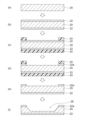
- FIG. FIG. 3 is a process flow chart showing the first half of the manufacturing procedure of EUV transmissive films in Examples 1 to 3.
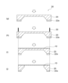
- FIG. 3 is a process flow diagram showing the second half of the manufacturing procedure of EUV transmissive films in Examples 1 to 3.
- FIG. 1 shows a schematic cross-sectional view of an EUV transmissive film 10 according to one embodiment of the present invention.
- the EUV transmissive film 10 includes a main layer 12 and a protective layer 14 covering at least one side of the main layer 12 .
- the main layer 12 is composed of beryllium metal
- the protective layer 14 is composed of beryllium nitride.
- a practical level of high EUV transmittance for example, 91% or more
- a low-pressure hydrogen atmosphere environment can be achieved. It is possible to provide the EUV transmissive film 10 that has both durability and durability.
- the poly-Si-based pellicle film as disclosed in Patent Document 1 cannot reach the target 90% EUV transmittance when the thickness is set to maintain the film strength, and it is still practical. not targeted.
- the CNT-based pellicle film disclosed in Patent Document 2 does not have durability against the pellicle usage environment (low-pressure hydrogen atmosphere). As a result, it becomes impossible to achieve a practical level of transmittance.
- Patent document 1 discloses forming a Ru layer as a protective layer, but although Ru has a high EUV transmittance, when the thickness is 3 nm, the EUV transmittance drops to 90% only with Ru. This reduces the throughput of the EUV exposure process.
- the protective layer 14 used in the present invention is composed of beryllium nitride, thereby providing the main layer 12 with durability in a low-pressure hydrogen atmosphere environment and exhibiting a higher EUV transmittance than the Ru layer.
- the main layer 12 and the protective layer 14 it is possible to provide an EUV permeable film 10 that has both a practically high level of EUV transmittance (for example, 91% or more) and durability in a low-pressure hydrogen atmosphere environment. can be done.
- the main layer 12 is composed of metallic beryllium. However, it is not necessary for the main layer 12 to consist entirely of metallic beryllium. It may be composed of beryllium. While ensuring the basic functions of a pellicle film (particle adhesion prevention function, etc.), it contributes to the realization of a practically high level of EUV transmittance. From this point of view, the thickness of the main layer 12 is preferably 10-70 nm, more preferably 15-50 nm, and still more preferably 20-35 nm.
- the protective layer 14 is a layer for protecting the main layer 12, which is a metallic beryllium layer. Therefore, the protective layer 14 may cover at least one surface of the main layer 12, but it is preferable to cover both surfaces of the main layer 12 with the protective layer.
- the protective layer 14 is composed of beryllium nitride.
- the main layer 12 does not have to consist entirely of beryllium nitride, and 99% by weight or more, preferably 99.5% by weight or more, and more preferably 99.8% by weight or more of the main layer 12 is composed of beryllium nitride. It is good if it is.
- the EUV transmittance is higher than that of a beryllium film having a Ru layer when compared at the same thickness. According to theoretical calculations, the transmittance is 85.8% when a 3-nm-thick Ru film is formed on both sides of a 30-nm-thick beryllium film. beryllium nitride is formed, the transmittance is 91.1%. When a 2-nm-thick beryllium nitride layer and a 1-nm-thick gradient composition layer (a layer composed of a nitrogen concentration gradient region described later) are formed on both sides of a 30-nm-thick beryllium film, the transmittance is 91.1%.
- beryllium is a highly reactive material, so it is easily oxidized to form beryllium oxide, but the oxidation can be suppressed by forming beryllium nitride.
- the advantages of using the beryllium nitride layer as the protective layer 14 as described above are increased EUV transmittance, protection of the beryllium film (main layer 12) during the etching process, and prevention of oxidation.
- the thickness of the protective layer 14 is preferably 5 nm or less, more preferably 3 nm or less.
- the beryllium nitride film with a thickness of 3 nm has an EUV transmittance of 95%, which is much higher than the 90% of the Ru film.
- the lower limit of the thickness of the protective layer 14 is not particularly limited, it is typically 1 nm or more.
- the term "beryllium nitride" includes not only stoichiometric compositions such as Be 3 N 2 but also non-stoichiometric compositions such as Be 3 N 2-x (where 0 ⁇ x ⁇ 2). It is intended to mean a generic composition that also allows stoichiometric compositions.
- Protective layer 14 preferably has a nitrogen concentration gradient region in which the nitrogen concentration decreases as it approaches main layer 12 . That is, as described above, the composition of beryllium nitride forming the protective layer 14 varies from a stoichiometric composition such as Be 3 N 2 to a non-stoichiometric composition such as Be 3 N 2-x (where 0 ⁇ x ⁇ 2). Although the stoichiometric composition can be included, it is preferable that the beryllium nitride constituting the protective layer 14 has a graded composition approaching a beryllium-rich composition as it approaches the main layer 12 .
- the thickness of the nitrogen concentration gradient region is preferably smaller than the thickness of the protective layer 14 . That is, the entire thickness of the protective layer 14 need not be the nitrogen concentration gradient region. For example, only part of the thickness of the protective layer 14, for example, preferably 10 to 70% of the thickness of the protective layer 14, more preferably 15 to 50%, is the nitrogen concentration gradient region. preferable.
- the EUV transmissive film 10 is preferably in the form of a self-supporting film in a main area for transmitting EUV. That is, it is preferable that the substrate (e.g., Si substrate) used for film formation remains as a border only at the outer edge of the EUV transmissive film 10. In other words, the substrate (e.g., Si substrate) does not remain, that is, the main region preferably consists of the main layer 12 and the protective layer 14 only.
- the substrate e.g., Si substrate
- the EUV transmissive film 10 can have a practically high EUV transmittance, preferably 91% or more, more preferably 92% or more, and even more preferably 93% or more. Since a higher EUV transmittance is more desirable, the upper limit is not particularly limited. can be 95% or less.
- the EUV-transmitting film according to the present invention can be manufactured by forming a laminated film to be an EUV-transmitting film on a Si substrate and then removing unnecessary portions of the Si substrate by etching to form a self-supporting film. Therefore, as described above, the main part of the EUV transmissive film is in the form of a self-supporting film in which the Si substrate does not remain.
- Preparation of Si substrate First, prepare a Si substrate for forming a laminated film thereon. After the laminated film consisting of the main layer 12 and the protective layer 14 is formed on the Si substrate, the main region (that is, the region to be a self-supporting film) other than the outer edge is removed by etching. Therefore, in order to perform etching efficiently in a short time, it is desirable to reduce the thickness of the Si substrate in the region to be the self-supporting film in advance. Therefore, using a normal semiconductor process, a mask corresponding to the EUV transmission shape is formed on the Si substrate, and the Si substrate is etched by wet etching to reduce the thickness of the main region of the Si substrate to a predetermined thickness. desired.
- a Si substrate having a cavity formed by wet etching is prepared.
- the wet etching mask any material having corrosion resistance to the wet etching solution for Si may be used.
- SiO 2 is preferably used.
- the wet etching liquid is not particularly limited as long as it can etch Si.
- TMAH tetramethylammonium hydroxide
- (2) Formation of laminated film Formation of the laminated film may be performed by any film forming method.
- Sputtering method is mentioned as an example of the preferable film-forming method.
- the beryllium film as the main layer 12 is fabricated by sputtering using a pure Be target, and the beryllium nitride film as the protective layer 14 is fabricated by reactive sputtering. preferably done.
- This reactive sputtering can be carried out, for example, by introducing nitrogen gas into the chamber during sputtering using a pure Be target, so that beryllium reacts with nitrogen to produce beryllium nitride.
- beryllium nitride can be produced by forming a beryllium film and then irradiating nitrogen plasma to cause a nitridation reaction of beryllium to produce beryllium nitride.
- the method for synthesizing beryllium nitride is not limited to these.
- it is preferable to use different beryllium targets for forming the beryllium nitride film and beryllium targets for forming the beryllium film it is also possible to use the same target for forming the beryllium nitride film and for forming the beryllium film. .
- beryllium nitride film and the beryllium film may be formed in a single-chamber sputtering apparatus as in the examples described later, or the beryllium nitride film and the beryllium film may be formed in separate chambers using a two-chamber sputtering apparatus. may be formed.
- the introduction of the nitrogen gas may be stopped halfway and the film of beryllium metal may be switched to the film while continuing the sputtering. .
- a region is formed in which the nitrogen concentration in the film to be formed decreases in the thickness direction as the nitrogen gas concentration decreases.
- the nitrogen concentration gradient region can be formed by starting the introduction of nitrogen gas halfway while continuing the sputtering, contrary to the above.
- the thickness of the nitrogen concentration gradient region can be controlled by adjusting the time for changing the nitrogen gas concentration.
- the composite film is formed into a self-supporting film by removing unnecessary portions of the Si substrate other than the outer edge portion left as a border of the Si substrate on which the composite film is formed by etching.
- Etching of Si may be performed by any method, but etching using XeF 2 is preferably performed.
- Example 1 According to the procedure shown in FIGS. 2A and 2B, a composite self-supporting film (EUV transmissive film) having a three-layer structure of beryllium nitride/beryllium/beryllium nitride was produced as follows.
- EUV transmissive film EUV transmissive film
- the resist mask 24 for SiO2 etching was removed by an ashing device (FIG. 2A(e)).
- Si was etched with a TMAH solution.
- the etching rate was measured in advance, and the etching was performed for the etching time required to obtain the target Si substrate thickness of 50 ⁇ m (FIG. 2A(f)).
- the SiO 2 film 22 formed on the non-Si-etched surface was removed and washed with hydrofluoric acid to prepare a Si substrate 28 (FIG. 2B(g)).
- the outer shape of the Si substrate may be diced with a laser 30 as necessary (FIG. 2B(h)) to obtain a desired shape (FIG. 2B(i)).
- a cavity 26 of 110 mm ⁇ 145 mm was provided in the center of the 8-inch (20.32 cm) Si wafer 20, and a Si substrate 28 having a Si thickness of 50 ⁇ m at the cavity 26 portion was prepared.
- a composite film having a three-layer structure of beryllium nitride/beryllium/beryllium nitride was formed as follows on the Si substrate 28 provided with the cavity 26 obtained in (1) above (Fig. 2B (i)).
- the Si substrate 28 was set in a sputtering apparatus, and a pure Be target was attached.
- the inside of the chamber was evacuated, the internal pressure was 0.5 Pa, and reactive sputtering was performed by adjusting the flow rate ratio of argon gas and nitrogen gas to be 1:1. bottom.
- sputtering was performed using only argon gas without introducing nitrogen gas, and the sputtering was terminated after a time was taken to deposit 25 nm of beryllium.
- the Si substrate 28 with the composite film prepared in (2) above was set in a chamber of a XeF 2 etcher capable of processing an 8-inch (20.32 cm) substrate.
- the inside of the chamber was sufficiently evacuated. At this time, if moisture remains in the chamber, it reacts with the XeF 2 gas to produce hydrofluoric acid, which corrodes the etcher and causes unexpected etching. If necessary, the inside of the chamber was repeatedly evacuated and introduced with nitrogen gas to reduce residual moisture. When the vacuum was sufficiently drawn, the valve between the XeF 2 raw material cylinder and the preliminary chamber was opened. As a result, XeF 2 was sublimated and XeF 2 gas was accumulated in the preliminary chamber.
- Example 2 A composite self-supporting film was produced in the same manner as in Example 1, except that the composite film was formed as follows.
- Example 1 (1) (Formation of composite membrane) The Si substrate having the cavity formed in Example 1 (1) was placed in a sputtering apparatus, and beryllium was deposited to a thickness of 1 nm. By generating plasma while introducing nitrogen gas into the chamber, the generated nitrogen plasma was reacted with the formed beryllium film to form beryllium nitride. Next, a beryllium film was formed to a thickness of 26 nm on the formed beryllium nitride film, and after the film formation, plasma was generated while nitrogen gas was introduced into the chamber again, and the surface was changed to beryllium nitride.
- a 25 nm-thick beryllium film (composite film of 1.5 nm beryllium nitride/25 nm beryllium/1.5 nm beryllium nitride) having 1.5 nm-thick beryllium nitride films on both sides was formed.
- Example 3 (Comparison) EUV transmission was performed in the same manner as in Example 1, except that no beryllium nitride film was formed (that is, a single layer film of beryllium 25 nm was formed instead of a composite film of beryllium nitride 2 nm/beryllium 25 nm/beryllium nitride 2 nm). A film (beryllium single-layer free-standing film) was produced.
- EUV transmittance The EUV transmittance films produced in Examples 1 to 3 were irradiated with EUV light, and the amount of transmitted EUV light was measured with a sensor. The EUV transmittance was obtained from a comparison between the obtained measured value and the value obtained by directly measuring the amount of EUV light with a sensor without the EUV transmissive film. As a result, the EUV transmittance of the composite self-supporting film produced in Example 1 was 93.0%, which was almost the same as the theoretically calculated value of 93.3%. Moreover, the EUV transmittance of the composite self-supporting film produced in Example 2 was 93.5%, which is close to the theoretically calculated value of 94.1%.
Landscapes
- Physics & Mathematics (AREA)
- General Physics & Mathematics (AREA)
- Optics & Photonics (AREA)
- Preparing Plates And Mask In Photomechanical Process (AREA)
- Laminated Bodies (AREA)
- Optical Filters (AREA)
- Physical Vapour Deposition (AREA)
Abstract
実用レベルの高いEUV透過率と、低圧水素雰囲気環境における耐久性とを兼ね備えた、EUV透過膜が提供される。このEUV透過膜は、金属ベリリウムで構成される主層と、主層の少なくとも片面を覆う、窒化べリリウムで構成される保護層とを備える。
Description
本発明は、EUV透過膜に関するものである。
半導体製造プロセスにおける微細化が年々進行しており、各工程で様々な改良がなされている。特に、フォトリソグラフィ工程においては、従来のArF露光の波長193nmに代えて、波長13.5nmのEUV(極端紫外線)光が使用され始めた。その結果、波長が一気に1/10以下になり、その光学的特性は全く異なるものとなった。しかし、EUV光に対して高透過率を有する物質が無いため、例えばフォトマスク(レチクル(reticle))のパーティクル付着防止膜であるペリクル(pellicle)にはまだ実用的な物が存在しない。このため、デバイスメーカーはペリクルを使うことができずに半導体デバイスの製造を行っているのが現状である。
そこで、ポリSiベースのペリクル膜が提案されている。例えば、特許文献1(特許第6858817号公報)には、コア層が(ポリ)Si等のEUV放射に実質的に透明な材料を含むコア層と、IR放射を吸収する材料を含むキャップ層とを備えたペリクル膜が開示されている。しかしながら、ポリSiベースのペリクル膜は、膜強度を保持するための厚さとした場合、EUV透過率は目標の90%に到達できず、いまだ実用的ではない。
また、カーボンナノチューブ(CNT)ベースのペリクル膜も開発されており(例えば特許文献2(特開2018-194840号公報))、より高いEUV透過率が期待される。
しかしながら、CNTベースのペリクル膜ではペリクル使用環境(低圧水素雰囲気)に対する耐久性が無く、耐久性を持たせるためにペリクル膜に金属を被覆すると、EUV透過率が低下してしまい実用レベルの透過率を達成できなくなるのが実情である。そこで、実用レベルの高いEUV透過率を有しながらも、低圧水素雰囲気環境における耐久性をも有する、EUV透過膜が望まれる。
本発明者らは、今般、金属ベリリウムで構成される主層と、窒化べリリウムで構成される保護層とを組み合わせることで、実用レベルの高いEUV透過率と、低圧水素雰囲気環境における耐久性とを兼ね備えた、EUV透過膜を提供できるとの知見を得た。
したがって、本発明の目的は、実用レベルの高いEUV透過率と、低圧水素雰囲気環境における耐久性とを兼ね備えた、EUV透過膜を提供することにある。
本発明の一態様によれば、
金属ベリリウムで構成される主層と、
前記主層の少なくとも片面を覆う、窒化べリリウムで構成される保護層と、
を備えた、EUV透過膜が提供される。
金属ベリリウムで構成される主層と、
前記主層の少なくとも片面を覆う、窒化べリリウムで構成される保護層と、
を備えた、EUV透過膜が提供される。
EUV透過膜
図1に本発明の一形態によるEUV透過膜10の模式断面図を示す。EUV透過膜10は、主層12と、主層12の少なくとも片面を覆う保護層14とを備える。主層12は金属ベリリウムで構成される一方、保護層14は窒化べリリウムで構成される。このように、金属ベリリウムで構成される主層12と、窒化べリリウムで構成される保護層14とを組み合わせることで、実用レベルの高いEUV透過率(例えば91%以上)と、低圧水素雰囲気環境における耐久性とを兼ね備えた、EUV透過膜10を提供することができる。
図1に本発明の一形態によるEUV透過膜10の模式断面図を示す。EUV透過膜10は、主層12と、主層12の少なくとも片面を覆う保護層14とを備える。主層12は金属ベリリウムで構成される一方、保護層14は窒化べリリウムで構成される。このように、金属ベリリウムで構成される主層12と、窒化べリリウムで構成される保護層14とを組み合わせることで、実用レベルの高いEUV透過率(例えば91%以上)と、低圧水素雰囲気環境における耐久性とを兼ね備えた、EUV透過膜10を提供することができる。
すなわち、前述のとおり、特許文献1に開示されるようなポリSiベースのペリクル膜は、膜強度を保持するための厚さとした場合、EUV透過率は目標の90%に到達できず、いまだ実用的ではない。一方、特許文献2に開示されるようなCNTベースのペリクル膜ではペリクル使用環境(低圧水素雰囲気)に対する耐久性が無く、耐久性を持たせるためにペリクル膜に金属を被覆すると、EUV透過率が低下してしまい実用レベルの透過率を達成できなくなる。これらの問題が、本発明のEUV透過膜10によれば首尾よく解決される。このことは以下のように説明することできる。まず、主層12は金属ベリリウムで構成される。ベリリウムはSiやCよりも高いEUV透過率を有しているため、実用レベルの高いEUV透過率(例えば91%以上)を呈する。一方、ベリリウムは、反応性が高い物質であるため、ペリクル膜の作製中に他の材料と反応したり、ペリクル膜の作製後に酸化して酸化ベリリウムを生成し、それによりEUV透過率が低下してしまう。そのため主層12に保護層14を設けることで、主層12中のベリリウムの反応を防止することができる。特許文献1には保護層としてRu層を形成することが開示されているが、RuのEUV透過率が高いとはいえ、厚さ3nmにするとRuだけでEUV透過率が90%まで低下してしまい、EUV露光プロセスの処理能力を低下させてしまう。この点、本発明に用いる保護層14は、窒化べリリウムで構成されることで、低圧水素雰囲気環境における耐久性を主層12にもたらすとともに、Ru層よりも高いEUV透過率を呈する。その結果、主層12及び保護層14を組み合わせることで、実用レベルの高いEUV透過率(例えば91%以上)と、低圧水素雰囲気環境における耐久性とを兼ね備えた、EUV透過膜10を提供することができる。
主層12は、金属ベリリウムで構成される。もっとも、主層12が完全に金属ベリリウムで構成される必要はなく、主層12の好ましくは99重量%以上、より好ましくは99.5重量%以上、さらに好ましくは99.8重量%以上が金属ベリリウムで構成されていればよい。ペリクル膜としての基本的機能(パーティクル付着防止機能等)を確保しながら、実用レベルの高いEUV透過率の実現に寄与する。かかる観点から、主層12の厚さは、10~70nmであるのが好ましく、より好ましくは15~50nm、さらに好ましくは20~35nmである。
保護層14は、金属ベリリウム層である主層12を保護するための層である。したがって、保護層14は、主層12の少なくとも片面を覆っていればよいが、主層12の両面を保護層で覆うのが好ましい。保護層14は、窒化べリリウムで構成される。もっとも、主層12が完全に窒化ベリリウムで構成される必要はなく、主層12の99重量%以上、好ましくは99.5重量%以上、さらに好ましくは99.8重量%以上が窒化ベリリウムで構成されていればよい。窒化ベリリウムはEUV透過率が高いため、同じ厚さで比較するとRu層を形成したベリリウム膜よりもEUV透過率は高くなる。理論計算によると、厚さ30nmのベリリウム膜の両面に、厚さ3nmのRu膜を形成した場合の透過率は85.8%であるが、厚さ30nmのベリリウム膜の両面に、厚さ3nmの窒化ベリリウムを形成した場合の透過率は91.1%となる。厚さ30nmのベリリウム膜の両面に、厚さ2nmの窒化ベリリウムと厚さ1nmの傾斜組成層(後述する窒素濃度傾斜領域で構成される層)を形成した場合の透過率は91.1%を越える。ベリリウム層の両面に緻密な窒化ベリリウム層を形成することにより、後述するSi基板のエッチングに用いられるXeF2ガスとの反応を抑制できる。また、ベリリウムは非常に反応性の高い材料のため、容易に酸化して酸化ベリリウムを形成するが、窒化ベリリウムの形成で酸化を抑制可能である。上記のとおり窒化ベリリウム層を保護層14として用いることのメリットは、EUV透過率の増大、エッチングプロセスにおけるベリリウム膜(主層12)の保護、及び酸化防止である。
保護層14の厚さは5nm以下であるのが好ましく、より好ましくは3nm以下である。厚さ3nmの窒化ベリリウム膜ではEUV透過率が95%と、Ru膜の90%よりも格段に高い。保護層14の厚さの下限値は特に限定されないが、典型的には1nm以上である。なお、本明細書において「窒化ベリリウム」なる用語は、Be3N2のような化学量論組成のみならず、Be3N2-x(式中0<x<2である)のような非化学量論組成も許容する包括的な組成を意味するものとする。
保護層14は、主層12に近づくにつれて窒素濃度が減少する窒素濃度傾斜領域を有するのが好ましい。すなわち、上述のとおり保護層14を構成する窒化ベリリウムの組成にはBe3N2のような化学量論組成からBe3N2-x(式中0<x<2である)のような非化学量論組成まで包含しうるところ、保護層14を構成する窒化ベリリウムが、主層12に近づくにつれてベリリウムリッチの組成に近づく傾斜組成とするのが好ましい。こうすることで、保護層14(すなわち窒化ベリリウム層)と主層12(すなわち金属ベリリウム層)との密着性を向上できるとともに、両層間の熱膨張差に起因する応力の発生を緩和することができる。すなわち、両層間の密着性を向上させて剥離を抑制したり、EUV光を吸収して高温になった場合の両層間の熱膨張緩和層として剥離しにくくしたりすることができる。窒素濃度傾斜領域の厚さは、保護層14の厚さよりも小さいのが好ましい。すなわち、保護層14の厚さの全域が窒素濃度傾斜領域である必要はない。例えば、保護層14の厚さの一部のみ、例えば、保護層14の厚さのうち好ましくは10~70%の領域、より好ましくは15~50%の領域が窒素濃度傾斜領域であるのが好ましい。
EUV透過膜10は、EUVを透過するための主要領域が自立膜の形態であるのが好ましい。すなわち、EUV透過膜10の外縁部にのみ、成膜時に用いた基板(例えばSi基板)がボーダー(border)として残存しているのが好ましい、つまり、外縁部以外の主要領域には基板(例えばSi基板)が残存していない、すなわち主要領域は主層12及び保護層14のみで構成されるのが好ましい。
EUV透過膜10は、実用レベルの高いEUV透過率を有することができ、好ましくは91%以上、より好ましくは92%以上、さらに好ましくは93%以上のEUV透過率を有する。EUV透過率は高ければ高いほど望ましいため、上限値は特に限定されないが、EUV透過膜10のEUV透過率は、典型的には99%以下、より典型的には98%以下、さらに典型的には95%以下でありうる。
製造方法
本発明によるEUV透過膜は、Si基板上にEUV透過膜とすべき積層膜を形成した後、Si基板の不要部分をエッチングで除去して自立膜化することにより作製することができる。したがって、前述のとおり、EUV透過膜の主要部分はSi基板が残存していない自立膜の形態となっている。
本発明によるEUV透過膜は、Si基板上にEUV透過膜とすべき積層膜を形成した後、Si基板の不要部分をエッチングで除去して自立膜化することにより作製することができる。したがって、前述のとおり、EUV透過膜の主要部分はSi基板が残存していない自立膜の形態となっている。
(1)Si基板の準備
まず、その上に積層膜を形成するためのSi基板を準備する。Si基板は、その上に主層12と保護層14からなる積層膜を形成した後に、その外縁部以外の主要領域(すなわち自立膜とすべき領域)がエッチングにより除去されることになる。したがって、エッチングを効率良く短時間で行うため、予め自立膜とすべき領域のSi基板の厚さを薄くしておくことが望ましい。そのため、通常の半導体プロセスを用いて、Si基板にEUV透過形状に対応したマスクを形成し、ウェットエッチングによりSi基板をエッチングして、Si基板の主要領域の厚さを所定厚さまで薄くすることが望まれる。ウェットエッチングを経たSi基板を洗浄及び乾燥することで、ウェットエッチングにより形成したキャビティを有するSi基板を準備する。なお、ウェットエッチングマスクとしては、Siのウェットエッチング液に対して耐食性を有する材質であればよく、例えばSiO2が好適に使用される。また、ウェットエッチング液としては、Siをエッチング可能なものであれば特に限定されない。例えば、TMAH(水酸化テトラメチルアンモニウム)を適切な条件で使用すれば、Siに対する異方性エッチングで非常に良好なエッチングができるため好ましい。
まず、その上に積層膜を形成するためのSi基板を準備する。Si基板は、その上に主層12と保護層14からなる積層膜を形成した後に、その外縁部以外の主要領域(すなわち自立膜とすべき領域)がエッチングにより除去されることになる。したがって、エッチングを効率良く短時間で行うため、予め自立膜とすべき領域のSi基板の厚さを薄くしておくことが望ましい。そのため、通常の半導体プロセスを用いて、Si基板にEUV透過形状に対応したマスクを形成し、ウェットエッチングによりSi基板をエッチングして、Si基板の主要領域の厚さを所定厚さまで薄くすることが望まれる。ウェットエッチングを経たSi基板を洗浄及び乾燥することで、ウェットエッチングにより形成したキャビティを有するSi基板を準備する。なお、ウェットエッチングマスクとしては、Siのウェットエッチング液に対して耐食性を有する材質であればよく、例えばSiO2が好適に使用される。また、ウェットエッチング液としては、Siをエッチング可能なものであれば特に限定されない。例えば、TMAH(水酸化テトラメチルアンモニウム)を適切な条件で使用すれば、Siに対する異方性エッチングで非常に良好なエッチングができるため好ましい。
(2)積層膜の形成
積層膜の形成は、いかなる成膜手法により行われてもよい。好ましい成膜手法の一例としては、スパッタリング法が挙げられる。窒化ベリリウム/ベリリウム/窒化ベリリウムの3層構造を作製する場合、主層12としてのベリリウム膜は、純Beターゲットを用いたスパッタリングにより作製し、保護層14としての窒化ベリリウム膜は、反応性スパッタリングにより行うのが好ましい。この反応性スパッタリングは、例えば、純Beターゲットを用いたスパッタリング中に、チャンバー内に窒素ガスを入れることで、ベリリウムと窒素が反応して窒化ベリリウムを生成することにより行うことができる。また、別の手法として、窒化ベリリウムの作製は、ベリリウム膜を形成した後、窒素プラズマを照射することでベリリウムを窒化反応させて窒化ベリリウムを生成させることにより行うこともできる。いずれにしても、窒化ベリリウムの合成手法はこれらに限定されるものではない。なお、窒化ベリリウム膜形成用のベリリウムターゲットと、ベリリウム膜形成用のベリリウムターゲットは、別々のものを用いるのが好ましいが、窒化ベリリウム膜形成とベリリウム膜形成で同一のターゲットを用いることも可能である。なお、窒化ベリリウム膜とベリリウム膜は後述する実施例のように1つのチャンバーのスパッタリング装置で形成してもよいし、2チャンバーのスパッタリング装置を用いて窒化ベリリウム膜とベリリウム膜を別々のチャンバー内で形成してもよい。
積層膜の形成は、いかなる成膜手法により行われてもよい。好ましい成膜手法の一例としては、スパッタリング法が挙げられる。窒化ベリリウム/ベリリウム/窒化ベリリウムの3層構造を作製する場合、主層12としてのベリリウム膜は、純Beターゲットを用いたスパッタリングにより作製し、保護層14としての窒化ベリリウム膜は、反応性スパッタリングにより行うのが好ましい。この反応性スパッタリングは、例えば、純Beターゲットを用いたスパッタリング中に、チャンバー内に窒素ガスを入れることで、ベリリウムと窒素が反応して窒化ベリリウムを生成することにより行うことができる。また、別の手法として、窒化ベリリウムの作製は、ベリリウム膜を形成した後、窒素プラズマを照射することでベリリウムを窒化反応させて窒化ベリリウムを生成させることにより行うこともできる。いずれにしても、窒化ベリリウムの合成手法はこれらに限定されるものではない。なお、窒化ベリリウム膜形成用のベリリウムターゲットと、ベリリウム膜形成用のベリリウムターゲットは、別々のものを用いるのが好ましいが、窒化ベリリウム膜形成とベリリウム膜形成で同一のターゲットを用いることも可能である。なお、窒化ベリリウム膜とベリリウム膜は後述する実施例のように1つのチャンバーのスパッタリング装置で形成してもよいし、2チャンバーのスパッタリング装置を用いて窒化ベリリウム膜とベリリウム膜を別々のチャンバー内で形成してもよい。
窒素濃度傾斜領域を形成する場合、窒化ベリリウムの成膜から金属ベリリウムの成膜を行うに際して、スパッタリングを継続して行いながら、途中から窒素ガスの導入を止めて金属ベリリウムの成膜に切り替えればよい。こうすることで、窒素ガスの濃度の低下に伴い、成膜される膜中の窒素濃度が厚さ方向に減少する領域が形成される。一方、金属ベリリウムから窒化ベリリウムに切り替える場合は、上記とは逆に、スパッタリングを継続して行いながら、途中から窒素ガスの導入を始めれば、窒素濃度傾斜領域を形成することができる。窒素濃度傾斜領域の厚さは、窒素ガス濃度を変化させる時間を調整することにより制御することができる。
(3)自立膜化
複合膜を形成したSi基板の、ボーダー(border)として残す外縁部以外のSi基板の不要部分をエッチングで除去して、複合膜の自立膜化を行う。Siのエッチングは、いかなる手法により行われてもよいが、XeF2を用いたエッチングにより好ましく行うことができる。
複合膜を形成したSi基板の、ボーダー(border)として残す外縁部以外のSi基板の不要部分をエッチングで除去して、複合膜の自立膜化を行う。Siのエッチングは、いかなる手法により行われてもよいが、XeF2を用いたエッチングにより好ましく行うことができる。
本発明を以下の例によってさらに具体的に説明する。
例1
図2A及び2Bに示される手順に従い、窒化ベリリウム/ベリリウム/窒化ベリリウムの3層構造の複合自立膜(EUV透過膜)を以下のようにして作製した。
図2A及び2Bに示される手順に従い、窒化ベリリウム/ベリリウム/窒化ベリリウムの3層構造の複合自立膜(EUV透過膜)を以下のようにして作製した。
(1)Si基板の準備
直径8インチ(20.32cm)のSiウェハ20を用意した(図2A(a))。このSiウェハ20の両面に、熱酸化によりSiO2膜22を50nm厚さで形成した(図2A(b))。Siウェハ20の両面にレジストを塗布し、片面に110mm×145mmのレジストの穴ができるように、露光及び現像を行いSiO2エッチング用のレジストマスク24を形成した(図2A(c))。この基板の一方の面をフッ酸でウェットエッチングすることにより、SiO2膜22の露出部分をエッチング除去してSiO2マスク22aを作製した(図2A(d))。SiO2エッチングのためのレジストマスク24をアッシング装置で除去した(図2A(e))。その後、TMAH液によりSiをエッチングした。このエッチングは、事前にエッチングレートを測定しておき、狙いとするSi基板厚50μmとするためのエッチング時間だけ実施した(図2A(f))。最後にSiエッチングしていない面に形成してあるSiO2膜22をフッ酸により除去及び洗浄して、Si基板28を準備した(図2B(g))。Si基板外形は必要に応じてレーザー30でダイシングして(図2B(h))、所望の形状としてもよい(図2B(i))。こうして、8インチ(20.32cm)Siウェハ20の中央に110mm×145mmのキャビティ26を設け、キャビティ26部分のSi厚さが50μmであるSi基板28を準備した。
直径8インチ(20.32cm)のSiウェハ20を用意した(図2A(a))。このSiウェハ20の両面に、熱酸化によりSiO2膜22を50nm厚さで形成した(図2A(b))。Siウェハ20の両面にレジストを塗布し、片面に110mm×145mmのレジストの穴ができるように、露光及び現像を行いSiO2エッチング用のレジストマスク24を形成した(図2A(c))。この基板の一方の面をフッ酸でウェットエッチングすることにより、SiO2膜22の露出部分をエッチング除去してSiO2マスク22aを作製した(図2A(d))。SiO2エッチングのためのレジストマスク24をアッシング装置で除去した(図2A(e))。その後、TMAH液によりSiをエッチングした。このエッチングは、事前にエッチングレートを測定しておき、狙いとするSi基板厚50μmとするためのエッチング時間だけ実施した(図2A(f))。最後にSiエッチングしていない面に形成してあるSiO2膜22をフッ酸により除去及び洗浄して、Si基板28を準備した(図2B(g))。Si基板外形は必要に応じてレーザー30でダイシングして(図2B(h))、所望の形状としてもよい(図2B(i))。こうして、8インチ(20.32cm)Siウェハ20の中央に110mm×145mmのキャビティ26を設け、キャビティ26部分のSi厚さが50μmであるSi基板28を準備した。
(2)複合膜の形成
上記(1)で得られたキャビティ26を備えたSi基板28に、窒化ベリリウム/ベリリウム/窒化ベリリウムの3層構造の複合膜を以下のようにして形成した(図2B(i))。まず、スパッタリング装置にSi基板28をセットし、純Beターゲットを取り付けた。チャンバー内を真空引きし、内圧0.5Paで、アルゴンガスと窒素ガス流量比が1:1となるよう調整し反応性スパッタリングを行い、窒化ベリリウムが2nm積層する時間を見計らって反応性スパッタリングを終了した。次いで、窒素ガスを導入しないで、アルゴンガスのみでスパッタリングを行い、ベリリウムが25nm積層する時間を見計らってスパッタリングを終了した。その後、最初と同様に再度窒素ガスを導入しつつ、反応性スパッタリングを行い、窒化ベリリウムが2nm積層する時間を見計らって反応性スパッタリングを終了した。このようにして、窒化ベリリウム2nm/ベリリウム25nm/窒化ベリリウム2nmの複合膜をEUV透過膜10として形成した。
上記(1)で得られたキャビティ26を備えたSi基板28に、窒化ベリリウム/ベリリウム/窒化ベリリウムの3層構造の複合膜を以下のようにして形成した(図2B(i))。まず、スパッタリング装置にSi基板28をセットし、純Beターゲットを取り付けた。チャンバー内を真空引きし、内圧0.5Paで、アルゴンガスと窒素ガス流量比が1:1となるよう調整し反応性スパッタリングを行い、窒化ベリリウムが2nm積層する時間を見計らって反応性スパッタリングを終了した。次いで、窒素ガスを導入しないで、アルゴンガスのみでスパッタリングを行い、ベリリウムが25nm積層する時間を見計らってスパッタリングを終了した。その後、最初と同様に再度窒素ガスを導入しつつ、反応性スパッタリングを行い、窒化ベリリウムが2nm積層する時間を見計らって反応性スパッタリングを終了した。このようにして、窒化ベリリウム2nm/ベリリウム25nm/窒化ベリリウム2nmの複合膜をEUV透過膜10として形成した。
(3)自立膜化
8インチ(20.32cm)基板を処理可能なXeF2エッチャーのチャンバー内に、上記(2)で準備した複合膜付きのSi基板28をセットした。チャンバー内を十分真空引きした。このとき、チャンバー内に水分が残留していると、XeF2ガスと反応してフッ酸を生じ、エッチャーの腐食や想定外のエッチングが起きてしまうため、十分な真空引きを行った。必要に応じて、チャンバー内を、真空引きと窒素ガス導入を繰り返し、残留水分を減らした。十分に真空引きが出来たところで、XeF2原料ボンベと予備室の間のバルブを開いた。その結果、XeF2が昇華して予備室内にもXeF2ガスが蓄積された。十分に予備室内にXeF2ガスが蓄積されたところで、予備室とチャンバーの間のバルブを開き、XeF2ガスをチャンバー内に導入した。XeF2ガスはXeとFに分解し、FはSiと反応してSiF4を生成した。SiF4の沸点は-95℃であるため、生成したSiF4は速やかに蒸発し、新たに露出したSi基板とFの反応が引き起こされた。Siエッチングが進行し、チャンバー内のFが減少したところで、チャンバー内を真空引きし、再度XeF2ガスをチャンバー内に導入しエッチングを行った。このようにして、真空引き、XeF2ガス導入、及びエッチングを繰り返して、自立膜化させる部分に対応するSi基板28が消失するまでエッチングを続けた。不要部分のSi基板が無くなったところでエッチングを終了した。こうして、Si製ボーダー(border)を有する複合自立膜をEUV透過膜10として得た(図2(j))。
8インチ(20.32cm)基板を処理可能なXeF2エッチャーのチャンバー内に、上記(2)で準備した複合膜付きのSi基板28をセットした。チャンバー内を十分真空引きした。このとき、チャンバー内に水分が残留していると、XeF2ガスと反応してフッ酸を生じ、エッチャーの腐食や想定外のエッチングが起きてしまうため、十分な真空引きを行った。必要に応じて、チャンバー内を、真空引きと窒素ガス導入を繰り返し、残留水分を減らした。十分に真空引きが出来たところで、XeF2原料ボンベと予備室の間のバルブを開いた。その結果、XeF2が昇華して予備室内にもXeF2ガスが蓄積された。十分に予備室内にXeF2ガスが蓄積されたところで、予備室とチャンバーの間のバルブを開き、XeF2ガスをチャンバー内に導入した。XeF2ガスはXeとFに分解し、FはSiと反応してSiF4を生成した。SiF4の沸点は-95℃であるため、生成したSiF4は速やかに蒸発し、新たに露出したSi基板とFの反応が引き起こされた。Siエッチングが進行し、チャンバー内のFが減少したところで、チャンバー内を真空引きし、再度XeF2ガスをチャンバー内に導入しエッチングを行った。このようにして、真空引き、XeF2ガス導入、及びエッチングを繰り返して、自立膜化させる部分に対応するSi基板28が消失するまでエッチングを続けた。不要部分のSi基板が無くなったところでエッチングを終了した。こうして、Si製ボーダー(border)を有する複合自立膜をEUV透過膜10として得た(図2(j))。
例2
複合膜の形成を以下のとおり行ったこと以外は、例1と同様にして複合自立膜を作製した。
複合膜の形成を以下のとおり行ったこと以外は、例1と同様にして複合自立膜を作製した。
(複合膜の形成)
例1の(1)で得られたキャビティを形成したSi基板を、スパッタリング装置内に入れ、ベリリウムを1nmの厚さに成膜した。そして、チャンバー内に窒素ガスを導入しつつプラズマを発生させることで、発生した窒素プラズマを成膜したベリリウムと反応させて窒化ベリリウムを形成させた。次いで、形成した窒化ベリリウム膜上にベリリウムを26nmの厚さに成膜し、成膜後に再度チャンバー内に窒素ガスを導入しつつプラズマを発生させ、表面を窒化ベリリウムにした。こうして、両側に厚さ1.5nmの窒化ベリリウム膜を有する厚さ25nmのベリリウム膜(窒化ベリリウム1.5nm/ベリリウム25nm/窒化ベリリウム1.5nmの複合膜)を形成した。
例1の(1)で得られたキャビティを形成したSi基板を、スパッタリング装置内に入れ、ベリリウムを1nmの厚さに成膜した。そして、チャンバー内に窒素ガスを導入しつつプラズマを発生させることで、発生した窒素プラズマを成膜したベリリウムと反応させて窒化ベリリウムを形成させた。次いで、形成した窒化ベリリウム膜上にベリリウムを26nmの厚さに成膜し、成膜後に再度チャンバー内に窒素ガスを導入しつつプラズマを発生させ、表面を窒化ベリリウムにした。こうして、両側に厚さ1.5nmの窒化ベリリウム膜を有する厚さ25nmのベリリウム膜(窒化ベリリウム1.5nm/ベリリウム25nm/窒化ベリリウム1.5nmの複合膜)を形成した。
例3(比較)
窒化ベリリウム膜を形成しなかったこと(すなわち窒化ベリリウム2nm/ベリリウム25nm/窒化ベリリウム2nmの複合膜の代わりに、ベリリウム25nmの単層膜を形成したこと)以外は、例1と同様にしてEUV透過膜(ベリリウム単層自立膜)を作製した。
窒化ベリリウム膜を形成しなかったこと(すなわち窒化ベリリウム2nm/ベリリウム25nm/窒化ベリリウム2nmの複合膜の代わりに、ベリリウム25nmの単層膜を形成したこと)以外は、例1と同様にしてEUV透過膜(ベリリウム単層自立膜)を作製した。
EUV透過率
例1~3で作製したEUV透過膜にEUV光を照射して、透過したEUV光量をセンサーで測定した。得られた測定値と、EUV透過膜無しで直接のEUV光量をセンサーで測定した値との比較から、EUV透過率を求めた。その結果、例1で作製した複合自立膜のEUV透過率は93.0%であり、理論計算値の93.3%とほぼ同等の結果であった。また、例2で作製した複合自立膜のEUV透過率は93.5%であり、理論計算値の94.1%に近い値が得られた。これらの実測値と理論値の差は、膜厚の誤差によるものと推測される。一方、比較例である例3のベリリウム単層自立膜のEUV透過率を測定したところ、90.2%であった。この単層自立膜を解析したところ、両表面にはXeF2エッチングの際に形成したと考えられるフッ化ベリリウムが確認された。このフッ化ベリリウムによりEUV透過率が低下したものと考えられる。
例1~3で作製したEUV透過膜にEUV光を照射して、透過したEUV光量をセンサーで測定した。得られた測定値と、EUV透過膜無しで直接のEUV光量をセンサーで測定した値との比較から、EUV透過率を求めた。その結果、例1で作製した複合自立膜のEUV透過率は93.0%であり、理論計算値の93.3%とほぼ同等の結果であった。また、例2で作製した複合自立膜のEUV透過率は93.5%であり、理論計算値の94.1%に近い値が得られた。これらの実測値と理論値の差は、膜厚の誤差によるものと推測される。一方、比較例である例3のベリリウム単層自立膜のEUV透過率を測定したところ、90.2%であった。この単層自立膜を解析したところ、両表面にはXeF2エッチングの際に形成したと考えられるフッ化ベリリウムが確認された。このフッ化ベリリウムによりEUV透過率が低下したものと考えられる。
Claims (7)
- 金属ベリリウムで構成される主層と、
前記主層の少なくとも片面を覆う、窒化べリリウムで構成される保護層と、
を備えた、EUV透過膜。 - 前記主層の両面が前記保護層で覆われている、請求項1に記載のEUV透過膜。
- 前記保護層の厚さが5nm以下である、請求項1又は2に記載のEUV透過膜。
- 前記保護層の厚さが3nm以下である、請求項1~3のいずれか一項に記載のEUV透過膜。
- 前記保護層が、前記主層に近づくにつれて窒素濃度が減少する窒素濃度傾斜領域を有する、請求項1~4のいずれか一項に記載のEUV透過膜。
- 前記窒素濃度傾斜領域の厚さが、前記保護層の厚さよりも小さい、請求項5に記載のEUV透過膜。
- 前記主層の厚さが、10~70nmである、請求項1~6のいずれか一項に記載のEUV透過膜。
Priority Applications (15)
| Application Number | Priority Date | Filing Date | Title |
|---|---|---|---|
| KR1020237002844A KR102891816B1 (ko) | 2021-10-20 | 2021-10-20 | Euv 투과막 |
| JP2023507498A JP7492649B2 (ja) | 2021-10-20 | 2021-10-20 | Euv透過膜 |
| CN202180055382.6A CN118076920A (zh) | 2021-10-20 | 2021-10-20 | Euv透过膜 |
| EP21954413.7A EP4194948A4 (en) | 2021-10-20 | 2021-10-20 | EUV TRANSMITTANT FILM |
| PCT/JP2021/038811 WO2023067739A1 (ja) | 2021-10-20 | 2021-10-20 | Euv透過膜 |
| EP24203173.0A EP4465129A3 (en) | 2021-10-20 | 2021-10-20 | Euv transmissive film |
| KR1020237006160A KR102947881B1 (ko) | 2021-10-20 | 2022-09-15 | Euv 투과막 |
| JP2023515782A JP7498855B2 (ja) | 2021-10-20 | 2022-09-15 | Euv透過膜 |
| CN202280007294.3A CN118140177A (zh) | 2021-10-20 | 2022-09-15 | Euv透过膜 |
| EP22883267.1A EP4227736A4 (en) | 2021-10-20 | 2022-09-15 | Euv transmissive film |
| PCT/JP2022/034590 WO2023067957A1 (ja) | 2021-10-20 | 2022-09-15 | Euv透過膜 |
| TW111135499A TW202328806A (zh) | 2021-10-20 | 2022-09-20 | Euv透射膜 |
| US18/173,955 US12591172B2 (en) | 2021-10-20 | 2023-02-24 | EUV transmissive membrane |
| US18/310,609 US20230305192A1 (en) | 2021-10-20 | 2023-05-02 | Euv transmissive film |
| JP2024064701A JP7598504B2 (ja) | 2021-10-20 | 2024-04-12 | Euv透過膜 |
Applications Claiming Priority (1)
| Application Number | Priority Date | Filing Date | Title |
|---|---|---|---|
| PCT/JP2021/038811 WO2023067739A1 (ja) | 2021-10-20 | 2021-10-20 | Euv透過膜 |
Related Child Applications (1)
| Application Number | Title | Priority Date | Filing Date |
|---|---|---|---|
| US18/173,955 Continuation US12591172B2 (en) | 2021-10-20 | 2023-02-24 | EUV transmissive membrane |
Publications (1)
| Publication Number | Publication Date |
|---|---|
| WO2023067739A1 true WO2023067739A1 (ja) | 2023-04-27 |
Family
ID=86058073
Family Applications (2)
| Application Number | Title | Priority Date | Filing Date |
|---|---|---|---|
| PCT/JP2021/038811 Ceased WO2023067739A1 (ja) | 2021-10-20 | 2021-10-20 | Euv透過膜 |
| PCT/JP2022/034590 Ceased WO2023067957A1 (ja) | 2021-10-20 | 2022-09-15 | Euv透過膜 |
Family Applications After (1)
| Application Number | Title | Priority Date | Filing Date |
|---|---|---|---|
| PCT/JP2022/034590 Ceased WO2023067957A1 (ja) | 2021-10-20 | 2022-09-15 | Euv透過膜 |
Country Status (7)
| Country | Link |
|---|---|
| US (2) | US12591172B2 (ja) |
| EP (3) | EP4194948A4 (ja) |
| JP (3) | JP7492649B2 (ja) |
| KR (2) | KR102891816B1 (ja) |
| CN (2) | CN118076920A (ja) |
| TW (1) | TW202328806A (ja) |
| WO (2) | WO2023067739A1 (ja) |
Cited By (2)
| Publication number | Priority date | Publication date | Assignee | Title |
|---|---|---|---|---|
| WO2025182054A1 (ja) * | 2024-02-29 | 2025-09-04 | 日本碍子株式会社 | Euv透過膜及びその加工方法、並びに露光方法 |
| JPWO2025182055A1 (ja) * | 2024-02-29 | 2025-09-04 |
Families Citing this family (1)
| Publication number | Priority date | Publication date | Assignee | Title |
|---|---|---|---|---|
| JP7372501B1 (ja) * | 2022-09-15 | 2023-10-31 | 日本碍子株式会社 | Euv透過膜 |
Citations (7)
| Publication number | Priority date | Publication date | Assignee | Title |
|---|---|---|---|---|
| JPH01162332A (ja) * | 1987-12-18 | 1989-06-26 | Sharp Corp | X線リソグラフィ用マスクメンブレン |
| JPH0558817B2 (ja) | 1985-11-14 | 1993-08-27 | Toshikazu Okuno | |
| JPH10340843A (ja) * | 1997-06-06 | 1998-12-22 | Nikon Corp | 照明装置および露光装置 |
| JP2000338299A (ja) * | 1999-05-28 | 2000-12-08 | Mitsubishi Electric Corp | X線露光装置、x線露光方法、x線マスク、x線ミラー、シンクロトロン放射装置、シンクロトロン放射方法および半導体装置 |
| JP2017522590A (ja) * | 2014-07-04 | 2017-08-10 | エーエスエムエル ネザーランズ ビー.ブイ. | リソグラフィ装置内で用いられる膜及びそのような膜を含むリソグラフィ装置 |
| JP2018151622A (ja) * | 2017-03-10 | 2018-09-27 | エスアンドエス テック カンパニー リミテッド | 極紫外線リソグラフィ用ペリクル及びその製造方法 |
| JP2018194840A (ja) | 2017-05-15 | 2018-12-06 | アイメック・ヴェーゼットウェーImec Vzw | カーボンナノチューブペリクル膜の形成方法 |
Family Cites Families (10)
| Publication number | Priority date | Publication date | Assignee | Title |
|---|---|---|---|---|
| JP2001221689A (ja) * | 2000-02-08 | 2001-08-17 | Yokogawa Electric Corp | 赤外線光源及び赤外線ガス分析計 |
| US7456932B2 (en) | 2003-07-25 | 2008-11-25 | Asml Netherlands B.V. | Filter window, lithographic projection apparatus, filter window manufacturing method, device manufacturing method and device manufactured thereby |
| JP4928494B2 (ja) | 2008-05-02 | 2012-05-09 | 信越化学工業株式会社 | ペリクルおよびペリクルの製造方法 |
| JP6308592B2 (ja) * | 2014-04-02 | 2018-04-11 | 信越化学工業株式会社 | Euv用ペリクル |
| KR102186010B1 (ko) * | 2016-01-26 | 2020-12-04 | 한양대학교 산학협력단 | Euv 펠리클 구조체, 및 그 제조 방법 |
| KR102873593B1 (ko) | 2017-11-06 | 2025-10-21 | 에이에스엠엘 네델란즈 비.브이. | 응력 감소를 위한 금속 실리사이드 질화 |
| JP7258878B2 (ja) | 2017-12-12 | 2023-04-17 | エーエスエムエル ネザーランズ ビー.ブイ. | ペリクルに関連する状態を決定するための装置および方法 |
| CA3116145A1 (en) * | 2018-10-15 | 2020-04-23 | Asml Netherlands B.V. | Method of manufacturing a membrane assembly |
| NL2027098B1 (en) | 2020-01-16 | 2021-10-14 | Asml Netherlands Bv | Pellicle membrane for a lithographic apparatus |
| JP7372501B1 (ja) * | 2022-09-15 | 2023-10-31 | 日本碍子株式会社 | Euv透過膜 |
-
2021
- 2021-10-20 EP EP21954413.7A patent/EP4194948A4/en active Pending
- 2021-10-20 CN CN202180055382.6A patent/CN118076920A/zh active Pending
- 2021-10-20 WO PCT/JP2021/038811 patent/WO2023067739A1/ja not_active Ceased
- 2021-10-20 KR KR1020237002844A patent/KR102891816B1/ko active Active
- 2021-10-20 JP JP2023507498A patent/JP7492649B2/ja active Active
- 2021-10-20 EP EP24203173.0A patent/EP4465129A3/en active Pending
-
2022
- 2022-09-15 KR KR1020237006160A patent/KR102947881B1/ko active Active
- 2022-09-15 CN CN202280007294.3A patent/CN118140177A/zh active Pending
- 2022-09-15 WO PCT/JP2022/034590 patent/WO2023067957A1/ja not_active Ceased
- 2022-09-15 JP JP2023515782A patent/JP7498855B2/ja active Active
- 2022-09-15 EP EP22883267.1A patent/EP4227736A4/en active Pending
- 2022-09-20 TW TW111135499A patent/TW202328806A/zh unknown
-
2023
- 2023-02-24 US US18/173,955 patent/US12591172B2/en active Active
- 2023-05-02 US US18/310,609 patent/US20230305192A1/en active Pending
-
2024
- 2024-04-12 JP JP2024064701A patent/JP7598504B2/ja active Active
Patent Citations (7)
| Publication number | Priority date | Publication date | Assignee | Title |
|---|---|---|---|---|
| JPH0558817B2 (ja) | 1985-11-14 | 1993-08-27 | Toshikazu Okuno | |
| JPH01162332A (ja) * | 1987-12-18 | 1989-06-26 | Sharp Corp | X線リソグラフィ用マスクメンブレン |
| JPH10340843A (ja) * | 1997-06-06 | 1998-12-22 | Nikon Corp | 照明装置および露光装置 |
| JP2000338299A (ja) * | 1999-05-28 | 2000-12-08 | Mitsubishi Electric Corp | X線露光装置、x線露光方法、x線マスク、x線ミラー、シンクロトロン放射装置、シンクロトロン放射方法および半導体装置 |
| JP2017522590A (ja) * | 2014-07-04 | 2017-08-10 | エーエスエムエル ネザーランズ ビー.ブイ. | リソグラフィ装置内で用いられる膜及びそのような膜を含むリソグラフィ装置 |
| JP2018151622A (ja) * | 2017-03-10 | 2018-09-27 | エスアンドエス テック カンパニー リミテッド | 極紫外線リソグラフィ用ペリクル及びその製造方法 |
| JP2018194840A (ja) | 2017-05-15 | 2018-12-06 | アイメック・ヴェーゼットウェーImec Vzw | カーボンナノチューブペリクル膜の形成方法 |
Non-Patent Citations (1)
| Title |
|---|
| See also references of EP4194948A4 |
Cited By (3)
| Publication number | Priority date | Publication date | Assignee | Title |
|---|---|---|---|---|
| WO2025182054A1 (ja) * | 2024-02-29 | 2025-09-04 | 日本碍子株式会社 | Euv透過膜及びその加工方法、並びに露光方法 |
| JPWO2025182054A1 (ja) * | 2024-02-29 | 2025-09-04 | ||
| JPWO2025182055A1 (ja) * | 2024-02-29 | 2025-09-04 |
Also Published As
| Publication number | Publication date |
|---|---|
| EP4227736A1 (en) | 2023-08-16 |
| KR20230058055A (ko) | 2023-05-02 |
| JP7492649B2 (ja) | 2024-05-29 |
| EP4194948A1 (en) | 2023-06-14 |
| US20230213848A1 (en) | 2023-07-06 |
| KR20230058044A (ko) | 2023-05-02 |
| US12591172B2 (en) | 2026-03-31 |
| KR102891816B1 (ko) | 2025-11-26 |
| JP2024088797A (ja) | 2024-07-02 |
| KR102947881B1 (ko) | 2026-04-02 |
| EP4194948A4 (en) | 2024-05-01 |
| TW202328806A (zh) | 2023-07-16 |
| CN118076920A (zh) | 2024-05-24 |
| EP4465129A2 (en) | 2024-11-20 |
| CN118140177A (zh) | 2024-06-04 |
| JPWO2023067739A1 (ja) | 2023-04-27 |
| WO2023067957A1 (ja) | 2023-04-27 |
| JP7498855B2 (ja) | 2024-06-12 |
| EP4465129A3 (en) | 2025-02-12 |
| JP7598504B2 (ja) | 2024-12-11 |
| JPWO2023067957A1 (ja) | 2023-04-27 |
| US20230305192A1 (en) | 2023-09-28 |
| EP4227736A4 (en) | 2025-06-11 |
Similar Documents
| Publication | Publication Date | Title |
|---|---|---|
| JP7598504B2 (ja) | Euv透過膜 | |
| TWI846616B (zh) | 光罩基底、相位偏移光罩及半導體裝置之製造方法 | |
| JP2019091001A (ja) | 極紫外線リソグラフィ用ペリクル及びその製造方法 | |
| JP7372501B1 (ja) | Euv透過膜 | |
| WO2020066591A1 (ja) | マスクブランク、転写用マスクおよび半導体デバイスの製造方法 | |
| JP7724362B2 (ja) | Euv透過膜の製造方法及びペリクル | |
| TW202303261A (zh) | 光罩基底、相位偏移光罩及半導體裝置之製造方法 | |
| JP7583961B2 (ja) | ペリクルの製造に用いられるためのSiメンブレン構造体、及びペリクルの製造方法 | |
| US20250278032A1 (en) | Euv transmissive membrane, processing method thereof, and exposure method | |
| JP7554368B2 (ja) | Euv透過膜及びその使用方法、並びに露光方法 | |
| TWI916620B (zh) | Euv透射膜的製造方法及表層 | |
| WO2025182055A1 (ja) | Euv透過膜、ペリクル、及び露光方法 | |
| KR20220066884A (ko) | 마스크 블랭크, 위상 시프트 마스크 및 반도체 디바이스의 제조 방법 |
Legal Events
| Date | Code | Title | Description |
|---|---|---|---|
| WWE | Wipo information: entry into national phase |
Ref document number: 2023507498 Country of ref document: JP |
|
| WWE | Wipo information: entry into national phase |
Ref document number: 202180055382.6 Country of ref document: CN |
|
| ENP | Entry into the national phase |
Ref document number: 2021954413 Country of ref document: EP Effective date: 20230302 |
|
| NENP | Non-entry into the national phase |
Ref country code: DE |