WO2023080024A1 - Composition de transport de charge - Google Patents
Composition de transport de charge Download PDFInfo
- Publication number
- WO2023080024A1 WO2023080024A1 PCT/JP2022/039830 JP2022039830W WO2023080024A1 WO 2023080024 A1 WO2023080024 A1 WO 2023080024A1 JP 2022039830 W JP2022039830 W JP 2022039830W WO 2023080024 A1 WO2023080024 A1 WO 2023080024A1
- Authority
- WO
- WIPO (PCT)
- Prior art keywords
- group
- charge
- transporting
- carbon atoms
- sulfonic acid
- Prior art date
- Legal status (The legal status is an assumption and is not a legal conclusion. Google has not performed a legal analysis and makes no representation as to the accuracy of the status listed.)
- Ceased
Links
Images

Classifications
-
- H—ELECTRICITY
- H10—SEMICONDUCTOR DEVICES; ELECTRIC SOLID-STATE DEVICES NOT OTHERWISE PROVIDED FOR
- H10K—ORGANIC ELECTRIC SOLID-STATE DEVICES
- H10K30/00—Organic devices sensitive to infrared radiation, light, electromagnetic radiation of shorter wavelength or corpuscular radiation
- H10K30/50—Photovoltaic [PV] devices
-
- H—ELECTRICITY
- H10—SEMICONDUCTOR DEVICES; ELECTRIC SOLID-STATE DEVICES NOT OTHERWISE PROVIDED FOR
- H10K—ORGANIC ELECTRIC SOLID-STATE DEVICES
- H10K30/00—Organic devices sensitive to infrared radiation, light, electromagnetic radiation of shorter wavelength or corpuscular radiation
- H10K30/80—Constructional details
- H10K30/84—Layers having high charge carrier mobility
- H10K30/86—Layers having high hole mobility, e.g. hole-transporting layers or electron-blocking layers
-
- Y—GENERAL TAGGING OF NEW TECHNOLOGICAL DEVELOPMENTS; GENERAL TAGGING OF CROSS-SECTIONAL TECHNOLOGIES SPANNING OVER SEVERAL SECTIONS OF THE IPC; TECHNICAL SUBJECTS COVERED BY FORMER USPC CROSS-REFERENCE ART COLLECTIONS [XRACs] AND DIGESTS
- Y02—TECHNOLOGIES OR APPLICATIONS FOR MITIGATION OR ADAPTATION AGAINST CLIMATE CHANGE
- Y02E—REDUCTION OF GREENHOUSE GAS [GHG] EMISSIONS, RELATED TO ENERGY GENERATION, TRANSMISSION OR DISTRIBUTION
- Y02E10/00—Energy generation through renewable energy sources
- Y02E10/50—Photovoltaic [PV] energy
- Y02E10/549—Organic PV cells
Definitions
- the present invention relates to a charge-transporting composition, and more specifically, to a charge-transporting composition for forming a charge-transporting thin film used in an organic photoelectric conversion device.
- An electronic device is a device that converts light energy into electrical energy using an organic semiconductor, and examples thereof include organic solar cells.
- An organic solar cell is a solar cell element using an organic material for an active layer and a charge-transporting material.
- An organic thin-film solar cell developed by Tang is well known (Non-Patent Documents 1 and 2). Both are lightweight and thin, flexible, and roll-to-roll production is possible. expected to form.
- organic thin-film solar cells exhibit high photoelectric conversion efficiency even at low illuminance compared to photoelectric conversion elements using existing silicon-based materials. Due to its features such as being able to combine the properties of a filter, it is attracting attention not only for solar cell applications but also for optical sensor applications such as image sensors (Patent Documents 1 and 2, Non-Patent Document 3). .
- organic solar cells die-sensitized solar cells and organic thin-film solar cells
- applications such as optical sensors are collectively referred to as organic photoelectric conversion devices (hereinafter sometimes abbreviated as OPV).
- An organic photoelectric conversion element is composed of an active layer (photoelectric conversion layer), a charge (hole, electron) collection layer, electrodes (anode, cathode), and the like.
- the hole collection layer has the role of extracting the holes generated in the active layer to the electrode, and this can be effectively performed by reducing the energy barrier between the active layer and the hole collection layer. can.
- a conjugated compound as an electron-donating organic material p-type organic semiconductor
- a conjugated compound having n-type semiconductor characteristics as an electron-accepting organic material n-type organic semiconductor
- Active layers using fullerenes such as C 60 and fullerene derivatives (hereinafter abbreviated as FA active layers) have been used.
- NFA Non-Fullerene Acceptor
- the NFA active layer exhibits a higher PCE than the FA active layer due to an increase in photocurrent and an improvement in battery voltage.
- Jianhui Hou et al. reported that the use of the NFA active layer showed a PCE of 18% (Non-Patent Document 5).
- these organic photoelectric conversion elements exhibiting a high PCE widely use MoO 3 , which is a vapor-deposited hole-collecting layer that is disadvantageous for mass production, as the hole-collecting layer.
- MoO 3 is a vapor-deposited hole-collecting layer that is disadvantageous for mass production, as the hole-collecting layer.
- Ip the ionization potential of PEDOT/PSS. Therefore, there is a demand for a coating-type hole-collecting material having a deep Ip (Non-Patent Document 6).
- the present invention has been made in view of the above circumstances, and is suitable for forming a charge-transporting thin film of a photoelectric conversion device.
- An object of the present invention is to provide a charge-transporting composition capable of greatly improving the durability of an element that is used.
- an organic A charge-transporting composition having a solvent content adjusted to a specific range is suitable for forming a charge-transporting thin film in an organic photoelectric conversion device, particularly when used as a hole collection layer in an organic photoelectric conversion device.
- the inventors have found that the durability of the resulting device can be greatly improved, and have completed the present invention.
- the present invention provides the following charge-transporting composition.
- a charge-transporting composition for forming a charge-transporting thin film in an organic photoelectric conversion device A charge-transporting substance made of a polythiophene derivative containing a repeating unit represented by the following formula (1), an electron-accepting dopant substance, and a solvent,
- the electron-accepting dopant substance contains at least one selected from the group consisting of arylsulfonic acids and heteropolyacids represented by the following formula (2), and the content of the organic solvent in the solvent is 10% by mass or less.
- R 1 and R 2 are each independently a hydrogen atom, an alkyl group having 1 to 40 carbon atoms, a fluoroalkyl group having 1 to 40 carbon atoms, an alkoxy group having 1 to 40 carbon atoms, an alkoxy group having 1 to 40 carbon atoms, or 1 ⁇ 40 fluoroalkoxy group, C6-C20 aryloxy group, -O-[Z-O] p -R e , sulfonic acid group or sulfonic acid group, or formed by combining R 1 and R 2 -O-Y-O-, Y is an alkylene group having 1 to 40 carbon atoms substituted with a sulfonic acid group or a sulfonate group, which may contain an ether bond, and Z is a halogen an alkylene group having 1 to 40 carbon atoms which may be substituted with atoms, p is an integer of 1 or more, and R e is a hydrogen atom, a fluor
- A represents a naphthalene ring or anthracene ring
- B represents a divalent to tetravalent perfluorobiphenyl group
- l represents the number of sulfonic acid groups bonded to A, satisfying 1 ⁇ l ⁇ 4 is an integer
- q indicates the number of bonds between B and X, and is an integer satisfying 2 to 4.
- R 1 and R 2 above are —O—Y—O— formed by combining R 1 and R 2 , and Y is a sulfonic acid group or a sulfonic acid group, which may contain an ether bond.
- a charge-transporting composition 1 which is a substituted alkylene group having 1 to 40 carbon atoms. 3. 1 or 2, wherein the polythiophene derivative containing a repeating unit represented by formula (1) is a polythiophene derivative containing a repeating unit represented by formula (1-4) or formula (1′-1). Composition. (In the formula, R y represents an alkyl group having 1 to 6 carbon atoms or a fluorine atom.
- M is a hydrogen atom, an alkali metal selected from the group consisting of Li, Na and K. , NH(R S ) 3 or HNC 5 H 5.
- R S independently represents a hydrogen atom or an optionally substituted alkyl group having 1 to 6 carbon atoms.) 4.
- the charge-transporting thin film, wherein the charge-transporting thin film is a hole collecting layer of an organic photoelectric conversion device.
- An electronic device comprising 12 or 13 charge-transporting thin films.
- 14 electronic devices, wherein the electronic devices are organic photoelectric conversion devices.
- 16. 13 An organic photoelectric conversion device having a hole collection layer and a non-fullerene active layer provided in contact therewith. 17.
- 20. 19 organic photoelectric conversion devices with a top anode structure.
- the charge-transporting composition for the organic photoelectric conversion device of the present invention can be produced using a charge-transporting substance composed of a polythiophene derivative that is inexpensively available on the market or can be easily synthesized by a known method.
- a thin film obtained therefrom can greatly improve the durability of the device when used as a hole collection layer in a photoelectric conversion device.
- the deep Ip of the resulting charge-transporting thin film can reduce the energy gap with the NFA active layer, enabling the device to operate at a higher voltage.
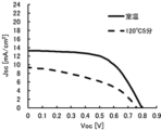
- FIG. 4 is a diagram showing JV curves obtained from Examples 3-3 and 3-4.
- FIG. 10 is a diagram showing JV curves obtained from Comparative Examples 3-1 and 3-2;
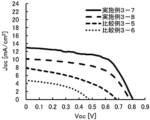
- FIG. 4 is a diagram showing JV curves obtained from Examples 3-7 and 3-8 and Comparative Examples 3-5 and 3-6.
- the charge-transporting composition of the present invention is a charge-transporting composition for forming a charge-transporting thin film in an organic photoelectric conversion device, and comprises a polythiophene derivative containing a repeating unit represented by the following formula (1). a charge-transporting substance and a solvent, wherein the electron-accepting dopant substance contains at least one selected from the group consisting of arylsulfonic acids and heteropolyacids represented by the following formula (2); The content of the organic solvent is 10% by mass or less.
- solid content is a general term for all components of the charge-transporting composition other than the solvent.
- R 1 and R 2 are each independently a hydrogen atom, an alkyl group having 1 to 40 carbon atoms, a fluoroalkyl group having 1 to 40 carbon atoms, an alkoxy group having 1 to 40 carbon atoms, or an alkoxy group having 1 to 40 carbon atoms.
- Y is an alkylene group having 1 to 40 carbon atoms substituted with a sulfonic acid group or a sulfonate group, which may contain an ether bond
- Z is a halogen atom is an alkylene group having 1 to 40 carbon atoms which may be substituted with p is an integer of 1 or more
- R e is a hydrogen atom, a sulfonic acid group or a carbon optionally substituted with a sulfonic acid group an alkyl group having 1 to 40 carbon atoms, a fluoroalkyl group having 1 to 40 carbon atoms optionally substituted with a sulfonic acid group or a sulfonic acid group,
- the alkyl group having 1 to 40 carbon atoms may be linear, branched or cyclic, and specific examples thereof include methyl, ethyl, n-propyl, isopropyl, n-butyl, isobutyl group, s-butyl group, t-butyl group, n-pentyl group, n-hexyl group, n-heptyl group, n-octyl group, n-nonyl group, n-decyl group, n-undecyl group, n- dodecyl group, n-tridecyl group, n-tetradecyl group, n-pentadecyl group, n-hexadecyl group, n-heptadecyl group, n-octadecyl group, n-nonadecyl group, n-eicosanyl group, behenyl group
- the fluoroalkyl group having 1 to 40 carbon atoms is not particularly limited as long as it is an alkyl group having 1 to 40 carbon atoms in which at least one hydrogen atom on the carbon atoms is substituted with a fluorine atom.
- the alkyl group therein may be linear, branched or cyclic. Specific examples thereof include methoxy, ethoxy, n-propoxy, i- propoxy group, c-propoxy group, n-butoxy group, i-butoxy group, s-butoxy group, t-butoxy group, n-pentoxy group, n-hexoxy group, n-heptyloxy group, n-octyloxy group, n-nonyloxy group, n-decyloxy group, n-undecyloxy group, n-dodecyloxy group, n-tridecyloxy group, n-tetradecyloxy group, n-pentadecyloxy group, n-hexadecyloxy group , n-heptadecyloxy group, n-octadecyloxy group, n-
- the fluoroalkoxy group having 1 to 40 carbon atoms is not particularly limited as long as it is an alkoxy group having 1 to 40 carbon atoms in which at least one hydrogen atom on the carbon atoms is substituted with a fluorine atom.
- fluoromethoxy group difluoromethoxy group, perfluoromethoxy group, 1-fluoroethoxy group, 2-fluoroethoxy group, 1,2-difluoroethoxy group, 1,1-difluoroethoxy group, 2,2-difluoroethoxy group, 1,1,2-trifluoroethoxy group, 1,2,2-trifluoroethoxy group, 2,2,2-trifluoroethoxy group, 1,1,2,2-tetrafluoroethoxy group, 1,2, 2,2-tetrafluoroethoxy group, perfluoroethoxy group, 1-fluoropropoxy group, 2-fluoropropoxy group, 3-fluoropropoxy group, 1,1-difluoropropoxy group, 1,2-difluoropropoxy group, 1, 3-difluoropropoxy group, 2,2-difluoropropoxy group, 2,3-difluoropropoxy group, 3,3-difluoropropoxy group, 1,1,2-
- the alkylene group having 1 to 40 carbon atoms may be linear, branched or cyclic, and specific examples include methylene, ethylene, propylene, trimethylene, tetramethylene, pentylene, Hexylene group, heptylene group, octylene group, nonylene group, decylene group, undecylene group, dodecylene group, tridecylene group, tetradecylene group, pentadecylene group, hexadecylene group, heptadecylene group, octadecylene group, nonadecylene group, eicosanylene group and the like.
- aryl group having 6 to 20 carbon atoms include a phenyl group, a tolyl group, a 1-naphthyl group, a 2-naphthyl group, a 1-anthryl group, a 2-anthryl group, a 9-anthryl group, a 1-phenanthryl group, 2-phenanthryl group, 3-phenanthryl group, 4-phenanthryl group, 9-phenanthryl group and the like, with phenyl group, tolyl group and naphthyl group being preferred.
- aryloxy group having 6 to 20 carbon atoms include phenoxy group, anthracenoxy group, naphthoxy group, phenanthreoxy group, fluorenoxy group and the like.
- Halogen atoms include fluorine, chlorine, bromine and iodine atoms.
- sulfonic acid groups and sulfonic acid groups include groups represented by the following formula (S).
- M represents a hydrogen atom, an alkali metal selected from the group consisting of Li, Na and K, NH(R S ) 3 or HNC 5 H 5 .
- R S independently represents a hydrogen atom, or represents an optionally substituted alkyl group having 1 to 6 carbon atoms.
- R S is an alkyl group having a substituent
- substituents include an alkyl group having 1 to 6 carbon atoms, an alkoxy group having 1 to 6 carbon atoms, an aryl group having 6 to 20 carbon atoms, and a hydroxy group. , an amino group, a carboxy group, and the like.
- alkyl group having 1 to 6 carbon atoms include the same groups as those exemplified for the above alkyl group.
- Specific examples of alkoxy groups having 1 to 6 carbon atoms include methoxy, ethoxy, n-propoxy, i-propoxy, n-butoxy, etc.
- aryl groups having 6 to 20 carbon atoms include phenyl, tolyl, 1-naphthyl, 2-naphthyl, 1-anthryl, 2-anthryl, 9-anthryl, 1-phenanthryl, 2-phenanthryl, 3-phenanthryl, 4-phenanthryl, 9-phenanthryl groups and the like.
- a hydroxy group is preferable as the substituent, and specific examples of the alkyl group having a hydroxy group include 2-hydroxyethyl group, 3-hydroxypropyl group, 2-hydroxypropyl group, 2,3-dihydroxypropyl group and the like. mentioned.
- R S is preferably a hydrogen atom or a linear or branched alkyl group having 1 to 3 carbon atoms, more preferably a hydrogen atom or a methyl group.
- R 1 and R 2 are each independently a hydrogen atom, a fluoroalkyl group having 1 to 40 carbon atoms, an alkoxy group having 1 to 40 carbon atoms, —O[C(R a R b )—C(R c R d )—O] p —R e , —OR f , a sulfonate group or a sulfonate group, or —O—Y— formed by combining R 1 and R 2 O- is preferred.
- R a to R d each independently represent a hydrogen atom, an alkyl group having 1 to 40 carbon atoms, a fluoroalkyl group having 1 to 40 carbon atoms, or an aryl group having 6 to 20 carbon atoms. Specific examples of these groups are the same as those listed above. Among them, R a to R d are each independently preferably a hydrogen atom, an alkyl group having 1 to 8 carbon atoms, a fluoroalkyl group having 1 to 8 carbon atoms, or a phenyl group.
- R e represents a hydrogen atom, an alkyl group having 1 to 40 carbon atoms, a fluoroalkyl group having 1 to 40 carbon atoms, or an aryl group having 6 to 20 carbon atoms. Specific examples of these groups are the same as those listed above. Among them, R e is preferably a hydrogen atom, an alkyl group having 1 to 8 carbon atoms, a fluoroalkyl group having 1 to 8 carbon atoms, or a phenyl group, and more preferably a hydrogen atom, a methyl group, a propyl group, or a butyl group. Also, p is preferably 1 to 5, more preferably 1, 2 or 3.
- R f is a hydrogen atom, an alkyl group having 1 to 40 carbon atoms, a fluoroalkyl group having 1 to 40 carbon atoms or an aryl group having 6 to 20 carbon atoms, but a hydrogen atom, an alkyl group having 1 to 8 carbon atoms, A fluoroalkyl group having 1 to 8 carbon atoms or a phenyl group is preferred, and -CH 2 CF 3 is more preferred.
- R 1 is preferably a hydrogen atom, a sulfonic acid group or a sulfonic acid group, more preferably a sulfonic acid group or a sulfonic acid group, and R 2 is preferably an alkoxy group having 1 to 40 carbon atoms.
- a group or -O-[Z-O] p -R e more preferably -O[C(R a R b )-C(R c R d )-O] p -R e or -OR f , more preferably preferably -O[C(R a R b )-C(R c R d )-O] p -R e , -O-CH 2 CH 2 -O-CH 2 CH 2 -O-CH 3 , -O -CH 2 CH 2 -O-CH 2 CH 2 -OH or -O-CH 2 CH 2 -OH, or -O-Y-O- formed by combining R 1 and R 2 together is.
- the polythiophene derivative according to a preferred embodiment of the present invention comprises a repeating unit in which R 1 is a sulfonic acid group or a sulfonate group and R 2 is other than a sulfonic acid group or a sulfonate group, or R 1 and R 2 are combined to form --O--Y--O--.
- R 1 is a sulfonic acid group or a sulfonic acid group
- R 2 is an alkoxy group having 1 to 40 carbon atoms or —O—[ZO] p —R e or repeat units wherein R 1 and R 2 are joined to form -O-Y-O-.
- R 1 is a sulfonic acid group or a sulfonic acid group
- R 2 is —O[C(R a R b )–C(R c R d )–O] p — It contains repeating units that are R e or —OR f .
- R 1 is a sulfonic acid group or a sulfonic acid group
- R 2 is —O[C(R a R b )–C(R c R d )–O] p It includes repeating units that are —R e or —O—Y—O— formed by combining R 1 and R 2 .
- R 1 is a sulfonic acid group or a sulfonic acid group
- R 2 is --O--CH 2 CH 2 --O--CH 2 CH 2 --O--CH 3 , --O-- CH 2 CH 2 —O—CH 2 CH 2 —OH or —O—CH 2 CH 2 —OH
- Y1 Includes repeat units that are represented groups.
- R y represents an alkyl group having 1 to 6 carbon atoms or a fluorine atom. M is the same as above.
- Examples of the alkyl group having 1 to 6 carbon atoms for R y include the same groups as exemplified in the description of R 1 and R 2 .
- An alkyl group having 1 to 3 carbon atoms is preferred, a methyl group and an ethyl group are more preferred, and a methyl group is even more preferred.
- polythiophene derivative examples include, for example, polythiophene containing at least one repeating unit represented by the following formulas (1-1) to (1-4).
- a polythiophene containing a repeating unit represented by the following formula (1-4) is more preferable because it is easily obtainable and has high solubility in a solvent.
- examples of suitable structures of the above polythiophene derivatives include polythiophene derivatives having a structure represented by the following formula (1a).
- each unit may be combined randomly or may be combined as a block polymer.
- M is the same as above.
- polythiophene derivatives may be homopolymers or copolymers (including statistical, random, gradient, and block copolymers).
- block copolymers include, for example, AB diblock copolymers, ABA triblock copolymers, and (AB) m -multiblock copolymers.
- Polythiophenes contain repeat units derived from other types of monomers such as thienothiophenes, selenophenes, pyrroles, furans, tellurophenes, anilines, arylamines, and arylenes such as phenylenes, phenylene vinylenes, and fluorenes. may contain.
- the content of the repeating unit represented by formula (1) in the polythiophene derivative is preferably more than 50 mol%, more preferably 80 mol% or more, more preferably 90 mol% of all repeating units contained in the polythiophene derivative.
- the above is more preferable, 95 mol % or more is more preferable, and 100 mol % is most preferable.
- the content of repeating units having a sulfonic acid group or a sulfonate group is 10% of the repeating units represented by formula (1) in the polythiophene derivative.
- mol % or more is preferred, 30 mol % or more is more preferred, 50 mol % or more is even more preferred, and 100 mol % is even more preferred.
- the polymer formed may contain repeating units derived from impurities, depending on the purity of the starting monomers used for polymerization.
- the term "homopolymer” means a polymer containing repeating units derived from one type of monomer, but may contain repeating units derived from impurities.
- the polythiophene derivative is preferably a polymer in which basically all the repeating units are the repeating units represented by the above formula (1). ) is more preferably a polymer containing at least one repeating unit.
- the polythiophene derivative contains a repeating unit having a sulfonic acid group
- at least part of the sulfonic acid group contained in the polythiophene derivative contains an amine compound from the viewpoint of further improving solubility and dispersibility in solvents.
- An added amine adduct is preferred.
- Amine compounds that can be used to form amine adducts include methylamine, ethylamine, n-propylamine, isopropylamine, n-butylamine, isobutylamine, s-butylamine, t-butylamine, n-pentylamine, n-hexylamine.
- n-heptylamine monoalkylamine compounds such as n-octylamine; aniline, primary amine compounds such as monoarylamine compounds such as tolylamine; N-ethylmethylamine, N-methyl-n-propylamine, N-methyl isopropylamine, N-methyl-n-butylamine, N-methyl-s-butylamine, N-methyl-t-butylamine, N-methylisobutylamine, diethylamine, N-ethyl-n-propylamine, N-ethylisopropylamine, N-ethyl-n-butylamine, N-ethyl-s-butylamine, N-ethyl-t-butylamine, dipropylamine, Nn-propylisopropylamine, Nn-propyl-n-butylamine, Nn- Bropyl-s-butylamine, aziridine (ethyleneimine), 2-
- secondary amine compounds such as alkylarylamine compounds such as diphenylamine and indoline; N,N-dimethylethylamine, N,N-dimethyl-n-propylamine, N,N-dimethylisopropylamine, N,N -dimethyl-n-butylamine, N,N-dimethyl-s-butylamine, N,N-dimethyl-t-butylamine, N,N-dimethylisobutylamine, N,N-diethylmethylamine, N-methyldi(n-propyl ) amine, N-methyldiisopropylamine, triethylamine, N,N-diethyl-n-butylamine, N,N-diisopropylethylamine, N,N-di(n-butyl)ethylamine, 1-methylacetidine, 1-methylpyrrolidine , 1-methylpiperidine and the like, but considering the balance between the solub
- the above polythiophene derivative or its amine adduct may be treated with a reducing agent.
- some of the repeating units constituting them may have an oxidized chemical structure called a "quinoid structure".
- the term "quinoid structure” is used for the term “benzenoid structure”, the latter being a structure containing an aromatic ring, whereas the former is a structure in which the double bond within the aromatic ring moves out of the ring (the As a result, the aromatic ring disappears), meaning a structure in which two exocyclic double bonds conjugated with other double bonds remaining in the ring are formed.
- R 1 and R 2 are as defined in formula (1) above.
- This quinoid structure is generated by a process in which the polythiophene derivative containing the repeating unit represented by the above formula (1) undergoes an oxidation reaction by a dopant, a so-called doping reaction, and imparts charge transport properties to the polythiophene derivative. It forms part of a structure called "bipolaron structure". These structures are known. Introduction of a "polaron structure” and/or a “bipolaron structure” is essential in the production of an organic solar cell element, and in fact, when producing an organic solar cell element, the thin film formed from the charge-transporting composition is baked. Sometimes the doping reactions described above are deliberately allowed to achieve this.
- the reason why the quinoid structure is included in the polythiophene derivative before the doping reaction is that the polythiophene derivative undergoes an unintended oxidation reaction equivalent to the doping reaction during the manufacturing process (especially the sulfonation step therein). This is thought to be due to the
- the polythiophene derivative when the polythiophene derivative is subjected to a reduction treatment using a reducing agent, even if the quinoid structure is excessively introduced into the polythiophene derivative, the quinoid structure is reduced by the reduction, and the solubility and dispersibility of the polythiophene derivative in an organic solvent are improved. is improved, it becomes possible to stably produce a good charge-transporting composition that gives a thin film with excellent uniformity.
- the conditions for the reduction treatment are such that the quinoid structure is reduced to appropriately convert to the non-oxidized structure, that is, the benzenoid structure (for example, in the polythiophene derivative containing the repeating unit represented by the above formula (1),
- the quinoid structure represented by the above formula (1′) is not particularly limited as long as it can be converted to the structure represented by the above formula (1), for example, in the presence of a suitable solvent or
- This treatment can be carried out simply by contacting the polythiophene derivative or amine adduct with a reducing agent in the absence thereof.
- a reducing agent is not particularly limited as long as the reduction is performed properly, but suitable examples include aqueous ammonia, hydrazine, etc., which are readily available on the market.
- the amount of the reducing agent varies depending on the amount of the reducing agent to be used, and cannot be categorically defined. It is 0.1 parts by mass or more and 10 parts by mass or less from the viewpoint of preventing excess reducing
- a polythiophene derivative or an amine adduct is stirred overnight at room temperature in 28% ammonia water.
- the reduction treatment under such relatively mild conditions sufficiently improves the solubility and dispersibility of the polythiophene derivatives and amine adducts in organic solvents.
- the reduction treatment may be performed before or after forming the amine adduct.
- the solubility and dispersibility of the polythiophene derivative or its amine adduct in the solvent change, and as a result, the polythiophene derivative or its amine adduct, which was not dissolved in the reaction system at the start of the treatment, will be removed after the treatment is completed. Sometimes dissolved. In such a case, an organic solvent (acetone, isopropyl alcohol, etc. in the case of sulfonated polythiophene) incompatible with the polythiophene derivative or its amine adduct is added to the reaction system to obtain the polythiophene derivative or its amine adduct.
- the polythiophene derivative or its amine adduct can be recovered by a method such as causing precipitation and filtering.
- Preferred specific examples of the quinoid structure of the above formula (1') include structures represented by the following formula (1'-1).
- the weight-average molecular weight of the polythiophene derivative containing the repeating unit represented by formula (1) or its amine adduct is preferably from about 1,000 to about 1,000,000, more preferably from about 5,000 to about 100,000. Preferably, from about 10,000 to about 50,000 is even more preferred.
- a weight average molecular weight is a polystyrene conversion value by a gel permeation chromatography.
- the polythiophene derivative or its amine adduct contained in the charge-transporting composition of the present invention may be only one kind of polythiophene derivative or its amine adduct containing a repeating unit represented by formula (1), or two kinds. or more.
- a commercially available product or a product obtained by polymerizing a thiophene derivative or the like as a starting material by a known method may be used. It is also preferable to use those purified by methods such as reprecipitation and ion exchange. By using the purified one, the characteristics of the organic solar cell element provided with the thin film obtained from the charge-transporting composition of the present invention can be further enhanced. Examples of commercially available products include SELFTRON (registered trademark) manufactured by Tosoh Corporation.
- conjugated polymers and sulfonated conjugated polymers are described in US Pat. No. 8,017,241 to Seshadri et al. Sulfonated polythiophenes are also described in WO2008/073149 and WO2016/171935.
- At least part of the polythiophene derivative containing the repeating unit represented by formula (1) or its amine adduct contained in the charge-transporting composition is dissolved in an organic solvent.
- a polythiophene derivative containing a repeating unit represented by formula (1) or an amine adduct thereof and a charge-transporting substance other than the polythiophene derivative containing the repeating unit may be used in combination.
- the ionization potential of the hole collection layer is preferably close to the ionization potential of the p-type semiconductor material in the active layer.
- the absolute value of the difference is preferably 0 to 1 eV, more preferably 0 to 0.5 eV, and even more preferably 0 to 0.2 eV. Therefore, the charge-transporting composition of the present invention contains an arylsulfonic acid compound represented by the following formula (2) and a heteropolyacid for the purpose of adjusting the ionization potential of the charge-transporting thin film obtained using the composition.
- A represents a naphthalene ring or anthracene ring
- B represents a divalent to tetravalent perfluorobiphenyl group
- l represents the number of sulfonic acid groups bonded to A, satisfying 1 ⁇ l ⁇ 4 is an integer
- q indicates the number of bonds between B and X, and is an integer satisfying 2 to 4.
- the arylsulfonic acid compound represented by formula (2) can be synthesized by a known method, for example, by the method described in International Publication No. 2006/025342.
- heteropoly acids include heteropolyacids such as phosphomolybdic acid, silicomolybdic acid, phosphotungstic acid, phosphotungstomolybdic acid, silicotungstic acid, sodium phosphomolybdate, and phosphovanadomolybdic acid described in WO 2010/058777.
- heteropolyacids such as phosphomolybdic acid, silicomolybdic acid, phosphotungstic acid, phosphotungstomolybdic acid, silicotungstic acid, sodium phosphomolybdate, and phosphovanadomolybdic acid described in WO 2010/058777.
- examples include inorganic oxidizing agents such as acid compounds.
- silicomolybdic acid and silicotungstic acid are preferred in consideration of solubility in solvents, particularly solubility in water.
- the content of the electron-accepting dopant substance is appropriately set in consideration of the type of the charge-transporting substance and the charge-transporting substance to be expressed. 0.05 to 10, preferably 0.1 to 3.0, more preferably 0.2 to 2.0.
- the mixing ratio of the arylsulfonic acid compound represented by the formula (2) and the heteropolyacid is 10:90 to 90:10 is preferred, and 20:80 to 80:20 is more preferred.
- the charge-transporting composition of the present invention may contain an electron-accepting dopant substance other than the arylsulfonic acid compound represented by formula (2) and the heteropolyacid.
- electron-accepting dopant substances include strong inorganic acids such as hydrogen chloride, sulfuric acid , nitric acid, phosphoric acid; boron chloride (BBr 3 ), boron trifluoride etherate (BF 3 OEt 2 ), iron chloride (III) (FeCl 3 ), copper chloride (II) (CuCl 2 ), antimony pentachloride (V) (SbCl 5 ), arsenic pentafluoride (V) (AsF 5 ), phosphorus pentafluoride (PF 5 ), tris(4-bromophenyl)aluminum hexachloroantimonate (TBPAH); Lewis acids such as benzenesulfonic acid, tosylic acid, hydroxyl Benzenes
- the content thereof is preferably 20% by mass or less, more preferably 10% by mass or less, and still more preferably not contained, based on the total electron-accepting dopant substances.
- the charge-transporting composition of the present invention may contain a surfactant.
- the surfactant is not particularly limited, and fluorine-based surfactants, acetylenic surfactants, alkyl-based surfactants, silicone-based surfactants, etc. can be used. It is preferred to use an active agent.
- the fluorosurfactant used in the present invention is available as a commercial product.
- Such commercial products include Capstone® FS-10, FS-22, FS-30, FS-31, FS-34, FS-35, FS-50, FS- 51, FS-60, FS-61, FS-63, FS-64, FS-65, FS-66, FS-81, FS-83, FS-3100; Daiichi Kogyo Seiyaku Co., Ltd. Neugen FN- 1287; Megafac F-444, F-477, F-559 manufactured by DIC Corporation, but not limited thereto.
- Capstone FS-30, 31, 34, 35 and 3100, Neugen FN-1287 and Megafac F-559, which are nonionic surfactants, are preferred.
- the fluorine-based surfactant is not particularly limited as long as it contains a fluorine atom, and may be cationic, anionic, or nonionic, but fluorine-based nonionic surfactants are preferred. At least one fluorine-based nonionic surfactant selected from the following formulas (A1) and (B1) is particularly preferred.
- R represents a monovalent organic group containing a fluorine atom
- n represents an integer of 1-20.
- organic groups include alkyl groups having 1 to 40 carbon atoms, aryl groups having 6 to 20 carbon atoms, aralkyl groups having 7 to 20 carbon atoms, and heteroaryl groups having 2 to 20 carbon atoms.
- aralkyl groups having 7 to 20 carbon atoms include benzyl group, p-methylphenylmethyl group, m-methylphenylmethyl group, o-ethylphenylmethyl group, m-ethylphenylmethyl group and p-ethylphenylmethyl. group, 2-propylphenylmethyl group, 4-isopropylphenylmethyl group, 4-isobutylphenylmethyl group, ⁇ -naphthylmethyl group and the like.
- heteroaryl groups include 2-thienyl, 3-thienyl, 2-furanyl, 3-furanyl, 2-oxazolyl, 4-oxazolyl, 5-oxazolyl, 3-isoxazolyl, 4 -isoxazolyl group, 5-isoxazolyl group, 2-thiazolyl group, 4-thiazolyl group, 5-thiazolyl group, 3-isothiazolyl group, 4-isothiazolyl group, 5-isothiazolyl group, 2-imidazolyl group, 4-imidazolyl group, 2 -pyridyl group, 3-pyridyl group, 4-pyridyl group, 2-pyrazyl group, 3-pyrazyl group, 5-pyrazyl group, 6-pyrazyl group, 2-pyrimidyl group, 4-pyrimidyl group, 5-pyrimidyl group, 6 -pyrimidyl group, 3-pyridazyl group, 4-pyridazyl group, 5-pyridazyl group
- n is not particularly limited as long as it is an integer of 1-20, but an integer of 1-10 is more preferable.
- n has the same meaning as above.
- a specific example of the perfluoroalkyl group having 1 to 40 carbon atoms is a group in which all the hydrogen atoms of the alkyl group having 1 to 40 carbon atoms are substituted with fluorine atoms.
- acetylenic surfactant a commercially available product can also be used, and specific examples include Surfynol-104, Surfynol-420, Surfynol-440, Surfynol-465, Surfynol-485, Dynol-604, etc. manufactured by Evonik. Examples include, but are not limited to.
- alkyl-based surfactants Commercially available products can also be used as alkyl-based surfactants, and specific examples include Pluronic-10R5, Pluronic-25R5, Pluronic F-127, Pluronic-L44, Genapol X-080 and Genapol manufactured by Sigma-Aldrich. Examples include, but are not limited to, X-100, Genapol C-100, and lgepal C0-430 and lgepal CA-630 manufactured by Solvay.
- a surfactant When a surfactant is included, its content is not particularly limited. About 0.01 to 0.1% by mass of the whole is preferable, 0.02 to 0.08% by mass is more preferable, and 0.03 to 0.06% by mass is most preferable.
- compositions of the present invention may contain one or more metal oxide nanoparticles.
- a nanoparticle means a fine particle having an average primary particle size of the order of nanometers (typically 500 nm or less).
- Metal oxide nanoparticles refer to metal oxides shaped into nanoparticles.
- a nanoparticle means a fine particle having an average primary particle size of the order of nanometers (typically 500 nm or less).
- Metal oxide nanoparticles refer to metal oxides shaped into nanoparticles.
- the primary particle size of the metal oxide nanoparticles used in the present invention is not particularly limited as long as it is nano-sized. 100 nm is more preferred, and 5 to 50 nm is even more preferred.
- the particle size is a measured value using a nitrogen adsorption isotherm by the BET method.
- Metals constituting metal oxide nanoparticles in the present invention include not only metals in the usual sense, but also semimetals.
- Metals in the usual sense include, but are not limited to, tin (Sn), titanium (Ti), aluminum (Al), zirconium (Zr), zinc (Zn), niobium (Nb), tantalum ( It is preferable to use one or more selected from the group consisting of Ta) and W (tungsten).
- metalloids refer to elements whose chemical and/or physical properties are intermediate between those of metals and nonmetals. A universal definition of metalloids has not been established, but in the present invention, a total of six Let the elements be semimetals. These semimetals may be used alone or in combination of two or more, and may also be used in combination with metals in the usual sense.
- Metal oxide nanoparticles used in the present invention include boron (B), silicon (Si), germanium (Ge), arsenic (As), antimony (Sb), tellurium (Te), tin (Sn), titanium (Ti) , aluminum (Al), zirconium (Zr), zinc (Zn), niobium (Nb), tantalum (Ta) and W (tungsten).
- the metal oxide may be a mixture of oxides of individual single metals, or a composite oxide containing a plurality of metals.
- metal oxides include B2O3 , B2O, SiO2 , SiO, GeO2 , GeO, As2O4 , As2O3 , As2O5 , Sb2O3 , Sb2 . O5 , TeO2 , SnO2 , ZrO2 , Al2O3 , ZnO and the like, but also B2O3 , B2O , SiO2 , SiO , GeO2 , GeO, As2O4 , As2 . O3 , As2O5 , SnO2 , SnO, Sb2O3 , TeO2 , and mixtures thereof are preferred , with SiO2 being more preferred.
- the metal oxide nanoparticles may contain one or more organic capping groups.
- This organic capping group may be reactive or non-reactive.
- Examples of reactive organic capping groups include organic capping groups that can be crosslinked by UV light or radical initiators.
- silica sol in which SiO 2 nanoparticles are dispersed in a dispersion medium as the metal oxide nanoparticles.
- the silica sol is not particularly limited, and can be appropriately selected from known silica sols and used. Commercially available silica sols are usually in the form of dispersions.
- SiO2 nanoparticles are mixed with various solvents such as water, methanol, methyl ethyl ketone, methyl isobutyl ketone, N,N-dimethylacetamide, ethylene glycol, isopropanol, methanol, ethylene glycol monopropyl ether, cyclohexanone, acetic acid.
- solvents such as water, methanol, methyl ethyl ketone, methyl isobutyl ketone, N,N-dimethylacetamide, ethylene glycol, isopropanol, methanol, ethylene glycol monopropyl ether, cyclohexanone, acetic acid.
- solvent water-soluble alcohols are preferable, and methanol, 2-propanol and ethylene glycol are more preferable.
- silica sols include Snowtex (registered trademark) ST-O, ST-OS, ST-O-40 and ST-OL manufactured by Nissan Chemical Industries, Ltd., and Silidol 20 manufactured by Nippon Chemical Industries Co., Ltd. , 30, 40, etc.; methanol silica sol manufactured by Nissan Chemical Co., Ltd., MA-ST-M, MA-ST-L, IPA-ST, IPA-ST-L, IPA-ST-ZL, EG- Examples include, but are not limited to, organosilica sols such as ST.
- the solid content concentration of the silica sol is also not particularly limited, but is preferably 5 to 60% by mass, more preferably 10 to 50% by mass, and even more preferably 15 to 30% by mass.
- the content is not particularly limited, but in consideration of sufficient adhesion to the active layer, 50 parts per 100 parts by mass of the charge-transporting substance. ⁇ 95 parts by mass is preferable, 60 to 95 parts by mass is more preferable, and 80 to 95 parts by mass is even more preferable.
- the charge-transporting substance is used as a solution or dispersion, the amount of metal oxide nanoparticles to be added is based on the solid content of the charge-transporting substance.
- the composition of the present invention may contain an alkoxysilane.
- alkoxysilane By containing alkoxysilane, it is possible to improve the solvent resistance and water resistance of the obtained thin film, improve the electron blocking property, and optimize the HOMO level and LUMO level for the active layer.
- the alkoxysilane may be a siloxane-based material.
- any one or more alkoxysilanes selected from tetraalkoxysilane, trialkoxysilane and dialkoxysilane can be used.
- Methoxysilane, methyltriethoxysilane, methyltrimethoxysilane, 3,3,3-trifluoropropyltrimethoxysilane, dimethyldiethoxysilane and dimethyldimethoxysilane are preferred, and tetraethoxysilane is more preferred.
- siloxane-based materials include polysiloxanes such as poly(tetraethoxysilane) and poly(phenylethoxysilane) obtained by reactions such as hydrolysis of the alkoxysilanes.
- alkoxysilane When alkoxysilane is used, its content is not particularly limited as long as it exhibits the above effects. 0.01 to 50 times is more preferred, and 0.05 to 10 times is even more preferred.
- the charge-transporting composition of the present invention may further contain a matrix polymer, if necessary.
- a matrix polymer include matrix polymers containing repeating units represented by the following formula (I) and repeating units represented by the following formula (II).
- R 3 , R 4 , R 5 , R 6 , R 7 , R 8 and R 9 are each independently a hydrogen atom, a halogen atom, a fluoroalkyl group having 1 to 20 carbon atoms, or a a perfluoroalkyl group of 1 to 20,
- Q is -[OC(R h R i )-C(R j R k )] y -O-[CR l R m ] z -SO 3 H
- R h , R i , R j , R k , R l and R m are each independently a hydrogen atom, a halogen atom, a C 1-20 fluoroalkyl group, or a C 1-20 perfluoroalkyl group, y is 0-10, and z is 1-5.
- halogen atom the fluoroalkyl group having 1 to 20 carbon atoms
- perfluoroalkyl group having 1 to 20 carbon atoms are the same as those described above.
- R 3 , R 4 , R 5 and R 6 are preferably a fluorine atom or a chlorine atom, R 3 , R 5 and R 6 are a fluorine atom and R 4 is a chlorine atom is more preferred, and it is even more preferred that all of R 3 , R 4 , R 5 and R 6 are fluorine atoms.
- R 7 , R 8 and R 9 are preferably fluorine atoms.
- R h , R i , R j , R k , R l and R m are preferably a fluorine atom, a C 1-8 fluoroalkyl group, or a C 1-8 perfluoroalkyl group.
- R l and R m are fluorine atoms.
- y is preferably 0, and z is preferably 2.
- R 3 , R 5 and R 6 above are a fluorine atom
- R 4 is a chlorine atom
- each of R 1 and R m is a fluorine atom
- y is 0
- z is preferably two.
- each R3 , R4 , R5 , and R6 is a fluorine atom; and each R1 and Rm is a fluorine atom; y is 0; and z is preferably two.
- the ratio (s:t ratio) between the number "s" of repeating units represented by formula (I) and the number "t” of repeating units represented by formula (II) is not particularly limited.
- the s:t ratio is preferably 9:1 to 1:9, more preferably 8:2 to 2:8.
- the matrix polymer that can be suitably used in the present invention may be synthesized using a known method or may be a commercially available product.
- the polymer containing the repeating unit represented by the formula (I) and the repeating unit represented by the formula (II) is represented by the monomer represented by the following formula (Ia) and the following formula (IIa)
- Monomers can be prepared by copolymerization by known polymerization methods, followed by hydrolysis of the sulfonyl fluoride groups to convert them to sulfonic acid groups.
- TFE tetrafluoroethylene
- CFE chlorotrifluoroethylene
- F 2C CF-[O- CF2 - CR12FO ] y - CF2 - CF2 - SO2F where R12 is F or CF3 and y is 1 to 10
- F 2 C CF-O-CF 2 -CF 2 -CF 2 -SO 2 F
- F 2 C CF-OCF 2 -CF 2 -CF 2 -CF 2 -SO 2 F, etc.
- the matrix polymer means the mass (g/mol) of the matrix polymer per 1 mol of acid groups present in the matrix polymer.
- the equivalent weight of the matrix polymer is preferably from about 400 to about 15,000 g/mol, more preferably from about 500 to about 10,000 g/mol, even more preferably from about 500 to about 8,000 g/mol, even more preferably about 500 to about 2,000 g/mol, most preferably about 600 to about 1,700 g/mol.
- Such matrix polymers are commercially available.
- Commercially available products include, for example, NAFION (registered trademark) manufactured by DuPont, AQUIVION (registered trademark) manufactured by Solvay Specialty Polymers, and FLEMION (registered trademark) manufactured by Asahi Glass Co., Ltd., and the like.
- the matrix polymer is preferably polyethersulfone containing at least one repeating unit containing at least one sulfonic acid residue (--SO 3 H).
- composition of the present invention may contain other additives as long as the object of the present invention can be achieved.
- the type of additive can be appropriately selected from known additives depending on the desired effect.
- a highly soluble solvent that can dissolve the polythiophene derivative and the electron-accepting dopant substance well can be used as the solvent for preparing the charge-transporting composition.
- the highly soluble solvent can be used alone or in combination of two or more, and the amount used can be 5 to 100% by mass of the total solvent used in the composition.
- solvents examples include water; alcohol solvents such as ethanol, 2-propanol, 1-butanol, 2-butanol, s-butanol, t-butanol, 1-methoxy-2-propanol; - amides such as methylformamide, N,N-dimethylformamide, N,N-diethylformamide, N-methylacetamide, N,N-dimethylacetamide, N-methylpyrrolidone, 1,3-dimethyl-2-imidazolidinone
- Organic solvents such as solvents can be mentioned.
- at least one solvent selected from water and alcoholic solvents is preferred, water, ethanol and 2-propanol are more preferred, water and 2-propanol are still more preferred, and water is even more preferred.
- the above highly soluble solvents can be used alone or in combination of two or more.
- the content of the organic solvent in the solvent is 10% by mass or less, preferably 5% by mass or less. (that is, the solvent is only water) is more preferable.
- both the charge-transporting substance and the electron-accepting dopant substance are completely dissolved in the solvent or are in a state of being uniformly dispersed. Considering obtaining a pore-collecting layer with good reproducibility, it is more preferable that these substances are completely dissolved in the solvent.
- the charge-transporting composition of the present invention has a viscosity of 10 to 200 mPa ⁇ s, particularly 35 to 150 mPa ⁇ s at 25° C. in order to improve film-forming properties and ejection properties from a coating apparatus.
- the high-viscosity organic solvent is not particularly limited, and examples include cyclohexanol, ethylene glycol, 1,3-octylene glycol, diethylene glycol, dipropylene glycol, triethylene glycol, tripropylene glycol, and 1,3-butane. diol, 2,3-butanediol, 1,4-butanediol, propylene glycol, hexylene glycol and the like.
- the addition ratio is preferably within a range in which solids do not precipitate, and as long as solids do not precipitate, the total content of the organic solvent exemplified in the above highly soluble solvent , preferably 10% by mass or less in the solvent, more preferably 5% by mass or less, and more preferably not contained (0% by mass).
- solvents examples include butyl cellosolve, diethylene glycol diethyl ether, diethylene glycol dimethyl ether, diethylene glycol monoethyl ether acetate, diethylene glycol monobutyl ether acetate, dipropylene glycol monomethyl ether, propylene glycol monomethyl ether, propylene glycol monomethyl ether acetate, ethyl carbitol, diacetone alcohol, ⁇ -butyrolactone, ethyl lactate, n-hexyl acetate and the like.
- the addition ratio is preferably 1 to 90% by mass, more preferably 1 to 50% by mass, of the total solvent used in the composition.
- the solid content concentration of the composition of the present invention is appropriately set in consideration of the viscosity and surface tension of the composition, the thickness of the thin film to be produced, etc., but is usually 0.1 to 10.0 mass. %, preferably 0.5 to 5.0% by mass, more preferably 1.0 to 3.0% by mass.
- the viscosity of the charge-transporting composition used in the present invention may be appropriately adjusted depending on the coating method, taking into consideration the thickness of the thin film to be produced and the solid content concentration. ⁇ 50 mPa ⁇ s.
- a charge-transporting substance, a surfactant, a metal oxide nanoparticle, an electron-accepting dopant substance, a solvent, and the like are used as long as the solid content is uniformly dissolved or dispersed in the solvent. They can be mixed in any order.
- a method of dissolving a polythiophene derivative in a solvent and then dissolving an electron-accepting dopant substance in the solution a method of dissolving an electron-accepting dopant substance in a solvent and then dissolving a polythiophene derivative in the solution
- Any method of mixing a polythiophene derivative and an electron-accepting dopant substance and then dissolving the mixture in a solvent can be employed as long as the solid content is uniformly dissolved or dispersed in the solvent.
- the order of adding the matrix polymer and the alkoxysilane is also arbitrary.
- the preparation of the composition is carried out under an inert gas atmosphere at normal temperature and normal pressure. bottom) or while heating.
- the composition described above is coated on the anode in the case of a forward stacking type organic thin film solar cell, or on the active layer in the case of a reverse stacking type organic thin film solar cell, and then sintered to obtain the hole collection of the present invention. It can form layers.
- the viscosity and surface tension of the composition, the thickness of the desired thin film, etc. are taken into consideration, and the drop casting method, spin coating method, blade coating method, dip coating method, roll coating method, bar coating method, die coating method, An optimum wet process method such as an inkjet method, a printing method (letterpress, intaglio, lithography, screen printing, etc.) may be adopted. Further, coating is usually carried out in an inert gas atmosphere at normal temperature and pressure. You may carry out, and you may carry out while heating.
- the film thickness is not particularly limited, it is preferably about 0.1 to 800 nm, more preferably about 30 to 500 nm in any case.
- a method for changing the film thickness there are methods such as changing the solid content concentration in the composition and changing the amount of the solution at the time of coating.
- a method for producing an organic thin-film solar cell using the charge-transporting composition of the present invention as a composition for forming a hole-collecting layer will be described below, but the present invention is not limited thereto.
- Laminated organic thin film solar cell A process of forming a layer of anode material on the surface of a transparent substrate to manufacture a transparent electrode.
- Inorganic oxides such as zinc oxide (IZO), metals such as gold, silver and aluminum, and highly charge-transporting organic compounds such as polythiophene derivatives and polyaniline derivatives can be used. Among these, ITO is most preferred.
- the transparent substrate a substrate made of glass or transparent resin can be used as the transparent substrate. The method for forming the anode material layer (anode layer) is appropriately selected according to the properties of the anode material.
- a dry process such as a vacuum deposition method or a sputtering method is selected. Considering the thickness of the thin film, etc., the optimum one is adopted from among the various wet process methods described above.
- a commercially available transparent anode substrate can also be used, and in this case, from the viewpoint of improving the yield of the device, it is preferable to use a substrate that has been smoothed.
- the method for producing an organic thin film solar cell of the present invention does not include the step of forming an anode layer.
- an inorganic oxide such as ITO
- surface treatment such as UV ozone treatment and oxygen-plasma treatment immediately before use.
- the anode material is mainly composed of an organic substance, surface treatment may not be performed.
- a step of forming an active layer on the formed hole collection layer It may be a laminate of layers or a non-laminate thin film made of a mixture of these materials.
- the active layer may be either an FA active layer or an NFA active layer, and any combination can significantly improve the durability of the resulting device.
- the deep Ip of the resulting charge-transporting thin film can reduce the energy gap with the NFA active layer, enabling the device to operate at a higher voltage.
- the NFA active layer means an active layer in which the content of NFA is 70% by mass or more in the n-type semiconductor contained in the active layer in the present invention.
- the FA active layer means an active layer in which the content of FA is 70 mass % or more of the n-type semiconductor contained in the active layer.
- n-type semiconductor materials used for the FA active layer include fullerene, [6,6]-phenyl-C 61 -butyric acid methyl ester (PC 61 BM), [6,6]-phenyl-C 71 -butyric acid methyl ester ( PC 71 BM) and the like.
- n-type semiconductor material used for the NFA active layer examples include compounds represented by the following formulas (3-1) to (3-4).
- Examples of the p-type semiconductor material that can be combined with the n-type semiconductor material include regioregular poly(3-hexylthiophene) (P3HT), PTB7 represented by the following formula (4-1), and the following formula (4-2).
- P3HT regioregular poly(3-hexylthiophene)
- PTB7 represented by the following formula (4-1)
- 4-2 regioregular poly(3-hexylthiophene)
- 4-1 regioregular poly(3-hexylthiophene)
- 4-1 regioregular poly(3-hexylthiophene)
- 4-1 regioregular poly(3-hexylthiophene)
- 4-1 regioregular poly(3-hexylthiophene)
- 4-1 regioregular poly(3-hexylthiophene)
- 4-1 regioregular poly(3-he
- n-type semiconductor material compounds represented by formulas (3-1) and (3-2) are preferable, and among them, BTP-4F in which X is F is more preferable in the former, and BTP-4F in which X is F in the latter ITIC-4F in which both X 1 and X 2 are F is more preferred.
- the p-type semiconductor material polymers containing a thiophene skeleton in the main chain, such as PM6 and PTB7, are preferable.
- thiophene skeleton in the main chain refers to a divalent aromatic ring consisting only of thiophene, or thienothiophene, benzothiophene, dibenzothiophene, benzodithiophene, naphthothiophene, naphthodithiophene, anthrathiophene, anthradithiophene.
- alkyl group having 1 to 20 carbon atoms alkenyl group having 2 to 20 carbon atoms, alkynyl group having 2 to 20 carbon atoms, haloalkyl group having 1 to 20 carbon atoms, aryl group having 6 to 20 carbon atoms, carbon It may be substituted with an aralkyl group having 7 to 20 carbon atoms or an acyl group having 1 to 20 carbon atoms.
- the halogen atom, the alkyl group having 1 to 20 carbon atoms, the alkoxy group having 1 to 20 carbon atoms, the aryl group having 6 to 20 carbon atoms, and the aralkyl group having 7 to 20 carbon atoms are the same as those exemplified above. are mentioned.
- thioalkoxy group having 1 to 20 carbon atoms include groups obtained by substituting the oxygen atom of the above alkoxy group with a sulfur atom.
- thioalkoxy (alkylthio) groups having 1 to 20 carbon atoms include methylthio, ethylthio, n-propylthio, isopropylthio, n-butylthio, isobutylthio, s-butylthio and t-butylthio.
- n-pentylthio group n-hexylthio group, n-heptylthio group, n-octylthio group, n-nonylthio group, n-decylthio group, n-undecylthio group, n-dodecylthio group, n-tridecylthio group, n-tetra decylthio group, n-pentadecylthio group, n-hexadecylthio group, n-heptadecylthio group, n-octadecylthio group, n-nonadecylthio group, n-eicosanylthio group and the like.
- alkenyl groups having 2 to 20 carbon atoms include ethenyl group, n-1-propenyl group, n-2-propenyl group, 1-methylethenyl group, n-1-butenyl group, n-2-butenyl group, n-3-butenyl group, 2-methyl-1-propenyl group, 2-methyl-2-propenyl group, 1-ethylethenyl group, 1-methyl-1-propenyl group, 1-methyl-2-propenyl group, n- 1-pentenyl group, n-1-decenyl group, n-1-eicosenyl group and the like.
- alkynyl groups having 2 to 20 carbon atoms include ethynyl, n-1-propynyl, n-2-propynyl, n-1-butynyl, n-2-butynyl and n-3-butynyl.
- haloalkyl groups having 1 to 20 carbon atoms include groups obtained by substituting at least one hydrogen atom in the above alkyl group with a halogen atom.
- Halogen atoms may be chlorine, bromine, iodine or fluorine atoms. Among them, a fluoroalkyl group is preferred, and a perfluoroalkyl group is more preferred.
- Specific examples thereof include a fluoromethyl group, a difluoromethyl group, a trifluoromethyl group, a pentafluoroethyl group, a 2,2,2-trifluoroethyl group, a heptafluoropropyl group, a 2,2,3,3,3- pentafluoropropyl group, 2,2,3,3-tetrafluoropropyl group, 2,2,2-trifluoro-1-(trifluoromethyl)ethyl group, nonafluorobutyl group, 4,4,4-trifluoro butyl group, undecafluoropentyl group, 2,2,3,3,4,4,5,5,5-nonafluoropentyl group, 2,2,3,3,4,4,5,5-octafluoro pentyl group, tridecafluorohexyl group, 2,2,3,3,4,4,5,5,6,6,6-undecafluorohexyl group, 2,2,3,3,4,4,5 , 5,6,6-
- acyl groups having 1 to 20 carbon atoms include formyl group, acetyl group, propionyl group, butyryl group, isobutyryl group, valeryl group, isovaleryl group, benzoyl group and the like.
- n-type semiconductor material contained in the active layer contains the n-type semiconductor material corresponding to the above NFA as the balance.
- n-type semiconductor materials include BTP-4F and ITIC-4F.
- the n-type semiconductor material corresponding to the above-mentioned FA is used as the balance in the range of less than 30% by mass of the n-type semiconductor material contained in the active layer. may be included.
- the same dry process as described above is selected when the active layer material is a poorly soluble sublimable material, and when it is a solution material or a dispersion liquid material, Considering the viscosity and surface tension of the composition, the desired thickness of the thin film, and the like, the most suitable one is adopted from among the various wet process methods described above.
- An electron collecting layer may be formed.
- Materials for forming the electron collection layer include lithium oxide (Li 2 O), magnesium oxide (MgO), alumina (Al 2 O 3 ), lithium fluoride (LiF), sodium fluoride (NaF), and magnesium fluoride.
- the various dry processes described above are selected. Considering the viscosity, surface tension, desired thickness of the thin film, etc., the optimum wet process method is adopted from among the various wet process methods described above.
- a step of forming a cathode layer on the formed electron collection layer metals such as barium, silver, and gold; inorganic oxides such as indium tin oxide (ITO) and indium zinc oxide (IZO); and highly charge-transporting organic compounds such as polythiophene derivatives and polyaniline derivatives. can be used by laminating or mixing the cathode materials.
- metals such as barium, silver, and gold
- inorganic oxides such as indium tin oxide (ITO) and indium zinc oxide (IZO)
- highly charge-transporting organic compounds such as polythiophene derivatives and polyaniline derivatives.
- the various dry processes described above are selected. Considering the viscosity and surface tension of the film, the desired thickness of the thin film, etc., the optimum one is adopted from among the various wet process methods described above.
- a carrier block layer may be provided between arbitrary layers for the purpose of controlling the rectification of photocurrent.
- a carrier blocking layer When a carrier blocking layer is provided, an electron blocking layer is usually inserted between the active layer and the hole collecting layer or the anode, and a hole blocking layer is inserted between the active layer and the electron collecting layer or the cathode.
- Materials for forming the hole blocking layer include titanium oxide, zinc oxide, tin oxide, bathocuproine (BCP), 4,7-diphenyl-1,10-phenanthroline (BPhen), and the like.
- Materials for forming the electron blocking layer include N,N'-di(1-naphthyl)-N,N'-diphenylbenzidine ( ⁇ -NPD) and triarylamine-based materials such as poly(triarylamine) (PTAA). materials and the like.
- the various dry processes described above are selected. Considering the viscosity and surface tension of the composition, the desired thickness of the thin film, and the like, the most suitable one is adopted from among the various wet process methods described above.
- the dry process described above is selected in the case of the poorly soluble and difficultly dispersible sublimable material, and in the case of the solution material or dispersion liquid material, the viscosity of the composition and the Considering the surface tension, the desired thickness of the thin film, etc., the most suitable wet process method is adopted from among the various wet process methods described above.
- a commercially available transparent cathode substrate can be suitably used, and from the viewpoint of improving the yield of the device, it is preferable to use a substrate that has been smoothed.
- the method for producing an organic thin-film solar cell of the present invention does not include the step of forming a cathode layer.
- an inorganic oxide is used as a cathode material to form a transparent cathode substrate, it may be subjected to the same cleaning treatment and surface treatment as those for the sequentially laminated anode material.
- a trapping layer may be formed.
- Materials for forming the electron collection layer include zinc oxide (ZnO), titanium oxide (TiO), tin oxide (SnO), etc., in addition to the materials exemplified in the above-mentioned forward stacking type materials.
- the above-described dry process is selected in the case of a poorly soluble or difficultly dispersible sublimation material, and in the case of a solution material or a dispersion liquid material, the viscosity and surface tension of the composition are adjusted to the desired value.
- the optimum one is adopted from among the various wet process methods described above.
- a method of forming an inorganic oxide precursor layer on the cathode using a wet process (particularly spin coating or slit coating) and firing to form an inorganic oxide layer can also be employed.
- the active layer consists of an n-layer, which is a thin film made of an n-type semiconductor material, and a p-layer, which is a thin film made of a p-type semiconductor material. or a non-laminated thin film made of a mixture of these materials.
- the n-type and p-type semiconductor materials include the same materials as those exemplified in the above-mentioned forward stacking type semiconductor materials. are preferably polymers containing a thiophene skeleton in the main chain, such as PM6 and PTB7.
- the method for forming the active layer is also the same as the method described for the forward lamination type active layer.
- a step of forming an anode layer on the formed hole collection layer. is the same as that of the positively laminated cathode layer.
- a carrier block layer may be provided between arbitrary layers for the purpose of controlling the rectification of photocurrent.
- Materials for forming the hole blocking layer and materials for forming the electron blocking layer are the same as those described above, and the method for forming the carrier blocking layer is also the same as described above.
- the OPV element manufactured by the method exemplified above is introduced into the glove box again and sealed in an inert gas atmosphere such as nitrogen. It is possible to exhibit the function as a solar cell and to measure the solar cell characteristics.
- a sealing method a concave glass substrate having a UV curable resin attached to the edge is attached to the film forming surface side of the organic thin film solar cell element in an inert gas atmosphere, and the resin is cured by UV irradiation.
- a film-sealing type sealing method using a method such as sputtering under vacuum is a method such as sputtering under vacuum.
- D1 manufactured by Fuji Film Wako Pure Chemical Industries, Ltd.
- D1 Fuji Film Wako Pure Chemical Industries, Ltd.
- D1 was added to prepare a dark blue solution with a concentration of 0.65% by mass.
- the resulting dark blue solution was filtered through a syringe filter with a pore size of 0.45 ⁇ m to obtain a hole-collecting layer composition A1.
- Example 1-2 To a solution of 1.25 g of P1 added with 3.73 g of pure water, 5.00 mg of S1, and 1.00 mg of S2, silicotungstic acid n-hydrate (manufactured by Alfa Aesar Co., Ltd.) (hereinafter: D2) was added. 7.50 mg was added to prepare a dark blue solution with a concentration of 0.65% by mass. The resulting dark blue solution was filtered through a syringe filter with a pore size of 0.45 ⁇ m to obtain a hole-collecting layer composition A2.
- D2 silicotungstic acid n-hydrate
- Example 1-3 7.50 mg of D1 to a solution of 1.25 g of P1, 3.71 g of pure water, 5.00 mg of S1, and 1.00 mg of S2, synthesized based on the description of WO 2006/025342 25.0 mg of the arylsulfonic acid compound A (hereinafter referred to as D3) represented by formula (2-1) was added to prepare a dark blue solution having a concentration of 1.15% by mass. The resulting dark blue solution was filtered through a syringe filter with a pore size of 0.45 ⁇ m to obtain a hole-collecting layer composition A3.
- D3 arylsulfonic acid compound A
- Example 1-4 7.50 mg of D2 and 25.0 mg of D3 were added to a solution in which 3.71 g of pure water, 5.00 mg of S1 and 1.00 mg of S2 were added to 1.25 g of P1 to obtain a concentration of 1.15% by mass. A blue solution was prepared. The resulting dark blue solution was filtered through a syringe filter with a pore size of 0.45 ⁇ m to obtain a hole-collecting layer composition A4.
- Example 1-5 3.21 g of pure water, 0.49 g of isopropanol, 5.00 mg of S1, and 1.00 mg of S2 were added to 1.25 g of P1. A 0.15% by weight dark blue solution was prepared. The resulting dark blue solution was filtered through a syringe filter with a pore size of 0.45 ⁇ m to obtain a hole-collecting layer composition A5.
- Example 1-6 12 molybdo (IV) phosphate n-hydrate (manufactured by Fujifilm Wako Pure Chemical Industries, Ltd.) ) (hereinafter: D4) was added to prepare a dark blue solution having a concentration of 0.65% by mass. The resulting dark blue solution was filtered through a syringe filter with a pore size of 0.45 ⁇ m to obtain a hole-collecting layer composition A6.
- Example 1-7 12 Tungsto (IV) phosphate n-hydrate (manufactured by Fujifilm Wako Pure Chemical Industries, Ltd.) ) (hereinafter referred to as D5) was added to prepare a dark blue solution having a concentration of 0.65% by mass. The resulting dark blue solution was filtered through a syringe filter with a pore size of 0.45 ⁇ m to obtain a hole-collecting layer composition A7.
- Table 1 summarizes the ink compositions of Examples 1-1 to 1-7.
- Table 2 summarizes the ink compositions of Comparative Examples 1-1 to 1-9.
- the film thickness of the active layer was about 100 nm.
- the hole-collecting layer composition A1 prepared in Example 1-1 was applied onto the active layer by a blade coating method to form a hole-collecting layer.
- the film thickness of the hole collection layer was about 100 nm.
- the laminated substrate is placed in a vacuum deposition apparatus, the apparatus is evacuated to a degree of vacuum of 1 ⁇ 10 ⁇ 3 Pa or less, and a silver layer serving as an anode is formed to a thickness of 100 nm by resistance heating.
- a reverse lamination type OPV element having an area of 10 mm ⁇ 10 mm at the intersection of the striped ITO layer and the silver layer was fabricated.
- Example 3-2 After applying the hole-collecting layer composition A1 by a blade coating method, an inverse lamination type OPV element was formed in the same manner as in Example 3-1, except that annealing was performed on a hot plate at 120 ° C. for 5 minutes. was made.
- Example 3-3 A reverse laminated OPV element was fabricated in the same manner as in Example 3-1, except that the hole-collecting layer composition A3 was used instead of the hole-collecting layer composition A1.
- Example 3-4 A reverse laminated OPV element was produced in the same manner as in Example 3-2, except that the hole-collecting layer composition A3 was used instead of the hole-collecting layer composition A1.
- Example 3-5 A reverse laminated OPV element was produced in the same manner as in Example 3-1, except that the hole-collecting layer composition A4 was used instead of the hole-collecting layer composition A1.
- Example 3-6 A reverse laminated OPV element was fabricated in the same manner as in Example 3-2, except that the hole-collecting layer composition A4 was used instead of the hole-collecting layer composition A1.
- Example 3-7 A reverse stacked OPV device was fabricated in the same manner as in Example 3-4, except that the thickness of the hole collection layer was about 300 nm.
- Example 3-8 A reverse laminated OPV element was fabricated in the same manner as in Example 3-7, except that the hole-collecting layer composition A5 was used instead of the hole-collecting layer composition A3.
- Example 3-9 A reverse lamination type OPV element was fabricated in the same manner as in Example 3-1 except that the FA active layer PV-F1062 (manufactured by Merck) was used instead of the NFA active layer PV-X Plus (manufactured by Raynergy tek). .
- Example 3-10 A reverse lamination type OPV element was fabricated in the same manner as in Example 3-5, except that the FA active layer PV-F1062 (manufactured by Merck & Co.) was used instead of the NFA active layer PV-X Plus (manufactured by Raynergy tek).
- Example 3-1 A reverse laminated OPV element was fabricated in the same manner as in Example 3-1, except that the hole-collecting layer composition B3 was used instead of the hole-collecting layer composition A1.
- Example 3-2 A reverse laminated OPV element was fabricated in the same manner as in Example 3-2, except that the hole-collecting layer composition B3 was used instead of the hole-collecting layer composition A1.
- Example 3-3 A reverse laminated OPV element was produced in the same manner as in Example 3-1, except that the hole-collecting layer composition B7 was used instead of the hole-collecting layer composition A1.
- Example 3-4 A reverse laminated OPV element was fabricated in the same manner as in Example 3-2, except that the hole-collecting layer composition B7 was used instead of the hole-collecting layer composition A1.
- Example 3-5 A reverse laminated OPV element was fabricated in the same manner as in Example 3-7, except that the hole-collecting layer composition B5 was used instead of the hole-collecting layer composition A3.
- Example 3-6 A reverse laminated OPV element was fabricated in the same manner as in Example 3-7, except that the hole-collecting layer composition B6 was used instead of the hole-collecting layer composition A3.
- Example 3-7 A reverse laminated OPV element was fabricated in the same manner as in Example 3-9, except that the hole-collecting layer composition B3 was used instead of the hole-collecting layer composition A1.
- Example 3-8 A reverse laminated OPV element was produced in the same manner as in Example 3-9, except that the hole-collecting layer composition B7 was used instead of the hole-collecting layer composition A1.
Landscapes
- Physics & Mathematics (AREA)
- Electromagnetism (AREA)
- Photovoltaic Devices (AREA)
Abstract
L'invention concerne une composition de transport de charge appropriée pour former un film mince de transport de charge pour un élément de conversion photoélectrique organique, la composition de transport de charge comprenant une substance de transport de charge qui comprend un dérivé de polythiophène comprenant des unités de répétition représentées par la formule (1), une substance dopante d'acceptation d'électrons et un solvant, la substance dopante d'acceptation d'électrons comprenant au moins un élément choisi dans le groupe constitué par les hétéropolyacides et les acides arylsulfoniques représentés par la formule (2), et la teneur d'un solvant organique dans le solvant étant inférieure ou égale à 10 % en masse. (Dans la formule, R1 et R2 représentent chacun indépendamment un atome d'hydrogène, un groupe alkyle en C1-40 ou -O-Y-O- formé par liaison de R1 et R2, où Y est un groupe alkylène en C1-40 ou similaire qui peut comprendre une liaison éther et est substitué par un groupe acide sulfonique ou un groupe sulfonate.) (Dans la formule, A représente un cycle naphtalène ou similaire, B représente un groupe perfluorobiphényle de valence 2 à 4, I est un nombre entier satisfaisant 1 ≤ l ≤ 4, et q est un nombre entier satisfaisant 2 à 4.)
Applications Claiming Priority (2)
| Application Number | Priority Date | Filing Date | Title |
|---|---|---|---|
| JP2021179827 | 2021-11-02 | ||
| JP2021-179827 | 2021-11-02 |
Publications (1)
| Publication Number | Publication Date |
|---|---|
| WO2023080024A1 true WO2023080024A1 (fr) | 2023-05-11 |
Family
ID=86240985
Family Applications (1)
| Application Number | Title | Priority Date | Filing Date |
|---|---|---|---|
| PCT/JP2022/039830 Ceased WO2023080024A1 (fr) | 2021-11-02 | 2022-10-26 | Composition de transport de charge |
Country Status (1)
| Country | Link |
|---|---|
| WO (1) | WO2023080024A1 (fr) |
Citations (5)
| Publication number | Priority date | Publication date | Assignee | Title |
|---|---|---|---|---|
| WO2013042623A1 (fr) * | 2011-09-21 | 2013-03-28 | 日産化学工業株式会社 | Vernis à transport de charge |
| WO2016208597A1 (fr) * | 2015-06-22 | 2016-12-29 | 住友化学株式会社 | Procédé de fabrication d'un élément électronique organique et procédé de formation d'un film mince organique |
| WO2019176662A1 (fr) * | 2018-03-15 | 2019-09-19 | 日産化学株式会社 | Composition de transport de charges |
| JP2021520069A (ja) * | 2018-04-03 | 2021-08-12 | 住友化学株式会社 | 近赤外有機光検出器 |
| WO2022202868A1 (fr) * | 2021-03-26 | 2022-09-29 | 日産化学株式会社 | Composition de transport de charge |
-
2022
- 2022-10-26 WO PCT/JP2022/039830 patent/WO2023080024A1/fr not_active Ceased
Patent Citations (5)
| Publication number | Priority date | Publication date | Assignee | Title |
|---|---|---|---|---|
| WO2013042623A1 (fr) * | 2011-09-21 | 2013-03-28 | 日産化学工業株式会社 | Vernis à transport de charge |
| WO2016208597A1 (fr) * | 2015-06-22 | 2016-12-29 | 住友化学株式会社 | Procédé de fabrication d'un élément électronique organique et procédé de formation d'un film mince organique |
| WO2019176662A1 (fr) * | 2018-03-15 | 2019-09-19 | 日産化学株式会社 | Composition de transport de charges |
| JP2021520069A (ja) * | 2018-04-03 | 2021-08-12 | 住友化学株式会社 | 近赤外有機光検出器 |
| WO2022202868A1 (fr) * | 2021-03-26 | 2022-09-29 | 日産化学株式会社 | Composition de transport de charge |
Similar Documents
| Publication | Publication Date | Title |
|---|---|---|
| JP7276314B2 (ja) | 電荷輸送性組成物 | |
| JP6696510B2 (ja) | 有機光電変換素子の正孔捕集層用組成物 | |
| JP7180379B2 (ja) | 有機光電変換素子の正孔捕集層用組成物 | |
| JP7243636B2 (ja) | 有機光電変換素子の正孔捕集層用組成物 | |
| WO2022202868A1 (fr) | Composition de transport de charge | |
| JP7707545B2 (ja) | ペロブスカイト光電変換素子用電荷輸送性組成物 | |
| WO2022202872A1 (fr) | Composition de transport de charge | |
| US20230200203A1 (en) | Composition for hole collecting layer of organic photoelectric conversion element | |
| WO2023080024A1 (fr) | Composition de transport de charge | |
| WO2024071060A1 (fr) | Composition de transport de charge | |
| JP2023149746A (ja) | 電荷輸送性組成物およびその製造方法 | |
| BR112020018774B1 (pt) | Composição de transporte de carga, filme fino, elemento eletrônico e elemento de conversão fotoelétrica orgânica |
Legal Events
| Date | Code | Title | Description |
|---|---|---|---|
| 121 | Ep: the epo has been informed by wipo that ep was designated in this application |
Ref document number: 22889844 Country of ref document: EP Kind code of ref document: A1 |
|
| NENP | Non-entry into the national phase |
Ref country code: DE |
|
| 122 | Ep: pct application non-entry in european phase |
Ref document number: 22889844 Country of ref document: EP Kind code of ref document: A1 |
|
| NENP | Non-entry into the national phase |
Ref country code: JP |