WO2023090238A1 - Multiplexeur - Google Patents
Multiplexeur Download PDFInfo
- Publication number
- WO2023090238A1 WO2023090238A1 PCT/JP2022/041836 JP2022041836W WO2023090238A1 WO 2023090238 A1 WO2023090238 A1 WO 2023090238A1 JP 2022041836 W JP2022041836 W JP 2022041836W WO 2023090238 A1 WO2023090238 A1 WO 2023090238A1
- Authority
- WO
- WIPO (PCT)
- Prior art keywords
- filter
- filters
- common terminal
- passband
- elastic wave
- Prior art date
- Legal status (The legal status is an assumption and is not a legal conclusion. Google has not performed a legal analysis and makes no representation as to the accuracy of the status listed.)
- Ceased
Links
Images





Classifications
-
- H—ELECTRICITY
- H03—ELECTRONIC CIRCUITRY
- H03H—IMPEDANCE NETWORKS, e.g. RESONANT CIRCUITS; RESONATORS
- H03H9/00—Networks comprising electromechanical or electro-acoustic elements; Electromechanical resonators
- H03H9/02—Details
- H03H9/125—Driving means, e.g. electrodes, coils
- H03H9/145—Driving means, e.g. electrodes, coils for networks using surface acoustic waves
-
- H—ELECTRICITY
- H03—ELECTRONIC CIRCUITRY
- H03H—IMPEDANCE NETWORKS, e.g. RESONANT CIRCUITS; RESONATORS
- H03H9/00—Networks comprising electromechanical or electro-acoustic elements; Electromechanical resonators
- H03H9/15—Constructional features of resonators consisting of piezoelectric or electrostrictive material
- H03H9/17—Constructional features of resonators consisting of piezoelectric or electrostrictive material having a single resonator
-
- H—ELECTRICITY
- H03—ELECTRONIC CIRCUITRY
- H03H—IMPEDANCE NETWORKS, e.g. RESONANT CIRCUITS; RESONATORS
- H03H9/00—Networks comprising electromechanical or electro-acoustic elements; Electromechanical resonators
- H03H9/25—Constructional features of resonators using surface acoustic waves
-
- H—ELECTRICITY
- H03—ELECTRONIC CIRCUITRY
- H03H—IMPEDANCE NETWORKS, e.g. RESONANT CIRCUITS; RESONATORS
- H03H9/00—Networks comprising electromechanical or electro-acoustic elements; Electromechanical resonators
- H03H9/70—Multiple-port networks for connecting several sources or loads, working on different frequencies or frequency bands, to a common load or source
-
- H—ELECTRICITY
- H03—ELECTRONIC CIRCUITRY
- H03H—IMPEDANCE NETWORKS, e.g. RESONANT CIRCUITS; RESONATORS
- H03H9/00—Networks comprising electromechanical or electro-acoustic elements; Electromechanical resonators
- H03H9/70—Multiple-port networks for connecting several sources or loads, working on different frequencies or frequency bands, to a common load or source
- H03H9/72—Networks using surface acoustic waves
Definitions
- the present invention relates to a multiplexer with acoustic wave filters.
- Patent Document 1 discloses an inductance element having one end connected to a first common terminal and the other end connected to a second common terminal, and a first acoustic wave filter connected to the first common terminal without an inductance element. , and a plurality of acoustic wave filters connected to a second common terminal. According to this, the insertion loss within the passband of each acoustic wave filter connected to the common terminal can be reduced.
- the multiplexer described in Patent Document 1 poses a problem of the loss of the acoustic wave filters (hereinafter referred to as bundling loss) due to the common connection of the plurality of acoustic wave filters to the second common terminal.
- bundling loss the loss of the acoustic wave filters
- the bundling loss of filter A increases as the conductance in the passband A of the filter B increases. Therefore, as the number of acoustic wave filters connected to the second common terminal increases, the conductance in the passband A of the acoustic wave filters connected in parallel increases, and the bundling loss of the filters A increases.
- the insertion loss of A increases.
- an object of the present invention is to provide a multiplexer in which the insertion loss within the passband of commonly connected acoustic wave filters is reduced.
- a multiplexer includes a first inductance element having a common terminal, a first end and a second end, the first end being connected to the common terminal; One or more elastic wave filters connected to two ends, and two or more elastic wave filters each connected to a common terminal without passing through a first inductance element, wherein the two or more elastic wave filters are common
- the impedance in the passband of the one or more acoustic wave filters exhibits inductivity
- the average value of conductance in the passband in the case is larger than the average value of conductance in the passband when each of the two or more acoustic wave filters
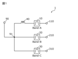
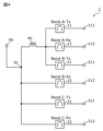
- FIG. 1 is a circuit configuration diagram of a multiplexer according to an embodiment.
- FIG. 2A is a diagram illustrating a first example of a circuit configuration of an elastic wave filter that constitutes a multiplexer according to an embodiment
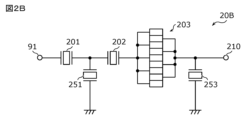
- FIG. 2B is a diagram illustrating a second example of a circuit configuration of an elastic wave filter that constitutes the multiplexer according to the embodiment
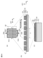
- FIG. 3A is a plan view and a cross-sectional view schematically showing a first example of an elastic wave resonator that constitutes the elastic wave filter according to the embodiment.
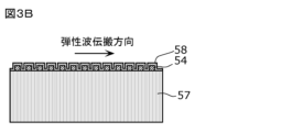
- FIG. 3B is a cross-sectional view schematically showing a second example of the elastic wave resonator that constitutes the elastic wave filter according to the embodiment.
- FIG. 1 is a circuit configuration diagram of a multiplexer according to an embodiment.
- FIG. 2A is a diagram illustrating a first example of a circuit configuration of an elastic wave filter that constitutes a multiplexer according to an embodiment
- FIG. 2B is a diagram illustrating
- FIG. 3C is a cross-sectional view schematically showing a third example of the elastic wave resonator that constitutes the elastic wave filter according to the embodiment.
- FIG. 4 is a circuit configuration diagram of a multiplexer according to the embodiment.
- FIG. 5 is a Smith chart showing impedance characteristics seen from the common terminal of the acoustic wave filter to which the first inductor element according to the example is connected.
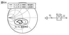
- FIG. 6A is a Smith chart showing impedance characteristics viewed from a common terminal of a single first acoustic wave filter (filter 22) according to the example and the comparative example.
- FIG. 6B is a Smith chart showing impedance characteristics viewed from the common terminal of the elastic wave filter (filter 31) alone according to the example and the comparative example.
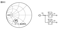
- FIG. 6C is a Smith chart showing impedance characteristics seen from the common terminal of the elastic wave filter (filter 32) alone according to the example and the comparative example.
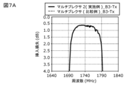
- FIG. 7A is a graph comparing pass characteristics of elastic wave filters (filters 11) of multiplexers according to an example and a comparative example.
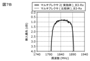
- FIG. 7B is a graph comparing pass characteristics of elastic wave filters (filters 12) of the multiplexers according to the example and the comparative example.
- FIG. 7C is a graph comparing pass characteristics of elastic wave filters (filters 21) of the multiplexers according to the example and the comparative example.
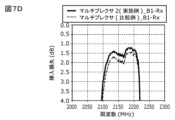
- FIG. 7D is a graph comparing pass characteristics of elastic wave filters (filters 22) of the multiplexers according to the example and the comparative example.
- FIG. 7A is a graph comparing pass characteristics of elastic wave filters (filters 11) of multiplexers according to an example and a comparative example.
- FIG. 7B is a graph comparing pass characteristics of elastic wave filters (filters 12) of the
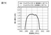
- FIG. 7E is a graph comparing the pass characteristics of the elastic wave filters (filters 31) of the multiplexers according to the example and the comparative example.
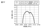
- FIG. 7F is a graph comparing pass characteristics of elastic wave filters (filters 32) of the multiplexers according to the example and the comparative example.
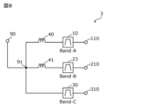
- FIG. 8 is a circuit configuration diagram of a multiplexer according to a modification.
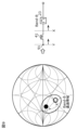
- FIG. 9 is a Smith chart showing the impedance (admittance) of the second inductance element and the first acoustic wave filter according to the modification as seen from the common terminal.
- the passband of the filter is defined as the frequency band between two frequencies that are 3 dB larger than the minimum value of the insertion loss in the passband.
- FIG. 1 is a circuit configuration diagram of a multiplexer 1 according to an embodiment. As shown in the figure, multiplexer 1 includes filters 10 , 20 and 30 , inductor 40 , antenna connection terminal 90 , common terminal 91 , and input/output terminals 110 , 210 and 310 .
- the antenna connection terminal 90 is connected to, for example, an antenna element.
- Common terminal 91 is connected to one end (first end) of inductor 40 , one end of filter 20 , and one end of filter 30 .
- the inductor 40 is an example of a first inductance element and has one end (first end) and the other end (second end). One end (first end) of the inductor 40 is connected to the common terminal 91 and the other end (second end) is connected to one end of the filter 10 .
- the filter 10 is one of one or more acoustic wave filters connected to the other end (second end) of the inductor 40, and has a passband including at least part of band A. One end of the filter 10 is connected to the other end (second end) of the inductor 40 and the other end of the filter 10 is connected to the input/output terminal 110 .
- Filter 10 has one or more elastic wave resonators.
- the filter 20 is one of two or more acoustic wave filters connected to the common terminal 91 without going through the inductor 40, and has a passband including at least part of the band B. One end of the filter 20 is connected to the common terminal 91 and the other end of the filter 20 is connected to the input/output terminal 210 .
- Filter 20 has one or more elastic wave resonators. Further, the filter 20 is an example of a first acoustic wave filter, and among two or more acoustic wave filters connected to the common terminal 91 without the inductor 40, the filter whose passband is located on the lowest frequency side. is.
- the filter 30 is one of two or more acoustic wave filters connected to the common terminal 91 without passing through the inductor 40, and has a passband including at least part of the band C. One end of the filter 30 is connected to the common terminal 91 and the other end of the filter 30 is connected to the input/output terminal 310 . Filter 30 has one or more elastic wave resonators.
- band B is located on the lower frequency side than band C. That is, the passband of the filter 20 is positioned on the lower frequency side than the passband of the filter 30 .
- the passband of band A may be positioned on the lower frequency side or on the higher frequency side than the passband of band B. Also, the passband of band A may be located on the lower frequency side or the higher frequency side than the passband of band C.
- the impedance in the passband of the filter 10 shows inductivity.
- the passband of the filter 20 located on the low-frequency side is The average value of conductance is greater than the average value of conductance in the passband of filter 30 when filter 30 is seen alone from the common terminal 91 side.
- the conductance of the filter 20 is the largest among the conductances in the passbands of the filters 20 and 30, and the transmission by the common connection of the filter 20 is Losses can be large.
- the conductance of filter 20 is maximized. can be reduced. Therefore, the multiplexer 1 with reduced insertion loss can be provided.
- band A for example, LTE (Long Term Evolution) Band 3 (uplink operating band: 1710-1785 MHz, downlink operating band: 1805-1880 MHz) is applied.
- band B for example, Band 1 of LTE (uplink operating band: 1920-1980 MHz, downlink operating band: 2110-2170 MHz) is applied.
- Band 7 of LTE uplink operating band: 2500-2570 MHz, downlink operating band: 2620-2690 MHz
- band C for example.
- the number of filters connected to the other end (second end) of the inductor 40 may be two or more. Also, the number of filters connected to the common terminal 91 without the inductor 40 may be three or more.
- the antenna connection terminal 90 and the input/output terminals 110, 210 and 310 may not be included in the multiplexer 1.
- FIG. 2A is a diagram showing a first example of the circuit configuration of the filter 20 according to the embodiment.
- FIG. 2B is a diagram showing a second example of the circuit configuration of the filter 20 according to the embodiment.
- the filter 20 according to the present embodiment has, for example, the circuit configuration of the elastic wave filter 20A shown in FIG. 2A or the elastic wave filter 20B shown in FIG. 2B.
- Filters 10 and 30 may also have the circuit configuration of elastic wave filter 20A shown in FIG. 2A or elastic wave filter 20B shown in FIG. 2B.
- the acoustic wave filter 20A shown in FIG. 2A includes series arm resonators 101 to 105, parallel arm resonators 151 to 154, and an inductor 161.
- the series arm resonators 101 to 105 are arranged on a series arm path connecting the input/output terminal 210 and the common terminal 91 .
- Each of the parallel arm resonators 151 to 154 is connected between each connection point of the series arm resonators 101 to 105 and the input/output terminal 210 and the ground.
- the elastic wave filter 20A constitutes a ladder-type bandpass filter.
- Inductor 161 is connected between the connection point of parallel arm resonators 151, 152 and 153 and the ground, and adjusts the attenuation pole in the filter pass characteristics.
- the number of series arm resonators and parallel arm resonators is arbitrary, and inductor 161 may be omitted.
- the elastic wave filter 20B shown in FIG. 2B includes a longitudinally coupled filter section 203, series arm resonators 201 and 202, and parallel arm resonators 251 and 253.
- the longitudinal coupling filter unit 203 has, for example, nine IDTs, each of which is composed of a pair of IDT electrodes facing each other.
- Series arm resonators 201 and 202 and parallel arm resonator 251 constitute a ladder filter section.
- the acoustic wave filter 20B constitutes a bandpass filter.
- elastic wave filter 20B shown as the second example of filter 20 the number of series arm resonators and parallel arm resonators and the number of IDTs constituting longitudinally coupled filter section 203 are arbitrary.
- FIG. 3A is a plan view and a cross-sectional view schematically showing a first example of elastic wave resonators of filters 10, 20 and 30 according to the embodiment.
- the figure illustrates the basic structure of elastic wave resonators forming filters 10 , 20 and 30 .
- the elastic wave resonator 60 shown in FIG. 3A is for explaining a typical structure of an elastic wave resonator, and the number and length of the electrode fingers constituting the electrodes are Not limited.
- the acoustic wave resonator 60 is composed of a piezoelectric substrate 50 and comb electrodes 60a and 60b.
- a pair of comb electrodes 60a and 60b facing each other are formed on the substrate 50.
- the comb-shaped electrode 60a is composed of a plurality of parallel electrode fingers 61a and busbar electrodes 62a connecting the plurality of electrode fingers 61a.
- the comb-shaped electrode 60b is composed of a plurality of parallel electrode fingers 61b and a busbar electrode 62b connecting the plurality of electrode fingers 61b.
- the plurality of electrode fingers 61a and 61b are formed along a direction orthogonal to the elastic wave propagation direction (X-axis direction).
- the IDT electrode 54 which is composed of a plurality of electrode fingers 61a and 61b and busbar electrodes 62a and 62b, has a laminated structure of an adhesion layer 540 and a main electrode layer 542, as shown in (b) of FIG. 3A. It's becoming
- the adhesion layer 540 is a layer for improving adhesion between the substrate 50 and the main electrode layer 542, and is made of Ti, for example.
- the material of the main electrode layer 542 is, for example, Al containing 1% Cu.
- Protective layer 55 is formed to cover comb electrodes 60a and 60b.
- the protective layer 55 is a layer for the purpose of protecting the main electrode layer 542 from the external environment, adjusting frequency temperature characteristics, and increasing moisture resistance. is.
- the materials forming the adhesion layer 540, the main electrode layer 542 and the protective layer 55 are not limited to the materials described above.
- the IDT electrode 54 may not have the laminated structure described above.
- the IDT electrode 54 may be composed of, for example, metals or alloys such as Ti, Al, Cu, Pt, Au, Ag, and Pd, and may be composed of a plurality of laminates composed of the above metals or alloys. may Also, the protective layer 55 may not be formed.
- the substrate 50 includes a high acoustic velocity supporting substrate 51, a low acoustic velocity film 52, and a piezoelectric film 53.
- the high acoustic velocity supporting substrate 51, the low acoustic velocity film 52, and the piezoelectric film 53 are It has a structure laminated in this order.
- the piezoelectric film 53 is, for example, a ⁇ ° Y-cut X-propagation LiTaO 3 piezoelectric single crystal or a piezoelectric ceramic (lithium tantalate single crystal cut along a plane normal to an axis rotated ⁇ ° from the Y axis with the X axis as the central axis, (or ceramics, single crystal or ceramics in which surface acoustic waves propagate in the X-axis direction). Note that the material of the piezoelectric single crystal used as the piezoelectric film 53 and the cut angle ⁇ are appropriately selected according to the required specifications of each filter.
- the high acoustic velocity support substrate 51 is a substrate that supports the low acoustic velocity film 52 , the piezoelectric film 53 and the IDT electrodes 54 .
- the high acoustic velocity support substrate 51 is a substrate in which the acoustic velocity of bulk waves in the high acoustic velocity support substrate 51 is faster than acoustic waves such as surface waves and boundary waves propagating through the piezoelectric film 53, and surface acoustic waves are generated. It functions so that it is confined in the portion where the piezoelectric film 53 and the low sound velocity film 52 are laminated and does not leak below the high sound velocity support substrate 51 .
- the high acoustic velocity support substrate 51 is, for example, a silicon substrate.
- the low sound velocity film 52 is a film in which the sound velocity of the bulk wave in the low sound velocity film 52 is lower than that of the bulk wave propagating through the piezoelectric film 53 , and is arranged between the piezoelectric film 53 and the high sound velocity support substrate 51 . be.
- This structure and the nature of the elastic wave to concentrate its energy in a low-temperature medium suppresses leakage of the surface acoustic wave energy to the outside of the IDT electrode.
- the low-temperature velocity film 52 is, for example, a film whose main component is silicon dioxide.
- the laminated structure of the substrate 50 it is possible to significantly increase the Q value at the resonance frequency and anti-resonance frequency compared to the conventional structure using a single layer piezoelectric substrate. That is, since an acoustic wave resonator with a high Q value can be configured, it is possible to configure a filter with a small insertion loss using the acoustic wave resonator.
- the high acoustic velocity support substrate 51 has a structure in which a support substrate and a high acoustic velocity film having a higher acoustic velocity than elastic waves such as surface waves and boundary waves propagating through the piezoelectric film 53 are laminated.
- the support substrate includes piezoelectric materials such as sapphire, lithium tantalate, lithium niobate, and quartz, alumina, magnesia, silicon nitride, aluminum nitride, silicon carbide, zirconia, cordierite, mullite, steatite, and fort.
- the high acoustic velocity film includes aluminum nitride, aluminum oxide, silicon carbide, silicon nitride, silicon oxynitride, DLC film, diamond, media containing these materials as main components, and media containing mixtures of these materials as main components. etc., various high acoustic velocity materials can be used.
- FIG. 3B is a cross-sectional view schematically showing a second example of elastic wave resonators of filters 10, 20 and 30 according to the embodiment.
- the elastic wave resonator 60 shown in FIG. 3A shows an example in which the IDT electrodes 54 are formed on the substrate 50 having the piezoelectric film 53.
- the substrate on which the IDT electrodes 54 are formed is shown in FIG. 3B.
- the piezoelectric single crystal substrate 57 may be a single piezoelectric layer.
- the piezoelectric single crystal substrate 57 is composed of, for example, a piezoelectric single crystal of LiNbO 3 .
- the acoustic wave resonator according to this example is composed of a piezoelectric single crystal substrate 57 of LiNbO 3 , an IDT electrode 54 , and a protective layer 58 formed on the piezoelectric single crystal substrate 57 and the IDT electrode 54 . .
- the piezoelectric film 53 and the piezoelectric single crystal substrate 57 described above may be appropriately changed in laminated structure, material, cut angle, and thickness according to the required transmission characteristics of the elastic wave filter device. Even an elastic wave resonator using a LiTaO 3 piezoelectric substrate having a cut angle other than the cut angle described above can produce the same effects as the elastic wave resonator 60 using the piezoelectric film 53 described above.
- the substrate on which the IDT electrodes 54 are formed may have a structure in which a supporting substrate, an energy trapping layer, and a piezoelectric film are laminated in this order.
- An IDT electrode 54 is formed on the piezoelectric film.
- the piezoelectric film is, for example, LiTaO 3 piezoelectric single crystal or piezoelectric ceramics.
- the support substrate is the substrate that supports the piezoelectric film, the energy confinement layer, and the IDT electrodes 54 .
- the energy confinement layer consists of one or more layers, and the velocity of the bulk acoustic wave propagating through at least one layer is greater than the velocity of the elastic wave propagating near the piezoelectric film.
- the energy trapping layer may have a laminated structure of a low acoustic velocity layer and a high acoustic velocity layer.
- the sound velocity layer is a film in which the sound velocity of bulk waves in the sound velocity layer is lower than the sound velocity of elastic waves propagating through the piezoelectric film.
- the high acoustic velocity layer is a film in which the acoustic velocity of bulk waves in the high acoustic velocity layer is higher than the acoustic velocity of elastic waves propagating through the piezoelectric film.
- the support substrate may be a high acoustic velocity layer.
- the energy trapping layer may be an acoustic impedance layer having a configuration in which a low acoustic impedance layer with a relatively low acoustic impedance and a high acoustic impedance layer with a relatively high acoustic impedance are alternately laminated. .
- the wavelength of the elastic wave resonator is defined by the wavelength ⁇ which is the repetition period of the plurality of electrode fingers 61a or 61b forming the IDT electrode 54 shown in (b) of FIG. 3A.
- the electrode finger pitch is 1/2 of the wavelength ⁇
- the line width of the electrode fingers 61a and 61b constituting the comb-shaped electrodes 60a and 60b is W
- the distance between the adjacent electrode fingers 61a and 61b is When the space width is S, it is defined as (W+S).
- S space width
- the intersecting width L of the pair of comb-shaped electrodes 60a and 60b is the overlap of the electrode fingers 61a and 61b when viewed from the elastic wave propagation direction (X-axis direction). is the length of the electrode finger that
- the electrode duty of each acoustic wave resonator is the line width occupation ratio of the plurality of electrode fingers 61a and 61b, and is the ratio of the line width to the sum of the line width and space width of the plurality of electrode fingers 61a and 61b. and is defined as W/(W+S).
- the height of the comb electrodes 60a and 60b is h.
- electrode parameters related to the shape of the IDT electrodes of the acoustic wave resonator such as the wavelength ⁇ , the electrode finger pitch, the crossing width L, the electrode duty, and the height h of the IDT electrodes 54, are defined as electrode parameters.
- the electrode finger pitch of the IDT electrodes 54 is defined by the average electrode finger pitch of the IDT electrodes 54 .
- the average electrode finger pitch of the IDT electrode 54 is defined by the total number of the electrode fingers 61a and 61b included in the IDT electrode 54 being Ni, and the electrode finger positioned at one end of the IDT electrode 54 in the elastic wave propagation direction and It is defined as Di/(Ni-1), where Di is the center-to-center distance from the positioned electrode finger.
- the resonance frequency and antiresonance frequency of the surface acoustic wave resonator shift to the lower frequency side as the electrode finger pitch of the IDT electrode increases. shift.
- FIG. 3C is a cross-sectional view schematically showing a third example of elastic wave resonators of filters 10, 20 and 30 according to the embodiment.
- Bulk acoustic wave resonators are shown as acoustic wave resonators of filters 10, 20 and 30 in FIG. 3C.
- the bulk acoustic wave resonator has, for example, a support substrate 65, a lower electrode 66, a piezoelectric layer 67, and an upper electrode 68. , a piezoelectric layer 67, and an upper electrode 68 are laminated in this order.
- the support substrate 65 is a substrate for supporting the lower electrode 66, the piezoelectric layer 67, and the upper electrode 68, and is, for example, a silicon substrate.
- the support substrate 65 is provided with a cavity in a region in contact with the lower electrode 66 . This allows the piezoelectric layer 67 to vibrate freely.
- the lower electrode 66 is an example of a first electrode and is formed on one surface of the support substrate 65 .
- the upper electrode 68 is an example of a second electrode and is formed on one surface of the support substrate 65 .
- the lower electrode 66 and the upper electrode 68 are made of Al containing 1% Cu, for example.
- the piezoelectric layer 67 is formed between the lower electrode 66 and the upper electrode 68 .
- the piezoelectric layer 67 is made of, for example, ZnO (zinc oxide), AlN (aluminum nitride), PZT (lead zirconate titanate), KN (potassium niobate), LN (lithium niobate), LT (lithium tantalate),
- the main component is at least one of quartz and LiBO (lithium borate).
- the bulk acoustic wave resonator having the above laminated structure induces a bulk acoustic wave in the piezoelectric layer 67 by applying electrical energy between the lower electrode 66 and the upper electrode 68 to generate resonance. It is.
- a bulk acoustic wave generated by this bulk acoustic wave resonator propagates between the lower electrode 66 and the upper electrode 68 in a direction perpendicular to the film surface of the piezoelectric layer 67 . That is, the bulk acoustic wave resonator is a resonator that utilizes bulk acoustic waves.
- the resonance frequency and anti-resonance frequency of the bulk acoustic wave resonator shift to the low frequency side.
- each of filters 20 and 30 is composed of one or more surface acoustic wave resonators having IDT electrodes 54, and each of filters 20 and 30 is connected to common terminal 91.
- a series arm resonator arranged on a series arm path connecting the output terminals 210 and 310 may be included.
- the electrode finger pitch of the IDT electrodes 54 forming the series arm resonators included in the filter 20 is It can be the largest.
- the passband of the filter 20 is located on the lowest frequency side.
- each of filters 20 and 30 includes support substrate 65, lower electrode 66 and upper electrode 68 formed on one surface of support substrate 65, lower electrode 66 and upper
- Each of the filters 20 and 30 connects a common terminal 91 and input/output terminals 210 and 310 to each other.
- a series arm resonator arranged on the series arm path may be included.
- the piezoelectric layers 67 forming the series arm resonators included in the filter 20 may be the thickest among the piezoelectric layers 67 forming the series arm resonators included in the filters 20 and 30, respectively.
- the passband of the filter 20 is located on the lowest frequency side.
- FIG. 4 is a circuit configuration diagram of the multiplexer 2 according to the embodiment.
- the multiplexer 2 according to the present embodiment is an example of the multiplexer 1 according to the embodiment, and each of the band A, the band B and the band C has a frequency division duplex (FDD) band. It has an applied configuration.
- FDD frequency division duplex
- the multiplexer 2 includes filters 11, 12, 21, 22, 31 and 32, an inductor 40, an antenna connection terminal 90, a common terminal 91, input terminals 111, 211 and 311, and an output terminals 112, 212 and 312;
- the multiplexer 2 according to the present embodiment has three filters connected to the inductor 40, and three filters connected to the common terminal 91 without the inductor 40. The difference is that
- the description of the same configuration as that of the multiplexer 1 according to the embodiment will be omitted, and the description will focus on the different configuration.
- the antenna connection terminal 90 is connected to, for example, an antenna element.
- Common terminal 91 is connected to one end (first end) of inductor 40 , one end of filter 22 , one end of filter 31 , and one end of filter 32 .
- the inductor 40 is an example of a first inductance element and has one end (first end) and the other end (second end). One end (first end) of inductor 40 is connected to common terminal 91 , and the other end (second end) is connected to one end of filter 11 , one end of filter 12 , and one end of filter 21 .
- the filter 11 is one of one or more acoustic wave filters connected to the other end (second end) of the inductor 40, and has a passband that includes the Band A uplink operating band. One end of the filter 11 is connected to the other end (second end) of the inductor 40 and the other end of the filter 11 is connected to the input terminal 111 . Filter 11 has one or more elastic wave resonators.
- the filter 12 is one of one or more acoustic wave filters connected to the other end (second end) of the inductor 40 and has a passband that includes the Band A downlink operating band. One end of the filter 12 is connected to the other end (second end) of the inductor 40 and the other end of the filter 12 is connected to the output terminal 112 .
- Filter 12 has one or more elastic wave resonators.
- the filter 21 is one of one or more acoustic wave filters connected to the other end (second end) of the inductor 40, and has a passband including the band B uplink operating band. One end of the filter 21 is connected to the other end (second end) of the inductor 40 and the other end of the filter 21 is connected to the input terminal 211 .
- Filter 21 has one or more elastic wave resonators.
- Filter 22 is one of two or more acoustic wave filters connected to common terminal 91 without inductor 40 and has a passband that includes Band B downlink operating band. One end of the filter 22 is connected to the common terminal 91 and the other end of the filter 22 is connected to the output terminal 212 . Filter 22 has one or more elastic wave resonators. Further, the filter 22 is an example of a first acoustic wave filter, and among two or more acoustic wave filters connected to the common terminal 91 without the inductor 40, the filter whose pass band is located on the lowest frequency side. is.
- the filter 31 is one of two or more acoustic wave filters connected to the common terminal 91 without going through the inductor 40, and has a passband that includes the Band C uplink operating band. One end of the filter 31 is connected to the common terminal 91 and the other end of the filter 31 is connected to the input terminal 311 . Filter 31 has one or more elastic wave resonators.
- Filter 32 is one of two or more acoustic wave filters connected to common terminal 91 without inductor 40 and has a passband that includes band C downlink operating band. One end of the filter 32 is connected to the common terminal 91 and the other end of the filter 32 is connected to the output terminal 312 . Filter 32 has one or more elastic wave resonators.
- the uplink operating band means the frequency range designated for the uplink among the above bands.
- the downlink operating band means the frequency range designated for the downlink among the above bands.
- the downlink operating band of band B is located on the lower frequency side than the uplink operating band and downlink operating band of band C. That is, the passband of filter 22 is located on the lower frequency side than the passbands of filters 31 and 32 .
- Band 3 of LTE is applied as band A
- Band 1 of LTE is applied as band B
- Band 7 of LTE is applied as band C.
- FIG. 5 is a Smith chart showing impedance characteristics viewed from the common terminal 91 of the filters 11, 12 and 21 to which the inductor 40 according to the embodiment is connected. More specifically, FIG. 5 shows the impedance of the filters 11, 12 and 21 connected to the inductor 40 viewed from the common terminal 91 when the filters 22, 31 and 32 are not connected to the common terminal 91. It is shown. As shown in the figure, the impedance in each passband of filters 11, 12 and 21 (B3-Tx passband, B3-Rx passband and B1-Tx passband in FIG. 5) shows inductivity. Since each of the filters 11, 12 and 21 is an acoustic wave filter, the impedance of each single filter 11, 12 and 21 exhibits capacitiveness.
- the impedance of the filters 11, 12 and 21 viewed from the common terminal 91 side with the inductor 40 not connected exhibits capacitiveness.
- the impedance of the filters 11, 12 and 21 viewed from the common terminal 91 side is equal to the Smith chart equal resistance Shift clockwise on the circle.
- the impedance in each passband when filters 11, 12 and 21 to which inductor 40 is connected is viewed from common terminal 91 shifts from the capacitive region to the inductive region.
- the impedance in the passbands of the filters 22, 31 and 32 (B1-Rx attenuation band and B7 attenuation band in FIG. 5) is Located at the outer edge of the inductive region. This is due to the following effects.
- the impedance in the passband of filters 22, 31 and 32 is located at the outer edge of the capacitive region.
- the impedance in the passband of the filters 22, 31 and 32 is shifted clockwise on the equal resistance circle of the Smith chart. shift.
- the impedance in the passband of the filters 22, 31 and 32 becomes more open as the frequency becomes higher (the B7 attenuation band in FIG. 5).
- the lower the frequency (the B1-Rx attenuation band in FIG. 5) the closer to the short side.
- the conductance in the passbands of the filters 22, 31 and 32 decreases as the frequency increases (B7 attenuation band in FIG. 5).
- the conductance ( The B1-Rx attenuation band in FIG. 5) is large compared to the conductance in the passbands of filters 31 and 32 (B7 attenuation band in FIG. 5). Therefore, there is a concern that the received signal of Band 1, which should pass through filter 22, is likely to leak to filters 11, 12 and 21, increasing the transmission loss of filter 22.
- FIG. 5 shows that the conductance ( The B1-Rx attenuation band in FIG. 5) is large compared to the conductance in the passbands of filters 31 and 32 (B7 attenuation band in FIG. 5). Therefore, there is a concern that the received signal of Band 1, which should pass through filter 22, is likely to leak to filters 11, 12 and 21, increasing the transmission loss of filter 22.
- the average conductance in the passband of the filter 22 is The value is set larger than the average value of the conductance in each passband when the filter 31 alone and the filter 32 alone are viewed from the common terminal 91 .
- FIG. 6A is a Smith chart showing impedance characteristics viewed from the common terminal 91 of the single filter 22 according to the example and the comparative example.
- FIG. 6B is a Smith chart showing impedance characteristics of the filters 31 according to the example and the comparative example viewed from the common terminal 91 .
- FIG. 6C is a Smith chart showing impedance characteristics of the filters 32 according to the example and the comparative example viewed from the common terminal 91 . More specifically, FIG. 6A shows the admittance in the passband of the filter 22 when the filter 22 alone is viewed from the common terminal 91 in the example and the comparative example, and FIG.
- the admittance in the passband of the filter 31 when the filters 31 and 32 connected to the common terminal 91 are viewed from the common terminal 91 is shown.
- the admittance in the passband of filter 32 when filters 31 and 32 connected to common terminal 91 are viewed from common terminal 91 is shown.
- FIG. 6B and 6C show the admittance when the filters 31 and 32 are commonly connected, but the admittance in the passband of the filter 31 when the filter 31 alone is viewed from the common terminal 91 is It lies on the conductance circle outside the admittance shown in FIG. 6B. Also, the admittance in the pass band of the filter 32 when the single filter 32 is viewed from the common terminal 91 is located in the conductance circle outside the admittance shown in FIG. 6C.
- each of the filters 11, 12, 21, 22, 31 and 32 according to the comparative example is a filter having an electrode parameter that minimizes the insertion loss in the passband of each individual filter.
- the average value of the conductance in the passband of filter 22 when viewed from common terminal 91 is Larger than the average value of the conductance in the passband of the filter 31 when viewed from the common terminal 91 side, and larger than the average value of the conductance in the passband of the filter 32 when the single filter 32 is viewed from the common terminal 91 side big.
- the average value of the conductance in the passband when the filter 22 is seen alone from the common terminal 91 side is the conductance in the passband when each of the filters 22, 31 and 32 is seen alone from the common terminal 91 side. is the largest among the average values of
- the conductance of the filter 22 among the conductances in the passbands of the filters 22, 31 and 32 is It is the largest, and there is a possibility that the transmission loss due to the common connection of the filters 22 will increase.
- the conductance of filter 22 is the largest among the conductances in the passband when each of filters 22 , 31 and 32 is viewed from common terminal 91 .
- the reception signal of Band 1 can be suppressed from leaking to the filters 11, 12 and 21, and the transmission loss due to the common connection of the filter 22 can be reduced. Therefore, the multiplexer 2 with reduced insertion loss can be provided.
- the impedance in the passband of each filter when the filters 11, 12 and 21 connected to the common terminal 91 via the inductor 40 are viewed from the common terminal 91 is shown in FIG. Located in the inducible region as indicated.
- the impedance in the passband of each filter is located in the capacitive region (Figs. 6A and 6B and FIG. 6C).
- the impedance seen from the common terminal 91 of each filter is the reference impedance (eg 50 ⁇ ).
- FIG. 7A is a graph comparing the pass characteristics of the filters 11 of the multiplexers according to the example and the comparative example.
- FIG. 7B is a graph comparing the pass characteristics of the filters 12 of the multiplexers according to the example and the comparative example.
- FIG. 7C is a graph comparing pass characteristics of the filters 21 of the multiplexers according to the example and the comparative example.
- FIG. 7D is a graph comparing pass characteristics of the filters 22 of the multiplexers according to the example and the comparative example.
- FIG. 7E is a graph comparing the pass characteristics of the filters 31 of the multiplexers according to the example and the comparative example.
- FIG. 7F is a graph comparing the pass characteristics of the filters 32 of the multiplexers according to the example and the comparative example.
- FIGS. 7A, 7B, 7C, 7E and 7F there is no difference between the pass characteristics of the filters 11, 12, 21, 31 and 32 in the multiplexer between the example and the comparative example.
- FIG. 7D in the filter 22 in the multiplexer, the insertion loss within the passband is significantly reduced in the example compared to the comparative example. That is, the multiplexer 2 according to the embodiment has a reduced insertion loss compared to the multiplexer according to the comparative example.
- the passbands of the filters 11, 12 and 21 are located on the lower frequency side than the passbands of the filters 22, 31 and 32.
- the filters 11, 12 and 21 are viewed from the common terminal 91, the amount by which the admittance in the passband of the filters 22, 31 and 32 is shifted by the inductor 40 in the direction of decreasing the conductance increases. Therefore, loss due to common connection of the filters 22, 31 and 32 can be further reduced.
- the multiplexer 2 has a plurality of filters connected to the inductor 40 .
- the impedances in the passbands of the filters 11, 12 and 21 are located on the capacitive side compared to the case where one filter is connected to the inductor 40. Therefore, the amount of shift of the conductance of the admittance of the filters 11, 12 and 21 in the passbands of the filters 22, 31 and 32 due to the series connection of the inductor 40 is increased. Therefore, loss due to common connection of the filters 22, 31 and 32 can be further reduced.
- FIG. 8 is a circuit configuration diagram of the multiplexer 3 according to the modification.
- the multiplexer 3 includes filters 10 , 23 and 30 , inductors 40 and 41 , an antenna connection terminal 90 , a common terminal 91 , and input/output terminals 110 , 210 and 310 .
- a multiplexer 3 according to this modification differs from the multiplexer 1 according to the embodiment in that a filter 23 and an inductor 41 are arranged instead of the filter 20 .
- the description of the same configuration as that of the multiplexer 1 according to the embodiment will be omitted, and the different configuration will be mainly described.
- the common terminal 91 is connected to one end (first end) of the inductor 40 , one end of the inductor 41 and one end of the filter 30 .
- the inductor 40 is an example of a first inductance element and has one end (first end) and the other end (second end). One end (first end) of the inductor 40 is connected to the common terminal 91 and the other end (second end) is connected to one end of the filter 10 .
- the inductor 41 is an example of a second inductance element, and is connected in series with the filter 23 between the common terminal 91 and the filter 23 . That is, one end of the inductor 41 is connected to the common terminal 91 and the other end is connected to the filter 23 .
- the inductance value of inductor 41 is smaller than the inductance value of inductor 40 .
- the filter 23 is one of two or more acoustic wave filters connected to the common terminal 91 via the inductor 41, and has a passband including at least part of band B. One end of the filter 23 is connected to the other end of the inductor 41 and the other end of the filter 23 is connected to the input/output terminal 210 .
- Filter 23 has one or more elastic wave resonators. Further, the filter 23 is an example of a first acoustic wave filter, and among two or more acoustic wave filters connected to the common terminal 91 without the inductor 40, the filter whose pass band is located on the lowest frequency side. is.
- band B is located on the lower frequency side than band C. That is, the passband of the filter 23 is positioned on the lower frequency side than the passband of the filter 30 .
- the impedance in the passband of the filter 10 shows inductivity.
- the average value of the conductance in the passband of the filter 23 is is greater than the average value of the conductance in the passband of filter 30 when
- FIG. 9 is a Smith chart showing the impedance (admittance) of the inductor 41 and the filter 23 according to the modification viewed from the common terminal 91.
- FIG. 9 As shown in the figure, the admittance in the passband of the filter 23 when the filter 23 alone to which the inductor 41 is not connected is viewed from the common terminal 91 side (X in FIG. 9) is located in the capacitive region.
- the admittance in the passband of the filter 23 when the filter 23 with the inductor 41 connected in series is viewed from the common terminal 91 (Y in FIG. 9) shifts the equal resistance circle clockwise, so that the conductance becomes higher. Shifting to the large capacitive region.
- the average value of the conductance in the passband of the filter 23 when the filter 23 is viewed from the common terminal 91 while the filter 30 is not connected to the common terminal 91 is It is larger than the average value of the conductance in the passband of the filter 30 when the filter 30 is seen alone from the common terminal 91 side.
- the inductance value of the inductor 41 is smaller than the inductance value of the inductor 40, the admittance in the passband when viewed from the common terminal 91 of the filter 23 to which the inductor 41 is connected is not shifted to the inductive region, and the capacitance It is possible to keep it in the sexual area.
- the impedances of the filters 11, 12 and 21 and the impedances of the filters 22, 31 and 32 viewed from the common terminal 91 can be in a complex conjugate relationship.
- the impedance in the passband when the filter 23 is viewed from the common terminal 91 is maintained capacitive by the inductor 41, and the conductance in the passband when the filter 23 is viewed from the common terminal 91 is reduced by the filter. It is possible to achieve a high conductance value that cannot be achieved by design adjustment of the electrode parameters of the acoustic wave resonator constituting 23 .
- the multiplexer 1 includes the common terminal 91, the inductor 40 having one end connected to the common terminal 91, the filter 10 connected to the other end of the inductor 40, and the inductor 40 and the filters 20 and 30 are connected to the common terminal 91 without passing through the common terminal 91, and the filter 10 connected to the inductor 40 is viewed from the common terminal 91 in a state in which the filters 20 and 30 are not connected to the common terminal 91.
- the impedance in the passband of filter 10 in this case is inductive. In this state, the average value of the conductance in the passband when viewed from the common terminal 91 is larger than the average value of the conductance in the passband when the filter 30 alone is viewed from the common terminal 91 .
- the conductance of the filter 20 is the largest among the conductances in the passbands of the filters 20 and 30, and the transmission by the common connection of the filter 20 is Losses can be large.
- the conductance of filter 20 is maximized. can be reduced. Therefore, the multiplexer 1 with reduced insertion loss can be provided.
- the passbands of the filters 11, 12 and 21 may be located on the lower frequency side than the passbands of the filters 22, 31 and 32.
- the filters 11, 12 and 21 are viewed from the common terminal 91, the amount by which the admittance in the passband of the filters 22, 31 and 32 is shifted by the inductor 40 in the direction of decreasing the conductance increases. Therefore, loss due to common connection of the filters 22, 31 and 32 can be further reduced.
- the multiplexer 2 may have a plurality of filters connected to the inductor 40 .
- the impedances in the passbands of the filters 11, 12 and 21 are located on the capacitive side compared to the case where one filter is connected to the inductor 40. Therefore, the amount of shift of the admittance in the passbands of the filters 22, 31 and 32 in the direction in which the conductance becomes smaller due to the series connection of the inductor 40 increases. Therefore, loss due to common connection of the filters 22, 31 and 32 can be further reduced.
- the multiplexer 3 further includes an inductor 41 connected in series with the filter 23 between the common terminal 91 and the filter 23, and the inductance value of the inductor 41 is smaller than the inductance value of the inductor 40.
- the impedance in the passband when the filter 23 is viewed from the common terminal 91 is maintained capacitive by the inductor 41, and the conductance in the passband when the filter 23 is viewed from the common terminal 91 is reduced by the filter. It is possible to achieve a high conductance value that cannot be achieved by design adjustment of the elastic wave resonator constituting 23 .
- each of filters 20 and 30 is composed of one or more surface acoustic wave resonators having IDT electrodes 54, and each of filters 20 and 30 is connected to common terminal 91.
- a series arm resonator arranged on a series arm path connecting the output terminals 210 and 310 may be included.
- the electrode finger pitch of the IDT electrodes 54 forming the series arm resonators included in the filter 20 is It can be the largest.
- the passband of the filter 20 can be located on the lowest frequency side.
- each of filters 20 and 30 includes support substrate 65, lower electrode 66 and upper electrode 68 formed on one surface of support substrate 65, lower electrode 66 and upper electrode 68, and lower electrode 66 and upper electrode 68.
- Each of the filters 20 and 30 connects a common terminal 91 and input/output terminals 210 and 310 to each other.
- a series arm resonator arranged on the series arm path may be included.
- the piezoelectric layers 67 forming the series arm resonators included in the filter 20 may be the thickest among the piezoelectric layers 67 forming the series arm resonators included in the filters 20 and 30, respectively.
- the passband of the filter 20 can be located on the lowest frequency side.
- matching elements such as inductors and capacitors, and switch circuits may be connected between the constituent elements.
- the inductor may include a wiring inductor that is a wiring that connects each component.
- the present invention can be widely used in communication equipment such as mobile phones as a low-loss multiplexer applicable to multi-band and multi-mode frequency standards.
Landscapes
- Physics & Mathematics (AREA)
- Acoustics & Sound (AREA)
- Surface Acoustic Wave Elements And Circuit Networks Thereof (AREA)
Abstract
La présente divulgation concerne un multiplexeur (1) qui comprend une borne partagée (91), un inducteur (40) ayant une extrémité connectée à la borne partagée (91), un filtre (10) connecté à l'autre extrémité de l'inducteur (40), et des filtres (20 et 30) connectés à la borne partagée (91) sans traverser l'inducteur (40). L'impédance dans la bande passante lorsque le filtre (10) auquel l'inducteur (40) est connecté est vue depuis la borne partagée (91) tandis que les filtres (20 et 30) ne sont pas connectés à la borne partagée (91) présente une inductivité. La valeur moyenne de la conductance dans la bande passante lorsque le filtre (20) positionné sur le côté basse fréquence des filtres (20 et 30) est vu à partir de la borne partagée (91) tandis que les filtres (10 et 30) ne sont pas connectés à la borne partagée (91) est plus grande que la valeur moyenne de la conductance dans la bande passante lorsque le filtre (30) seul est vu depuis la borne partagée (91).
Applications Claiming Priority (2)
| Application Number | Priority Date | Filing Date | Title |
|---|---|---|---|
| JP2021-187021 | 2021-11-17 | ||
| JP2021187021 | 2021-11-17 |
Publications (1)
| Publication Number | Publication Date |
|---|---|
| WO2023090238A1 true WO2023090238A1 (fr) | 2023-05-25 |
Family
ID=86396888
Family Applications (1)
| Application Number | Title | Priority Date | Filing Date |
|---|---|---|---|
| PCT/JP2022/041836 Ceased WO2023090238A1 (fr) | 2021-11-17 | 2022-11-10 | Multiplexeur |
Country Status (1)
| Country | Link |
|---|---|
| WO (1) | WO2023090238A1 (fr) |
Citations (4)
| Publication number | Priority date | Publication date | Assignee | Title |
|---|---|---|---|---|
| JPH1168511A (ja) * | 1997-08-22 | 1999-03-09 | Murata Mfg Co Ltd | 弾性表面波装置 |
| WO2016111262A1 (fr) * | 2015-01-07 | 2016-07-14 | 株式会社村田製作所 | Dispositif de filtre composite |
| JP2019220877A (ja) * | 2018-06-21 | 2019-12-26 | 株式会社村田製作所 | マルチプレクサ |
| WO2020137263A1 (fr) * | 2018-12-25 | 2020-07-02 | 株式会社村田製作所 | Dispositif de filtrage |
-
2022
- 2022-11-10 WO PCT/JP2022/041836 patent/WO2023090238A1/fr not_active Ceased
Patent Citations (4)
| Publication number | Priority date | Publication date | Assignee | Title |
|---|---|---|---|---|
| JPH1168511A (ja) * | 1997-08-22 | 1999-03-09 | Murata Mfg Co Ltd | 弾性表面波装置 |
| WO2016111262A1 (fr) * | 2015-01-07 | 2016-07-14 | 株式会社村田製作所 | Dispositif de filtre composite |
| JP2019220877A (ja) * | 2018-06-21 | 2019-12-26 | 株式会社村田製作所 | マルチプレクサ |
| WO2020137263A1 (fr) * | 2018-12-25 | 2020-07-02 | 株式会社村田製作所 | Dispositif de filtrage |
Similar Documents
| Publication | Publication Date | Title |
|---|---|---|
| KR102429897B1 (ko) | 멀티플렉서, 고주파 프론트엔드 회로 및 통신 장치 | |
| JP6590069B2 (ja) | マルチプレクサ、高周波フロントエンド回路及び通信装置 | |
| CN109600125B (zh) | 滤波器 | |
| JP6683256B2 (ja) | マルチプレクサ、高周波フロントエンド回路及び通信装置 | |
| KR102316966B1 (ko) | 멀티플렉서 | |
| US20200153414A1 (en) | Multiplexer, radio-frequency (rf) front-end circuit, and communication apparatus | |
| WO2019111902A1 (fr) | Multiplexeur, circuit frontal haute fréquence et dispositif de communication | |
| WO2018003296A1 (fr) | Multiplexeur, circuit frontal haute fréquence et dispositif de communication | |
| JP2020048067A (ja) | エクストラクタ | |
| JP6885526B2 (ja) | フィルタ、マルチプレクサ、高周波フロントエンド回路及び通信装置 | |
| US11855605B2 (en) | Acoustic wave filter device and multiplexer | |
| JPWO2020044979A1 (ja) | フィルタ装置およびマルチプレクサ | |
| US20250175158A1 (en) | Multiplexer | |
| JP2023044392A (ja) | 弾性波素子、弾性波フィルタ装置およびマルチプレクサ | |
| WO2023074373A1 (fr) | Résonateur à ondes élastiques, dispositif de filtre à ondes élastiques et multiplexeur | |
| JP7231007B2 (ja) | フィルタ、マルチプレクサ、高周波フロントエンド回路及び通信装置 | |
| WO2023090238A1 (fr) | Multiplexeur | |
| KR102894141B1 (ko) | 멀티플렉서 | |
| WO2023068206A1 (fr) | Multiplexeur | |
| CN219247815U (zh) | 多工器 | |
| CN221553235U (zh) | 弹性波元件、弹性波滤波器装置及多工器 | |
| JP2024047755A (ja) | マルチプレクサ | |
| WO2023054301A1 (fr) | Dispositif de filtre à ondes élastiques et multiplexeur | |
| JP2024162470A (ja) | マルチプレクサ | |
| JP2025097818A (ja) | 弾性波フィルタ |
Legal Events
| Date | Code | Title | Description |
|---|---|---|---|
| 121 | Ep: the epo has been informed by wipo that ep was designated in this application |
Ref document number: 22895520 Country of ref document: EP Kind code of ref document: A1 |
|
| 122 | Ep: pct application non-entry in european phase |
Ref document number: 22895520 Country of ref document: EP Kind code of ref document: A1 |
|
| NENP | Non-entry into the national phase |
Ref country code: JP |