WO2023105687A1 - ノイズフィルタ - Google Patents
ノイズフィルタ Download PDFInfo
- Publication number
- WO2023105687A1 WO2023105687A1 PCT/JP2021/045157 JP2021045157W WO2023105687A1 WO 2023105687 A1 WO2023105687 A1 WO 2023105687A1 JP 2021045157 W JP2021045157 W JP 2021045157W WO 2023105687 A1 WO2023105687 A1 WO 2023105687A1
- Authority
- WO
- WIPO (PCT)
- Prior art keywords
- noise
- signal
- section
- noise filter
- output
- Prior art date
- Legal status (The legal status is an assumption and is not a legal conclusion. Google has not performed a legal analysis and makes no representation as to the accuracy of the status listed.)
- Ceased
Links
Images














Classifications
-
- H—ELECTRICITY
- H02—GENERATION; CONVERSION OR DISTRIBUTION OF ELECTRIC POWER
- H02M—APPARATUS FOR CONVERSION BETWEEN AC AND AC, BETWEEN AC AND DC, OR BETWEEN DC AND DC, AND FOR USE WITH MAINS OR SIMILAR POWER SUPPLY SYSTEMS; CONVERSION OF DC OR AC INPUT POWER INTO SURGE OUTPUT POWER; CONTROL OR REGULATION THEREOF
- H02M1/00—Details of apparatus for conversion
- H02M1/12—Arrangements for reducing harmonics from AC input or output
- H02M1/123—Suppression of common mode voltage or current
-
- H—ELECTRICITY
- H02—GENERATION; CONVERSION OR DISTRIBUTION OF ELECTRIC POWER
- H02M—APPARATUS FOR CONVERSION BETWEEN AC AND AC, BETWEEN AC AND DC, OR BETWEEN DC AND DC, AND FOR USE WITH MAINS OR SIMILAR POWER SUPPLY SYSTEMS; CONVERSION OF DC OR AC INPUT POWER INTO SURGE OUTPUT POWER; CONTROL OR REGULATION THEREOF
- H02M1/00—Details of apparatus for conversion
- H02M1/32—Means for protecting converters other than automatic disconnection
-
- H—ELECTRICITY
- H02—GENERATION; CONVERSION OR DISTRIBUTION OF ELECTRIC POWER
- H02M—APPARATUS FOR CONVERSION BETWEEN AC AND AC, BETWEEN AC AND DC, OR BETWEEN DC AND DC, AND FOR USE WITH MAINS OR SIMILAR POWER SUPPLY SYSTEMS; CONVERSION OF DC OR AC INPUT POWER INTO SURGE OUTPUT POWER; CONTROL OR REGULATION THEREOF
- H02M7/00—Conversion of AC power input into DC power output; Conversion of DC power input into AC power output
- H02M7/02—Conversion of AC power input into DC power output without possibility of reversal
- H02M7/04—Conversion of AC power input into DC power output without possibility of reversal by static converters
- H02M7/12—Conversion of AC power input into DC power output without possibility of reversal by static converters using discharge tubes with control electrode or semiconductor devices with control electrode
- H02M7/21—Conversion of AC power input into DC power output without possibility of reversal by static converters using discharge tubes with control electrode or semiconductor devices with control electrode using devices of a triode or transistor type requiring continuous application of a control signal
- H02M7/217—Conversion of AC power input into DC power output without possibility of reversal by static converters using discharge tubes with control electrode or semiconductor devices with control electrode using devices of a triode or transistor type requiring continuous application of a control signal using semiconductor devices only
- H02M7/219—Conversion of AC power input into DC power output without possibility of reversal by static converters using discharge tubes with control electrode or semiconductor devices with control electrode using devices of a triode or transistor type requiring continuous application of a control signal using semiconductor devices only in a bridge configuration
-
- H—ELECTRICITY
- H02—GENERATION; CONVERSION OR DISTRIBUTION OF ELECTRIC POWER
- H02M—APPARATUS FOR CONVERSION BETWEEN AC AND AC, BETWEEN AC AND DC, OR BETWEEN DC AND DC, AND FOR USE WITH MAINS OR SIMILAR POWER SUPPLY SYSTEMS; CONVERSION OF DC OR AC INPUT POWER INTO SURGE OUTPUT POWER; CONTROL OR REGULATION THEREOF
- H02M7/00—Conversion of AC power input into DC power output; Conversion of DC power input into AC power output
- H02M7/42—Conversion of DC power input into AC power output without possibility of reversal
- H02M7/44—Conversion of DC power input into AC power output without possibility of reversal by static converters
- H02M7/48—Conversion of DC power input into AC power output without possibility of reversal by static converters using discharge tubes with control electrode or semiconductor devices with control electrode
- H02M7/53—Conversion of DC power input into AC power output without possibility of reversal by static converters using discharge tubes with control electrode or semiconductor devices with control electrode using devices of a triode or transistor type requiring continuous application of a control signal
- H02M7/537—Conversion of DC power input into AC power output without possibility of reversal by static converters using discharge tubes with control electrode or semiconductor devices with control electrode using devices of a triode or transistor type requiring continuous application of a control signal using semiconductor devices only, e.g. single switched pulse inverters
- H02M7/5387—Conversion of DC power input into AC power output without possibility of reversal by static converters using discharge tubes with control electrode or semiconductor devices with control electrode using devices of a triode or transistor type requiring continuous application of a control signal using semiconductor devices only, e.g. single switched pulse inverters in a bridge configuration
-
- H—ELECTRICITY
- H02—GENERATION; CONVERSION OR DISTRIBUTION OF ELECTRIC POWER
- H02M—APPARATUS FOR CONVERSION BETWEEN AC AND AC, BETWEEN AC AND DC, OR BETWEEN DC AND DC, AND FOR USE WITH MAINS OR SIMILAR POWER SUPPLY SYSTEMS; CONVERSION OF DC OR AC INPUT POWER INTO SURGE OUTPUT POWER; CONTROL OR REGULATION THEREOF
- H02M1/00—Details of apparatus for conversion
- H02M1/12—Arrangements for reducing harmonics from AC input or output
- H02M1/126—Arrangements for reducing harmonics from AC input or output using passive filters
Definitions
- This application relates to noise filters.
- a power conversion device that converts input power from a power supply into arbitrary DC power or AC power and supplies it to a load.
- Such a power conversion device performs power conversion by opening and closing a plurality of bridge-connected switching elements, and high-frequency noise is generated as the switching elements operate.
- This high-frequency noise causes common mode noise that flows through the power supply or the load via the ground potential via parasitic capacitance or the like. Therefore, in order to suppress such common mode noise, it is known to install a noise filter in an electric line between a power supply and a power conversion device or between an electric power conversion device and a load.
- One of the noise filters is the active noise filter.
- Active noise filters for example, detect a common-mode voltage through a grounded capacitor connected to the line between the AC power supply and the rectifier, and cancel a cancellation voltage of the same magnitude but opposite polarity as the detected common-mode voltage.
- a canceling voltage is generated by a voltage source and superimposed between a connection point of an AC power source and a ground capacitor on a line (see, for example, Patent Document 1).
- the technique described in Patent Document 1 is to inject a canceling voltage for canceling the voltage of common mode noise into an electric circuit (line) as a noise canceling signal.
- the control characteristics of the active noise filter may change due to environmental factors or aging factors.
- the active noise filter described in Patent Document 1 if a change in control characteristics that was not originally assumed in the design occurs, the noise injected into the electric circuit will be canceled due to loss of control margin (gain margin and phase margin).
- An abnormal noise cancellation signal may be generated, such as signal oscillation or an excessive amount of compensation in noise cancellation. If an abnormal noise-canceling signal is injected into the electrical path, not only will it fail to cancel common-mode noise, but the noise-canceling signal itself can also cause problems.
- a common method is to use an overcurrent protection circuit to detect abnormalities from excessive current and stop the active noise filter.
- the active noise filter when the noise canceling signal injection part is composed of an inductive load such as a common mode transformer, it is difficult for a high-frequency large current to flow due to the inductive impedance of the common mode transformer. Even if an abnormality actually occurs, there is a possibility that the abnormality due to the high frequency component cannot be detected by the active noise filter. If the injection part is composed of a capacitive load such as a capacitor, there is a possibility that an abnormality due to a low frequency component cannot be detected. An active noise filter that cannot detect anomalies will continue to inject anomalous noise cancellation signals. Thus, the conventional active noise filter has a problem of insufficient reliability against changes in control characteristics.
- the present application was made to solve the problems described above, and aims to provide a noise filter that can achieve high reliability.
- the noise filter disclosed in the present application includes an AC power supply, a load that receives power supply from the AC power supply, and a power conversion device that converts the AC power output from the AC power supply and outputs the converted AC power to the load.
- a noise filter provided in a connected electric circuit which is a noise detector that detects common mode noise flowing in the electric circuit, and based on the common mode noise detected by the noise detector, generates a cancellation signal that cancels out the common mode noise.
- an injection unit for injecting the cancellation signal into the electric circuit; an abnormality detection unit for detecting an abnormality in the noise filter based on the output voltage or output current of the cancellation signal and outputting an abnormality detection signal; and protection means for suppressing injection of an abnormal canceling signal into the electrical path based on the signal.
- FIG. 1 is a configuration diagram showing a power conversion system according to Embodiment 1;
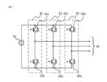
- FIG. 1 is a configuration diagram showing a power converter according to Embodiment 1;
- FIG. 3 is a diagram for explaining common mode noise that occurs in the power conversion system according to Embodiment 1;
- FIG. 1 is a configuration diagram showing a noise filter according to Embodiment 1;
- FIG. 2 is a configuration diagram showing a noise detection unit according to Embodiment 1;
- FIG. 2 is a configuration diagram showing an example of an amplifier according to Embodiment 1;
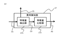
- FIG. 3 is a configuration diagram showing an example of an abnormality detection unit according to Embodiment 1;
- FIG. 4 is a configuration diagram showing an example of a feature amount detection unit according to Embodiment 1;
- FIG. 4 is a configuration diagram showing an example of a feature quantity comparison unit according to Embodiment 1;
- FIG. 2 is a configuration diagram showing an injection section according to Embodiment 1.
- FIG. FIG. 4 is a schematic diagram showing control response of the main circuit section of the noise filter according to Embodiment 1, and is a schematic diagram showing control response when there is no filter section.
- 4 is a schematic diagram showing pass characteristics of a filter unit according to Embodiment 1.
- FIG. FIG. 4 is a schematic diagram showing control response of the main circuit section of the noise filter according to Embodiment 1, and is a schematic diagram showing control response when there is a filter section.
- FIG. 4 is a schematic diagram showing a control response of the noise filter in Embodiment 1, and a schematic diagram showing a gain characteristic;
- FIG. 4 is a schematic diagram showing a control response of the noise filter in Embodiment 1, and a schematic diagram showing phase characteristics
- FIG. 4 is a schematic diagram showing the control response of the noise filter in Embodiment 1 when the control characteristic is changed due to the occurrence of an abnormality, and is a schematic diagram showing the change in the gain characteristic
- FIG. 4 is a schematic diagram showing the control response of the noise filter in Embodiment 1 when the control characteristic is changed due to the occurrence of an abnormality, and is a schematic diagram showing the change in the phase characteristic
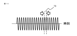
- 5 is a schematic diagram showing an abnormal output waveform of the cancel signal output section according to Embodiment 1
- FIG. FIG. 3 is a schematic diagram showing waveforms of common mode voltages in a normal state
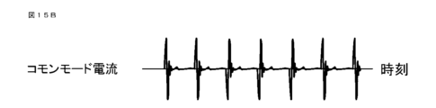
- FIG. 4 is a schematic diagram showing a waveform of common mode current in normal state;
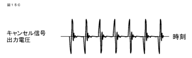
- FIG. 4 is a schematic diagram showing the waveform of the output voltage of the cancel signal according to Embodiment 1 at normal time;
- FIG. 4 is a schematic diagram showing a waveform of an output current of a cancel signal according to Embodiment 1 during normal operation;
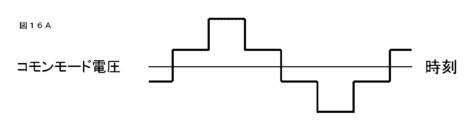
- FIG. 4 is a schematic diagram showing waveforms of common mode voltages in the event of an abnormality;
- FIG. 4 is a schematic diagram showing waveforms of common mode currents at the time of abnormality;
- FIG. 4 is a schematic diagram showing the waveform of the output voltage of the cancel signal according to Embodiment 1 at the time of abnormality;
- FIG. 4 is a schematic diagram showing a waveform of an output current of a cancel signal according to Embodiment 1 at the time of abnormality;
- FIG. 8 is a configuration diagram showing a feature amount detection unit according to another form of Embodiment 1;
- FIG. 10 is a configuration diagram of a noise filter according to Embodiment 2;
- FIG. 11 is a configuration diagram of a noise filter according to Embodiment 3;
- FIG. 11 is a configuration diagram of a feature amount detection unit according to Embodiment 4;
- FIG. 1 is a configuration diagram showing a power conversion system according to Embodiment 1
- FIG. 2 is a configuration diagram showing a power conversion device according to Embodiment 1.
- the power conversion system 100 is arranged between an AC power source 1 and a load 90, and includes a power conversion device 80 that converts input power from the AC power source 1 into arbitrary DC power or AC power, the AC power source 1, and the power conversion device.
- AC power supply 1 including noise filter 10 inserted between AC power supply 1 , noise filter 10 , power converter 80 , and load 90 are connected by electric line 11 .
- the electric circuit 11 is connected to a power line 2 (not shown) of the AC power supply 1 , and input power from the AC power supply 1 is input to the power converter 80 via the power line 2 .
- the power conversion device 80 converts the power input from the AC power supply 1 into the power required to drive the load 90 and outputs the power.
- noise filter 10 is arranged between AC power supply 1 and power conversion device 80 in Embodiment 1, noise filter 10 may be arranged between power conversion device 80 and load 90 .
- the power converter 80 is a two-level three-phase inverter, as shown in FIG. That is, two semiconductor switches 82a and 82b connected in series form one upper and lower arm 82.
- FIG. One upper and lower arm 83 is composed of two semiconductor switches 83a and 83b connected in series. Further, two semiconductor switches 84a and 84b connected in series form one upper and lower arm 84.
- a DC power supply 81 is connected to these three upper and lower arms 82 , 83 , 84 .
- the DC power supply 81 is configured by a converter or the like that converts the AC power input from the AC power supply 1 into DC power.
- An inverter output terminal 85 is connected to the midpoint of the three upper and lower arms 82 , 83 , 84 .
- These six semiconductor switches 82 a , 82 b , 83 a , 83 b , 84 a , 84 b perform switching operations to output AC power to the inverter output terminal 85 .
- the output potential of inverter output terminal 85 becomes either one of the positive voltage and the negative voltage of DC power supply 81 . Therefore, the common mode voltage of the power conversion device 80 becomes a constant voltage that is not zero.
- FIG. 3 is a diagram for explaining common mode noise generated in the power conversion system according to Embodiment 1, and shows a common mode equivalent circuit.
- the AC power supply 1 and the load 90 are connected on the ground side by the ground line 3 separately from the electric line 11 described above.
- the noise filter 10 is provided with a ground capacitor 15 having one end connected to the ground line 3 .
- a parasitic capacitance 86 and a parasitic capacitance 91 exist between the power converter 80 and the ground line 3 and between the load 90 and the ground line 3, respectively.
- the common mode voltage of the power converter 80 is applied to the common mode loop via the parasitic capacitances 86, 91 and the ground line 3, and the common mode current (common mode noise CN ) flows.
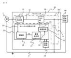
- FIG. 4 is a configuration diagram showing a noise filter according to Embodiment 1.
- FIG. Noise filter 10 is inserted between AC power supply 1 and power converter 80 .
- the noise filter 10 cancels from the noise detection unit 12 provided in the electric circuit 11 connected to the power supply line 2 (not shown) and the common mode noise CN (not shown in FIG. 4) detected by the noise detection unit 12.
- a control power source 19 that supplies power for generating and injecting the cancel signal CS to the cancel signal output unit 13 , and is inserted between the control power source 19 and the cancel signal output unit 13 .
- a protection circuit 18 capable of cutting off the supply of power from the control power supply 19 .
- a power supply cutoff means for cutting off the power supply to the amplifier 16 of the cancel signal output unit 13 is provided. It is.
- the protection circuit 18 is provided as one form of the power supply interrupting means.
- the cancel signal output unit 13 includes an amplifier unit 16 that amplifies the noise detection signal DS output from the noise detection unit 12, that is, a cancel signal generation unit, and sends the output from the amplifier unit 16 to the injection unit 14 as a cancel signal CS. , an abnormality detection section 17 capable of outputting an abnormality detection signal AS based on the output voltage of the amplification section 16 .
- the abnormality detection section 17 is composed of elements and circuits that hardly affect the output characteristics, and the output of the amplification section 16 is substantially the same as the cancel signal CS. Therefore, hereinafter, unless otherwise specified, the output of the amplifier 16 will also be referred to as the cancel signal CS.
- a filter section capable of adjusting the characteristics of the cancellation signal CS may be provided between the noise detection section 12 and the amplification section 16 or between the amplification section 16 and the abnormality detection section 17. . If a filter section is provided between the noise detection section 12 and the amplification section 16, the amplification section 16 amplifies the noise detection signal DS adjusted by the filter section to generate the cancellation signal CS. Even in this case, the characteristics of the cancellation signal CS are adjusted through the adjustment of the noise detection signal DS.
- the filter section an input filter circuit that adjusts the attenuation characteristics of the noise filter 10, such as reducing the gain of a specific band, is conceivable. It is conceivable to use an analog filter such as
- the noise filter 10 is provided with a grounding capacitor 15 connected between the electric circuit 11 and the grounding line 3 .
- the noise detection section 12 , the injection section 14 and the grounded capacitor 15 constitute the main circuit section 101 of the noise filter 10 .
- the control characteristics of the noise filter 10 greatly depend on the main circuit section 101 .
- the inductance value of the main circuit section 101 is the sum of the inductance value of the common mode transformer that constitutes the noise detection section 12 and the inductance value of the common mode transformer that constitutes the injection section 14 .
- the capacitance value of the main circuit section 101 is the capacitance value of the grounded capacitor 15 . Details of the control characteristics of the main circuit section 101 will be described later.
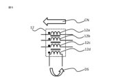
- FIG. 5 is a configuration diagram showing a noise detection unit according to Embodiment 1.
- the noise detection section 12 is composed of a common mode transformer.
- a common mode transformer that constitutes the noise detection unit 12 is referred to as a detection transformer here.
- This detection transformer has an R-phase winding 12a wound on an R-phase power line and an S-phase winding 12b wound on an S-phase power line in an electric circuit 11 connected to a power line 2 (not shown) of an AC power supply 1. , a T-phase winding 12c wound on the T-phase power line, and an auxiliary winding 12d.
- R-phase winding 12a, S-phase winding 12b, and T-phase winding 12c are wound in the same phase.
- noise detection unit 12 configured in this way, the magnetic fluxes generated in the normal mode cancel each other out, and the magnetic fluxes generated in the common mode strengthen each other.
- a detection transformer constructed in this way has a high inductance value only for common mode noise and acts as a common mode choke coil.
- noise detection signal DS is generated across the auxiliary winding 12d by common mode noise CN passing through the detection transformer. Both ends of the auxiliary winding 12 d are connected to the amplifying section 16 , and the noise detection signal DS is sent to the amplifying section 16 .
- FIG. 6 is a configuration diagram showing an example of an amplifier according to Embodiment 1.
- the amplifier section 16 includes an input resistor 16a, an operational amplifier 16b, and a feedback resistor 16c.
- the inverting input terminal of the operational amplifier 16b is connected to the input terminal side (left side in FIG. 6) of the amplifier section 16 via the input resistor 16a. 16b is connected to the output terminal. A non-inverting input terminal of the operational amplifier 16b is grounded.
- the amplifier 16 shown in FIG. 6 is an inverting amplifier circuit using an operational amplifier 16b, it may be a non-inverting amplifier circuit.
- the amplifying section 16 amplifies the noise detection signal DS with an amplification factor given by the ratio of the resistance value of the input resistor 16a to the resistance value of the feedback resistor 16c, generates the cancel signal CS, and outputs the cancel signal CS.
- FIG. 7 is a configuration diagram showing an example of an anomaly detection unit according to Embodiment 1.
- the abnormality detection unit 17 includes a feature amount detection unit 171 that outputs a feature amount signal CV for detecting an abnormality using the output voltage of the cancel signal CS, that is, a feature amount acquisition unit, and a predetermined value for the feature amount signal CV. It is composed of a feature amount comparison unit 172 that generates and outputs an abnormality detection signal AS by performing the calculated operation, that is, an abnormality determination unit.
- the abnormality detection signal AS is output when an abnormality of the noise filter 10 is detected, and is output when an abnormality is not detected.
- FIG. 8 is a configuration diagram showing an example of the feature amount detection unit according to Embodiment 1.
- the feature amount detection unit 171 generates and outputs a feature amount signal CV based on the voltage value of the output voltage of the cancel signal CS.
- the feature quantity signal CV is a signal representing a feature quantity used for abnormality detection.
- the feature amount detection unit 171 includes a capacitor 171k and a capacitor 171k and a It is configured by connecting a low-pass filter composed of a resistor 171m.
- the input terminal (not shown) of the feature amount detection section 171 is connected to the output terminal of the amplification section 16, and the output voltage of the cancel signal CS is input to the feature amount detection section 171 as an input signal.
- the input signal (cancellation signal CS) input to the feature amount detection unit 171 is sent to the injection unit 14 as shown in FIG. 8 and input to the absolute value detection circuit.
- the absolute value of the voltage value of the output voltage of the cancellation signal CS is output from the absolute value detection circuit. Since the output of the absolute value detection circuit is averaged by the low-pass filter, the low-pass filter outputs the voltage average value of the output voltage of the cancel signal CS.
- the output of the feature amount detection unit 171 indicates the voltage average value of the output voltage of the cancel signal CS. Become.
- the output of the feature amount detection section 171 is sent to the feature amount comparison section 172 as a feature amount signal CV.
- the circuit of the feature amount detection unit 171 is not limited to the example shown in FIG. 8, and can be freely configured without departing from the gist of the present application.
- FIG. 9 is a configuration diagram showing an example of a feature comparison unit according to Embodiment 1.
- the feature quantity comparison unit 172 generates an abnormality detection signal AS by performing a predetermined calculation on the feature quantity signal CV output by the feature quantity detection unit 171, and outputs the generated abnormality detection signal AS.
- the feature quantity comparison unit 172 is configured with a comparator circuit that compares the feature quantity signal CV with a predetermined threshold value.
- the feature amount comparison unit 172 includes a comparator 172a, a DC voltage source 172b, and a pull-up resistor 172c.
- the inverting input terminal of the comparator 172a is connected to the input terminal side (the left side in FIG.
- the non-inverting input terminal of the comparator 172a is connected to the positive terminal of the DC voltage source 172b.
- the negative electrode of the DC voltage source 172b is grounded.
- the output terminal of the comparator 172a is connected to the output terminal side (left side in FIG. 9) of the feature amount comparison section 172, and a pull-up resistor is provided between the output terminal of the comparator 172a and the output terminal of the feature amount comparison section 172. 172c is connected.
- the feature amount signal CV When the feature amount signal CV is input to the feature amount comparison unit 172 as an input signal, the magnitude of the feature amount signal CV is compared with the magnitude of the voltage of the DC voltage source 172b, and the abnormality detection signal AS is generated according to the comparison result. output. Specifically, for example, when the feature value signal CV is higher than the voltage of the DC voltage source 172b, the abnormality detection signal AS is output as an abnormality detection. In this case, the voltage value of the DC voltage source 172b serves as the threshold for determining whether there is an abnormality. Note that the circuit of the feature quantity comparison unit 172 is not limited to the example shown in FIG. 9, and can be freely configured within the scope of the present application.
- FIG. 10 is a configuration diagram showing an injection section according to Embodiment 1.
- the injection section 14 is composed of a common mode transformer.
- a common mode transformer that constitutes the injection section 14 is referred to as an injection transformer here.
- the injection transformer includes an R-phase winding 14a wound on the R-phase power line, an S-phase winding 14b wound on the S-phase power line, and a T-phase winding wound on the T-phase power line. It comprises a line 14c and an auxiliary winding 14d.
- the R-phase winding 14a, the S-phase winding 14b, and the T-phase winding 14c are wound in the same phase.
- An injection transformer constructed in this way has a high inductance value only for the common mode and acts as a common mode choke coil.
- the cancellation signal CS input to the auxiliary winding 14d causes the R-phase winding 14a to , S-phase winding 14b, and T-phase winding 14c, a voltage V that cancels common mode noise CN is induced.
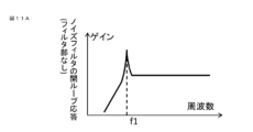
- FIG. 11A to 11C are schematic diagrams showing the control response of the main circuit section of the noise filter according to Embodiment 1.
- FIG. 11A is a schematic diagram showing the control response when there is no filter section
- FIG. FIG. 11C is a schematic diagram showing a pass characteristic
- FIG. 11C is a schematic diagram showing a control response when there is a filter section.
- the horizontal axis is frequency and the vertical axis is gain.
- the control response represents an open-loop response in a path starting from the output of the noise detection section 12 and fed back to the noise detection section 12 via the cancel signal output section 13 and the injection section 14 .
- the control stability of the noise filter 10 depends on the values of the gain margin and phase margin of the open loop response.
- the "filter section” is a filter section that adjusts the characteristics of the cancellation signal CS as described above, and the "filter section” in FIGS. means a filter section that is As described above, this filter section adjusts the characteristics of the cancellation signal CS through adjustment of the noise detection signal DS.
- a filter section having the filter pass characteristic shown in FIG. This filter section is configured such that its reject frequency coincides with the resonance frequency f1 of the main circuit section 101 .
- Such a filter section can be realized by a notch filter.
- the filter section when the filter section is provided between the noise detection section 12 and the amplification section 16, even if the common mode noise CN detected by the noise detection section 12 contains a component of the resonance frequency f1, the resonance peak can be generated by attenuating the cancellation signal CS. As a result, the noise filter 10 can exhibit a stable noise suppression effect.
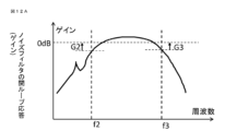
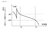
- FIGS. 12A and 12B are schematic diagrams showing the control response of the noise filter according to Embodiment 1.
- FIG. 12A is a schematic diagram showing gain characteristics
- FIG. 12B is a schematic diagram showing phase characteristics.
- the control response characteristic (control characteristic) of the noise filter 10 the phase rotates due to the phase delays of the main circuit section 101, the amplifier section 16, and the filter section.
- a notch filter and a low-pass filter are combined as a filter unit to suppress the resonance peak at the resonance frequency f1 as described above, and at the phase inversion frequency f2 in the low frequency band.
- the gain margin G2 and the gain margin G3 at the phase inversion frequency f3 in the high frequency band are set to values that can ensure control stability.
- the gain margins G2 and G3 are indicated by upward arrows when they have positive values, and are indicated by downward arrows when they have negative values.
- the value that can ensure control stability is, for example, 6 dB.
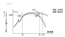
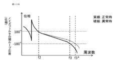
- FIG. 13A and 13B are schematic diagrams showing the control response of the noise filter in Embodiment 1.
- FIG. 13A is a schematic diagram showing changes in gain characteristics
- FIG. 13B is a schematic diagram showing changes in phase characteristics.
- 13A and 13B are diagrams showing the case where the control characteristics are changed due to the occurrence of an abnormality.
- the gain characteristics and phase characteristics during normal conditions are represented by solid lines
- the gain characteristics and phase characteristics during abnormal conditions are represented by dashed lines.
- an "abnormality” an example in which the high-frequency phase inversion frequency f3 fluctuates to the frequency f3* is shown.
- a typical example of such an anomaly is loss of the function of the low-pass filter due to a component failure or the like, which causes a change in the characteristics of the filter section.
- the value of the gain margin G3 at the phase inversion frequency f3 in the high frequency band fluctuates, and may deviate from the value at which control stability can be ensured.
- FIG. 14 is a schematic diagram showing an abnormal output waveform of the cancel signal output section according to Embodiment 1, and shows an example of the waveform of the cancel signal CS in an abnormal state.
- the horizontal axis is time.
- the frequency component of the phase inversion frequency f3 continues to be amplified as shown in FIG. 14, causing oscillation.
- the section sandwiched between the arrow and the dashed line indicates the period T3 of the cancel signal CS at the time of abnormality.
- the period T3 is equal to the reciprocal of the phase inversion frequency f3.
- the noise source of the common mode noise CN also occurs in the noise filter 10 in the common mode equivalent circuit shown in FIG.
- the load 90, system, and power converter 80 share the noise source voltage according to their impedance ratios.
- the noise filter 10 not operate normally and a normal amount of attenuation cannot be obtained, but also the conduction noise originating from the oscillation operation of the noise filter 10 itself flows out to the system via the electric circuit 11. also occur.
- the shaft voltage of the motor may be increased.
- the common mode noise CN generated by itself may cause a malfunction.
- the injection section 14 is configured by a common mode transformer. Since the common mode transformer constituting the injection section 14 serves as an inductance load having an inductive impedance for the cancel signal output section 13, the impedance is high in a high frequency range. Therefore, even if the cancel signal output unit 13 continues the abnormal high-frequency oscillation operation as shown in FIG. 14 and the noise filter 10 cannot perform normal noise suppression operation, However, phenomena such as overvoltage or overcurrent that affect the standards of circuit components do not occur immediately. This means that even if the noise filter 10 is provided with an overvoltage protection circuit or an overcurrent protection circuit, the noise filter 10 will not be stopped by the protection function as long as the abnormality of the noise filter 10 cannot be detected. do.
- the noise filter 10 performs abnormality detection by the abnormality detection unit 17, and when an abnormality is detected, operates the protection circuit 18 to stop generation and injection of the cancel signal CS.
- the protection circuit 18 to stop generation and injection of the cancel signal CS.
- FIG. 15A is a schematic diagram showing the waveform of the common mode voltage during normal operation
- FIG. 15B is a schematic diagram showing the waveform of the common mode current
- FIG. 15C is a schematic diagram showing the waveform of the output voltage of the cancel signal according to Embodiment 1 in the normal state
- FIG. 15D is a schematic diagram showing the waveform of the output current of the cancel signal.
- the horizontal axis is time.
- the common mode voltage is the voltage of common mode noise CN.
- the common mode current is the current that flows through the electric circuit 11 due to the common mode voltage. When the common mode voltage is input to the common mode equivalent circuit shown in FIG. It is the current that flows through the electric circuit 11 .
- the common mode voltage is generated with the switching operation of each semiconductor switch of the power converter 80 shown in FIG. 2, and has a rectangular waveform as shown in FIG. 15A. Common mode currents have a spike-like waveform as shown in FIG. 15B and cause noise problems at various points along the path.
- the noise detection section 12 of the noise filter 10 detects the common mode current and sends the noise detection signal DS to the cancellation signal output section 13, and the cancellation signal output section 13 generates the cancellation signal CS from the noise detection signal DS.
- the cancel signal CS is injected into the electric path 11 via the injection section 14 .
- the output voltage of the cancel signal CS in normal times has a spike-like waveform as shown in FIG. 15C.
- the output current of the cancel signal CS caused by the output voltage of the cancel signal CS also has a spike-like waveform as shown in FIG. 16D. Since the output current of the cancel signal CS is a current that cancels out the common mode current, it has a characteristic that it has a waveform whose average value and effective value are extremely smaller than the peak value, like the common mode current.
- the noise current flowing out of the power conversion device 80 which is the noise source of the common mode noise CN, passes through the injection unit 14, so that a disturbance component is superimposed on the output current of the cancellation signal CS, and the cancellation A disturbance component is also superimposed on the output voltage of the cancel signal CS due to the product of the output impedance of the signal CS and the current.
- superimposition as described above is ignored in FIGS. 15C and 15D.
- FIG. 16A is a schematic diagram showing the waveform of common mode voltage in the event of an abnormality
- FIG. 16B is a schematic diagram showing the waveform of common mode current
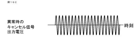
- FIG. 16C is a schematic diagram showing the waveform of the output voltage of the cancel signal according to Embodiment 1
- FIG. 16D is a schematic diagram showing the waveform of the output current of the cancel signal at the time of abnormality.
- the horizontal axis is time.
- the common mode voltage and common mode current do not change even in the event of an abnormality.
- the control characteristic of the noise filter 10 changes, causing the cancellation signal CS to oscillate. Therefore, as shown in FIGS.
- the waveforms of the output voltage and output current of the cancel signal CS are abnormal output waveforms as shown in FIG.
- the abnormal output waveform does not have the characteristics of the normal waveform, that is, the average value and the effective value are extremely smaller than the peak value.
- the voltage average value of the output voltage of the cancel signal CS is 2/ ⁇ times the voltage peak value, and there is no large difference between the peak value and the average value.
- the current average value of the output current of the cancel signal CS is 2/ ⁇ times the current peak value, and there is no large difference between the peak value and the average value. This is the same even if the output voltage of the operational amplifier saturates due to the high-gain oscillation operation and the waveform of the output voltage of the cancel signal CS becomes rectangular.
- the effective values of the output voltage and output current are also 1/ ⁇ 2 times the peak value, so the relationship between the peak value and the effective value is the same as the relationship between the peak value and the average value described above. is. However, the following description focuses on the average value.
- the average voltage value of the output voltage of the cancel signal CS and the average current value of the output current of the cancel signal CS are larger in the abnormal state than in the normal state. That is, in this case, the voltage average value of the output voltage of the cancel signal CS can be used as the criterion.
- the noise filter 10 is operating normally, that is, whether the noise filter 10 can cancel the common mode current. It is possible to determine whether there is an abnormal operation for some reason.
- V1 is the voltage average value of the output voltage of the cancel signal CS in the normal state
- Vth is the threshold value of the voltage average value for determining the presence or absence of an abnormality
- V2 is the voltage average value in the abnormal operation.
- the feature amount detection unit 171 outputs the voltage average value of the output voltage of the cancel signal CS as the feature amount signal CV. Furthermore, the output voltage value of the DC voltage source 172b of the feature quantity comparison unit 172 serves as a threshold value for determining the presence or absence of abnormality. That is, the output voltage value of the DC voltage source 172b is the threshold value Vth of the voltage average value. As a result, the feature quantity comparison unit compares the voltage average value of the output voltage of the cancel signal CS with the threshold value Vth of the voltage average value. When the voltage average value of the output voltage of the cancel signal CS exceeds the threshold value Vth, the output of the comparator 172a becomes high, and the feature quantity comparison section 172 outputs the abnormality detection signal AS. When the voltage average value of the output voltage of the cancel signal CS is equal to or less than the threshold value Vth, the output of the comparator 172a becomes low, and the feature quantity comparison section 172 outputs the abnormality detection signal AS off.
- the abnormality detection signal AS output from the feature quantity comparison unit 172 is input to the protection circuit 18 .
- the protection circuit 18 typically consists of a control relay.
- the protection circuit 18 disconnects the control power source 19 and the cancel signal output unit 13 based on the abnormality detection signal AS, and cuts off the power supply from the control power source 19 to the cancel signal output unit 13 .
- the cancellation signal CS is not generated by the amplification section 16 in the cancellation signal output section 13 to which the power supply is stopped.
- injection of the cancel signal CS into the electric line 11 is also stopped, so injection of the cancel signal CS having an abnormal output waveform into the electric line 11 is prevented.
- the abnormality detection unit 17 After the abnormality detection unit 17 detects an abnormality and causes the protection circuit 18 to perform the blocking operation, for example, when the feature amount comparison unit 172 outputs the abnormality detection signal AS in an OFF state, the protection circuit 18 performs the blocking operation. is reset to resume the generation and injection of the cancel signal CS.
- the protection circuit 18 For abnormalities that are known to be temporary, it is conceivable to use a delay circuit or a counter circuit to restore the system after a preset period of time has elapsed.
- an example of a circuit using the operational amplifier 16b is shown as the configuration of the amplifier section 16.
- the configuration of the amplifier section 16 for example, other inverting amplifier circuit or non-inverting amplifier circuit may be used. good.
- the protection circuit 18 has shown an example in which it cuts off in response to the abnormality detection signal AS. Combinations may allow operations other than simple blocking operations.
- an example of a circuit using an operational amplifier has been shown as the configuration of the feature amount detection unit 171, a circuit that achieves the same purpose, for example, may be used.
- the feature amount detection unit 171 may be configured to detect different values such as an instantaneous value and an effective value as the feature amount. Also, although an example of a circuit using the comparator 172a as the configuration of the feature quantity comparison unit 172 has been shown, another circuit that achieves the same purpose, for example, may be used.
- noise filter 10 of Embodiment 1 other common mode choke coils may be connected on the electric path 11 in addition to the noise detection section 12 and the injection section 14 .
- one or both of the noise detection section 12 and the injection section 14 may be configured using a capacitor instead of the common mode transformer.
- the injection section 14 is composed of a capacitor, a pulse transformer may be inserted between the injection section 14 and the cancel signal output section 13 .
- the injection unit 14 when the injection unit 14 is configured using a capacitor instead of the common mode transformer and no pulse transformer is inserted between the capacitor and the cancel signal output unit 13, the cancel signal output For section 13, the impedance of injection section 14 will be capacitive. In this case, the frequency band in which abnormality detection is difficult without the abnormality detection unit 17 is the low frequency band.
- the injection section 14 when the injection section 14 is configured using a capacitor instead of the common mode transformer and a pulse transformer is inserted between the capacitor and the cancel signal output section 13, the injection section 14 is The impedance of becomes inductive, and similarly to the case where the injection section 14 is configured by a common mode transformer, the frequency band in which abnormality detection is difficult without the abnormality detection section 17 is a high frequency band.
- the abnormality detection part 17 can perform reliable abnormality detection in the first embodiment. .
- the protection circuit 18 is used as one form of the power supply cutoff means, but as another form of the power supply cutoff means, a control circuit for stopping the control power supply 19 based on the abnormality detection signal AS is provided. can also be used.
- an abnormality detection unit detects an abnormality of the noise filter and outputs an abnormality detection signal, and based on the abnormality detection signal, cuts off the power supply to the cancel signal output unit. and a protection circuit that As a result, when an abnormality occurs due to a change in the control characteristics of the noise filter, the abnormality is detected from the change in the output voltage of the cancellation signal due to the abnormality, and by stopping the power supply to the cancellation signal output section, the abnormal cancellation signal is detected. can be prevented from being injected into the electric circuit, so it has high reliability. In particular, it has high reliability against changes in the control characteristics of the noise filter itself.
- the abnormality of the noise filter is detected based on the output voltage of the cancel signal, even if the injection part of the cancel signal is configured with an inductance load such as a common mode transformer, the abnormality of the noise filter in the high frequency band can be reliably detected. In addition, even if the injection section is composed of a capacitive load such as a capacitor, it is possible to reliably detect an abnormality of the noise filter in a low frequency band.
- FIG. 17 is a configuration diagram showing a feature amount detection unit according to another mode of Embodiment 1.
- the feature amount detection unit 1711 detects the current average value of the output current of the cancel signal CS as the feature amount.
- the feature amount detection section 1711 is provided with an absolute value detection circuit.
- a current detection resistor 171p such as a shunt resistor is arranged between the injection unit 14 and the control ground.
- the input signal of the absolute value detection circuit in the feature amount detection unit 1711 becomes the output current of the cancel signal CS.
- the feature value signal CV becomes the current average value of the cancel signal CS.
- Embodiment 2 is a configuration diagram of a noise filter according to Embodiment 2.
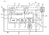
- FIG. 1 a protection circuit 28 is inserted between the abnormality detection section 17 and the injection section 14 in the cancel signal output section 23 .
- the anomaly detection unit 17 outputs an anomaly detection signal AS to the protection circuit 28 .
- the cancellation signal CS output from the amplification section 16 is sent to the injection section 14 through the abnormality detection section 17 and the protection circuit 18 .
- a protection means for suppressing the injection of the abnormal cancel signal CS into the electric line 11 an injection for blocking transmission of the cancel signal CS from the amplifier 16 of the cancel signal output unit 13 to the injection unit 14 is provided. It has blocking means.
- a protection circuit 28 is provided as one form of injection blocking means.
- the protection circuit 28 cuts off the path of the cancellation signal CS between the abnormality detection unit 17 and the injection unit 14 based on the abnormality detection signal AS. This prevents the abnormal cancel signal CS from being sent to the injection unit 14 when an abnormality is detected by the abnormality detection unit 17 , thereby preventing the injection of the abnormal cancel signal CS into the electric line 11 . escape.
- the configuration of the protection circuit 28 may be the same as that of the protection circuit 18 of the first embodiment. It should be noted that the second embodiment and the first embodiment may be combined to provide both the protection circuit 18 and the protection circuit 28 .
- Embodiment 3 is a configuration diagram of a noise filter according to Embodiment 3.
- FIG. Both of the noise filters of Embodiments 1 and 2 are equipped with a protection circuit that performs a cutoff operation in response to an abnormality detection signal AS.
- Embodiment 3 notifies the noise source of the abnormality of the noise filter instead of such a protection circuit.
- the noise filter 30 is provided with an abnormal state signal output section 38 in the cancel signal output section 33 , and the abnormality detection signal AS output by the abnormality detection section 17 is input to the abnormal state signal output section 38 .
- an abnormal state signal output section 38 is provided as protection means for suppressing injection of an abnormal cancel signal CS into the electric line 11 .
- the abnormal state signal output unit 38 has an output circuit capable of outputting a signal to the power conversion device 80, and outputs an abnormal state signal AS2 to the power conversion device 80 when the abnormality detection signal AS is input.
- the abnormal state signal AS2 is typically a differential signal or a low-impedance current signal that is resistant to disturbance, and is created based on the abnormality detection signal AS.
- the abnormal state signal AS2 is isolated from the control potential of the noise filter 30 as required.
- the power conversion device 80 Upon receiving the abnormal state signal AS2, the power conversion device 80 recognizes that the noise filter 30 is in an abnormal state. After recognizing that the noise filter 30 is in an abnormal state, the power conversion device 80 takes measures such as stopping the operation according to the content of the abnormality.
- a control circuit for stopping power conversion device 80 based on abnormal state signal AS2 may be provided outside or inside power conversion device 80 . Such a control circuit receives the abnormal condition signal AS2 and sends a stop command to the power conversion device 80 if necessary.
- Embodiment 3 a highly reliable noise filter can be provided. Unlike Embodiments 1 and 2, Embodiment 3 does not directly prevent injection of an abnormal cancellation signal into an electrical path by a protection circuit. However, the abnormal state signal makes the power converter, which is the noise source of common mode noise, recognize the abnormality of the noise filter. In this case, the power converter takes measures such as stopping operation as necessary, so stopping the noise source of the common mode noise can prevent an abnormal cancellation signal from being generated and injected into the electric circuit. can. As described above, the third embodiment has high reliability by indirectly preventing an abnormal cancellation signal from being injected into the electric circuit by making the power conversion device, which is a noise source, recognize the abnormality of the noise filter. It is the realization of sexuality.
- the protective circuits of the first and second embodiments may be combined with the third embodiment. Further, in the third embodiment, since an abnormal state signal is output to a noise source of common mode noise, if there is another controlled device that is a noise source of common mode noise, may be configured to output an abnormal state signal also to the controlled device.
- Embodiment 4 differs from Embodiments 1 to 3 in the feature amount detection unit.
- 20 is a configuration diagram of a feature amount detection unit according to Embodiment 4.
- FIG. The feature amount detection unit 471 of the noise filter 40 (not shown) is obtained by adding a feature amount detection filter unit 471n, that is, a band-limiting filter unit to the feature amount detection unit 1711 shown in FIG. More specifically, a current detection resistor 171p is provided between the injection section 14 and the control ground.
- a feature amount detection filter unit 471n is provided on an electric path connecting the two sides.
- the input signal of the feature amount detection section 171 is the output current of the cancellation signal CS, as with the feature amount detection section 1711 .
- the feature amount detection filter section 471n is provided in the feature amount detection section 1711, but the feature amount detection filter section 471n may be provided in the feature amount detection section 171 shown in FIG.
- the feature amount detection filter unit 471n performs filtering processing on the input signal of the feature amount detection unit 471, and is configured to weight according to each frequency component, such as high frequencies above a certain frequency. It typically includes a low-pass filter, high-pass filter, notch filter, band-pass filter, or a filter circuit combining these. Note that the “weighting” here includes setting the weight of a specific frequency component to zero, that is, removing the specific frequency component. Therefore, the feature amount detection filter unit 471n can reliably detect a desired abnormality among various abnormalities that may occur in the noise filter 40 by removing disturbance components in advance. A specific description will be given below.
- the cancel signal CS has an abnormal output waveform as shown in FIG. 14 and the like.
- the noise current flowing out from the power conversion device 80 which is the noise source, passes through the injection unit 14, so that a disturbance component is superimposed on the output voltage and output current of the cancel signal CS.
- This disturbance component includes various frequency components, but in noise suppression by an active noise filter, it is necessary to limit the band targeted for noise suppression in order to avoid an increase in the power required for the control circuit of the active noise filter. Common.
- a band lower than 150 kHz, which is the noise standard target band is generally not actively suppressed. is generally outside the suppression band.
- the noise current of the frequency component near the switching carrier frequency of the power conversion device 80 may be flowed into the system without reducing the amplitude of the noise current in this band without performing noise suppression by the active noise filter. be.
- the resulting disturbance in the output voltage and output current of the cancellation signal may not be negligible.
- the feature amount detection filter unit 471n removes the frequency component near the switching carrier frequency as described above from the input signal of the feature amount detection unit 471 (the output voltage or the output current of the cancellation signal CS). can do. Thereby, the feature amount signal CV can be generated after removing the influence of the disturbance, and the abnormality can be detected. Therefore, according to the fourth embodiment, it is possible to reliably detect a desired abnormality.
- the feature amount detection filter section the feature amount is detected after weighting the cancellation signal according to each frequency component, so that the desired abnormality can be reliably detected.
- the noise filter of the present application is applied to a three-phase, three-wire power conversion system. may apply. For example, it may be applied to a three-phase four-wire power conversion system, or may be applied to a single-phase two-wire or single-phase three-wire power conversion system.
- the description is basically based on analog circuits, but it is also possible to apply them to digital circuits.
- the feature amount detection section of the abnormality detection section may perform spectrum analysis of the output voltage or output current of the cancel signal, and the abnormality detection may be performed based on the analysis result.
Landscapes
- Engineering & Computer Science (AREA)
- Power Engineering (AREA)
- Power Conversion In General (AREA)
Abstract
Description
このように、従来のアクティブノイズフィルタは、制御特性の変化に対して信頼性が十分でないという問題点があった。
まず、実施の形態1を図1から図16Dに基づいて説明する。
図1は、実施の形態1に係る電力変換システムを示す構成図であり、図2は、実施の形態1に係る電力変換装置を示す構成図である。電力変換システム100は、交流電源1と負荷90との間に配置され、交流電源1からの入力電力を任意の直流電力または交流電力に変換する電力変換装置80と、交流電源1と電力変換装置80との間に挿入されたノイズフィルタ10とを備える交流電源1、ノイズフィルタ10、電力変換装置80、および負荷90は、電路11により接続されている。電路11は、交流電源1の電源線2(図示無し)につながっており、交流電源1からの入力電力は、電源線2を介して電力変換装置80に入力される。電力変換装置80は、交流電源1から入力される電力を負荷90の駆動に必要な電力に変換して出力する。なお、実施の形態1において、ノイズフィルタ10は交流電源1と電力変換装置80との間に配置されているが、電力変換装置80と負荷90との間に配置されていてもよい。
次に、実施の形態2を図18に基づいて説明する。なお、図1から図17と同一または相当部分については同一符号を付し、その説明を省略する。図18は、実施の形態2におけるノイズフィルタの構成図である。ノイズフィルタ20は、キャンセル信号出力部23において、異常検知部17と注入部14との間に保護回路28が挿入されている。一方、実施の形態1のノイズフィルタ10において制御電源19とキャンセル信号出力部13との間に挿入されていた保護回路18は無い。異常検知部17は、異常検知信号ASを保護回路28に出力する。ノイズフィルタ20において、増幅部16から出力されたキャンセル信号CSは、異常検知部17および保護回路18を通って注入部14に送られる。実施の形態2では、異常なキャンセル信号CSが電路11に注入されることを抑制する保護手段として、キャンセル信号出力部13の増幅部16から注入部14へのキャンセル信号CSの送信を遮断する注入阻止手段を備えているものである。また、実施の形態2では注入阻止手段の一形態として、保護回路28を備える。
その他については実施の形態1と同様であるので、その説明を省略する。
次に、実施の形態3を図19に基づいて説明する。なお、図1から図18と同一または相当部分については同一符号を付し、その説明を省略する。図19は、実施の形態3におけるノイズフィルタの構成図である。実施の形態1および2のノイズフィルタは、いずれも異常検知信号ASによって遮断動作を行う保護回路を備えたものであった。実施の形態3は、このような保護回路の代わりに、ノイズフィルタの異常をノイズ源に通知する。ノイズフィルタ30は、キャンセル信号出力部33に異常状態信号出力部38が設けられており、異常検知部17が出力した異常検知信号ASは、異常状態信号出力部38に入力される。実施の形態3では、異常なキャンセル信号CSが電路11に注入されることを抑制する保護手段として、異常状態信号出力部38を備える。
次に、実施の形態4を図20に基づいて説明する。なお、図1から図19と同一または相当部分については同一符号を付し、その説明を省略する。実施の形態4は、特徴量検出部が実施の形態1から3と異なる。図20は、実施の形態4に係る特徴量検出部の構成図である。ノイズフィルタ40(図示無し)の特徴量検出部471は、図17で示した特徴量検出部1711に特徴量検出フィルタ部471n、すなわち帯域制限フィルタ部を設けたものである。より具体的には、注入部14と制御グラウンドとの間に電流検出抵抗171pが設けられ、抵抗171pの注入部14側の端子と注入部14とを接続する電路と、絶対値検波回路の入力側とを接続する電路に特徴量検出フィルタ部471nが設けられている。特徴量検出部171の入力信号は、特徴量検出部1711と同様に、キャンセル信号CSの出力電流となる。実施の形態4では特徴量検出部1711に特徴量検出フィルタ部471nを設ける構成となっているが、図8に示した特徴量検出部171に特徴量検出フィルタ部471nを設けてもよい。
また、特徴量検出フィルタ部を備えたことにより、キャンセル信号に対してそれぞれの周波数成分に応じた重み付けをした上で特徴量の検出を行うため、所望の異常の検知を確実に行うことができる。
従って、例示されていない無数の変形例が、本願に開示される技術の範囲内において想定される。例えば、少なくとも1つの構成要素を変形する場合、追加する場合または省略する場合、さらには、少なくとも1つの構成要素を抽出し、他の実施の形態の構成要素と組み合わせる場合が含まれるものとする。
例えば、本願で開示した各実施の形態では、三相三線式の電力変換システムに本願のノイズフィルタを適用する形態を示したが、相数、線数の異なる電力変換システムに本願のノイズフィルタを適用してもよい。例えば、三相四線式の電力変換システムに適用してもよいし、単相二線式、単相三線式の電力変換システムに適用することも考えられる。
また、上述した実施の形態1から4では、基本的にアナログ回路を前提に説明したが、デジタル回路に適用することも可能である。この場合、異常検知部の特徴量検出部においてキャンセル信号の出力電圧または出力電流のスペクトル分析を行い、その結果に基づいて異常検知をしてもよい。
Claims (9)
- 交流電源と、前記交流電源から電力の供給を受ける負荷と、前記交流電源から出力された交流電力を変換し、変換した前記交流電力を前記負荷に出力する電力変換装置とを接続する電路に設けられたノイズフィルタであって、
前記電路を流れるコモンモードノイズを検出するノイズ検出部と、
前記ノイズ検出部が検出した前記コモンモードノイズに基づいて、前記コモンモードノイズを相殺するキャンセル信号を生成するキャンセル信号生成部と、
前記キャンセル信号を前記電路に注入する注入部と、
前記キャンセル信号の出力電圧または出力電流に基づいて前記ノイズフィルタの異常を検知し、異常検知信号を出力する異常検知部と、
前記異常検知信号に基づいて、異常な前記キャンセル信号が前記電路に注入されることを抑制する保護手段と
を備えたことを特徴とするノイズフィルタ。 - 前記保護手段は、前記キャンセル信号生成部への電力供給を遮断する電力供給遮断手段を備えている請求項1に記載のノイズフィルタ。
- 前記電力供給遮断手段は、前記キャンセル信号生成部に電力を供給する制御電源と前記キャンセル信号生成部との接続を切り離す保護回路を備えている請求項2に記載のノイズフィルタ。
- 前記保護手段は、前記キャンセル信号生成部から前記注入部への前記キャンセル信号の送信を遮断する注入阻止手段を備えている請求項1から3のいずれか1項に記載のノイズフィルタ。
- 前記注入阻止手段は、前記キャンセル信号生成部と前記注入部との接続を切り離す第2の保護回路を備えている請求項4に記載のノイズフィルタ。
- 前記保護手段は、前記ノイズフィルタに異常が発生していることを示す異常状態信号を前記異常検知信号に基づいて生成し、前記コモンモードノイズのノイズ源となっている被制御機器に対して前記異常状態信号を出力する異常状態信号出力部を備えている請求項1から5のいずれか1項に記載のノイズフィルタ。
- 前記異常検知部は、前記キャンセル信号の出力電圧または出力電流に基づく特徴量を取得する特徴量取得部と、前記特徴量の大きさに基づいて異常の有無の判定をし、前記判定の結果に基づいて前記異常検知信号を出力する異常判定部を備えている請求項1から6のいずれか1項に記載のノイズフィルタ。
- 前記特徴量取得部は、前記キャンセル信号に含まれるそれぞれの周波数成分に対し、前記それぞれの周波数成分に応じた重み付けをする帯域制限フィルタ部を備え、前記特徴量取得部は、前記重み付けをされた前記キャンセル信号の出力電圧または出力電流に基づいて、前記特徴量を検出する請求項7に記載のノイズフィルタ。
- 前記特徴量は、前記キャンセル信号の出力電圧または出力電流の実効値、平均値、または瞬時値である請求項7または8に記載のノイズフィルタ。
Priority Applications (3)
| Application Number | Priority Date | Filing Date | Title |
|---|---|---|---|
| EP21967185.6A EP4447317A4 (en) | 2021-12-08 | 2021-12-08 | NOISE FILTER |
| JP2023565781A JP7738675B2 (ja) | 2021-12-08 | 2021-12-08 | ノイズフィルタ |
| PCT/JP2021/045157 WO2023105687A1 (ja) | 2021-12-08 | 2021-12-08 | ノイズフィルタ |
Applications Claiming Priority (1)
| Application Number | Priority Date | Filing Date | Title |
|---|---|---|---|
| PCT/JP2021/045157 WO2023105687A1 (ja) | 2021-12-08 | 2021-12-08 | ノイズフィルタ |
Publications (1)
| Publication Number | Publication Date |
|---|---|
| WO2023105687A1 true WO2023105687A1 (ja) | 2023-06-15 |
Family
ID=86729936
Family Applications (1)
| Application Number | Title | Priority Date | Filing Date |
|---|---|---|---|
| PCT/JP2021/045157 Ceased WO2023105687A1 (ja) | 2021-12-08 | 2021-12-08 | ノイズフィルタ |
Country Status (3)
| Country | Link |
|---|---|
| EP (1) | EP4447317A4 (ja) |
| JP (1) | JP7738675B2 (ja) |
| WO (1) | WO2023105687A1 (ja) |
Cited By (2)
| Publication number | Priority date | Publication date | Assignee | Title |
|---|---|---|---|---|
| CN120016819A (zh) * | 2025-04-22 | 2025-05-16 | 西安交通大学 | 一种基于方波解析重构的数字有源emi滤波方法及电路 |
| WO2025175727A1 (zh) * | 2024-02-19 | 2025-08-28 | 华为数字能源技术有限公司 | 一种功率变换器和光伏发电系统 |
Citations (5)
| Publication number | Priority date | Publication date | Assignee | Title |
|---|---|---|---|---|
| JP2010057268A (ja) | 2008-08-28 | 2010-03-11 | Fuji Electric Systems Co Ltd | 伝導性ノイズフィルタ |
| WO2012137258A1 (ja) * | 2011-04-08 | 2012-10-11 | 三菱電機株式会社 | 電力変換装置、モータ駆動装置および冷凍空気調和装置 |
| WO2021166018A1 (ja) * | 2020-02-17 | 2021-08-26 | 三菱電機株式会社 | ノイズ抑制装置 |
| WO2021166397A1 (ja) * | 2020-02-18 | 2021-08-26 | オムロン株式会社 | ノイズフィルタ |
| WO2021234760A1 (ja) * | 2020-05-18 | 2021-11-25 | 三菱電機株式会社 | 電力変換装置 |
Family Cites Families (4)
| Publication number | Priority date | Publication date | Assignee | Title |
|---|---|---|---|---|
| JP2007282313A (ja) * | 2006-04-03 | 2007-10-25 | Denso Corp | 回転機駆動装置 |
| EP2709250A1 (en) * | 2012-09-13 | 2014-03-19 | Nxp B.V. | Noise filtering |
| JP7396043B2 (ja) * | 2019-12-27 | 2023-12-12 | オムロン株式会社 | ノイズフィルタ装置及び電力システム |
| WO2021192042A1 (ja) * | 2020-03-24 | 2021-09-30 | 三菱電機株式会社 | ノイズ低減装置 |
-
2021
- 2021-12-08 WO PCT/JP2021/045157 patent/WO2023105687A1/ja not_active Ceased
- 2021-12-08 EP EP21967185.6A patent/EP4447317A4/en active Pending
- 2021-12-08 JP JP2023565781A patent/JP7738675B2/ja active Active
Patent Citations (5)
| Publication number | Priority date | Publication date | Assignee | Title |
|---|---|---|---|---|
| JP2010057268A (ja) | 2008-08-28 | 2010-03-11 | Fuji Electric Systems Co Ltd | 伝導性ノイズフィルタ |
| WO2012137258A1 (ja) * | 2011-04-08 | 2012-10-11 | 三菱電機株式会社 | 電力変換装置、モータ駆動装置および冷凍空気調和装置 |
| WO2021166018A1 (ja) * | 2020-02-17 | 2021-08-26 | 三菱電機株式会社 | ノイズ抑制装置 |
| WO2021166397A1 (ja) * | 2020-02-18 | 2021-08-26 | オムロン株式会社 | ノイズフィルタ |
| WO2021234760A1 (ja) * | 2020-05-18 | 2021-11-25 | 三菱電機株式会社 | 電力変換装置 |
Non-Patent Citations (1)
| Title |
|---|
| See also references of EP4447317A4 |
Cited By (2)
| Publication number | Priority date | Publication date | Assignee | Title |
|---|---|---|---|---|
| WO2025175727A1 (zh) * | 2024-02-19 | 2025-08-28 | 华为数字能源技术有限公司 | 一种功率变换器和光伏发电系统 |
| CN120016819A (zh) * | 2025-04-22 | 2025-05-16 | 西安交通大学 | 一种基于方波解析重构的数字有源emi滤波方法及电路 |
Also Published As
| Publication number | Publication date |
|---|---|
| JPWO2023105687A1 (ja) | 2023-06-15 |
| EP4447317A4 (en) | 2025-01-29 |
| JP7738675B2 (ja) | 2025-09-12 |
| EP4447317A1 (en) | 2024-10-16 |
Similar Documents
| Publication | Publication Date | Title |
|---|---|---|
| CA2221803C (en) | Transformerless conditioning of a power distribution system | |
| US6025980A (en) | Earth leakage protective relay | |
| US20030197989A1 (en) | Method and apparatus for high impedance grounding of medium voltage AC drives | |
| US7659797B2 (en) | Low-leakage EMC filter | |
| US10069480B2 (en) | Active filter device and circuit arrangement comprising an active filter device | |
| WO2014048471A1 (en) | Power line filter device | |
| US9013840B2 (en) | Adaptive line filter | |
| JP7738675B2 (ja) | ノイズフィルタ | |
| JPWO2013111360A1 (ja) | 高周波電流低減装置 | |
| US11843384B2 (en) | Noise reduction device | |
| WO2018109801A1 (ja) | 電力変換装置 | |
| US11990833B2 (en) | Noise filter | |
| EP1236260A1 (en) | A three stage power conditioning circuit | |
| JPWO2023105687A5 (ja) | ||
| US20210006235A1 (en) | Compensation Filter and Method for Activating a Compensation Filter | |
| JP7814542B2 (ja) | ノイズフィルタ、電力変換システム及び管理システム | |
| JPH04271225A (ja) | 漏電保護システムと漏電遮断器 | |
| US20230163681A1 (en) | Electromagnetic interference suppression circuit | |
| JP4715537B2 (ja) | 漏電遮断器 | |
| KR102551607B1 (ko) | 누전 차단기 | |
| CN113196636B (zh) | 用于运行供电装置的方法以及供电装置 | |
| JP2021182480A (ja) | 漏電遮断器 | |
| JP2024053311A (ja) | 電流注入型アクティブフィルタ及び回路 | |
| JPH04172915A (ja) | 漏電遮断器 | |
| JPH08317561A (ja) | 高調波抑制装置 |
Legal Events
| Date | Code | Title | Description |
|---|---|---|---|
| 121 | Ep: the epo has been informed by wipo that ep was designated in this application |
Ref document number: 21967185 Country of ref document: EP Kind code of ref document: A1 |
|
| ENP | Entry into the national phase |
Ref document number: 2023565781 Country of ref document: JP Kind code of ref document: A |
|
| WWE | Wipo information: entry into national phase |
Ref document number: 18707884 Country of ref document: US |
|
| WWE | Wipo information: entry into national phase |
Ref document number: 2021967185 Country of ref document: EP |
|
| NENP | Non-entry into the national phase |
Ref country code: DE |
|
| ENP | Entry into the national phase |
Ref document number: 2021967185 Country of ref document: EP Effective date: 20240708 |