WO2023119833A1 - アンテナモジュールおよびその製造方法 - Google Patents
アンテナモジュールおよびその製造方法 Download PDFInfo
- Publication number
- WO2023119833A1 WO2023119833A1 PCT/JP2022/039252 JP2022039252W WO2023119833A1 WO 2023119833 A1 WO2023119833 A1 WO 2023119833A1 JP 2022039252 W JP2022039252 W JP 2022039252W WO 2023119833 A1 WO2023119833 A1 WO 2023119833A1
- Authority
- WO
- WIPO (PCT)
- Prior art keywords
- substrate
- layer
- gallium nitride
- graphene layer
- antenna
- Prior art date
- Legal status (The legal status is an assumption and is not a legal conclusion. Google has not performed a legal analysis and makes no representation as to the accuracy of the status listed.)
- Ceased
Links
Images



Classifications
-
- C—CHEMISTRY; METALLURGY
- C01—INORGANIC CHEMISTRY
- C01B—NON-METALLIC ELEMENTS; COMPOUNDS THEREOF; METALLOIDS OR COMPOUNDS THEREOF NOT COVERED BY SUBCLASS C01C
- C01B32/00—Carbon; Compounds thereof
- C01B32/15—Nano-sized carbon materials
- C01B32/182—Graphene
- C01B32/184—Preparation
- C01B32/188—Preparation by epitaxial growth
-
- C—CHEMISTRY; METALLURGY
- C01—INORGANIC CHEMISTRY
- C01B—NON-METALLIC ELEMENTS; COMPOUNDS THEREOF; METALLOIDS OR COMPOUNDS THEREOF NOT COVERED BY SUBCLASS C01C
- C01B32/00—Carbon; Compounds thereof
- C01B32/15—Nano-sized carbon materials
- C01B32/182—Graphene
- C01B32/184—Preparation
-
- H—ELECTRICITY
- H01—ELECTRIC ELEMENTS
- H01P—WAVEGUIDES; RESONATORS, LINES, OR OTHER DEVICES OF THE WAVEGUIDE TYPE
- H01P11/00—Apparatus or processes specially adapted for manufacturing waveguides or resonators, lines, or other devices of the waveguide type
-
- H—ELECTRICITY
- H01—ELECTRIC ELEMENTS
- H01Q—ANTENNAS, i.e. RADIO AERIALS
- H01Q1/00—Details of, or arrangements associated with, antennas
- H01Q1/12—Supports; Mounting means
- H01Q1/22—Supports; Mounting means by structural association with other equipment or articles
- H01Q1/2283—Supports; Mounting means by structural association with other equipment or articles mounted in or on the surface of a semiconductor substrate as a chip-type antenna or integrated with other components into an IC package
-
- H—ELECTRICITY
- H01—ELECTRIC ELEMENTS
- H01Q—ANTENNAS, i.e. RADIO AERIALS
- H01Q1/00—Details of, or arrangements associated with, antennas
- H01Q1/36—Structural form of radiating elements, e.g. cone, spiral, umbrella; Particular materials used therewith
- H01Q1/364—Structural form of radiating elements, e.g. cone, spiral, umbrella; Particular materials used therewith using a particular conducting material, e.g. superconductor
- H01Q1/368—Structural form of radiating elements, e.g. cone, spiral, umbrella; Particular materials used therewith using a particular conducting material, e.g. superconductor using carbon or carbon composite
-
- H—ELECTRICITY
- H01—ELECTRIC ELEMENTS
- H01Q—ANTENNAS, i.e. RADIO AERIALS
- H01Q1/00—Details of, or arrangements associated with, antennas
- H01Q1/36—Structural form of radiating elements, e.g. cone, spiral, umbrella; Particular materials used therewith
- H01Q1/38—Structural form of radiating elements, e.g. cone, spiral, umbrella; Particular materials used therewith formed by a conductive layer on an insulating support
-
- H—ELECTRICITY
- H01—ELECTRIC ELEMENTS
- H01Q—ANTENNAS, i.e. RADIO AERIALS
- H01Q23/00—Antennas with active circuits or circuit elements integrated within them or attached to them
-
- H—ELECTRICITY
- H10—SEMICONDUCTOR DEVICES; ELECTRIC SOLID-STATE DEVICES NOT OTHERWISE PROVIDED FOR
- H10D—INORGANIC ELECTRIC SEMICONDUCTOR DEVICES
- H10D30/00—Field-effect transistors [FET]
- H10D30/01—Manufacture or treatment
- H10D30/015—Manufacture or treatment of FETs having heterojunction interface channels or heterojunction gate electrodes, e.g. HEMT
-
- H—ELECTRICITY
- H10—SEMICONDUCTOR DEVICES; ELECTRIC SOLID-STATE DEVICES NOT OTHERWISE PROVIDED FOR
- H10D—INORGANIC ELECTRIC SEMICONDUCTOR DEVICES
- H10D30/00—Field-effect transistors [FET]
- H10D30/01—Manufacture or treatment
- H10D30/061—Manufacture or treatment of FETs having Schottky gates
-
- H—ELECTRICITY
- H10—SEMICONDUCTOR DEVICES; ELECTRIC SOLID-STATE DEVICES NOT OTHERWISE PROVIDED FOR
- H10D—INORGANIC ELECTRIC SEMICONDUCTOR DEVICES
- H10D30/00—Field-effect transistors [FET]
- H10D30/40—FETs having zero-dimensional [0D], one-dimensional [1D] or two-dimensional [2D] charge carrier gas channels
- H10D30/47—FETs having zero-dimensional [0D], one-dimensional [1D] or two-dimensional [2D] charge carrier gas channels having two-dimensional [2D] charge carrier gas channels, e.g. nanoribbon FETs or high electron mobility transistors [HEMT]
-
- H—ELECTRICITY
- H10—SEMICONDUCTOR DEVICES; ELECTRIC SOLID-STATE DEVICES NOT OTHERWISE PROVIDED FOR
- H10D—INORGANIC ELECTRIC SEMICONDUCTOR DEVICES
- H10D30/00—Field-effect transistors [FET]
- H10D30/40—FETs having zero-dimensional [0D], one-dimensional [1D] or two-dimensional [2D] charge carrier gas channels
- H10D30/47—FETs having zero-dimensional [0D], one-dimensional [1D] or two-dimensional [2D] charge carrier gas channels having two-dimensional [2D] charge carrier gas channels, e.g. nanoribbon FETs or high electron mobility transistors [HEMT]
- H10D30/471—High electron mobility transistors [HEMT] or high hole mobility transistors [HHMT]
- H10D30/475—High electron mobility transistors [HEMT] or high hole mobility transistors [HHMT] having wider bandgap layer formed on top of lower bandgap active layer, e.g. undoped barrier HEMTs such as i-AlGaN/GaN HEMTs
-
- H—ELECTRICITY
- H10—SEMICONDUCTOR DEVICES; ELECTRIC SOLID-STATE DEVICES NOT OTHERWISE PROVIDED FOR
- H10D—INORGANIC ELECTRIC SEMICONDUCTOR DEVICES
- H10D30/00—Field-effect transistors [FET]
- H10D30/80—FETs having rectifying junction gate electrodes
- H10D30/87—FETs having Schottky gate electrodes, e.g. metal-semiconductor FETs [MESFET]
-
- H—ELECTRICITY
- H10—SEMICONDUCTOR DEVICES; ELECTRIC SOLID-STATE DEVICES NOT OTHERWISE PROVIDED FOR
- H10D—INORGANIC ELECTRIC SEMICONDUCTOR DEVICES
- H10D62/00—Semiconductor bodies, or regions thereof, of devices having potential barriers
- H10D62/80—Semiconductor bodies, or regions thereof, of devices having potential barriers characterised by the materials
- H10D62/85—Semiconductor bodies, or regions thereof, of devices having potential barriers characterised by the materials being Group III-V materials, e.g. GaAs
- H10D62/8503—Nitride Group III-V materials, e.g. AlN or GaN
Definitions
- the present invention relates to an antenna module using graphene as an antenna element and/or wiring and formed integrally with an active element such as an amplifier.
- a graphene film formed on a copper foil by a CVD method is transferred to a substrate, and an Au film is appropriately provided on the transferred graphene film, while photolithography technology and etching technology are applied. , UV-ozone treatment, etc. to form an antenna element. Thereby, an antenna element having a desired shape can be produced on the substrate.
- antennas used in mobile communication systems are used together with amplifiers that amplify signals transmitted and received by antenna elements.
- the transmission distance between the amplifier and the antenna element should be very short (eg less than 100 ⁇ m).
- Patent Document 1 only shows the feasibility of the antenna element as a single unit, and does not specifically teach application to a device combined with an amplifier or the like.
- the present invention has been made in view of the above, and an object thereof is to provide an antenna module suitable for use in a signal frequency band of several tens of GHz to 100 GHz or more.
- An antenna module includes: a substrate having at least an uppermost surface made of silicon carbide single crystal; a monocrystalline graphene layer provided in contact with the uppermost surface of the substrate; and a gallium nitride layer provided on the substrate. a layer;
- This antenna module includes an antenna element portion formed by patterning a region of the graphene layer not covered with the gallium nitride layer, an active element portion formed on the gallium nitride layer, an antenna element portion, and an active element portion. and a connecting portion for connecting the and are integrally formed.
- the gallium nitride layer is preferably provided so as to partially cover the graphene layer.
- the substrate may be a hybrid substrate in which a silicon carbide single crystal layer is formed on an insulating base substrate.
- the gallium nitride layer is preferably a layer epitaxially grown using a graphene layer as a buffer layer.
- the active element section preferably includes an amplifier using a HEMT (High Electron Mobility Transistor) formed in the gallium nitride layer.
- HEMT High Electron Mobility Transistor
- the connecting portion preferably has a length of less than 100 ⁇ m and connects the antenna element portion and the active element portion.
- a method for manufacturing an antenna module includes the steps of preparing a substrate having at least the uppermost surface of a silicon carbide single crystal, forming a graphene layer on the uppermost surface of the substrate, is used as a buffer layer to epitaxially grow a gallium nitride layer; forming an active device portion including an amplifier on the gallium nitride layer; removing a region of the gallium nitride layer where the active device portion is not provided to expose the graphene layer and patterning the exposed graphene layer to form a connection portion connecting the antenna element and the active element portion to the antenna element.
- a method for manufacturing an antenna module includes the steps of preparing a substrate having at least an uppermost surface made of silicon carbide single crystal; forming a graphene layer on the uppermost surface of the substrate; removing a portion of the layer and patterning the graphene layer to form a connection portion for connecting the antenna element and the active element portion to the antenna element; and epitaxially growing a gallium nitride layer in the region from which the graphene layer has been removed. and forming an active device portion including an amplifier in the gallium nitride layer.
- a method for manufacturing an antenna module includes the steps of preparing a substrate having at least an uppermost surface made of silicon carbide single crystal, forming a graphene layer on the uppermost surface of the substrate; patterning a graphene layer to form an antenna element; and bonding a gallium nitride device having an active element portion including an amplifier to the graphene layer on a substrate to provide the gallium nitride layer.
- the electrode pad and the connection portion connecting the antenna element and the electrode pad are formed, and in the step of providing the gallium nitride layer, the electrode provided on the gallium nitride device It is preferable that the gallium nitride device is attached to the graphene layer on the substrate so that the electrodes and the electrode pads are electrically connected.
- the graphene layer may be epitaxially grown by sublimating silicon atoms in the silicon carbide single crystal on the uppermost surface of the substrate.
- the substrate may be a hybrid substrate in which a silicon carbide single crystal layer is formed on an insulating base substrate.
- an antenna element using graphene and an active element such as an amplifier are integrally formed, and the antenna module is suitable for use in a signal frequency band of several tens of GHz to 100 GHz or more. can be realized.
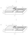
- FIG. 1 is a schematic diagram showing the structure of an antenna module 1 according to an embodiment of the present invention.
- the antenna module 1 has a layer structure in which a substrate 2, a graphene layer 3, and a gallium nitride (GaN) layer 4 are laminated in this order. Then, as shown in FIG. 1, the antenna module 1 realizes the antenna element section 10, the active element section 12, and the connection section 14 by using the layer structure described above.
- GaN gallium nitride
- the substrate 2 serves as a base for forming the graphene layer 3. At least the uppermost surface 21 of the substrate 2 in contact with the graphene layer 3 is made of single crystal silicon carbide (SiC). A portion of the substrate 2 other than the top surface may be an insulator different from SiC. That is, the substrate 2 may be a SiC single crystal substrate or a hybrid substrate in which a SiC single crystal layer is formed on an insulator. The surface of the SiC single crystal layer in the substrate 2 is preferably the (0001) plane.
- the substrate 2 serves as a base for epitaxially growing graphene forming the graphene layer 3 .
- the graphene layer 3 is provided in contact with the top surface of the substrate 2 .
- the graphene layer 3 is composed of single-layer or multiple-layer single crystal graphene.
- Graphene layer 3 functions as a buffer layer between substrate 2 and GaN layer 4 . Further, the graphene layer 3 is patterned into a desired antenna shape to form the antenna element portion 10 and the connection portion 14 .
- the GaN layer 4 is provided on the substrate 2 .
- the GaN layer 4 is provided over the graphene layer 3 as shown in FIG. 1(a).
- the GaN layer 4 may be provided directly on the substrate 2 without the graphene layer 3 interposed therebetween, as shown in FIG. 1(b).
- an amplifier and the like constituting the active element section 12 are formed using elements capable of high-speed operation such as HEMT (High Electron Mobility Transistor).
- a metal film for example, an Au film for forming an electrode or a wiring pattern overlying the graphene layer 3 or the GaN layer 4, a protective film, or the like is provided as necessary.
- the antenna element section 10 In the antenna module 1 having the layer structure of the substrate 2 , the graphene layer 3 , and the GaN layer 4 , the antenna element section 10 , the active element section 12 , and the connection section 14 are provided by partitioning areas on the plane of the substrate 2 .
- the active element section 12 is provided on the GaN layer 4 .
- the active element section 12 may include active elements other than the amplifier described above.
- the active element section 12 may include an electrode 42 to which wiring from the outside (for example, the antenna element section 10 and the connection section 14) is connected.
- the electrode 42 may be provided on the surface of the GaN layer 4 facing the substrate 2 , or may be provided on the surface opposite to the surface facing the substrate 2 .
- the GaN layer 4 is not provided in the antenna element section 10 .
- the antenna element section 10 has a structure in which the graphene layer 3 is patterned into a shape for realizing desired antenna characteristics.
- a metal film such as Au may be provided so as to overlap part or all of the patterned graphene.
- graphene Compared to metals such as copper (Cu) and ITO, graphene has high values for various characteristics such as electrical conductivity, carrier mobility, and thermal conductivity, so it is possible to realize antenna characteristics that surpass Cu. Characteristic deterioration can be suppressed even if the size of the antenna is reduced.
- connection portion 14 is wiring that connects the electrode 42 of the amplifier of the active element portion 12 and the antenna element portion 10 .
- the connecting portion 14 may not be provided with the GaN layer 4 in the same manner as the antenna element portion 10, or may be provided with the GaN layer 4 overlying part or all of it.
- the connection part 14 may be formed by patterning the graphene layer 3, or may be formed of a metal film such as Au.
- the connection part 14 may be partially formed of a metal film and the other part may be formed of graphene, or may have a portion in which the metal film is superimposed on the graphene. Note that transparent wiring can be realized by forming the antenna element portion 10 and the connection portion 14 only from graphene.
- the connecting portion 14 is made as short as possible (for example, preferably less than 100 ⁇ m, more preferably less than 30 ⁇ m, still more preferably less than 10 ⁇ m) so that signals transmitted between the active element portion 12 and the antenna element portion 10 are not degraded. distance).
- the electrode 42 When the electrode 42 is provided on the surface of the GaN layer 4 facing the substrate 2, as shown in FIG. It is preferable to connect indirectly by sandwiching Further, when the electrode 42 is provided on the surface of the GaN layer 4 opposite to the surface facing the substrate 2, the electrode 42 and the connecting portion 14 are connected by wire bonding 14a as shown in FIG. 2(b). You may Alternatively, as shown in FIG. 2(c), a conductor layer 14b made of metal, graphene, or the like may be added to connect the electrodes 42 to the connecting portions 14. FIG.
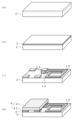
- FIG. 3 is a diagram showing a first example of a procedure for manufacturing an antenna module.
- the substrate 2 is first prepared (FIG. 3(a)). At least the uppermost surface of the substrate 2 is made of single crystal SiC, as described above.
- the crystal structure of SiC on the uppermost surface is preferably 4H--SiC, 6H--SiC, or 3C--SiC.
- a hybrid substrate in which a SiC single crystal layer is formed on an insulator is used as the substrate 2 instead of a SiC single crystal substrate, single crystal silicon, sapphire, polycrystalline silicon, alumina, silicon nitride, aluminum nitride, diamond, A film of silicon oxide, single crystal silicon, polycrystalline silicon, amorphous silicon, alumina, silicon nitride, silicon carbide, aluminum nitride, or diamond is provided thereon as needed, using any of polycrystalline SiC as a base substrate, A bonding surface of the base substrate and the silicon carbide substrate is subjected to a surface treatment and then bonded.
- the SiC single crystal layer is thinned by ion implantation delamination method in which hydrogen ions, helium ions, etc. are implanted into the silicon carbide substrate before thinning by grinding or delamination, and delamination is performed at the ion implantation interface by heat treatment after bonding. It is sufficient to produce a modified hybrid substrate. Further, it is preferable to obtain a hybrid substrate in which a single crystal layer of SiC is formed as an insulator by removing the base substrate after the surface of the hybrid substrate is subjected to CVD with polycrystalline SiC.
- the substrate 2 is preferably heated to 1,100° C. or higher to sublimate silicon atoms (Si) in the vicinity of the uppermost surface of the substrate 2, thereby forming graphene having a desired thickness (for example, about 50 to 1,500 nm).
- a film is formed to form the graphene layer 3 (FIG. 3(b)).
- heating may be performed under an argon (Ar) atmosphere at a pressure of 10 5 Pa (1 bar) and a temperature of 1500 to 1600° C. for 5 to 30 minutes.
- Ar argon
- a nanocarbon film of any one of fullerene, graphene, and carbon nanotube is formed, and graphene is obtained by appropriately adjusting the preparation conditions.
- the graphene layer 3 thus formed undergoes so-called epitaxial growth so that the crystals are oriented in a predetermined direction with respect to the crystal plane of the SiC single crystal on the uppermost surface of the substrate 2 as a base.
- GaN gallium nitride
- MOCVD metal organic chemical vapor deposition
- TMGa trimethylgallium
- TMAl trimethylaluminum
- NH 3 ammonia
- the substrate 2 provided with the graphene layer 3 may be thermally cleaned in an H 2 atmosphere at 1100° C. for about 5 minutes. It is preferable to grow an AlN buffer layer of several tens to several hundred nm on the surface of the substrate after cleaning, and then grow an undoped GaN layer 4 having a thickness of approximately 2 ⁇ m at 1050°C.
- the AlN buffer layer is preferably grown such that a high-temperature AlN buffer layer grown at about 1080° C. is stacked on a low-temperature AlN buffer layer grown at about 780° C.
- the graphene layer 3 was used as the nucleation layer (template layer) of the GaN epicrystal, but before the growth of the GaN epicrystal, the portion where GaN is grown (that is, the portion where the active element portion is provided)
- the graphene layer 3 may be removed and GaN may be grown directly on the SiC single crystal on the uppermost surface 21 of the substrate 2 .
- Active elements such as HEMTs, passive elements such as resistors, capacitors, and inductors, wiring, electrodes 42, and the like are formed on the formed GaN layer 4 to form an active element section 12 including an amplifier and the like (FIG. 3 ( d)).
- the GaN layer 4 is removed from the portions other than the active element portion 12 by etching to expose the graphene layer 3 (FIG. 3(e)). Further, the graphene layer 3 is patterned to form the antenna element portion 10 and the connection portion 14 (FIG. 3(f)). This patterning is performed, for example, by evaporating an Au film on the graphene layer 3, patterning the Au film by photolithography technology and etching technology, and exposing graphene not covered with the Au film by UV-ozone treatment or the like. It is preferable to remove the Au film and then remove unnecessary portions of the Au film.
- the electrode 42 of the active element section 12 and the connection section 14 are electrically connected (FIG. 3(g)).
- the electrode 42 and the connecting portion 14 may be connected by wire bonding (FIG. 2(b)), or may be connected by adding graphene or a metal thin film (FIG. 2(c)).
- a monolithic antenna module in which the antenna element section 10 and the active element section 12 are provided on the substrate 2 and connected by the connection section 14 can be manufactured.
- the formation of the active element portion 12 and the formation of the antenna element portion 10 and the connection portion 14 may be performed in a different order, or part or all of the steps may be performed simultaneously.
- the antenna element section 10 and the active element section 12 are provided close to each other, and are connected by a very short connection section 14. Therefore, signals from several tens of GHz to 100 GHz or more can be generated. Also in the frequency band, deterioration of signals propagating between the antenna element section 10 and the active element section 12 can be suppressed.
- the graphene layer 3 is a single crystal film formed by epitaxial growth on the SiC single crystal on the uppermost surface of the substrate 2 .
- graphene has superior properties (conductivity, carrier mobility, thermal conductivity, film strength, etc.) as compared to the technique of transferring a separately prepared polycrystalline graphene film to a substrate.
- Antenna elements obtained by patterning such single-crystal graphene are expected to have superior characteristics not only to antenna elements made of metal thin films such as copper, but also to antenna elements made of polycrystalline graphene. , the characteristics are less likely to deteriorate even if the size of the antenna is further reduced.
- both the graphene layer 3 and the GaN layer 4 are formed such that the crystals are oriented in predetermined directions with respect to the crystal plane of the SiC single crystal on the uppermost surface of the substrate 2 .
- the graphene layer 3 and the GaN layer 4 are oriented so that their respective crystals form a relatively predetermined angle.
- FIG. 4 is a diagram showing a second example of the procedure for manufacturing an antenna module.
- the GaN layer 4 is not epitaxially grown, but a separate GaN device 41 is prepared, and the GaN layer is provided by bonding the GaN device 41 to the substrate 2 on which the graphene layer 3 is provided. Different from the example.
- the substrate 2 is prepared by the same method as described with reference to FIGS. 3A and 3B (FIG. 4A), A graphene layer 3 is formed on the uppermost surface of the substrate 2 (FIG. 4(b)).
- the graphene layer 3 is patterned to form the antenna element portion 10 and the connection portion 14 (FIG. 4(c)). Further, when the GaN device 41 is attached in the subsequent stage, the electrode pads 15 to be connected to the electrodes 42 of the active element section 12 are also patterned so as to extend from the connection section 14 . Alternatively, a pattern of the graphene layer 3 (or an Au film provided thereon) necessary for bonding with the GaN device 41 may be formed. That is, the graphene layer 3 may function as an adhesive layer for attaching the active element section 12 to the substrate 2 .
- the antenna element section 10 can be monolithically formed on the substrate 2 .
- the pattern used for bonding to the GaN device 41 may be formed by removing the graphene layer 3 and forming only a metal thin film such as Au.
- the pattern used for bonding with the GaN device 41 may be made of graphene, a metal thin film, or a laminate of these.
- the pattern used for bonding with the GaN device 41 may also have the function of ensuring electrical connection between the elements in the GaN device 41 and the outside, similar to the electrode pads 15 connected to the electrodes 42 .
- a separately prepared GaN device 41 is attached to an appropriate position on the substrate 2 (Fig. 4(d)).
- the GaN device 41 is obtained by forming an element such as an amplifier constituting the active element section 12 on a GaN substrate and cutting it into a predetermined size.
- the surface of the GaN device 41 (the surface bonded to the substrate 2) is provided with an electrode 42 for exchanging signals with elements in the active element section 12.
- FIG. When bonding the GaN device 41 and the substrate 2 together, the electrodes 42 of the GaN device 41 and the electrode pads 15 on the substrate 2 are electrically connected.
- the bonding of the GaN device 41 and the substrate 2 is preferably performed after the surfaces of both are subjected to activation treatment or surface treatment.
- the GaN device 41 can be attached to the substrate 2 by flip-chip bonding.
- the GaN device 41 attached to the substrate 2 becomes the GaN layer 4 in the antenna module 1 .
- an integrated antenna module in which the antenna element section 10 and the active element section 12 are provided on the substrate 2 and are connected by the connection section 14 can be manufactured.
- the antenna element section 10 and the active element section 12 are provided close to each other, and are connected by a very short connection section 14. Therefore, signals from several tens of GHz to 100 GHz or more can be generated. Also in the frequency band, deterioration of signals propagating between the antenna element section 10 and the active element section 12 can be suppressed.
- the graphene layer 3 is a single crystal film formed by epitaxial growth on the SiC single crystal on the uppermost surface of the substrate 2 .
- graphene has superior properties (conductivity, carrier mobility, thermal conductivity, film strength, etc.) as compared to the technique of transferring a separately prepared polycrystalline graphene film to a substrate.
- Antenna elements obtained by patterning such single-crystal graphene are expected to have superior characteristics not only to antenna elements made of metal thin films such as copper, but also to antenna elements made of polycrystalline graphene. , the characteristics are less likely to deteriorate even if the size of the antenna is further reduced.
- the GaN device 41 having the active element portion 12 formed thereon can be prepared separately and then bonded to the substrate 2, so that the active element portion 12 can be designed freely. expensive. Also, by preparing a plurality of types of GaN devices 41 that are bonded to each other with different functions and performances, it is possible to manufacture various variations of the antenna module 1 while using the antenna element section 10 in common.
- the present invention is not limited to the above embodiments and examples.
- the antenna element portion 10 and the active element portion 12 are provided on the same surface of the substrate 2, but as shown in FIG. may be provided on the surface opposite to the surface on which is provided.
- the connecting portion 14 that connects the antenna element portion 10 and the active element portion 12 preferably includes a through-substrate via 14c that penetrates the substrate 2 and electrically connects both surfaces.
- the graphene layers 3 are provided on both sides of the substrate 2, and the wiring of the connection portion 14 drawn out to the active element portion 12, the electrode pads that are joined to the active element portion 12, and the antenna element portion 10 are formed of graphene.
- the electrode 42 is provided on the substrate bonding surface of the active element section 12, and the electrode pad 15 on the substrate 2 and the electrode 42 are directly connected.
- the electrode 42 may be provided on the surface of the GaN layer 4 opposite to the surface facing the substrate 2 .
- the electrode pads 15 are not provided on the substrate, and the electrodes 42 and the connection portions 14 are preferably connected by wire bonding or addition of a conductor layer as shown in FIG. 2(b).
- Antenna Module 2 Substrate 3 Graphene Layer 4 GaN Layer 10 Antenna Element Section 12 Active Element Section 14 Connection Section 15 Electrode Pad 41 GaN Device 42 Electrode
Landscapes
- Chemical & Material Sciences (AREA)
- Engineering & Computer Science (AREA)
- Organic Chemistry (AREA)
- Materials Engineering (AREA)
- Nanotechnology (AREA)
- Inorganic Chemistry (AREA)
- Microelectronics & Electronic Packaging (AREA)
- Manufacturing & Machinery (AREA)
- Composite Materials (AREA)
- Junction Field-Effect Transistors (AREA)
- Details Of Aerials (AREA)
- Carbon And Carbon Compounds (AREA)
- Variable-Direction Aerials And Aerial Arrays (AREA)
- Semiconductor Integrated Circuits (AREA)
Abstract
数10GHzから100GHz以上の信号周波数帯域での使用に適したアンテナモジュールを提供する。 アンテナモジュールは、少なくとも最上面が炭化珪素の単結晶である基板と、前記基板の最上面に接して設けられた単結晶のグラフェン層と、前記基板上に設けられた窒化ガリウム層とを備える。そして、このアンテナモジュールは、前記グラフェン層における前記窒化ガリウム層に覆われていない領域をパターニングにして形成されたアンテナエレメント部と、前記窒化ガリウム層に形成されたアクティブ素子部と、前記アンテナエレメント部と前記アクティブ素子部とを接続する接続部とが一体的に形成されたことを特徴とする。
Description
本発明は、グラフェンをアンテナエレメントおよび/または配線として用い、増幅器等のアクティブ素子と一体に形成されたアンテナモジュールに関する。
次世代の移動通信システム(いわゆる6G、Beyond5G)を実現するにあたり、100GHz以上といった高周波での送受信に適した、高性能のアンテナが求められている。このようなアンテナの候補として、従来アンテナエレメントにおける導体として用いられた銅、ITO(Indiumtinoxide)等と比較して優れた特性(高導電率、高キャリア移動度、高熱伝導率)を有するグラフェンをアンテナエレメントに用いたアンテナが提案されている(例えば特許文献1を参照)。
特許文献1に記載されているマイクロ波帯アンテナは、銅箔上にCVD法により形成したグラフェン膜を基板に転写し、転写したグラフェン膜上に適宜Au膜を設けつつ、フォトリソグラフィ技術、エッチング技術、UV-オゾン処理等によりパターニングすることでアンテナエレメントを形成する。これにより、基板上に所望の形状のアンテナエレメントを作製することができる。
ところで、移動通信システムに用いるアンテナは、アンテナエレメントで送受信する信号を増幅する増幅器とともに用いられる。数10GHzから100GHz以上の信号周波数帯域では、増幅器とアンテナエレメントとの間の伝送距離は、(例えば100μm未満となるように)極短くする必要がある。
しかし、特許文献1は、アンテナエレメント単体としての実現性を示すのみであり、増幅器等と組み合わせたデバイスへの応用については具体的な教示がない。
本発明は上記に鑑みなされたものであり、数10GHzから100GHz以上の信号周波数帯域での使用に適したアンテナモジュールを提供することを目的とする。
本発明の実施形態に係るアンテナモジュールは、少なくとも最上面が炭化珪素の単結晶である基板と、基板の最上面に接して設けられた単結晶のグラフェン層と、基板上に設けられた窒化ガリウム層とを備える。そして、このアンテナモジュールは、グラフェン層における窒化ガリウム層に覆われていない領域をパターニングにして形成されたアンテナエレメント部と、窒化ガリウム層に形成されたアクティブ素子部と、アンテナエレメント部とアクティブ素子部とを接続する接続部とが一体的に形成されたことを特徴とする。
本発明では、窒化ガリウム層は、グラフェン層の一部を覆うように設けられるとよい。
本発明では、基板は、絶縁体のベース基板上に炭化珪素の単結晶層を作製したハイブリッド基板とするとよい。
本発明では、窒化ガリウム層は、グラフェン層をバッファ層としてエピタキシャル成長された層とするとよい。
本発明では、アクティブ素子部は窒化ガリウム層内に形成されたHEMT(High Electron Mobility Transistor)を用いた増幅器を含むとよい。
本発明では、接続部は100μm未満の長さでアンテナエレメント部とアクティブ素子部とを接続するとよい。
また、本発明の一実施形態に係るアンテナモジュールの製造方法は、少なくとも最上面が炭化珪素の単結晶である基板を用意するステップと、基板の最上面にグラフェン層を形成するステップと、グラフェン層をバッファ層として窒化ガリウム層をエピタキシャル成長するステップと、窒化ガリウム層に増幅器を含むアクティブ素子部を形成するステップと、窒化ガリウム層におけるアクティブ素子部が設けられていない領域を除去してグラフェン層を露出させるステップと、露出したグラフェン層をパターニングしてアンテナエレメントおよびアクティブ素子部とアンテナエレメントとを接続する接続部を形成するステップと、を含む。
また、本発明の他の実施形態に係るアンテナモジュールの製造方法は、少なくとも最上面が炭化珪素の単結晶である基板を用意するステップと、基板の最上面にグラフェン層を形成するステップと、グラフェン層の一部を除去するとともに、グラフェン層をパターニングしてアンテナエレメントおよびアクティブ素子部とアンテナエレメントとを接続する接続部を形成するステップと、グラフェン層が除去された領域に、窒化ガリウム層をエピタキシャル成長するステップと、窒化ガリウム層に増幅器を含むアクティブ素子部を形成するステップと、を含む。
また、本発明のさらに他の実施形態に係るアンテナモジュールの製造方法は、少なくとも最上面が炭化珪素の単結晶である基板を用意するステップと、基板の最上面にグラフェン層を形成するステップと、グラフェン層をパターニングしてアンテナエレメントを形成するステップと、増幅器を含むアクティブ素子部が形成された窒化ガリウムデバイスを、基板上のグラフェン層に貼り合わせて窒化ガリウム層を設けるステップと、を含む。
本発明では、アンテナエレメントを形成するステップにおいて、アンテナエレメントとともに、電極パッドおよびアンテナエレメントと電極パッドとを接続する接続部を形成し、窒化ガリウム層を設けるステップにおいて、窒化ガリウムデバイスに設けられた電極と、電極パッドとが電気的に接続されるように、窒化ガリウムデバイスを基板上のグラフェン層に貼り合わせるとよい。
上述のアンテナモジュールの各製造方法におけるグラフェン層を形成するステップにおいて、基板の最上面の炭化珪素の単結晶における珪素原子を昇華させることによりグラフェン層をエピタキシャル成長させるとよい。
上述のアンテナモジュールの各製造方法において、基板は、絶縁体のベース基板上に炭化珪素の単結晶層を作製したハイブリッド基板とするとよい。
本発明のアンテナモジュールおよびその製造方法によれば、グラフェンを用いたアンテナエレメントと、増幅器等のアクティブ素子とが一体に形成され、数10GHzから100GHz以上の信号周波数帯域での使用に適したアンテナモジュールを実現することができる。
以下、本発明の実施形態について説明する。背景技術の説明に用いた図も含め、各図面における共通の構成要素については同じ符号を付す。
図1は、本発明の実施形態に係るアンテナモジュール1の構造を示す模式図である。図1に示すように、アンテナモジュール1は、基板2、グラフェン層3、および窒化ガリウム(GaN)層4がこの順に積層された層構成を有する。そして、アンテナモジュール1は、図1に示すように、前記の層構成を利用して、アンテナエレメント部10、アクティブ素子部12、および接続部14を実現する。
基板2は、グラフェン層3を形成するための下地となる。基板2は、少なくともグラフェン層3と接する最上面21が単結晶の炭化珪素(SiC)となっている。基板2の最上面以外の部分はSiCとは異なる絶縁体であってもよい。つまり、基板2は、SiCの単結晶基板であってもよいし、絶縁体にSiCの単結晶層を作製したハイブリッド基板であってもよい。基板2におけるSiCの単結晶層の表面は(0001)面とするとよい。基板2は、グラフェン層3を成すグラフェンをエピタキシャル成長させるための下地となる。
グラフェン層3は、基板2の最上面に接して設けられる。グラフェン層3は単層または複数層の単結晶のグラフェンにより構成される。グラフェン層3は、基板2とGaN層4の間でバッファ層として機能する。また、グラフェン層3は、所望のアンテナ形状にパターニングされることでアンテナエレメント部10および接続部14を構成する。
GaN層4は、基板2の上に設けられる。一例として、GaN層4は、図1(a)に示したようにグラフェン層3に重ねて設けられる。他の例としては、図1(b)に示したように、GaN層4は、グラフェン層3を介さずに基板2の上に直接設けられてもよい。GaN層4には、アクティブ素子部12を構成する増幅器等が、HEMT(High Electron Mobility Transistor)等の高速動作が可能な素子を用いて形成される。
なお、図1には示されていないが、必要に応じてグラフェン層3やGaN層4に重ねて電極や配線パターンを形成するための金属膜(例えばAu膜)や、保護膜等が設けられてもよい。
基板2、グラフェン層3、およびGaN層4の層構成によるアンテナモジュール1において、アンテナエレメント部10、アクティブ素子部12、および接続部14は、基板2の平面において領域を区画して設けられる。図1に示すように、アクティブ素子部12はGaN層4に設けられる。アクティブ素子部12は、上述の増幅器に加えそれ以外のアクティブ素子を備えてもよい。アクティブ素子部12は外部(例えばアンテナエレメント部10や接続部14)からの配線が接続される電極42を備えてもよい。電極42は、GaN層4の基板2と対向する面に設けられてもよいし、基板2と対向する面とは反対の面に設けられてもよい。
アンテナエレメント部10には、GaN層4が設けられない。アンテナエレメント部10は、グラフェン層3が所望のアンテナ特性を実現するための形状にパターニングされた構造を有する。パターニングされたグラフェンの一部または全部に重畳してAu等の金属膜が設けられもよい。グラフェンは銅(Cu)をはじめとする金属やITOと比べて、導電率、キャリア移動度、熱伝導率等の諸特性が高い値を有するため、Cuを凌ぐアンテナ特性を実現することができ、アンテナのサイズを縮小しても特性劣化を抑制することができる。
接続部14は、アクティブ素子部12の増幅器の電極42とアンテナエレメント部10とを接続する配線である。接続部14には、アンテナエレメント部10と同様にGaN層4が設けられないようにしてもよいし、その一部または全部にGaN層4が重ねて設けられていてもよい。接続部14は、グラフェン層3をパターニングすることにより形成されてもよいし、Au等の金属膜により形成されてもよい。また、接続部14は、一部が金属膜により形成され、他の部分がグラフェンにより形成されてもよく、グラフェンに金属膜が重畳して設けられている部分があってもよい。なお、アンテナエレメント部10や接続部14をグラフェンのみで形成すると、透明配線を実現することができる。接続部14は、アクティブ素子部12とアンテナエレメント部10との間で伝送される信号が劣化しないよう、極力短く(例えば、好ましくは100μm未満、より好ましくは30μm未満、さらに好ましくは10μm未満の伝送距離となるように)形成されることが好ましい。
電極42が、GaN層4の基板2と対向する面に設けられる場合には、図2(a)に示すように、電極42と接続部14の一端に設けられる電極パッド15とが直接または導体を挟んで間接的に接続されるようにするとよい。また、電極42がGaN層4の基板2と対向する面とは反対の面に設けられる場合には、図2(b)に示すように、ワイヤボンディング14aにより電極42と接続部14とを接続してもよい。あるいは、図2(c)に示すように、金属、グラフェン等の導体層14bを付加して電極42接続部14とを接続してもよい。
続いて、アンテナモジュール1の製造方法について説明する。
図3は、アンテナモジュールの作製する手順の第1の例を示す図である。
図3は、アンテナモジュールの作製する手順の第1の例を示す図である。
図3に示すように、はじめに基板2を用意する(図3(a))。基板2は、上述の通り、少なくとも最上面が単結晶のSiCとなっている。この最上面のSiCの結晶構造は、4H-SiC、6H-SiC、3C-SiCのいずれかであることが好ましい。
基板2としてSiCの単結晶基板ではなく、絶縁体にSiCの単結晶層を作製したハイブリッド基板を用いる場合には、単結晶シリコン、サファイヤ、多結晶シリコン、アルミナ、窒化珪素、窒化アルミニウム、ダイヤモンド、多結晶SiCの何れかをベース基板として、その上に必要に応じて酸化シリコン、単結晶シリコン、多結晶シリコン、アモルファスシリコン、アルミナ、窒化珪素、炭化珪素、窒化アルミニウム、またはダイヤモンドの膜を設け、ベース基板及び炭化珪素基板の貼り合わせ面に表面化処理を施して貼り合わせをする。その後、研削研磨による薄化や剥離前の炭化珪素基板に水素イオンやヘリウムイオン等を注入し、貼り合せ後に熱処理によりイオン注入界面で剥離を行うイオン注入剥離法等によりSiCの単結晶層を薄化したハイブリッド基板を作製すればよい。また、上記ハイブリッド基板を作製後に表面を多結晶SiCでCVDしたのちに上記ベース基板を除去して絶縁体にSiCの単結晶層を作製したハイブリッド基板を得るとよい。
続いて、基板2を好ましくは1,100℃以上に加熱することにより基板2の最上面近傍の珪素原子(Si)を昇華させて、所望の厚さ(例えば50~1,500nm程度)のグラフェン膜を形成し、グラフェン層3とする(図3(b))。グラフェンの典型的な成長条件の一例としては、アルゴン(Ar)雰囲気下で気圧105Pa(1bar)、1500~1600℃の温度で、5~30分間加熱するとよい。Siを昇華した際には、フラーレン、グラフェン、カーボンナノチューブの何れかのナノカーボン膜が形成されるが、作成条件を適宜調整してグラフェンが得られるようにする。このようにして形成されるグラフェン層3は、下地となる基板2の最上面のSiC単結晶の結晶面に対して所定の向きに結晶が配向するように、いわゆるエピタキシャル成長する。
続いて、グラフェン層3をバッファ層(すなわち、GaNエピ結晶の核形成層(テンプレート層))として、窒化ガリウム(GaN)をエピタキシャル成長させ、GaN層4を形成する(図3(c))。GaNは、例えば有機金属気相成長法(MOCVD法)によりエピタキシャル成長させるとよい。具体的には、Ga、Al、Nの前駆体として、それぞれトリメチルガリウム(TMGa)、トリメチルアルミニウム(TMAl)、アンモニア(NH3)を用い、キャリアガスにはH2とN2を用いるとよい。成膜に先立ち、グラフェン層3を設けた基板2をH2雰囲気中、1100℃で5分間程度の熱洗浄を行うとよい。洗浄後の基板表面に、AlNバッファ層を数10~数100nm程度成長させ、その後、1050℃で厚さ2μm程度のアンドープのGaN層4を成長させるとよい。AlNバッファ層は、780℃程度で成長させた低温のAlNバッファ層の上に1080℃程度で成長させた高温のAlNバッファ層が積層されるように成長させるとよい。なお、上記の例ではグラフェン層3をGaNエピ結晶の核形成層(テンプレート層)としたが、GaNエピ結晶の成長前に、GaNを成長させる部位(つまり、アクティブ素子部が設けられる部分)についてグラフェン層3を除去して、基板2の最上面21のSiC単結晶にGaNを直接成長するようにしてもよい。
そして、形成したGaN層4に、HEMT等のアクティブ素子、抵抗、キャパシタ、インダクタ等のパッシブ素子、配線、電極42等を形成して、増幅器等を含むアクティブ素子部12を形成する(図3(d))。
続いて、エッチングによりアクティブ素子部12以外の部分からGaN層4を除去し、グラフェン層3を露出させる(図3(e))。さらに、グラフェン層3にアンテナエレメント部10と接続部14をパターニングする(図3(f))。このパターニングは、例えば、グラフェン層3にAu膜を蒸着した上で、Au膜に対しフォトリソグラフィ技術およびエッチング技術によりパターニングを行い、Au膜で覆われていない露出したグラフェンをUV-オゾン処理等により除去し、さらにAu膜の不要部分を除去する、という手順で行うとよい。
最後に、アクティブ素子部12の電極42と、接続部14とを電気的に接続する(図3(g))。なお、電極42と接続部14とは、ワイヤボンディングにより接続してもよい(図2(b))し、グラフェンや金属薄膜を付加することで接続してもよい(図2(c))。
以上のような手順により、基板2上にアンテナエレメント部10とアクティブ素子部12が設けられ、両者が接続部14によって接続されたモノリシックのアンテナモジュールを作製することができる。なお、アクティブ素子部12の形成とアンテナエレメント部10および接続部14の形成は、順番を入れ替えて行ってもよいし、工程の一部または全部を同時に行ってもよい。
上記のようにして作成されたアンテナモジュール1は、アンテナエレメント部10とアクティブ素子部12が近接して設けられ、両者がごく短い接続部14にて接続されるため、数10GHzから100GHz以上の信号周波数帯域においても、アンテナエレメント部10とアクティブ素子部12との間を伝搬する信号の劣化を抑制することができる。
また、上記の手順で作製されたアンテナモジュール1では、グラフェン層3は、基板2の最上面のSiC単結晶上にエピタキシャル成長により形成された単結晶の膜となる。このため、別途作製した多結晶のグラフェンの膜を基板に転写する手法と比較して、グラフェンの特性(導電率、キャリア移動度、熱伝導性、膜の強度等)が優れたものとなる。このような単結晶のグラフェンをパターニングにして得られるアンテナエレメントは、銅等の金属薄膜で作製されたアンテナエレメントはもとより、多結晶グラフェン作製されたアンテナエレメントと比較しても優れた特性が期待でき、アンテナのサイズをより小型化しても特性が劣化しにくい。
また、上記の手順で作製されたアンテナモジュール1では、グラフェン層3だけでなくGaN層4もエピタキシャル成長により形成される。したがって、グラフェン層3およびGaN層4は、いずれも基板2の最上面のSiC単結晶の結晶面に対してそれぞれ所定の向きに結晶が配向するように形成される。つまり、グラフェン層3とGaN層4とは、それぞれの結晶が相対的に予め決まった角度を成すように配向することになる。これにより、GaN-HEMTとグラフェン・アンテナ間の電気抵抗や寄生抵抗を抑制することができ、アンテナの放射効率等の特性を向上することができる。
図4は、アンテナモジュールの作製する手順の第2の例を示す図である。この手順では、GaN層4をエピタキシャル成長せずに、別途GaNデバイス41を用意し、グラフェン層3が設けられた基板2にGaNデバイス41を貼り合わせることによりGaN層を設ける点で前記の第1の例と異なる。
アンテナモジュールの作製する手順の第2の例では、まず、図3(a)および(b)を参照して説明したのと同様の手法により、基板2を用意し(図4(a))、基板2の最上面にグラフェン層3を形成する(図4(b))。
続いて、グラフェン層3にアンテナエレメント部10と接続部14をパターニングする(図4(c))。また、後段においてGaNデバイス41を貼り合わせる際に、アクティブ素子部12の電極42と接続される電極パッド15も接続部14から延伸する形でパターニングする。その他、GaNデバイス41との接合に必要なグラフェン層3(またはその上に設けられるAu膜)のパターンを形成してもよい。つまり、グラフェン層3は、アクティブ素子部12を基板2に貼りつけるための接着層として機能してもよい。これらのパターニングは、例えば、グラフェン層3にAu膜を蒸着した上で、Au膜に対しフォトリソグラフィ技術およびエッチング技術によりパターニングを行い、Au膜で覆われていない露出したグラフェンをUV-オゾン処理等により除去し、さらにAu膜の不要部分を除去する、という手順で行うとよい。このようにして、基板2上にアンテナエレメント部10をモノリシックに形成することができる。なお、GaNデバイス41との接合に用いられるパターンは、グラフェン層3を除去してAu等の金属薄膜のみにより形成してもよい。GaNデバイス41との接合に用いるパターンは、グラフェンによるもの、金属薄膜によるもの、あるいはこれらを積層したものであってよい。GaNデバイス41との接合に用いられるパターンは、電極42と接続される電極パッド15と同様に、GaNデバイス41内の素子と外部との電気的接続を確保する機能を兼ねてもよい。
続いて、別途用意したGaNデバイス41を、基板2の適切な位置に貼り合わせる(図4(d))。GaNデバイス41は、GaNの基板上に、アクティブ素子部12を構成する増幅器等の素子を形成して所定の寸法に切り出したものである。GaNデバイス41の表面(基板2に張り合わされる面)は、アクティブ素子部12内の素子と信号の授受を行うための電極42が設けられる。GaNデバイス41と基板2とを貼り合わせる際、GaNデバイス41の電極42と基板2上の電極パッド15とが電気的に接続される。GaNデバイス41と基板2との貼り合わせは、両者の表面に対し、活性化処理や表面処理を行った上で実施するとよい。また、GaNデバイス41をフリップチップボンディングによって基板2に貼り合わせることもできる。基板2に貼り合わされたGaNデバイス41は、アンテナモジュール1におけるGaN層4となる。
以上のような手順により、基板2上にアンテナエレメント部10とアクティブ素子部12が設けられ、両者が接続部14によって接続された一体のアンテナモジュールを作製することができる。
上記のようにして作成されたアンテナモジュール1は、アンテナエレメント部10とアクティブ素子部12が近接して設けられ、両者がごく短い接続部14にて接続されるため、数10GHzから100GHz以上の信号周波数帯域においても、アンテナエレメント部10とアクティブ素子部12との間を伝搬する信号の劣化を抑制することができる。
また、上記の手順で作製されたアンテナモジュール1では、グラフェン層3は、基板2の最上面のSiC単結晶上にエピタキシャル成長により形成された単結晶の膜となる。このため、別途作製した多結晶のグラフェンの膜を基板に転写する手法と比較して、グラフェンの特性(導電率、キャリア移動度、熱伝導性、膜の強度等)が優れたものとなる。このような単結晶のグラフェンをパターニングにして得られるアンテナエレメントは、銅等の金属薄膜で作製されたアンテナエレメントはもとより、多結晶グラフェン作製されたアンテナエレメントと比較しても優れた特性が期待でき、アンテナのサイズをより小型化しても特性が劣化しにくい。
また、上記の手順で作製されたアンテナモジュール1では、アクティブ素子部12が形成されたGaNデバイス41を別途用意してから基板2に貼り合わせることもできるため、クティブ素子部12の設計自由度が高い。また、貼り合わせるGaNデバイス41を、機能や性能が異なる複数種類準備すれば、アンテナエレメント部10を共通としつつ、様々なバリエーションのアンテナモジュール1を作ることができる。
〔実施形態の変形〕
なお、本発明は上記の実施形態や実施例に限定されるものではない。
例えば、上記の実施形態では、アンテナエレメント部10とアクティブ素子部12が基板2の同一面上に設けられたが、図5に示すように、アンテナエレメント部10が、基板2におけるアクティブ素子部12が設けられる面とは反対の面に設けられてもよい。この場合、アンテナエレメント部10とアクティブ素子部12を接続する接続部14が、基板2を貫通して両面を電気的に接続する基板貫通ビア14cを含むとよい。また、この場合、基板2の両面にグラフェン層3を設け、アクティブ素子部12に引き出される接続部14の配線、アクティブ素子部12と接合する電極パッド、およびアンテナエレメント部10をグラフェンにて形成してもよい。
なお、本発明は上記の実施形態や実施例に限定されるものではない。
例えば、上記の実施形態では、アンテナエレメント部10とアクティブ素子部12が基板2の同一面上に設けられたが、図5に示すように、アンテナエレメント部10が、基板2におけるアクティブ素子部12が設けられる面とは反対の面に設けられてもよい。この場合、アンテナエレメント部10とアクティブ素子部12を接続する接続部14が、基板2を貫通して両面を電気的に接続する基板貫通ビア14cを含むとよい。また、この場合、基板2の両面にグラフェン層3を設け、アクティブ素子部12に引き出される接続部14の配線、アクティブ素子部12と接合する電極パッド、およびアンテナエレメント部10をグラフェンにて形成してもよい。
また、上記の実施形態において、アンテナモジュールの作製する手順の第2の例では、アクティブ素子部12の基板接合面に電極42設けられ、基板2上の電極パッド15と電極42とが直接接続されたが、電極42はGaN層4の基板2と対向する面とは反対の面に設けられてもよい。この場合には、基板上には電極パッド15を設けず、図2(b)に示すように、ワイヤボンディングや導体層の付加により電極42と接続部14とを接続するとよい。
また、本発明の特許請求の範囲に記載された技術的思想と実質的に同一の構成を有し、同様な作用効果を奏するものは、いかなる変更がされたものであっても本発明の技術的範囲に包含される。
1 アンテナモジュール
2 基板
3 グラフェン層
4 GaN層
10 アンテナエレメント部
12 アクティブ素子部
14 接続部
15 電極パッド
41 GaNデバイス
42 電極
2 基板
3 グラフェン層
4 GaN層
10 アンテナエレメント部
12 アクティブ素子部
14 接続部
15 電極パッド
41 GaNデバイス
42 電極
Claims (12)
- 少なくとも最上面が炭化珪素の単結晶である基板と、
前記基板の最上面に接して設けられた単結晶のグラフェン層と、
前記基板上に設けられた窒化ガリウム層と
を備え、
前記グラフェン層における前記窒化ガリウム層に覆われていない領域をパターニングにして形成されたアンテナエレメント部と、
前記窒化ガリウム層に形成されたアクティブ素子部と、
前記アンテナエレメント部と前記アクティブ素子部とを接続する接続部と
が一体的に形成されたことを特徴とするアンテナモジュール。 - 前記窒化ガリウム層は、前記グラフェン層の一部を覆うように設けられることを特徴とする請求項1に記載のアンテナモジュール。
- 前記基板は、絶縁体のベース基板上に炭化珪素の単結晶層を作製したハイブリッド基板であることを特徴とする、請求項1または2に記載のアンテナモジュール。
- 前記窒化ガリウム層は、前記グラフェン層をバッファ層としてエピタキシャル成長された層であることを特徴とする請求項1から3の何れか1項に記載のアンテナモジュール。
- 前記アクティブ素子部は窒化ガリウム層内に形成されたHEMT(High Electron Mobility Transistor)を用いた増幅器を含むことを特徴とする請求項1から4の何れか1項に記載のアンテナモジュール。
- 前記接続部は100μm未満の長さで前記アンテナエレメント部と前記アクティブ素子部とを接続することを特徴とする請求項1から5の何れか1項に記載のアンテナモジュール。
- 少なくとも最上面が炭化珪素の単結晶である基板を用意するステップと、
前記基板の最上面にグラフェン層を形成するステップと、
前記グラフェン層をバッファ層として窒化ガリウム層をエピタキシャル成長するステップと、
前記窒化ガリウム層に増幅器を含むアクティブ素子部を形成するステップと、
前記窒化ガリウム層における前記アクティブ素子部が設けられていない領域を除去して前記グラフェン層を露出させるステップと、
露出した前記グラフェン層をパターニングしてアンテナエレメントおよび前記アクティブ素子部と前記アンテナエレメントとを接続する接続部を形成するステップと、
を含む、アンテナモジュールの製造方法。 - 少なくとも最上面が炭化珪素の単結晶である基板を用意するステップと、
前記基板の最上面にグラフェン層を形成するステップと、
前記グラフェン層の一部を除去するとともに、前記グラフェン層をパターニングしてアンテナエレメントおよび前記アクティブ素子部と前記アンテナエレメントとを接続する接続部を形成するステップと、
前記グラフェン層が除去された領域に、窒化ガリウム層をエピタキシャル成長するステップと、
前記窒化ガリウム層に増幅器を含むアクティブ素子部を形成するステップと、
を含む、アンテナモジュールの製造方法。 - 少なくとも最上面が炭化珪素の単結晶である基板を用意するステップと、
前記基板の最上面にグラフェン層を形成するステップと、
前記グラフェン層をパターニングしてアンテナエレメントを形成するステップと、
増幅器を含むアクティブ素子部が形成された前記窒化ガリウムデバイスを、前記基板上の前記グラフェン層に貼り合わせて窒化ガリウム層を設けるステップと、
を含む、アンテナモジュールの製造方法。 - 前記アンテナエレメントを形成するステップにおいて、前記アンテナエレメントとともに、電極パッドおよび前記アンテナエレメントと前記電極パッドとを接続する接続部を形成し、
前記窒化ガリウム層を設けるステップにおいて、前記窒化ガリウムデバイスに設けられた電極と、前記電極パッドとが電気的に接続されるように、前記窒化ガリウムデバイスを前記基板上の前記グラフェン層に貼り合わせることを特徴とする請求項9に記載のアンテナモジュールの製造方法。 - 前記グラフェン層を形成するステップにおいて、前記基板の最上面の炭化珪素の単結晶における珪素原子を昇華させることによりグラフェン層をエピタキシャル成長させることを特徴とする請求項8から10の何れか1項に記載のアンテナモジュールの製造方法。
- 前記基板は、絶縁体のベース基板上に炭化珪素の単結晶層を作製したハイブリッド基板であることを特徴とする、請求項8から11の何れか1項に記載のアンテナモジュールの製造方法。
Priority Applications (4)
| Application Number | Priority Date | Filing Date | Title |
|---|---|---|---|
| CN202280083505.1A CN118541876A (zh) | 2021-12-21 | 2022-10-21 | 天线模块和其制造方法 |
| EP22910555.6A EP4456331A4 (en) | 2021-12-21 | 2022-10-21 | ANTENNA MODULE AND ITS MANUFACTURING PROCESS |
| KR1020247018461A KR20240127343A (ko) | 2021-12-21 | 2022-10-21 | 안테나 모듈 및 그 제조 방법 |
| US18/712,840 US20240339747A1 (en) | 2021-12-21 | 2022-10-21 | Antenna module and manufacturing method thereof |
Applications Claiming Priority (2)
| Application Number | Priority Date | Filing Date | Title |
|---|---|---|---|
| JP2021-207486 | 2021-12-21 | ||
| JP2021207486A JP7765040B2 (ja) | 2021-12-21 | 2021-12-21 | アンテナモジュールおよびその製造方法 |
Publications (1)
| Publication Number | Publication Date |
|---|---|
| WO2023119833A1 true WO2023119833A1 (ja) | 2023-06-29 |
Family
ID=86901997
Family Applications (1)
| Application Number | Title | Priority Date | Filing Date |
|---|---|---|---|
| PCT/JP2022/039252 Ceased WO2023119833A1 (ja) | 2021-12-21 | 2022-10-21 | アンテナモジュールおよびその製造方法 |
Country Status (7)
| Country | Link |
|---|---|
| US (1) | US20240339747A1 (ja) |
| EP (1) | EP4456331A4 (ja) |
| JP (1) | JP7765040B2 (ja) |
| KR (1) | KR20240127343A (ja) |
| CN (1) | CN118541876A (ja) |
| TW (1) | TW202327163A (ja) |
| WO (1) | WO2023119833A1 (ja) |
Cited By (1)
| Publication number | Priority date | Publication date | Assignee | Title |
|---|---|---|---|---|
| WO2024252800A1 (ja) * | 2023-06-09 | 2024-12-12 | 国立大学法人東北大学 | 集積回路及びその製造方法 |
Citations (4)
| Publication number | Priority date | Publication date | Assignee | Title |
|---|---|---|---|---|
| US20140158987A1 (en) * | 2012-12-06 | 2014-06-12 | Hrl Laboratories, Llc | Methods for integrating and forming optically transparent devices on surfaces |
| JP2016021456A (ja) * | 2014-07-14 | 2016-02-04 | 日本電信電話株式会社 | テラヘルツ帯用アンテナ |
| WO2018051739A1 (ja) * | 2016-09-13 | 2018-03-22 | ソニー株式会社 | 電磁波検出素子、電磁波センサ、電子機器及び構造体 |
| JP2019075626A (ja) | 2017-10-12 | 2019-05-16 | 晋二 黄 | マイクロ波帯アンテナ |
Family Cites Families (3)
| Publication number | Priority date | Publication date | Assignee | Title |
|---|---|---|---|---|
| US10236347B2 (en) * | 2016-08-08 | 2019-03-19 | King Abdullah University Of Science And Technology | Method of producing an electronic device with a graphene device and semiconductor device formed on a common semiconductor substrate |
| CN209312994U (zh) * | 2019-02-22 | 2019-08-27 | 北京星英联微波科技有限责任公司 | GaN HEMT毫米波可重构天线 |
| CN110164811A (zh) * | 2019-05-23 | 2019-08-23 | 芜湖启迪半导体有限公司 | 一种碳化硅衬底循环使用的方法和GaN HEMT器件的制作方法 |
-
2021
- 2021-12-21 JP JP2021207486A patent/JP7765040B2/ja active Active
-
2022
- 2022-10-21 CN CN202280083505.1A patent/CN118541876A/zh active Pending
- 2022-10-21 KR KR1020247018461A patent/KR20240127343A/ko active Pending
- 2022-10-21 US US18/712,840 patent/US20240339747A1/en active Pending
- 2022-10-21 EP EP22910555.6A patent/EP4456331A4/en active Pending
- 2022-10-21 WO PCT/JP2022/039252 patent/WO2023119833A1/ja not_active Ceased
- 2022-12-20 TW TW111148988A patent/TW202327163A/zh unknown
Patent Citations (4)
| Publication number | Priority date | Publication date | Assignee | Title |
|---|---|---|---|---|
| US20140158987A1 (en) * | 2012-12-06 | 2014-06-12 | Hrl Laboratories, Llc | Methods for integrating and forming optically transparent devices on surfaces |
| JP2016021456A (ja) * | 2014-07-14 | 2016-02-04 | 日本電信電話株式会社 | テラヘルツ帯用アンテナ |
| WO2018051739A1 (ja) * | 2016-09-13 | 2018-03-22 | ソニー株式会社 | 電磁波検出素子、電磁波センサ、電子機器及び構造体 |
| JP2019075626A (ja) | 2017-10-12 | 2019-05-16 | 晋二 黄 | マイクロ波帯アンテナ |
Non-Patent Citations (2)
| Title |
|---|
| FUKIDOME HIROKAZU: "Creation of Affordable Manufacturing Processes of Ultrahigh-quality Graphene Growth and High-frequency Graphene Devices by Using Single-crystalline SiC Thin Films on Device-type Substrates", VACUUM AND SURFACE SCIENCE, THE JAPAN SOCIETY OF VACUUM AND SURFACE SCIENCE, vol. 64, no. 7, 10 July 2021 (2021-07-10), pages 318 - 323, XP093073274, ISSN: 2433-5835, DOI: 10.1380/vss.64.318 * |
| See also references of EP4456331A4 |
Cited By (1)
| Publication number | Priority date | Publication date | Assignee | Title |
|---|---|---|---|---|
| WO2024252800A1 (ja) * | 2023-06-09 | 2024-12-12 | 国立大学法人東北大学 | 集積回路及びその製造方法 |
Also Published As
| Publication number | Publication date |
|---|---|
| JP7765040B2 (ja) | 2025-11-06 |
| EP4456331A4 (en) | 2025-12-10 |
| US20240339747A1 (en) | 2024-10-10 |
| EP4456331A1 (en) | 2024-10-30 |
| JP2023092329A (ja) | 2023-07-03 |
| KR20240127343A (ko) | 2024-08-22 |
| CN118541876A (zh) | 2024-08-23 |
| TW202327163A (zh) | 2023-07-01 |
Similar Documents
| Publication | Publication Date | Title |
|---|---|---|
| JP7550202B2 (ja) | 加工基板に集積されているrfデバイス | |
| KR102593010B1 (ko) | 3족 질화물 반도체 소자를 제조하는 방법 | |
| US9685513B2 (en) | Semiconductor structure or device integrated with diamond | |
| JP4339657B2 (ja) | 半導体装置及びその製造方法 | |
| JP7433370B2 (ja) | 複合基板及びその作製方法、半導体デバイス、並びに電子機器 | |
| KR101878742B1 (ko) | 그래핀층 상에 GaN 층을 성장시키는 방법 및 상기 그래핀층 상의 GaN을 이용한 발광소자 | |
| CN115708221B (zh) | 一种半导体器件及其制作方法、封装结构、电子设备 | |
| TW201810377A (zh) | 化合物半導體裝置的製造方法 | |
| CN114582726B (zh) | 一种GaN基HEMT器件及其制作方法 | |
| US20140159055A1 (en) | Substrates for semiconductor devices | |
| JP7765040B2 (ja) | アンテナモジュールおよびその製造方法 | |
| TWI751687B (zh) | 具有減量熱致彎曲度的半導體結構 | |
| CN111226314B (zh) | 多层复合基板结构及其制备方法 | |
| CN116762177A (zh) | 半导体结构及其制备方法、电子设备 | |
| CN116635995B (zh) | 半导体器件及其制备方法、电子设备 | |
| JP2024176869A (ja) | 集積回路及びその製造方法 | |
| CN110491827A (zh) | 一种半导体薄膜层的转移方法及复合晶圆的制备方法 | |
| JP2019169544A (ja) | グラフェン含有構造体、半導体装置、およびグラフェン含有構造体の製造方法 | |
| CN117133802B (zh) | 一种半导体器件及其制作方法、封装器件、电子设备 | |
| JP5876386B2 (ja) | 窒化物半導体装置の製造方法 | |
| CN118281061A (zh) | 复合衬底及其制备方法、半导体器件、芯片及电子设备 | |
| CN119110664A (zh) | 一种热电制冷增强散热的氮化镓器件及制备方法 | |
| JP2000077516A (ja) | 半導体装置 |
Legal Events
| Date | Code | Title | Description |
|---|---|---|---|
| 121 | Ep: the epo has been informed by wipo that ep was designated in this application |
Ref document number: 22910555 Country of ref document: EP Kind code of ref document: A1 |
|
| WWE | Wipo information: entry into national phase |
Ref document number: 202280083505.1 Country of ref document: CN |
|
| NENP | Non-entry into the national phase |
Ref country code: DE |
|
| ENP | Entry into the national phase |
Ref document number: 2022910555 Country of ref document: EP Effective date: 20240722 |