WO2024252800A1 - 集積回路及びその製造方法 - Google Patents
集積回路及びその製造方法 Download PDFInfo
- Publication number
- WO2024252800A1 WO2024252800A1 PCT/JP2024/015407 JP2024015407W WO2024252800A1 WO 2024252800 A1 WO2024252800 A1 WO 2024252800A1 JP 2024015407 W JP2024015407 W JP 2024015407W WO 2024252800 A1 WO2024252800 A1 WO 2024252800A1
- Authority
- WO
- WIPO (PCT)
- Prior art keywords
- layer
- graphene layer
- substrate
- top surface
- graphene
- Prior art date
- Legal status (The legal status is an assumption and is not a legal conclusion. Google has not performed a legal analysis and makes no representation as to the accuracy of the status listed.)
- Ceased
Links
Images




Classifications
-
- H—ELECTRICITY
- H10—SEMICONDUCTOR DEVICES; ELECTRIC SOLID-STATE DEVICES NOT OTHERWISE PROVIDED FOR
- H10D—INORGANIC ELECTRIC SEMICONDUCTOR DEVICES
- H10D30/00—Field-effect transistors [FET]
- H10D30/40—FETs having zero-dimensional [0D], one-dimensional [1D] or two-dimensional [2D] charge carrier gas channels
- H10D30/47—FETs having zero-dimensional [0D], one-dimensional [1D] or two-dimensional [2D] charge carrier gas channels having two-dimensional [2D] charge carrier gas channels, e.g. nanoribbon FETs or high electron mobility transistors [HEMT]
- H10D30/481—FETs having two-dimensional material channels, e.g. transition metal dichalcogenide [TMD] FETs
-
- H—ELECTRICITY
- H01—ELECTRIC ELEMENTS
- H01P—WAVEGUIDES; RESONATORS, LINES, OR OTHER DEVICES OF THE WAVEGUIDE TYPE
- H01P5/00—Coupling devices of the waveguide type
- H01P5/02—Coupling devices of the waveguide type with invariable factor of coupling
-
- H—ELECTRICITY
- H10—SEMICONDUCTOR DEVICES; ELECTRIC SOLID-STATE DEVICES NOT OTHERWISE PROVIDED FOR
- H10D—INORGANIC ELECTRIC SEMICONDUCTOR DEVICES
- H10D30/00—Field-effect transistors [FET]
- H10D30/01—Manufacture or treatment
- H10D30/017—Manufacture or treatment of FETs having two-dimensional material channels, e.g. TMD FETs
-
- H—ELECTRICITY
- H10—SEMICONDUCTOR DEVICES; ELECTRIC SOLID-STATE DEVICES NOT OTHERWISE PROVIDED FOR
- H10D—INORGANIC ELECTRIC SEMICONDUCTOR DEVICES
- H10D30/00—Field-effect transistors [FET]
- H10D30/01—Manufacture or treatment
- H10D30/061—Manufacture or treatment of FETs having Schottky gates
-
- H—ELECTRICITY
- H10—SEMICONDUCTOR DEVICES; ELECTRIC SOLID-STATE DEVICES NOT OTHERWISE PROVIDED FOR
- H10D—INORGANIC ELECTRIC SEMICONDUCTOR DEVICES
- H10D30/00—Field-effect transistors [FET]
- H10D30/40—FETs having zero-dimensional [0D], one-dimensional [1D] or two-dimensional [2D] charge carrier gas channels
- H10D30/47—FETs having zero-dimensional [0D], one-dimensional [1D] or two-dimensional [2D] charge carrier gas channels having two-dimensional [2D] charge carrier gas channels, e.g. nanoribbon FETs or high electron mobility transistors [HEMT]
- H10D30/481—FETs having two-dimensional material channels, e.g. transition metal dichalcogenide [TMD] FETs
- H10D30/485—Vertical FETs having two-dimensional material channels
-
- H—ELECTRICITY
- H10—SEMICONDUCTOR DEVICES; ELECTRIC SOLID-STATE DEVICES NOT OTHERWISE PROVIDED FOR
- H10D—INORGANIC ELECTRIC SEMICONDUCTOR DEVICES
- H10D30/00—Field-effect transistors [FET]
- H10D30/80—FETs having rectifying junction gate electrodes
- H10D30/87—FETs having Schottky gate electrodes, e.g. metal-semiconductor FETs [MESFET]
-
- H—ELECTRICITY
- H10—SEMICONDUCTOR DEVICES; ELECTRIC SOLID-STATE DEVICES NOT OTHERWISE PROVIDED FOR
- H10D—INORGANIC ELECTRIC SEMICONDUCTOR DEVICES
- H10D62/00—Semiconductor bodies, or regions thereof, of devices having potential barriers
- H10D62/80—Semiconductor bodies, or regions thereof, of devices having potential barriers characterised by the materials
- H10D62/83—Semiconductor bodies, or regions thereof, of devices having potential barriers characterised by the materials being Group IV materials, e.g. B-doped Si or undoped Ge
- H10D62/832—Semiconductor bodies, or regions thereof, of devices having potential barriers characterised by the materials being Group IV materials, e.g. B-doped Si or undoped Ge being Group IV materials comprising two or more elements, e.g. SiGe
- H10D62/8325—Silicon carbide
-
- H—ELECTRICITY
- H10—SEMICONDUCTOR DEVICES; ELECTRIC SOLID-STATE DEVICES NOT OTHERWISE PROVIDED FOR
- H10D—INORGANIC ELECTRIC SEMICONDUCTOR DEVICES
- H10D62/00—Semiconductor bodies, or regions thereof, of devices having potential barriers
- H10D62/80—Semiconductor bodies, or regions thereof, of devices having potential barriers characterised by the materials
- H10D62/881—Semiconductor bodies, or regions thereof, of devices having potential barriers characterised by the materials being a two-dimensional material
- H10D62/882—Graphene
-
- H—ELECTRICITY
- H10—SEMICONDUCTOR DEVICES; ELECTRIC SOLID-STATE DEVICES NOT OTHERWISE PROVIDED FOR
- H10D—INORGANIC ELECTRIC SEMICONDUCTOR DEVICES
- H10D62/00—Semiconductor bodies, or regions thereof, of devices having potential barriers
- H10D62/80—Semiconductor bodies, or regions thereof, of devices having potential barriers characterised by the materials
- H10D62/881—Semiconductor bodies, or regions thereof, of devices having potential barriers characterised by the materials being a two-dimensional material
- H10D62/883—Transition metal dichalcogenides, e.g. MoSe2
-
- H—ELECTRICITY
- H10—SEMICONDUCTOR DEVICES; ELECTRIC SOLID-STATE DEVICES NOT OTHERWISE PROVIDED FOR
- H10D—INORGANIC ELECTRIC SEMICONDUCTOR DEVICES
- H10D64/00—Electrodes of devices having potential barriers
- H10D64/20—Electrodes characterised by their shapes, relative sizes or dispositions
- H10D64/205—Nanosized electrodes, e.g. nanowire electrodes
-
- H—ELECTRICITY
- H10—SEMICONDUCTOR DEVICES; ELECTRIC SOLID-STATE DEVICES NOT OTHERWISE PROVIDED FOR
- H10W—GENERIC PACKAGES, INTERCONNECTIONS, CONNECTORS OR OTHER CONSTRUCTIONAL DETAILS OF DEVICES COVERED BY CLASS H10
- H10W44/00—Electrical arrangements for controlling or matching impedance
- H10W44/20—Electrical arrangements for controlling or matching impedance at high-frequency [HF] or radio frequency [RF]
-
- H—ELECTRICITY
- H10—SEMICONDUCTOR DEVICES; ELECTRIC SOLID-STATE DEVICES NOT OTHERWISE PROVIDED FOR
- H10D—INORGANIC ELECTRIC SEMICONDUCTOR DEVICES
- H10D64/00—Electrodes of devices having potential barriers
- H10D64/111—Field plates
Definitions
- the present invention relates to an integrated circuit that uses graphene formed on a silicon carbide substrate as wiring and electrodes, and a method for manufacturing the same.
- the microwave antenna described in Patent Document 1 is fabricated by transferring a graphene film formed on copper foil by CVD onto a substrate, and then forming an Au film on the transferred graphene film as appropriate, while patterning it using photolithography, etching, UV-ozone treatment, etc. to form an antenna element. This makes it possible to fabricate an antenna element of the desired shape on the substrate.
- Antennas used in mobile communication systems are used together with amplifiers that amplify signals transmitted and received by antenna elements.
- the transmission distance between the amplifier and the antenna element needs to be extremely short (for example, less than 100 ⁇ m).
- active devices that are different from gallium nitride (GaN) active devices and are suitable for use in signal frequency bands of 1 THz or more are required.
- GaN gallium nitride
- the present invention has been made in consideration of the above, and aims to provide an integrated circuit suitable for use in signal frequency bands of 1 THz or more, and a method for manufacturing the same.
- the integrated circuit according to the embodiment of the present invention includes a substrate having at least a top surface made of single crystal silicon carbide (SiC), a vertical surface intersecting with the top surface and extending downward from the top surface, and a lower surface that is approximately parallel to the top surface and intersects with the vertical surface, and a single crystal graphene layer provided in contact with the top surface of the substrate, and is integrally formed with a short gate length transistor and an antenna element.
- SiC single crystal silicon carbide
- the short gate length transistor includes an end where the graphene layer intersects with the vertical surface as a gate electrode, an insulating film formed to cover at least the vertical surface and the end of the graphene layer, a two-dimensional semiconductor layer formed to cover the top surface, the vertical surface, and the lower surface, and is formed to overlap the graphene layer and/or the insulating film in places where the graphene layer and/or the insulating film are present, a source electrode provided at a place covering the top surface of the two-dimensional semiconductor layer, and a drain electrode provided at a place covering the lower surface of the two-dimensional semiconductor layer.
- the antenna element is formed by patterning the graphene layer.
- the portion forming the gate electrode in the short gate length transistor and the portion forming the antenna element are preferably formed as a continuous graphene film.
- the integrated circuit may further include a gallium nitride layer in an area on the substrate where the short gate length transistor and the antenna element are not provided, and active elements may be formed in the gallium nitride layer.
- an integrated circuit is an integrated circuit comprising a substrate having at least a top surface made of single crystal silicon carbide, a vertical surface intersecting with the top surface and extending downward from the top surface, and a lower surface that is approximately parallel to the top surface and intersecting with the vertical surface, a single crystal graphene layer provided in contact with the top surface of the substrate, and a gallium nitride layer provided on the substrate, in which an active element portion formed on the gallium nitride layer and a short gate length transistor using the graphene layer as a gate are integrally formed.
- the short gate length transistor may further include a conductive shielding layer on the graphene layer forming the gate, and insulating layers may be provided on both the front and back sides of the shielding layer.
- the graphene layer may have at least a monolayer of graphene at its end.
- the substrate may have a slope that is non-parallel to the top surface and located away from the edge where the top surface meets the vertical surface, and the graphene layer may be formed from the top surface to the slope.
- the graphene layer on the slope may be multi-layered graphene.
- the substrate may be a hybrid substrate in which a single crystal layer of silicon carbide is fabricated on an insulating base substrate.
- the gallium nitride layer may be provided so as to cover a portion of the graphene layer.
- the gallium nitride layer may be a layer that is epitaxially grown using the graphene layer as a buffer layer.
- the active element formed in the gallium nitride layer may include an amplifier that uses a HEMT (High Electron Mobility Transistor).
- a method for manufacturing an integrated circuit according to an embodiment of the present invention is a method for manufacturing an integrated circuit in which a short gate length transistor and an antenna element are integrally formed.
- the method includes the steps of preparing a substrate having at least a top surface made of single crystal silicon carbide, forming a graphene layer on the top surface of the substrate, and in a first region of the substrate in which the short gate length transistor is formed, removing the graphene layer and the upper portion of the substrate from other portions by microfabrication while leaving the graphene layer in a portion, thereby forming in the substrate a vertical surface that intersects with the top surface and extends downward from the top surface, and a lower surface that is approximately parallel to the top surface and intersects with the vertical surface, and depositing an insulating film so as to cover at least the vertical surface and the end of the graphene layer.
- the present invention may further include a step of epitaxially growing a gallium nitride layer using the graphene layer as a buffer layer, a step of removing the gallium nitride layer in the first region and the second region to expose the graphene layer, and a step of forming an active element portion including an amplifier in the remaining gallium nitride layer.
- the present invention may further include the steps of removing a portion of the graphene layer, epitaxially growing a gallium nitride layer in the area from which the graphene layer has been removed, and forming an active element portion including an amplifier in the gallium nitride layer, in which case the first region and the second region may be provided in the area where the graphene layer remains.
- Another example of a method for manufacturing an integrated circuit includes the steps of preparing a substrate having at least a top surface made of single crystal silicon carbide, forming a graphene layer on the top surface of the substrate, epitaxially growing a gallium nitride layer using the graphene layer as a buffer layer, removing the gallium nitride layer to expose the graphene layer in a first region of the substrate in which a short gate length transistor is formed, and removing the graphene layer and the upper portion of the substrate by microfabrication while leaving the graphene layer in a portion, to form a substrate having a vertical plane that intersects with the top surface and extends downward from the top surface, and a vertical plane that is approximately parallel to the top surface and intersects with the vertical plane.
- the method includes the steps of forming a lower surface, a vertical surface, and a lower surface; depositing an insulating film so as to cover at least the vertical surface and the end of the graphene layer; depositing a two-dimensional semiconductor layer so as to cover the top surface, the vertical surface, and the lower surface, and also to cover the graphene layer and/or the insulating film in the areas where the graphene layer and/or the insulating film are present; forming a source electrode so as to cover the area of the two-dimensional semiconductor layer that covers the graphene layer, and forming a drain electrode so as to cover the area of the two-dimensional semiconductor layer that covers the lower surface; and forming an active element section including an amplifier in the remaining gallium nitride layer.
- a further example of a method for manufacturing an integrated circuit according to an embodiment of the present invention includes the steps of preparing a substrate having at least a top surface made of single crystal silicon carbide, forming a graphene layer on the top surface of the substrate, removing a portion of the graphene layer, epitaxially growing a gallium nitride layer in the area from which the graphene layer has been removed, forming an active element section including an amplifier on the gallium nitride layer, and removing the graphene layer and the upper portion of the substrate from other areas by microfabrication in the area where the graphene layer remains, while leaving the graphene layer in some areas, to form a layer on the substrate that intersects with the top surface and is below the top surface.
- the method includes the steps of forming a vertical surface extending toward the top surface, and a lower surface (vertical surface and lower surface) that is approximately parallel to the top surface and intersects with the vertical surface; depositing an insulating film so as to cover at least the vertical surface and the end of the graphene layer; depositing a two-dimensional semiconductor layer so as to cover the top surface, the vertical surface, and the lower surface, and also to cover the graphene layer and/or the insulating film in places where the graphene layer and/or the insulating film are present; forming a source electrode so as to cover the part of the two-dimensional semiconductor layer that covers the graphene layer, and forming a drain electrode so as to cover the part of the two-dimensional semiconductor layer that covers the lower surface.
- an electrode pad and a connection portion that connects the antenna element and the electrode pad may be formed together with the antenna element, and in the step of providing the gallium nitride layer, the gallium nitride device may be bonded to the graphene layer on the substrate so that the electrodes provided on the gallium nitride device are electrically connected to the electrode pads.
- the graphene layer in the step of forming the graphene layer, may be epitaxially grown by sublimating silicon atoms in the single crystal of silicon carbide on the top surface of the substrate.
- the substrate may be a hybrid substrate in which a single crystal layer of silicon carbide is fabricated on an insulating base substrate.
- the integrated circuit and manufacturing method of the present invention make it possible to realize an integrated circuit suitable for use in signal frequency bands of 1 THz or higher.
- FIG. 1 is a schematic diagram showing a structure of an integrated circuit 1.
- FIG. 1 is a cross-sectional view showing a basic structure of a short gate length transistor formed in a first region R1.
- 11 is a cross-sectional view showing the structure of a modified example of a short gate length transistor.
- 13 is a schematic diagram showing a structure in which a GaN layer is formed in a third region R3.
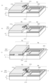
- FIG. 1A to 1C are diagrams illustrating a first example of a procedure for fabricating an integrated circuit 1.
- 1A to 1C are diagrams illustrating a procedure for producing a short gate length transistor.
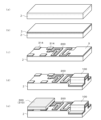
- 11A to 11C are diagrams illustrating a second example of a procedure for manufacturing the integrated circuit 1.
- FIG. 1 is a schematic diagram showing the structure of an integrated circuit 1 according to an embodiment of the present invention.
- the integrated circuit 1 has a structure in which a first region R1, a second region R2, and a third region R3 are provided on a substrate 2.
- the first region R1 is a region in which a short gate length transistor 100 is formed.
- the second region R2 is a region in which an antenna element 200 is formed.
- the third region R3 is a region in which a gallium nitride device 310 is formed.
- the integrated circuit 1 has a short gate length transistor 100, an antenna element 200, and a GaN device 310 formed on one substrate.
- the short gate length transistor 100, the antenna element 200, and the GaN device 310 on the substrate 2 are connected to each other as necessary to achieve the required functions.
- At least the top surface 21 of the substrate 2 is made of single-crystal silicon carbide.
- the top surface 21 is the top flat surface of the substrate 2.
- the portion of the substrate 2 other than the top surface may be an insulator other than silicon carbide.
- the substrate 2 may be a single-crystal substrate of silicon carbide, or a hybrid substrate in which a single-crystal layer of silicon carbide is fabricated on an insulator.
- the surface of the single-crystal layer of silicon carbide in the substrate 2 may be the (0001) plane.
- the substrate 2 serves as a base for epitaxially growing the graphene that constitutes the graphene layer 3.
- the graphene layer 3 is a thin film of graphene of a single atomic layer or several atomic layers formed in contact with the top surface 21 of the substrate 2.
- the graphene that constitutes the graphene layer 3 can be formed into a single-layer thin film on the (0001) plane of silicon carbide, which is suitable for the substrate 2.
- the short gate length transistor 100 is configured to include a graphene layer 3, a shielding layer 4, an insulating layer 5, an insulating film 6, a two-dimensional semiconductor layer 7, an electrode 8, and an electrode 9 on a substrate 2.
- a vertical surface 22 and a lower surface 23 are formed on the substrate 2 by digging down from the top surface 21.
- the vertical surface 22 is a plane that intersects with the top surface 21 and extends downward from the top surface 21. In the example of FIG. 2, the vertical surface 22 and the top surface 21 are perpendicular to each other.
- the lower surface 23 is formed as a plane that is approximately parallel to the top surface 21 and intersects with the vertical surface 22.
- the lower surface 23 and the vertical surface 22 are perpendicular to each other, and the top surface 21 and the lower surface 23 are parallel to each other.
- the vertical surface 22 is formed as a plane that intersects with the top surface 21 and the lower surface 23.
- the thickness of the graphene layer 3 in the short gate length transistor 100 formed in the first region R1 is set to about several nm or less.
- the width from one end of the graphene layer 3 to the other end (horizontal direction in FIG. 2) may be about 100 nm to 1 ⁇ m.
- the graphene layer 3 is provided so as to cover the top surface 21 up to the vicinity of the ridge where the top surface 21 and the vertical surface 22 of the substrate 2 intersect.
- An end (edge) 31 of the graphene layer 3 that overlaps the vicinity of the ridge where the top surface 21 and the vertical surface 22 intersect functions as a gate in the short gate length transistor 100.
- the portion of the graphene layer 3 other than the edge 31 functions as wiring to the gate described later.
- the shielding layer 4 is a layer of a conductor such as a metal provided on the graphene layer 3, and shields between the electrode 8 and the graphene layer 3.
- the shielding layer 4 is electrically connected to a predetermined ground potential (e.g., 0 V).
- An insulating layer 5 is provided on at least the front and back sides of the shielding layer 4 to prevent the shielding layer 4 from shorting with the graphene layer 3 or the electrode 8. It is preferable to use aluminum (Al) or nickel (Ni) as the shielding layer 4.
- Al aluminum
- Ni nickel
- the shielding layer 4 When Ni is used as the shielding layer 4, it is necessary to form a separate insulating layer 5 to prevent shorting with the graphene layer 3 or the electrode 8. Note that when there is no need to shield between the electrode 8 and the graphene layer 3 (for example, when signal interference between the electrode 8 and the graphene layer 3 is not a problem), the shielding layer 4 and the insulating layer 5 may not be provided.
- the end surface 51 of the insulating layer 5 should be a flat surface that is approximately aligned with the vertical surface 22.
- the insulating film 6 is a thin film of an insulator that functions as a gate insulating film of the short gate length transistor 100.
- a high dielectric constant insulating film such as hafnium oxide, silicon carbide, zirconium oxide, erbium oxide, aluminum oxide, etc.
- a thin film of silicon carbide, etc. can be used.
- a thin film of silicon carbide is suitable.
- the insulating film 6 is formed so as to cover the upper surface of the insulating layer 5 through the end surface 51, the edge 31, the vertical surface 22, and the lower surface 23.
- the insulating film 6 covers at least the vertical surface 22, the edge 31, and the end surface 51 of the substrate 2, there are cases where it is not necessary to form the insulating film 6 on other parts.
- the insulating film 6 does not need to be provided on the insulating layer 5.
- the substrate 2 has sufficient insulating properties, it is not necessary to provide an insulating film 6 on the lower surface 23.
- the two-dimensional semiconductor layer 7 is a semiconductor layer that functions as a carrier transport layer of the short gate length transistor 100.
- the two-dimensional semiconductor layer 7 is formed so as to cover the top surface 21, the vertical surface 22, and the lower surface 23. In places where the graphene layer 3, the shielding layer 4, the insulating layer 5, and/or the insulating film 6 are present, the two-dimensional semiconductor layer 7 is formed so as to cover them as well.
- transition metal dichalcogenide e.g., molybdenum disulfide (MoS 2 ), tungsten disulfide (WS 2 ), tungsten diselenide (WSe 2 ), etc.
- MoS 2 molybdenum disulfide
- WS 2 tungsten disulfide
- WSe 2 tungsten diselenide
- indium oxide In 2 O 3
- boron phosphide boron arsenide, etc.
- graphene is suitable as the two-dimensional semiconductor layer 7.
- transition metal dichalcogenides such as MoS 2 and WS 2 are suitable for the two-dimensional semiconductor layer 7.
- In 2 O 3 and transition metal dichalcogenides are suitable for the two-dimensional semiconductor layer 7.
- Electrode 8 and electrode 9 are electrodes made of metals such as Au, Al, In, Bi, Ni, Pd, Ti, and Pt, or transparent conductive oxides such as ITO and FTO. Electrode 8 is provided overlapping a portion of the two-dimensional semiconductor layer 7 that covers the graphene layer 3, and functions as a source electrode of the short gate length transistor 100. Electrode 9 is provided overlapping a portion of the two-dimensional semiconductor layer 7 that covers the lower surface 23, and functions as a drain electrode of the short gate length transistor 100.
- the formation surface of the graphene layer 3 and the formation surface of the two-dimensional semiconductor layer 7 covering the vertical surface 22 are perpendicular to each other, and the edge 31 of the graphene layer 3 faces the two-dimensional semiconductor layer 7 via the insulating film 6, so that the thickness of the graphene layer 3 defines the gate length of the transistor 1.
- the gate length of the short gate length transistor 100 can be shortened to 0.3 nm. Even if the graphene layer 3 is a multilayer film of graphene, a gate length of several nm or less corresponding to the thickness of the graphene layer 3 can be realized.
- the short gate length transistor formed in the first region R1 may have a structure shown in FIG. 3 in order to suppress the gate resistance while realizing a gate length of a monoatomic layer.
- FIG. 3 is a cross-sectional view showing the structure of a short gate length transistor 100a according to a modified example.
- the short gate length transistor 100a like the above-mentioned short gate length transistor 100, has a graphene layer 3, a shielding layer 4, an insulating layer 5, an insulating film 6, a two-dimensional semiconductor layer 7, an electrode 8, and an electrode 9 in the first region R1 of the substrate 2.
- the first region R1 of the substrate 2 has a top surface 21, a vertical surface 22, a lower surface 23, and a slope 24.
- the top surface 21 and the slope 24 are single crystals of silicon carbide.
- the slope 24 is a non-parallel (inclined) surface to the top surface 21 that is provided adjacent to the top surface 21 at the end opposite to the edge of the top surface 21 that contacts the vertical surface 22.
- the inclination angle of the inclined surface 24 is arbitrary, and may be, for example, 45°, 22°, etc.
- the inclination angle of the inclined surface 24 does not need to be constant, and may be, for example, a curved surface.
- Such an inclined surface 24 is provided prior to the formation of the graphene layer 3. In the short gate length transistor 100a, the graphene layer 3 is simultaneously formed from the top surface 21 to the inclined surface 24.
- the growth rate of graphene on the inclined surface 24 is faster than the growth rate of graphene on the top surface 21, which is the (0001) plane of silicon carbide, multiple layers of graphene (preferably about 10 to 20 layers) grow on the inclined surface 24 while a single layer of graphene is grown on the top surface 21. Therefore, the graphene layer 3 in the short gate length transistor 100a is formed from the top surface 21 to the slope 24, and has a structure in which the vicinity of the edge 31 is a single-layer graphene 32, while on the inner slope 24 it switches to a multi-layer graphene 33.
- the distance from the ridge where the top surface 21 and the vertical surface 22 of the substrate 2 intersect to the slope 24 is preferably a sufficient distance (e.g., about several hundreds of nm) to prevent the formation of the multi-layer graphene from extending to the vicinity of the edge 31.
- the short gate length transistor 100a is constructed by providing the graphene layer 3 as described above with a shielding layer 4, insulating layer 5, insulating film 6, two-dimensional semiconductor layer 7, electrode 8, and electrode 9 similar to those of the short gate length transistor 100. Note that due to the inclination of the underlying slope 24, a depression will form in the graphene layer 3 at the slope 24, but it is advisable to fill this depression with an insulating material or the like to make a flat surface before stacking the shielding layer 4, insulating film 6, two-dimensional semiconductor layer 7, etc.
- the carrier density increases due to the multi-layering of the graphene layer 3, so that the resistance of the graphene layer 3 as a whole can be reduced.
- a single layer of graphene faces the two-dimensional semiconductor layer 7 via the insulating film 6 and functions as a gate electrode, so that the gate length of the transistor 1 can be one atom (about 0.3 nm).
- the graphene layer 3 is patterned into a desired shape as shown in FIG. 1 to form the antenna element 200 and the connection portion 210.
- the antenna element 200 has a structure in which the graphene layer 3 is patterned into a shape for achieving desired antenna characteristics.
- a metal film such as Au or a protective film such as an insulator may be provided by superimposing a part or all of the patterned graphene.
- graphene Compared with metals such as copper (Cu) and ITO, graphene has high values of various properties such as electrical conductivity, carrier mobility, and thermal conductivity, so that it is possible to achieve antenna characteristics superior to those of Cu, and characteristic deterioration can be suppressed even if the size of the antenna is reduced.
- the graphene layer 3 forming the antenna element 200 in the second region R2 and the graphene layer 3 forming the gate of the short gate length transistor 100 in the first region R1 are preferably formed as a continuous graphene film.
- the gate of the short gate length transistor 100 and the antenna element 200 are preferably electrically connected to each other using the graphene layer 3 as wiring. In this way, the length of the wiring connecting the gate of the short gate length transistor 100 and the antenna element 200 can be made extremely short.
- the connection part 210 is a wiring that connects the electrode 312 of the amplifier of the GaN device 310 described later and the antenna element 200.
- the connection part 210 may not be provided with the GaN layer 300 described later, or the GaN layer 300 may be provided over a part or all of the connection part 210.
- the connection part 210 may be formed by patterning the graphene layer 3, or may be formed with a metal film such as Au. Also, the connection part 210 may be partially formed with a metal film and other parts with graphene, or may have a part where a metal film is provided over the graphene. If the antenna element 200 and the connection part 210 are formed only with graphene, transparent wiring can be realized.
- connection part 210 is formed as short as possible (for example, so that the transmission distance is preferably less than 100 ⁇ m, more preferably less than 30 ⁇ m, and even more preferably less than 10 ⁇ m) so that the signal transmitted between the GaN device 310 and the antenna element 200 is not deteriorated.
- a gallium nitride layer 300 is laminated on the substrate 2.
- the gallium nitride layer 300 is provided on top of the graphene layer 3 as shown in FIG. 4(a).
- the graphene layer 3 functions as a buffer layer for relieving stress between the substrate 2 and the GaN layer 300.
- the gallium nitride layer 300 may be provided directly on the substrate 2 without the graphene layer 3.
- a gallium nitride device 310 which is an active element such as an amplifier, is formed using an element capable of high-speed operation such as a high electron mobility transistor (HEMT).
- HEMT high electron mobility transistor
- a metal film e.g., an Au film
- a protective film, etc. may be provided on top of the graphene layer 3 or the gallium nitride layer 300 as necessary.
- the gallium nitride device 310 may include other active elements in addition to the amplifier described above.
- the gallium nitride device 310 may include an electrode 312 to which wiring from the outside (e.g., the antenna element 200 or the connection portion 210) is connected.
- the electrode 312 may be provided on the surface of the gallium nitride layer 300 facing the substrate 2, or on the surface opposite to the surface facing the substrate 2.
- the electrode 312 and an electrode pad 314 provided at one end of the connection part 210 may be connected directly or indirectly via a conductor, as shown in FIG. 4(c).
- the electrode 312 When the electrode 312 is provided on the surface of the gallium nitride layer 300 opposite the surface facing the substrate 2, the electrode 312 and the connection part 210 may be connected by wire bonding 316, as shown in FIG. 4(a) or FIG. 4(b). Alternatively, the electrode 312 and the connection part 210 may be connected by adding a conductor layer 318 such as metal or graphene, as shown in FIG. 4(d).
- a gallium nitride device 310 may be prepared separately, and the gallium nitride device 310 may be bonded to the third region R3 of the substrate 2 on which the graphene layer 3 is provided, thereby providing the gallium nitride layer 300.
- the structure shown in FIG. 5(c) corresponds to the configuration of this modification.
- the integrated circuit 1 achieves the desired functionality by arranging the first region R1, second region R2, and third region R3 described above, as well as other necessary circuit elements, in any combination on the substrate 2.
- Figure 5 shows a first example of the procedure for manufacturing the integrated circuit 1.
- a substrate 2 is prepared (FIG. 5(a)).
- the top surface of the substrate 2 is made of single crystal silicon carbide.
- the crystal structure of the silicon carbide on the top surface is preferably 4H-SiC, 6H-SiC, or 3C-SiC.
- one of single crystal silicon, sapphire, polycrystalline silicon, alumina, silicon nitride, aluminum nitride, diamond, or polycrystalline silicon carbide is used as a base substrate, on which a film of silicon oxide, single crystal silicon, polycrystalline silicon, amorphous silicon, alumina, silicon nitride, silicon carbide, aluminum nitride, or diamond is provided as necessary, and the bonding surfaces of the base substrate and silicon carbide substrate are subjected to a surface treatment before bonding.
- a hybrid substrate in which the single crystal layer of silicon carbide is thinned can be produced by an ion implantation peeling method in which hydrogen ions, helium ions, etc. are implanted into the silicon carbide substrate before thinning by grinding and polishing or peeling, and peeling is performed at the ion implantation interface by heat treatment after bonding.
- the surface can be subjected to CVD with polycrystalline silicon carbide, and then the base substrate can be removed to obtain a hybrid substrate in which a single crystal layer of silicon carbide is produced on the insulator.
- a slope 24 is formed at the location where the short gate length transistor 100a is to be formed.
- the substrate 2 is heated to preferably 1,100° C. or higher to sublimate silicon atoms (Si) near the top surface 21 (and the inclined surface 24) of the substrate 2, thereby forming a graphene film of a desired thickness (for example, about 50 to 1,500 nm) to form the graphene layer 3 (FIG. 5B).
- Si silicon atoms
- FIG. 5B graphene layer 3
- heating is performed for 5 to 30 minutes under an argon (Ar) atmosphere at a pressure of 10 5 Pa (1 bar) and a temperature of 1500 to 1600° C.
- Ar argon
- a nanocarbon film of any of fullerene, graphene, and carbon nanotubes is formed, and the preparation conditions are appropriately adjusted so that graphene is obtained.
- the graphene layer 3 thus formed grows epitaxially so that the crystals are oriented in a predetermined direction with respect to the crystal plane of the silicon carbide single crystal on the top surface of the substrate 2, which serves as the base.
- gallium nitride is epitaxially grown using the graphene layer 3 as a buffer layer (i.e., a nucleation layer (template layer) of gallium nitride epicrystal) to form a gallium nitride layer 300 (FIG. 5(c)).
- Gallium nitride may be epitaxially grown, for example, by metalorganic chemical vapor deposition (MOCVD). Specifically, trimethylgallium (TMGa), trimethylaluminum (TMAl), and ammonia (NH 3 ) may be used as precursors of Ga, Al, and N, respectively, and H 2 and N 2 may be used as carrier gases.
- MOCVD metalorganic chemical vapor deposition
- the substrate 2 provided with the graphene layer 3 may be thermally cleaned in an H 2 atmosphere at 1100° C. for about 5 minutes.
- An AlN buffer layer may be grown to a thickness of about 10 to 100 nm on the substrate surface after cleaning, and then an undoped gallium nitride layer 300 having a thickness of about 2 ⁇ m may be grown at 1050° C.
- the AlN buffer layer may be grown such that a high-temperature AlN buffer layer grown at about 1080° C. is laminated on a low-temperature AlN buffer layer grown at about 780° C.
- the graphene layer 3 is used as a nucleation layer (template layer) for the gallium nitride epitaxial crystal, but before the growth of the gallium nitride epitaxial crystal, the graphene layer 3 may be removed from the portion where the gallium nitride is to be grown (i.e., the portion where the active element portion is provided), and gallium nitride may be grown directly on the silicon carbide single crystal on the uppermost surface 21 of the substrate 2.
- active elements such as HEMTs, passive elements such as resistors, capacitors, and inductors, wiring, electrodes, etc. are formed on the formed gallium nitride layer 300 to form a gallium nitride device 310 including an amplifier, etc. ( Figure 5 (d)).
- the gallium nitride layer 300 is removed by etching from the portions other than the gallium nitride device 310, exposing the graphene layer 3 in the regions that will become the first region R1 and the second region R2 (FIG. 5(e)). Furthermore, the antenna element 200 and the connection portion 210 are patterned on the graphene layer 3 (FIG. 5(f)). Note that when patterning the graphene layer 3, the graphene layer 3 is left in the region that will become the first region R1.
- This patterning may be performed, for example, by evaporating an Au film on the graphene layer 3, patterning the Au film using photolithography and etching techniques, removing the exposed graphene that is not covered with the Au film using UV-ozone treatment or the like, and then removing unnecessary portions of the Au film.
- a short gate length transistor 100 or 100a is formed in the region that will become the first region R1 (FIG. 5(g)).
- a shielding layer 4 of Al is formed in the region that will become the first region R1 where the graphene layer 3 is exposed.
- an insulating layer 5 of a natural oxide film is formed on the shielding layer 4 so as to cover its surface (FIG. 6(a)).
- the shielding layer 4 when a material that does not form a natural oxide film other than Al is used as the shielding layer 4, it is preferable to form insulating layers above and below the shielding layer 4 to ensure insulation between the shielding layer 4 and the graphene 3 or the electrode 8.
- a part of the first region R1 of the substrate 2 is dug down to form a vertical surface 22 and a lower surface 23 on the substrate 2, and the shielding layer 4 is processed to match the vertical surface 22 (FIG. 6(b)).
- the side surface of the shielding layer 4 is exposed, and the insulating layer 5 of the natural oxide film is formed again to cover the exposed surface.
- the graphene layer 3 is not present on the vertical surface 22 and the lower surface 23 formed by microfabrication, but a single layer of the graphene layer 3 is left on the remaining top surface 21.
- the insulating film 6 is deposited (FIG. 6C). In FIG. 6C, the insulating film 6 is formed so as to cover the upper surface of the insulating layer 5, the end surface 51, the edge 31, the vertical surface 22, and the lower surface 23. Note that the insulating film 6 may not be formed on other parts as long as it covers at least the vertical surface 22, the edge 31, and the end surface 51 of the substrate 2.
- the two-dimensional semiconductor layer 7 is deposited so as to cover the top surface 21, the vertical surface 22, and the lower surface 23 (FIG. 6D).
- the two-dimensional semiconductor layer 7 is formed so as to cover the graphene layer 3, the shielding layer 4, the insulating layer 5, and/or the insulating film 6 at locations where they are present.
- an electrode 8 is formed so as to cover the graphene layer 3 in the two-dimensional semiconductor layer 7, and an electrode 9 is formed so as to cover the lower surface 23 in the two-dimensional semiconductor layer 7 (FIG. 6(e)).
- the structure of the short gate length transistor 100 is thus completed.
- the first region R1, the second region R2, and the third region R3 are interconnected (e.g., the connection between the electrode 312 of the gallium nitride device 310 and the connection portion 210) and electrode pads for connection to the outside (e.g., pads for connecting to the source electrode, drain electrode, and gate electrode of the short gate length transistor 100) are formed, thereby obtaining the integrated circuit 1 (FIG. 5(h)).
- a monolithic integrated circuit 1 can be fabricated in which a short gate length transistor, an antenna element, and a gallium nitride device are provided on a substrate 2.
- the order of the formation of the short gate length transistor, the antenna element, and the gallium nitride device may be reversed, or some or all of the steps may be performed simultaneously.
- the integrated circuit 1 created as described above has the antenna element 200 and the short gate length transistor 100 arranged in close proximity and connected by a continuous graphene layer 3, so signal degradation can be suppressed even in signal frequency bands of 1 THz or more.
- the short gate length transistor 100 and the gallium nitride device 310 can be formed on the same substrate, making it possible to cover a wide range of signal frequency bands from several tens of GHz to over 100 GHz, up to over 1 THz.
- FIG. 7 is a diagram showing a second example of the procedure for fabricating an integrated circuit 1. This procedure differs from the first example in that the gallium nitride layer 300 is not epitaxially grown, but a gallium nitride device 310 is separately prepared, and the gallium nitride layer is provided by bonding the gallium nitride device 310 to a substrate 2 on which a graphene layer 3 is provided.
- a substrate 2 is prepared (FIG. 7(a)) by a method similar to that described with reference to FIGS. 5(a) and 5(b) and, if necessary, a slope 24 is formed, followed by the formation of a graphene layer 3 (FIG. 7(b)).
- the antenna element 200 and the connection portion 210 are patterned on the graphene layer 3 (FIG. 7(c)).
- the electrode pad 314 connected to the electrode 312 of the integrated circuit is also patterned in a form extending from the connection portion 210.
- the graphene layer 3 is left in the region that will become the first region R1.
- a pattern of the graphene layer 3 (or the Au film provided thereon) required for bonding with the gallium nitride device 310 may be formed.
- the graphene layer 3 may function as an adhesive layer for attaching the gallium nitride device 310 to the substrate 2.
- these patternings may be performed in the following procedure: an Au film is vapor-deposited on the graphene layer 3, and then the Au film is patterned by photolithography and etching techniques, the exposed graphene not covered with the Au film is removed by UV-ozone treatment or the like, and the unnecessary parts of the Au film are further removed.
- the antenna element 200 can be monolithically formed on the substrate 2.
- the pattern used for bonding to the gallium nitride device 310 may be formed only of a metal thin film such as Au after removing the graphene layer 3.
- the pattern used for bonding to the gallium nitride device 310 may be made of graphene, a metal thin film, or a laminate of these.
- the pattern used for bonding to the gallium nitride device 310 may also function to ensure electrical connection between the elements in the gallium nitride device 310 and the outside, similar to the electrode pad 314 connected to the electrode 312.
- a short gate length transistor 100 or 100a is formed in the first region R1 using a method similar to that described with reference to FIG. 7 (FIG. 7(d)).
- a gallium nitride device 310 prepared separately is attached to an appropriate position in the third region R3 of the substrate 2 (FIG. 7(e)).
- the gallium nitride device 310 is formed by forming active elements such as amplifiers on a gallium nitride substrate and cutting it to a predetermined size.
- the surface of the gallium nitride device 310 (the surface that is attached to the substrate 2) is provided with electrodes 312 for transmitting and receiving signals.
- the electrodes 312 of the gallium nitride device 310 and the electrode pads 314 on the substrate 2 are electrically connected.
- the gallium nitride device 310 and the substrate 2 may be attached to each other after performing an activation process or a surface treatment on the surfaces of both of them.
- the gallium nitride device 310 may also be attached to the substrate 2 by flip-chip bonding.
- the gallium nitride device 310 attached to the substrate 2 becomes the gallium nitride layer 300 in the integrated circuit 1.
- a monolithic integrated circuit 1 can be fabricated that includes a short gate length transistor, an antenna element, and a gallium nitride device on a substrate 2.
- the integrated circuit 1 created as described above has the antenna element 200 and the short gate length transistor 100 arranged in close proximity and connected by a continuous graphene layer 3, so signal degradation can be suppressed even in signal frequency bands of 1 THz or more.
- the short gate length transistor 100 and the gallium nitride device 310 can be formed on the same substrate, making it possible to cover a wide range of signal frequency bands from several tens of GHz to over 100 GHz, up to over 1 THz.
- the gallium nitride device 310 can be prepared separately and then bonded to the substrate 2, allowing for high design freedom in the gallium nitride device. Furthermore, by preparing multiple types of gallium nitride devices 310 with different functions and performance to be bonded together, it is possible to create integrated circuits 1 with a wide variety of third region R3 variations while keeping the first region R1 and second region R2 common.
Landscapes
- Thin Film Transistor (AREA)
- Junction Field-Effect Transistors (AREA)
Abstract
Description
2 基板
21 最上面
22 垂直面
23 下段面
24 斜面
3 グラフェン層
31 エッジ
4 遮蔽層
5 絶縁層
51 端面
6 絶縁膜
7 二次元半導体層
8,9 電極
100,100a 短ゲート長トランジスタ
200 アンテナエレメント
300 窒化ガリウム層
310 窒化ガリウムデバイス
318 導体層
R1 第1領域
R2 第2領域
R3 第3領域
Claims (20)
- 少なくとも最上面が炭化珪素の単結晶であり、前記最上面と交わり前記最上面より下方に延びる垂直面と、前記最上面と略平行であり前記垂直面と交わる下段面とを有する基板と、
前記基板の最上面に接して設けられた単結晶のグラフェン層と、
を備え、
短ゲート長トランジスタとアンテナエレメントとが一体的に形成された集積回路であって、
前記短ゲート長トランジスタは、
前記グラフェン層が前記垂直面と交わる端部をゲート電極とし、
少なくとも、前記垂直面、前記グラフェン層の前記端部を覆うように形成される絶縁膜と、
前記最上面、前記垂直面、および前記下段面を覆うように形成される二次元半導体層であって、前記グラフェン層および/または前記絶縁膜が存在する箇所については前記グラフェン層および/または前記絶縁膜をも覆うように重ねて形成される、二次元半導体層と、
前記二次元半導体層における前記最上面を覆う箇所に設けられるソース電極と、
前記二次元半導体層における前記下段面を覆う箇所に設けられるドレイン電極とを備え、
前記アンテナエレメントは、前記グラフェン層をパターニングにして形成される、
集積回路。 - 前記グラフェン層において、前記短ゲート長トランジスタにおけるゲート電極を成す部分と前記アンテナエレメントを成す部分とは連続したグラフェンの膜として形成されることを特徴とする請求項1に記載の集積回路。
- 前記基板上における、前記短ゲート長トランジスタおよび前記アンテナエレメントが設けられていない領域に、窒化ガリウム層をさらに備え、
前記窒化ガリウム層にアクティブ素子が形成されたことを特徴とする請求項1に記載の集積回路。 - 少なくとも最上面が炭化珪素の単結晶であり、前記最上面と交わり前記最上面より下方に延びる垂直面と、前記最上面と略平行であり前記垂直面と交わる下段面とを有する基板と、
前記基板の最上面に接して設けられた単結晶のグラフェン層と、
前記基板上に設けられた窒化ガリウム層と、
を備え、
前記窒化ガリウム層に形成されたアクティブ素子部と、前記グラフェン層をゲートとして用いる短ゲート長トランジスタとが一体的に形成された集積回路であって、
前記短ゲート長トランジスタは、
前記グラフェン層が前記垂直面と交わる端部をゲート電極とし、
少なくとも、前記垂直面、前記グラフェン層の前記端部を覆うように形成される絶縁膜と、
前記最上面、前記垂直面、および前記下段面を覆うように形成される二次元半導体層であって、前記グラフェン層および/または前記絶縁膜が存在する箇所については前記グラフェン層および/または前記絶縁膜をも覆うように重ねて形成される、二次元半導体層と、
前記二次元半導体層における前記最上面を覆う箇所に設けられるソース電極と、
前記二次元半導体層における前記下段面を覆う箇所に設けられるドレイン電極とを備える、集積回路。 - 前記短ゲート長トランジスタは、
ゲートを成す前記グラフェン層の上に、導体の遮蔽層をさらに備え、
前記遮蔽層の表裏両面に絶縁層が設けられる
ことを特徴とする請求項1から4の何れか1項に記載の集積回路。 - 前記グラフェン層は、少なくとも、前記端部が単原子層のグラフェンであることを特徴とする請求項1から4の何れか1項に記載の集積回路。
- 前記基板は、前記最上面と前記垂直面とが接する縁から離れた位置に前記最上面と非平行である斜面を備え、
前記グラフェン層は前記最上面から前記斜面に渡って形成され、
前記斜面の上における前記グラフェン層は多層のグラフェンである
ことを特徴とする請求項6に記載の集積回路。 - 前記基板は、絶縁体のベース基板上に炭化珪素の単結晶層を作製したハイブリッド基板であることを特徴とする、請求項1から4の何れか1項に記載の集積回路。
- 前記窒化ガリウム層は、前記グラフェン層の一部を覆うように設けられることを特徴とする請求項3または4に記載の集積回路。
- 前記窒化ガリウム層は、前記グラフェン層をバッファ層としてエピタキシャル成長された層であることを特徴とする請求項9に記載の集積回路。
- 前記窒化ガリウム層に形成されるアクティブ素子はHEMT(High Electron Mobility Transistor)を用いた増幅器を含むことを特徴とする請求項3または4に記載の集積回路。
- 短ゲート長トランジスタとアンテナエレメントとが一体的に形成された集積回路の製造方法であって、
少なくとも最上面が炭化珪素の単結晶である基板を用意するステップと、
前記基板の最上面にグラフェン層を形成するステップと、
前記短ゲート長トランジスタが形成される前記基板の第1領域において、
微細加工により、一部に前記グラフェン層を残しつつ、他の部分について前記グラフェン層および前記基板の上部を除去して、前記基板に、前記最上面と交わり前記最上面より下方に延びる垂直面と、前記最上面と略平行であり前記垂直面と交わる下段面垂直面および下段面とを形成するステップと、
少なくとも、前記垂直面および前記グラフェン層の端部を覆うように絶縁膜を堆積するステップと、
前記最上面、前記垂直面、および前記下段面を覆うように、且つ、前記グラフェン層および/または前記絶縁膜が存在する箇所については前記グラフェン層および/または前記絶縁膜をも覆うように重ねて二次元半導体層を堆積するステップと、
前記二次元半導体層における前記グラフェン層を覆う箇所に重ねてソース電極を形成し、前記二次元半導体層における前記下段面を覆う箇所に重ねてドレイン電極を形成するステップと、
前記アンテナエレメントが形成される前記基板の第2領域において、前記グラフェン層をパターニングしてアンテナエレメントを形成するステップと、
を含む、集積回路の製造方法。 - 前記グラフェン層をバッファ層として窒化ガリウム層をエピタキシャル成長するステップと、
前記第1領域および前記第2領域において、前記窒化ガリウム層を除去して前記グラフェン層を露出させるステップと、
残存する前記窒化ガリウム層に増幅器を含むアクティブ素子部を形成するステップと、
をさらに備えることを特徴とする請求項12に記載の集積回路の製造方法。 - 前記グラフェン層の一部を除去するステップと、
前記グラフェン層が除去された領域に、窒化ガリウム層をエピタキシャル成長するステップと、
前記窒化ガリウム層に増幅器を含むアクティブ素子部を形成するステップと、
をさらに備え、
前記第1領域および前記第2領域は、前記グラフェン層が残存する領域に設けられることを特徴とする請求項12に記載の集積回路の製造方法。 - 短ゲート長トランジスタと窒化ガリウム層に形成されるアクティブ素子とが一体的に形成された集積回路の製造方法であって、
少なくとも最上面が炭化珪素の単結晶である基板を用意するステップと、
前記基板の最上面にグラフェン層を形成するステップと、
前記グラフェン層をバッファ層として窒化ガリウム層をエピタキシャル成長するステップと、
前記短ゲート長トランジスタが形成される前記基板の第1領域において、
前記窒化ガリウム層を除去して前記グラフェン層を露出させるステップと、
微細加工により、一部に前記グラフェン層を残しつつ、他の部分について前記グラフェン層および前記基板の上部を除去して、前記基板に、前記最上面と交わり前記最上面より下方に延びる垂直面と、前記最上面と略平行であり前記垂直面と交わる下段面垂直面および下段面とを形成するステップと、
少なくとも、前記垂直面および前記グラフェン層の端部を覆うように絶縁膜を堆積するステップと、
前記最上面、前記垂直面、および前記下段面を覆うように、且つ、前記グラフェン層および/または前記絶縁膜が存在する箇所については前記グラフェン層および/または前記絶縁膜をも覆うように重ねて二次元半導体層を堆積するステップと、
前記二次元半導体層における前記グラフェン層を覆う箇所に重ねてソース電極を形成し、前記二次元半導体層における前記下段面を覆う箇所に重ねてドレイン電極を形成するステップと、
残存する前記窒化ガリウム層に増幅器を含むアクティブ素子部を形成するステップと、
と、
を含む、集積回路の製造方法。 - 短ゲート長トランジスタと窒化ガリウム層に形成されるアクティブ素子とが一体的に形成された集積回路の製造方法であって、
少なくとも最上面が炭化珪素の単結晶である基板を用意するステップと、
前記基板の最上面にグラフェン層を形成するステップと、
前記グラフェン層の一部を除去するステップと、
前記グラフェン層が除去された領域に、窒化ガリウム層をエピタキシャル成長するステップと、
前記窒化ガリウム層に増幅器を含むアクティブ素子部を形成するステップと、
前記グラフェン層が残存する領域において、
微細加工により、一部に前記グラフェン層を残しつつ、他の部分について前記グラフェン層および前記基板の上部を除去して、前記基板に、前記最上面と交わり前記最上面より下方に延びる垂直面と、前記最上面と略平行であり前記垂直面と交わる下段面垂直面および下段面とを形成するステップと、
少なくとも、前記垂直面および前記グラフェン層の端部を覆うように絶縁膜を堆積するステップと、
前記最上面、前記垂直面、および前記下段面を覆うように、且つ、前記グラフェン層および/または前記絶縁膜が存在する箇所については前記グラフェン層および/または前記絶縁膜をも覆うように重ねて二次元半導体層を堆積するステップと、
前記二次元半導体層における前記グラフェン層を覆う箇所に重ねてソース電極を形成し、前記二次元半導体層における前記下段面を覆う箇所に重ねてドレイン電極を形成するステップと、
を含む、集積回路の製造方法。 - 増幅器を含むアクティブ素子部が形成された窒化ガリウムデバイスを、前記基板上の前記グラフェン層に貼り合わせて窒化ガリウム層を設けるステップと、
を含む、請求項12に記載の集積回路の製造方法。 - 前記アンテナエレメントを形成するステップにおいて、前記アンテナエレメントとともに、電極パッドおよび前記アンテナエレメントと前記電極パッドとを接続する接続部を形成し、
前記窒化ガリウム層を設けるステップにおいて、前記窒化ガリウムデバイスに設けられた電極と、前記電極パッドとが電気的に接続されるように、前記窒化ガリウムデバイスを前記基板上の前記グラフェン層に貼り合わせることを特徴とする請求項17に記載の集積回路の製造方法。 - 前記グラフェン層を形成するステップにおいて、前記基板の最上面の炭化珪素の単結晶における珪素原子を昇華させることによりグラフェン層をエピタキシャル成長させることを特徴とする請求項12から18の何れか1項に記載の集積回路の製造方法。
- 前記基板は、絶縁体のベース基板上に炭化珪素の単結晶層を作製したハイブリッド基板であることを特徴とする、請求項12から18の何れか1項に記載の集積回路の製造方法。
Priority Applications (3)
| Application Number | Priority Date | Filing Date | Title |
|---|---|---|---|
| KR1020257040637A KR20260021624A (ko) | 2023-06-09 | 2024-04-18 | 집적 회로 및 그의 제조 방법 |
| CN202480037755.0A CN121312278A (zh) | 2023-06-09 | 2024-04-18 | 集成电路及其制造方法 |
| EP24819038.1A EP4726781A1 (en) | 2023-06-09 | 2024-04-18 | Integrated circuit and method for manufacturing same |
Applications Claiming Priority (2)
| Application Number | Priority Date | Filing Date | Title |
|---|---|---|---|
| JP2023-095712 | 2023-06-09 | ||
| JP2023095712A JP2024176869A (ja) | 2023-06-09 | 2023-06-09 | 集積回路及びその製造方法 |
Publications (1)
| Publication Number | Publication Date |
|---|---|
| WO2024252800A1 true WO2024252800A1 (ja) | 2024-12-12 |
Family
ID=93795397
Family Applications (1)
| Application Number | Title | Priority Date | Filing Date |
|---|---|---|---|
| PCT/JP2024/015407 Ceased WO2024252800A1 (ja) | 2023-06-09 | 2024-04-18 | 集積回路及びその製造方法 |
Country Status (6)
| Country | Link |
|---|---|
| EP (1) | EP4726781A1 (ja) |
| JP (1) | JP2024176869A (ja) |
| KR (1) | KR20260021624A (ja) |
| CN (1) | CN121312278A (ja) |
| TW (1) | TW202450076A (ja) |
| WO (1) | WO2024252800A1 (ja) |
Citations (5)
| Publication number | Priority date | Publication date | Assignee | Title |
|---|---|---|---|---|
| US20140158987A1 (en) * | 2012-12-06 | 2014-06-12 | Hrl Laboratories, Llc | Methods for integrating and forming optically transparent devices on surfaces |
| JP2016021456A (ja) * | 2014-07-14 | 2016-02-04 | 日本電信電話株式会社 | テラヘルツ帯用アンテナ |
| WO2018051739A1 (ja) * | 2016-09-13 | 2018-03-22 | ソニー株式会社 | 電磁波検出素子、電磁波センサ、電子機器及び構造体 |
| JP2019075626A (ja) | 2017-10-12 | 2019-05-16 | 晋二 黄 | マイクロ波帯アンテナ |
| WO2023119833A1 (ja) * | 2021-12-21 | 2023-06-29 | 国立大学法人東北大学 | アンテナモジュールおよびその製造方法 |
-
2023
- 2023-06-09 JP JP2023095712A patent/JP2024176869A/ja active Pending
-
2024
- 2024-04-18 CN CN202480037755.0A patent/CN121312278A/zh active Pending
- 2024-04-18 KR KR1020257040637A patent/KR20260021624A/ko active Pending
- 2024-04-18 WO PCT/JP2024/015407 patent/WO2024252800A1/ja not_active Ceased
- 2024-04-18 EP EP24819038.1A patent/EP4726781A1/en active Pending
- 2024-06-06 TW TW113121069A patent/TW202450076A/zh unknown
Patent Citations (5)
| Publication number | Priority date | Publication date | Assignee | Title |
|---|---|---|---|---|
| US20140158987A1 (en) * | 2012-12-06 | 2014-06-12 | Hrl Laboratories, Llc | Methods for integrating and forming optically transparent devices on surfaces |
| JP2016021456A (ja) * | 2014-07-14 | 2016-02-04 | 日本電信電話株式会社 | テラヘルツ帯用アンテナ |
| WO2018051739A1 (ja) * | 2016-09-13 | 2018-03-22 | ソニー株式会社 | 電磁波検出素子、電磁波センサ、電子機器及び構造体 |
| JP2019075626A (ja) | 2017-10-12 | 2019-05-16 | 晋二 黄 | マイクロ波帯アンテナ |
| WO2023119833A1 (ja) * | 2021-12-21 | 2023-06-29 | 国立大学法人東北大学 | アンテナモジュールおよびその製造方法 |
Non-Patent Citations (2)
| Title |
|---|
| FUKIDOME, HIROKAZU: "Creation of Affordable Manufacturing Processes of Ultrahigh-quality Graphene Growth and High-frequency Graphene Devices by Using Single-crystalline SiC Thin Films on Device-type Substrates", VACUUM AND SURFACE SCIENCE, vol. 64, no. 7, 2021, pages 318 - 323, XP093073274, DOI: 10.1380/vss.64.318 * |
| WU, FAN ET AL.: "Vertical MoS2 transistors with sub-1-nm gate lengths", NATURE, vol. 603, 9 March 2022 (2022-03-09), pages 259 - 264, XP037712043, DOI: 10.1038/s41586-021-04323-3 * |
Also Published As
| Publication number | Publication date |
|---|---|
| TW202450076A (zh) | 2024-12-16 |
| EP4726781A1 (en) | 2026-04-15 |
| JP2024176869A (ja) | 2024-12-19 |
| CN121312278A (zh) | 2026-01-09 |
| KR20260021624A (ko) | 2026-02-13 |
Similar Documents
| Publication | Publication Date | Title |
|---|---|---|
| JP5396784B2 (ja) | 半導体装置及びその製造方法 | |
| JP4339657B2 (ja) | 半導体装置及びその製造方法 | |
| TW546686B (en) | Mixed-signal semiconductor structure, device including the structure, and methods of forming the device and the structure | |
| JP7217808B2 (ja) | 半導体装置の製造方法 | |
| CN115708221B (zh) | 一种半导体器件及其制作方法、封装结构、电子设备 | |
| US9082817B2 (en) | Growth of multi-layer group III-nitride buffers on large-area silicon substrates and other substrates | |
| US20140159055A1 (en) | Substrates for semiconductor devices | |
| JP5216184B2 (ja) | 化合物半導体装置およびその製造方法 | |
| WO2022049983A1 (ja) | 半導体装置、半導体モジュール、及び無線通信装置 | |
| JP7765040B2 (ja) | アンテナモジュールおよびその製造方法 | |
| WO2024252800A1 (ja) | 集積回路及びその製造方法 | |
| KR20130008281A (ko) | 파워소자의 제조방법 | |
| JP2007142144A (ja) | 電界効果トランジスタ集積回路及びその製造方法 | |
| CN116762177A (zh) | 半导体结构及其制备方法、电子设备 | |
| CN116635995B (zh) | 半导体器件及其制备方法、电子设备 | |
| JP2019169544A (ja) | グラフェン含有構造体、半導体装置、およびグラフェン含有構造体の製造方法 | |
| JP5370441B2 (ja) | 窒化ガリウム系hemtの製造方法及び窒化ガリウム系hemt | |
| JP5464218B2 (ja) | 窒化ガリウム系hemtの製造方法及び窒化ガリウム系hemt | |
| KR20260020106A (ko) | 트랜지스터 및 그 제조 방법, 그리고 집적 회로 | |
| CN115985958A (zh) | 一种低欧姆接触GaN基高电子迁移率晶体管及其制备方法 | |
| CN115708222A (zh) | 一种半导体器件及其制作方法、封装结构、电子设备 | |
| CN118431263A (zh) | 含多层外延插入的外延片及制备方法、晶体管和射频器件 | |
| CN119997602A (zh) | 一种基于多材料复合基板构造的集成结构及其制作方法 | |
| CN121420650A (zh) | 氮化物半导体装置及其制造方法 | |
| CN119562565A (zh) | 半导体器件及其制备方法、芯片及电子设备 |
Legal Events
| Date | Code | Title | Description |
|---|---|---|---|
| 121 | Ep: the epo has been informed by wipo that ep was designated in this application |
Ref document number: 24819038 Country of ref document: EP Kind code of ref document: A1 |
|
| WWE | Wipo information: entry into national phase |
Ref document number: 2024819038 Country of ref document: EP |
|
| NENP | Non-entry into the national phase |
Ref country code: DE |
|
| ENP | Entry into the national phase |
Ref document number: 2024819038 Country of ref document: EP Effective date: 20260109 |
|
| ENP | Entry into the national phase |
Ref document number: 2024819038 Country of ref document: EP Effective date: 20260109 |
|
| ENP | Entry into the national phase |
Ref document number: 2024819038 Country of ref document: EP Effective date: 20260109 |
|
| ENP | Entry into the national phase |
Ref document number: 2024819038 Country of ref document: EP Effective date: 20260109 |
|
| ENP | Entry into the national phase |
Ref document number: 2024819038 Country of ref document: EP Effective date: 20260109 |
|
| WWP | Wipo information: published in national office |
Ref document number: 2024819038 Country of ref document: EP |