WO2023120676A1 - 検出装置、光受信装置、光通信システム、プログラム及び検出方法 - Google Patents
検出装置、光受信装置、光通信システム、プログラム及び検出方法 Download PDFInfo
- Publication number
- WO2023120676A1 WO2023120676A1 PCT/JP2022/047485 JP2022047485W WO2023120676A1 WO 2023120676 A1 WO2023120676 A1 WO 2023120676A1 JP 2022047485 W JP2022047485 W JP 2022047485W WO 2023120676 A1 WO2023120676 A1 WO 2023120676A1
- Authority
- WO
- WIPO (PCT)
- Prior art keywords
- optical
- signal
- light
- time points
- differential phase
- Prior art date
- Legal status (The legal status is an assumption and is not a legal conclusion. Google has not performed a legal analysis and makes no representation as to the accuracy of the status listed.)
- Ceased
Links
Images









Classifications
-
- H—ELECTRICITY
- H04—ELECTRIC COMMUNICATION TECHNIQUE
- H04B—TRANSMISSION
- H04B10/00—Transmission systems employing electromagnetic waves other than radio-waves, e.g. infrared, visible or ultraviolet light, or employing corpuscular radiation, e.g. quantum communication
- H04B10/07—Arrangements for monitoring or testing transmission systems; Arrangements for fault measurement of transmission systems
- H04B10/075—Arrangements for monitoring or testing transmission systems; Arrangements for fault measurement of transmission systems using an in-service signal
- H04B10/077—Arrangements for monitoring or testing transmission systems; Arrangements for fault measurement of transmission systems using an in-service signal using a supervisory or additional signal
-
- H—ELECTRICITY
- H04—ELECTRIC COMMUNICATION TECHNIQUE
- H04B—TRANSMISSION
- H04B10/00—Transmission systems employing electromagnetic waves other than radio-waves, e.g. infrared, visible or ultraviolet light, or employing corpuscular radiation, e.g. quantum communication
- H04B10/07—Arrangements for monitoring or testing transmission systems; Arrangements for fault measurement of transmission systems
- H04B10/075—Arrangements for monitoring or testing transmission systems; Arrangements for fault measurement of transmission systems using an in-service signal
- H04B10/079—Arrangements for monitoring or testing transmission systems; Arrangements for fault measurement of transmission systems using an in-service signal using measurements of the data signal
- H04B10/0795—Performance monitoring; Measurement of transmission parameters
-
- H—ELECTRICITY
- H04—ELECTRIC COMMUNICATION TECHNIQUE
- H04B—TRANSMISSION
- H04B10/00—Transmission systems employing electromagnetic waves other than radio-waves, e.g. infrared, visible or ultraviolet light, or employing corpuscular radiation, e.g. quantum communication
- H04B10/60—Receivers
- H04B10/61—Coherent receivers
- H04B10/615—Arrangements affecting the optical part of the receiver
-
- H—ELECTRICITY
- H04—ELECTRIC COMMUNICATION TECHNIQUE
- H04B—TRANSMISSION
- H04B10/00—Transmission systems employing electromagnetic waves other than radio-waves, e.g. infrared, visible or ultraviolet light, or employing corpuscular radiation, e.g. quantum communication
- H04B10/60—Receivers
- H04B10/61—Coherent receivers
- H04B10/616—Details of the electronic signal processing in coherent optical receivers
- H04B10/6163—Compensation of non-linear effects in the fiber optic link, e.g. self-phase modulation [SPM], cross-phase modulation [XPM], four wave mixing [FWM]
-
- H—ELECTRICITY
- H04—ELECTRIC COMMUNICATION TECHNIQUE
- H04B—TRANSMISSION
- H04B10/00—Transmission systems employing electromagnetic waves other than radio-waves, e.g. infrared, visible or ultraviolet light, or employing corpuscular radiation, e.g. quantum communication
- H04B10/60—Receivers
- H04B10/61—Coherent receivers
- H04B10/616—Details of the electronic signal processing in coherent optical receivers
- H04B10/6165—Estimation of the phase of the received optical signal, phase error estimation or phase error correction
-
- H—ELECTRICITY
- H04—ELECTRIC COMMUNICATION TECHNIQUE
- H04J—MULTIPLEX COMMUNICATION
- H04J14/00—Optical multiplex systems
- H04J14/02—Wavelength-division multiplex systems
- H04J14/03—WDM arrangements
- H04J14/0307—Multiplexers; Demultiplexers
Definitions
- the present invention relates to a detection device, an optical receiver, an optical communication system, a program, and a detection method.
- Non-Patent Documents 1 to 5 disclose that optical transmission characteristics are degraded due to phase noise generated in signal light via the Kerr effect, for example.
- Non-Patent Document 6 by subtracting the moving average value of the optical phase from the measured phase of the received signal, the optical phase noise with the 1/f noise component removed as disclosed in Non-Patent Document 7 can be obtained. is disclosed to be derived.
- Non-Patent Documents 8 and 9 disclose demodulating a DPSK signal using a delay interferometer.
- Non-Patent Documents 10 to 12 disclose that the input/output characteristics of an optical ring resonator are steeper than the input/output characteristics of an optical delay interferometer.
- Non-Patent Documents 13 and 14 disclose that high-speed polarization fluctuations of about 10 kHz or more can occur in coherent optical communication systems.
- Non-Patent Document 15 discloses that there is a proportional relationship between the voltage applied to the fiber stretcher and the resulting lateral pressure and birefringence.
- Non-Patent Literature J. P. Gordon and L. F. Mullenauer, "Phase noise in photonic communications systems using linear amplifiers," Optics Letters, Vol. 15, No. 23, pp. 1351-1353, 1990.
- Non-Patent Document 2 S. Ryu, "Signal linewidth broadening due to nonlinear Kerr effect in long-haul coherent systems using cascaded optical amplifiers," IEEE Journal of Lightwave Technology, Vol. 10, No. 10, pp. 1450-1457 , 1992.
- Non-Patent Document 3 J.
- Non-Patent Document 4 S. Zhang et al., "Bit-error rate performance of coherent optical M-ary PSK/QAM using decision-aided maximum likelihood phase estimation,” Optics Express, Vol. 18, No. 12, pp. 12088-12103, 2010.
- Non-Patent Document 5 T. Pfau et al., "Hardware-efficient coherent digital receiver concept with feedforward carrier recovery for M-QAM constellations," IEEE Journal of Lightwave Technology, Vol. 27, No. 8, pp. 989- 999, 2009.
- Non-Patent Document 6 M. Nakazawa et al., Editor, High spectral density optical communication technologies, Springer-Verlag, 2010.
- Non-Patent Document 7 K. Kikuchi, "Effect of 1/f-type FM noise on semiconductor-laser linewidth residual in high-power limit," IEEE Journal of Quantum Electronics, Vol. 25, No. 4, pp. 684 -688, 1989.
- Non-Patent Document 8 J. Gamet and G. Pandraud, "C- and L-band planar delay interferometer for DPSK decoders," IEEE Photonics Technology Letters, Vol. 17, No. 6, pp. 1217-1219, 2005.
- Non-Patent Document 9 K.
- Non-Patent Document 10 T. Kominato at al., "Ring resonators composed of GeO2-doped silica waveguides," IEEE Journal of Lightwave Technology, Vol. 10, No. 12, pp. 1781-1788, 1992.
- Non-Patent Document 11 S. Suzuki et al., "Integrated-optic double-ring resonators with a wide free spectral range of 100 GHz,” IEEE Journal of Lightwave Technology, Vol. 13, No. 8, pp. 1766- 1771, 1995.
- Non-Patent Document 12 W. Bogaerts et al., “Silicon microring resonators,” Laser and Photonics Reviews, Vol. 6, No. 1, pp. 47-73, 2012.
- Non-Patent Document 13 PM Krummrich, E.-D. Schmidt, W. Weiershausen, and A. Mattheus, "Field trial results on statistics of fast polarization changes in long haul WDM transmission systems," OFC2005, paper OThT6, March 2005 .
- Non-Patent Document 14 M. Boroditsky, M. Brodsky, NJ Frigo, P. Magill, and H. Rosenfeldt, "Polarization dynamics in installed fiberoptic systems," 2005 IEEE LEOS Annual Meeting, paper TuCC1, October 2005.
- Non-Patent Document 15 R. Ulrich and A. Simon, “Polarization optics of twisted single-mode fibers,” Applied Optics, Vol. 18, No. 13, pp. 2241-2251, July 1979.
- a detection device is provided in a first aspect of the present invention.
- the detection device described above is used, for example, to detect polarization fluctuations of signal light that has propagated through an optical transmission line.
- the detection device described above includes, for example, a differential phase information acquisition unit that acquires information indicating the differential phase of the input light to be evaluated at each of one or more time points.
- the detection device described above includes, for example, a determination unit that determines whether or not the differential phase at least part of one or more time points satisfies a predetermined condition.
- the predetermined condition is, for example, that the magnitude of the differential phase at least one of the one or more time points is equal to or greater than a predetermined first threshold. Includes 1 condition.
- the predetermined condition is, for example, at least a part of one or more time points and is included in the evaluation period, which is a period having a predetermined length.
- a second condition is included wherein the number of time points at which the magnitude of the differential phase at time points is equal to or greater than a first threshold is equal to or greater than a second predetermined threshold.
- the predetermined condition is, for example, that the magnitude of the differential phase at the time point among the plurality of time points is equal to the first threshold value or the first threshold value with respect to the number of time points included in the evaluation period.
- a third condition is included wherein the percentage of the number of time points greater than the threshold is equal to or greater than a third predetermined threshold.
- the predetermined condition is, for example, that the moving angle at the fluctuating frequency of the trajectory on the Poincare sphere, which is derived from the magnitude of the differential phase at each of one or more time points, is predetermined.
- a fourth condition equal to or greater than a fourth threshold is included.
- the predetermined condition includes, for example, a fifth condition that the movement angular velocity at the fluctuation frequency of the trajectory on the Poincare sphere is equal to or greater than a predetermined fifth threshold.
- the predetermined condition includes, for example, a combination of at least two of the first condition, second condition, third condition, fourth condition, and fifth condition.
- any of the detection devices described above provides information indicating that polarization fluctuation has occurred in the signal light when it is determined that the differential phase at least part of one or more time points satisfies a predetermined condition. You may provide the output part which outputs.
- the differential phase may represent the phase difference of the input light at two temporally adjacent time points among the one or more time points. The time intervals of the one or more time points may be substantially constant.
- the signal light may include light of a first wavelength used for transmitting information signals and light of a second wavelength used for detecting polarization fluctuations.
- the value of the first wavelength may be different than the value of the second wavelength.
- the input light may be light of the second wavelength.
- Any of the detection devices described above may include a demultiplexer that demultiplexes the light of the second wavelength from the signal light.
- the differential phase information acquisition section may have a delay interference section into which the input light is input.
- the differential phase information acquisition section may have a photoelectric conversion section that converts the output light of the delay interference section into an electrical signal.
- the differential phase information acquisition section may include an integration section that receives the electrical signal output from the photoelectric conversion section and outputs a voltage obtained by time-integrating the waveform of the input voltage.
- the delayed interference unit may split the input light into the first input light and the second input light.
- the delay interference unit may cause multiple interference between the first input light that has passed through the first optical path and the second input light that has passed through the second optical path.
- the delay interference unit adjusts the delay time difference ⁇ between the first input light that has passed through the first optical path and the second input light that has passed through the second optical path, and the frequency f of the input light so that the relationship of Equation 1 below is satisfied.
- may be set to (Formula 1) 2 ⁇ f ⁇ 2n ⁇ + ⁇ /2 (where n is an integer)
- a second aspect of the present invention provides an optical receiver.
- the optical receiver described above includes, for example, any of the detection devices according to the first aspect described above.
- the optical receiver described above includes, for example, a demodulator that demodulates a received signal transmitted by signal light to generate an information signal.
- a third aspect of the present invention provides an optical communication system.
- the optical receiver described above includes, for example, an optical transmitter that transmits signal light.
- the optical receiver described above includes, for example, any one of the optical receivers according to the second aspect described above.
- a detection method is provided in a fourth aspect of the present invention.
- the above detection method is used, for example, to detect polarization fluctuations of signal light propagated through an optical transmission line.
- the detection method described above may be performed by a computer.
- the above detection method has, for example, a differential phase information acquisition step of acquiring information indicating the differential phase of the input light to be evaluated at each of one or more time points.
- the detection method described above for example, comprises a decision step of determining whether the differential phase at least part of the one or more time points satisfies a predetermined condition.
- the predetermined condition is, for example, that the magnitude of the differential phase at least one of the one or more time points is equal to or greater than a predetermined first threshold. Includes 1 condition.
- the predetermined condition is, for example, at least a part of one or more time points and includes a plurality of time points included in the evaluation period, which is a period having a predetermined length.
- a second condition is included wherein the number of time points at which the magnitude of the differential phase at time points is equal to or greater than a first threshold is equal to or greater than a second predetermined threshold.
- the predetermined condition is, for example, that the magnitude of the differential phase at the time point among the plurality of time points with respect to the number of time points included in the evaluation period is equal to the first threshold or the first
- a third condition is included wherein the percentage of the number of time points greater than the threshold is equal to or greater than a third predetermined threshold.
- the predetermined condition is, for example, that the moving angle at the fluctuation frequency of the trajectory on the Poincare sphere, which is derived from the magnitude of the differential phase at each of one or more time points, is predetermined.
- a fourth condition equal to or greater than a fourth threshold is included.
- the predetermined condition includes, for example, a fifth condition that the moving angular velocity at the fluctuation frequency of the trajectory on the Poincare sphere is equal to or greater than a predetermined fifth threshold.
- the predetermined condition includes, for example, a combination of at least two of the first condition, second condition, third condition, fourth condition, and fifth condition.
- a program is provided in a fifth aspect of the present invention.
- the program is, for example, a program for causing a computer to function as any detection device according to the first aspect.
- Said program is a program for making a computer perform the detection method which concerns on said 4th aspect, for example.
- a computer-readable storage medium storing the above program may be provided.
- the storage medium described above may be a non-transitory computer-readable medium.
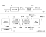
- An example of the system configuration of the communication system 100 is shown schematically.
- An example of the internal configuration of the signal processing unit 170 is shown schematically.
- An example of the system configuration of the phase noise evaluation device 320 is shown schematically.
- An example of the internal configuration of the optical delay interferometer 340 is shown schematically.
- An example of the internal configuration of the optical delay interferometer 540 is shown schematically.
- An example of the internal configuration of the optical delay interferometer 640 is shown schematically.
- An example of the internal configuration of the signal processing unit 370 is shown schematically.
- An example of the system configuration of the phase noise evaluation device 820 is shown schematically.
- An example of the internal configuration of the signal processing section 870 is shown schematically.
- An example of the internal configuration of the optical delay interferometer 1040 is shown schematically.
- An example of the internal configuration of the optical delay interferometer 1140 is shown schematically.
- An example of the internal configuration of the optical delay interferometer 1240 is shown schematically.
- An example of the internal configuration of the optical delay interferometer 1340 is shown schematically.
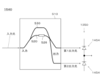
- An example of the circuit configuration of the balanced optical receiver 1350 is shown schematically.
- An example of the internal configuration of the optical delay interferometer 1540 is shown schematically.
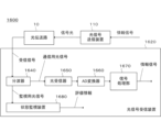
- An example of the system configuration of the communication system 1600 is shown schematically.
- An example of the internal configuration of the optical signal transmitter 110 is shown schematically.
- An example of the internal configuration of the state monitoring device 1680 is shown schematically.
- An example of the internal configuration of the signal processing section 1870 is shown schematically.
- An example of information processing in the state monitoring device 1680 is shown schematically.
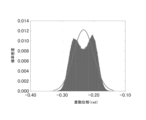
- FIG. 3 shows a differential phase histogram in Experimental Example 1.
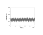
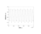
- FIG. 10 shows time variation of the differential phase in Experimental Example 1.
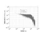
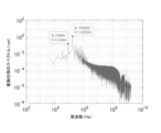
- FIG. 4 shows a frequency spectrum of differential phase in Experimental Example 1.
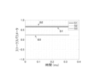
- FIG. 4 shows the measurement results of Stokes parameters in Comparative Experimental Example 1.
- FIG. 3 shows a histogram of differential phases in Comparative Experimental Example 1.
- FIG. 10 shows time variation of the differential phase in Comparative Experimental Example 1.
- FIG. 3 shows a frequency spectrum of a differential phase in Comparative Experimental Example 1.
- FIG. 4 shows the measurement results of Stokes parameters in Experimental Example 2.
- FIG. 10 shows a histogram of differential phases in Experimental Example 2.
- FIG. 10 shows time variation of the differential phase in Experimental Example 2.
- FIG. 10 shows a frequency spectrum of differential phase in Experimental Example 2.
- FIG. 10 shows a frequency spectrum of differential phase in Experimental Example 2.
- phase fluctuations such as optical phase noise and polarization fluctuations can occur in received signals.
- causes of phase fluctuations in received signals include nonlinear optical effects, optical fiber vibrations, optical fiber twists, fluctuations in stress applied to optical fibers, laser linewidth or laser phase fluctuations, and photoelectric effects caused by lightning strikes.
- a field phase change is exemplified.
- a code error may occur in an optical transmission system depending on the phase fluctuation of light.
- an optical transmission system an optical transmission system employing a coherent optical communication scheme is exemplified.
- an apparatus or method for evaluating the presence and/or degree of optical phase noise for example, (i) an apparatus or method for evaluating the presence and/or degree of optical phase noise, (ii) an apparatus or method for evaluating the presence and/or degree of polarization fluctuation and (iii) an example apparatus or method for assessing the presence and/or degree of optical phase noise and polarization variation is described.
- the presence or absence of at least one of optical phase noise and polarization fluctuation and/or the degree of at least one of optical phase noise and polarization fluctuation can be evaluated relatively accurately. As a result, operational efficiency, maintenance efficiency, etc. of the optical transmission system can be improved.
- optical phase noise (sometimes simply referred to as phase noise) has been estimated by linearly approximating the variation of the optical phase with respect to time t.
- the i-th sample point (sometimes referred to as a sample) among N (N is a positive integer) (i is an integer greater than or equal to 1 and less than or equal to N) is approximated using Equation 1 below.
- the phase noise ⁇ (i) can be estimated from the measured value of the phase of the signal light.
- the phase noise ⁇ (i ) cannot be estimated accurately.
- optical phase noise with the 1/f noise component removed can be derived by subtracting the moving average value of the optical phase from the measured phase of the received signal.
- the phase noise ⁇ (i) is derived using Equation 2 below.
- m and l represent integers. The value of l is set appropriately. (Formula 2)
- phase noise is known to be a Wiener process, and phase noise follows a Gaussian distribution whose variance diverges in proportion to time t. Therefore, according to the method described in Non-Patent Document 6, when the time t is short, the variance becomes negative, and the approximate curve cannot be determined accurately due to the influence of the measurement error. there were.
- Nonlinear phase noise includes (i) self-phase modulation phenomenon, (ii) cross-phase modulation phenomenon, and (iii) phenomenon in a fiber Raman amplifier in which intensity noise of pump light generates phase noise in signal light via the Kerr effect. etc. are exemplified.
- Differential phase means the phase difference before and after a sample point (sometimes referred to as a sample).
- the differential phase ⁇ diff (i) at the i-th sample point is expressed as Equation 3 below. (Formula 3)
- the sampling frequency is set equal to or higher than the symbol rate.
- the differential phase can be measured at the same time interval as the symbol time by calculating the differential phase using samples corresponding to appropriate time intervals.
- the time interval between temporally adjacent samples eg, the time interval between the i+1-th sample and the i-th sample
- the sample time interval ⁇ t is sometimes referred to as the sample time interval ⁇ t.
- phase noise ⁇ (t) is obtained using phase ⁇ S (t) of signal light and phase ⁇ L (t) of local oscillation light (sometimes referred to as local light).
- ⁇ (t) ⁇ S (t) ⁇ L (t). Since the phase noise generated in the optical transmission line is included in ⁇ S (t), the above equation shows that ⁇ (t) also includes the phase noise generated in the optical transmission line.
- the phase component at the i-th sample point is calculated by removing the modulated component.
- the modulation component can be canceled by calculating the M-th power of the received signal.
- M is a positive integer.
- the received signal I QPSK (t) represented by a complex number is represented by Equation 5 below.
- IQPSK (t) iI,QPSK (t)+ jiQ,QPSK (t)
- i I,QPSK (t) indicates the output current corresponding to the I signal component obtained by coherent heterodyne detection of the QPSK-modulated optical signal.
- i Q,QPSK (t) indicates an output current corresponding to a Q signal component obtained by coherent heterodyne detection of a QPSK-modulated optical signal.
- QPSK modulation is a quadrature phase shift keying method
- the argument between the received signal I QPSK (t) raised to the 4th power and the phase noise ⁇ (t) is given by Formula 6 below is established.
- f c represents the difference (f s ⁇ f L ) between the angular frequency f s of the signal light and the angular frequency f L of the local light, and is called the beat frequency.
- Equation 8 the differential phase ⁇ diff (i) at the i-th sample point, the phase noise ⁇ (i+1) at the i+1-th sample point, and the phase noise ⁇ (i ) and the sample time interval ⁇ t is represented by the following equation 8. (Formula 8)
- the phase noise ⁇ (i) follows the Gaussian distribution
- the difference, the differential phase ⁇ diff (i) also follows the Gaussian distribution.
- the average value of ⁇ (i) is zero. Therefore, the average value of the differential phase ⁇ diff (i) is 2 ⁇ fc ⁇ t, and if the standard deviation of the phase noise ⁇ (i) of the signal light is ⁇ sig , the variance ⁇ M of the differential phase ⁇ diff (i) is 2 becomes 2 ⁇ sig 2 .
- the phase noise of the signal light can be derived more accurately.
- the measured values are affected by uncertainties due to the length of the moving average time, such as the method of subtracting the moving average value of the optical phase from the measured phase of the received signal. chances are greatly reduced.
- the standard deviation ⁇ sig of the phase noise of the signal light is derived using the standard deviation ⁇ M of the measurement result of the differential phase ⁇ diff (i) of the signal light.
- the standard deviation ⁇ RX of the phase noise of the received signal is derived using Equations 9 to 11.
- the standard deviation ⁇ RX of the phase noise of the received signal is used for purposes such as evaluation and monitoring of transmission effects.
- the differential phase ⁇ diff (i) at each of the N sample points is obtained by converting the light to be measured (sometimes referred to as target light) into an electrical signal, and then the It is derived by signal processing of digital data obtained by sampling and quantizing the electrical signal. For example, time-series data of the phase of the target light is generated at time intervals that are the same as or substantially the same as the symbol time.
- the differential phase ⁇ diff (i) is derived by calculating the difference between two temporally adjacent data in the time-series data.
- the target light is split into the first light and the second light.
- the first light and the second light whose delay time difference ⁇ is adjusted are combined and interfered. After that, the combined light is photoelectrically converted, sampled and quantized to derive the differential phase ⁇ diff (i).
- the differential phase is derived by a relatively simple procedure. Also, the variance or standard deviation of the differential phase is derived by relatively simple arithmetic processing. Therefore, according to this embodiment, the load on the computer can be reduced.
- the modulation component may be mixed into the measurement result and affect the optical phase noise measurement.
- the communication system 100 evaluates phase noise using the optical signal receiving device 120 in, for example, a commissioning test after the communication system 100 is constructed.
- the communication system 100 provides a dedicated wavelength for measuring phase noise during the operation period of the communication system 100, and constantly measures the phase noise of light at the wavelength.
- the phase noise is evaluated by measuring the differential phase of the I and Q components of light at the wavelengths described above.
- the present inventors have found that the above-described differential phase (in particular, the differential phase measured using an optical delay interferometer) includes phase fluctuations caused by polarization fluctuations in addition to optical phase noise. found to be included.
- the amount of transmitted information can be increased by carrying independent data signals in the two orthogonal polarization modes of HE11x and HE11y.
- coupling occurs in both modes during the transmission process of the optical fiber, so high-speed digital signal processing is performed on the receiver side to separate the received signal into the original orthogonal polarization modes.
- phase noise measurement principle In the optical phase noise measurement principle described above, statistical processing is performed in the process of deriving the phase noise of signal light. Therefore, sudden phase fluctuations are less likely to be reflected in the measurement results of the phase noise of the signal light. Therefore, by detecting the phase fluctuation caused by the sudden polarization fluctuation based on the measurement result in real time, not only by grasping the statistic such as the standard deviation, the optical transmission system and/or the optical signal The condition can be assessed more accurately.
- E x (t) and E y (t) be the orthogonal polarization modes of the signal light propagating in the z direction, and k x and ky be the unit vectors in the x and y directions.
- the electric field of the light received by the receiver (sometimes referred to as the received optical electric field) E(t) is expressed by the following equation B-1.
- E(t) [E x (t)cos ⁇ 2 ⁇ ft+ ⁇ n (t) ⁇ k x +E y (t) cos ⁇ 2 ⁇ ft+ ⁇ n (t)+ ⁇ (t) ⁇ k y ]
- ⁇ (t) represents the phase difference between E x (t) and E y (t).
- ⁇ n (t) represents optical phase noise.
- f represents the frequency of signal light.
- E(t), k x and k y are vectors.
- Equation B-2 R ⁇ E(t)+E(t- ⁇ ) ⁇ E(t)+E(t- ⁇ ) ⁇
- Equation B-2 ⁇ represents the delay time difference between the two paths of the optical delay interferometer.
- R represents the sensitivity of the optical receiver.
- ⁇ indicates the inner product.
- Equation B-3 Equation B-3
- the received current i is represented by the following equation B-5. (Formula B-5)
- Equation B-6 the above received current i is caused by the polarization fluctuation represented by Equation B-7 below, in addition to the term caused by the phase noise of the signal light propagating through the optical transmission line.
- the received current i obtained by adding the fluctuation due to the polarization fluctuation is observed.
- phase fluctuations caused by sudden polarization fluctuations can be detected based on the real-time measurement results of the received current i.
- Equation B-8 the amplifier output current i pol_LPF is given by equation B-9 below.
- An amplifier may be an example of an integrator circuit.
- Equation B-9 holds within the range where the above low-pass filter operates as an integrating circuit. That is, Equation B-9 holds for frequencies equal to or higher than the cutoff frequency of the low-pass filter.
- Equation B-9 holds for frequencies equal to or higher than the cutoff frequency of the low-pass filter.
- Equation B-6 since the term resulting from phase noise in Equation B-6 is a stochastic process, the term resulting from phase noise is not phase continuous. Therefore, integration effects in the amplifier do not act on terms due to phase noise. As a result, the term due to phase noise in Equation B-6 is output from the amplifier as Equation B-6.
- phase noise component a term due to phase noise
- polarization fluctuation sometimes referred to as a polarization fluctuation component
- the phase noise component is preferably measured during a period when the polarization fluctuation component is small. Therefore, for example, when the occurrence of polarization fluctuation is detected, an alarm is output, the measurement data of the received current i is given a flag indicating that the polarization fluctuation is detected, or the polarization fluctuation is detected.
- the measurement and/or analysis of phase noise can be effectively carried out by recording the time taken.
- Equation B-12 described above does not necessarily hold.
- Equation B-7 holds. Therefore, when the output current i of the optical receiver connected to the optical delay interferometer is amplified by, for example, an amplifier following the optical receiver, ⁇ (t) is integrated under the constraint of a sine function.
- ⁇ (t) fluctuates between - ⁇ /2 ⁇ ⁇ (t) ⁇ ⁇ /2.
- the value of sin ⁇ (t)- ⁇ (t- ⁇ ) ⁇ is at most -1 ⁇ sin ⁇ (t)- ⁇ (t- ⁇ ) ⁇ 1.
- the spectrum component obtained by Fourier transforming the measurement result of i pol represented by Equation B-7 becomes the amplitude value of the fluctuation.
- Equations B-13, B-14, B-15 and B-16 indicate ellipticity. ⁇ indicates the orientation of the elliptically polarized light. Equations B-13, B-14, B-15 and B-16 show the relationship between rectangular coordinates (S 1 , S 2 , S 3 ) and polar coordinates (S 0 , 2 ⁇ , 2 ⁇ ).
- a sphere of radius S 0 in Cartesian coordinates (S 1 , S 2 , S 3 ) is called a Poincare sphere, the longitude of which represents twice the orientation ⁇ , and the latitude of the Poincare sphere represents twice the ellipticity ⁇ . show.
- the UOQ formed by the Cartesian origin O(0,0,0), the point U(S 1 ,S 2 ,0) on the Poincare sphere, and the point Q(S 1 ,0,0) on the Poincare sphere is 2 ⁇ .
- Equation B-8 As described above, by measuring the output current i of the optical receiver connected to the optical delay interferometer, the phase variation approximated by Equation B-8 is observed. Assuming that d ⁇ DL is the result of converting the above phase variation amount into d ⁇ described above, d ⁇ DL is expressed by the following equation B-18 using the power ratio ⁇ described above. (Formula B-18)
- the measured phase variation on the Poincare sphere is c(t) times the moving angle on the Poincare sphere.
- c(t) is represented by B-19 below.
- Equation B-20 The relationship between c(t) and ⁇ described above is represented by Equation B-20 below.
- ⁇ may be greater than 0 and less than 1.
- ⁇ When ⁇ is 0 or 1, the electric field is concentrated on HE11x or HE11y, resulting in perfect linear polarization. Therefore, when ⁇ is 0 or 1, there is no need to consider the concept of polarization variation.
- the phase fluctuation amplitude width measured by the optical delay interferometer represents an approximate value of the moving angle (that is, the phase change amount) of the trajectory on the Poincare sphere.
- the above phase fluctuation amplitude width is obtained as the amplitude value of the frequency component giving the peak in the Fourier transform result of the output current of the optical receiver.
- FIG. 1 schematically shows an example of a system configuration of a communication system 100. As shown in FIG. In this embodiment, the signal light output from the optical signal transmitting device 110 propagates through the optical transmission line 10 and reaches the optical signal receiving device 120, thereby transmitting an information signal. 100 details are described.
- the optical transmission line 10 transmits light.
- An optical fiber is exemplified as the optical transmission line 10 .
- the communication system 100 includes an optical signal transmitter 110 and an optical signal receiver 120 .
- the optical signal receiving device 120 includes a local oscillator 130, an optical 90-degree hybrid 140, an optical receiver 152, an optical receiver 154, an AD converter 162, an AD converter 164, a signal processing and a section 170 .
- the optical signal transmission device 110 generates an optical signal.
- Optical signal transmitter 110 generates a polarization multiplexed optical signal, for example, by modulating an optical carrier with an information signal to be transmitted.
- the optical signal may be a signal on which a symbol time series is superimposed.
- the optical signal transmitter 110 outputs light (sometimes referred to as signal light) forming an optical signal.
- the signal light is transmitted to the optical signal receiver 120 via the optical transmission line 10 .
- the optical signal receiving device 120 receives signal light propagated through the optical transmission line 10 .
- the optical signal receiver 120 demodulates the received optical signal to generate an information signal.
- the optical signal receiving device 120 derives an index for evaluating the phase noise of signal light. Thereby, the optical signal receiving device 120 can evaluate the phase noise of the signal light propagated through the optical transmission line 10 .
- the above index may be an index that indicates the degree of phase noise of the signal light.
- the degree of variation in differential phase of signal light is employed as the index.
- dispersion or standard deviation is exemplified.
- the local oscillator 130 outputs local oscillation light (sometimes referred to as local light, as described above). Local light emitted from the local oscillator 130 is input to the optical 90-degree hybrid 140 .
- the optical 90-degree hybrid 140 causes the signal light propagated through the optical transmission line 10 to interfere with the local light emitted from the local oscillator 130, so that the received signal transmitted by the signal light is divided into a plurality of signal components. It outputs a plurality of separated optical signals.
- the optical 90-degree hybrid 140 mixes the signal light and the local light and outputs two optical signals that are 90 degrees out of phase. The above two signals are sometimes referred to as the I and Q signals, respectively.
- the optical receiver 152 converts an optical signal into an electrical signal.
- the optical receiver 152 converts the I signal of the received signal transmitted by the signal light into an electrical signal. This converts the I signal from an optical signal to an electrical signal.
- the optical receiver 152 outputs an electrical signal corresponding to the I signal to the AD converter 162 .
- the optical receiver 154 converts optical signals into electrical signals.
- the optical receiver 154 converts the Q signal of the received signal transmitted by signal light into an electrical signal. This converts the Q signal from an optical signal to an electrical signal.
- Optical receiver 154 outputs an electrical signal corresponding to the Q signal to AD converter 164 .
- the AD converter 162 converts the electrical signal from an analog signal to a digital signal.
- the AD converter 162 converts the electrical signal corresponding to the I signal into a digital signal.
- the AD converter 162 converts a plurality of digital signals (sampled I signal ) is output to the signal processing unit 170 .
- the time intervals between the multiple time points may be substantially constant.
- the sampling rate of the AD converter 162 may be equal to or higher than the symbol rate of the received signal. This sets the sample time interval to be less than or equal to the length of the symbol time.
- the sampling rate of AD converter 162 may be the same as the symbol rate of the received signal. This sets the sample time interval to the length of the symbol time.
- the AD converter 164 converts the electrical signal from an analog signal to a digital signal.
- the AD converter 164 converts the electrical signal corresponding to the Q signal into a digital signal.
- the AD converter 164 outputs a plurality of digital signals (sometimes referred to as sampled Q signals) respectively corresponding to a plurality of points in time during the evaluation period to the signal processing section 170 .
- the time intervals between the multiple time points may be substantially constant.
- the sampling rate of the AD converter 164 may be equal to or higher than the symbol rate of the received signal. This sets the sample time interval to be less than or equal to the length of the symbol time.
- the sampling rate of AD converter 164 may be the same as the symbol rate of the received signal. This sets the sample time interval to the length of the symbol time.
- the signal processing unit 170 demodulates the received signal transmitted by signal light and generates an information signal. Also, in this embodiment, the signal processing unit 170 evaluates the phase noise of the signal light propagated through the optical transmission line 10 . The signal processor 170 may monitor the phase noise of the signal light propagated through the optical transmission line 10 . Details of the signal processing unit 170 will be described later.
- Each unit of the communication system 100 may be realized by hardware, software, or both hardware and software. At least part of each part of the communication system 100 may be realized by an analog circuit or by a digital circuit. At least part of each part of the communication system 100 may be realized by a single server or may be realized by a plurality of servers. At least part of each unit of the communication system 100 may be realized on a virtual machine or a cloud system. At least part of each unit of the communication system 100 may be realized by a personal computer or a mobile terminal. Examples of mobile terminals include mobile phones, smart phones, PDAs, tablets, notebook or laptop computers, wearable computers, and the like. Each part of communication system 100 may utilize distributed ledger technology or distributed networks, such as blockchain, to store information.
- distributed ledger technology or distributed networks, such as blockchain to store information.
- the components implemented by the software define operations related to the components in an information processing apparatus with a general configuration. It may be realized by starting a program.
- the above information processing device includes, for example, (i) a data processing device having a processor such as a CPU and GPU, a ROM, a RAM, a communication interface, and the like; and (ii) a keyboard, touch panel, camera, microphone, various sensors, and a GPS receiver. (iii) an output device such as a display device, a speaker, and a vibration device; and (iv) a storage device (including an external storage device) such as a memory and an HDD.
- a data processing device having a processor such as a CPU and GPU, a ROM, a RAM, a communication interface, and the like; and (ii) a keyboard, touch panel, camera, microphone, various sensors, and a GPS receiver.
- an output device such as a display device, a speaker, and a vibration device
- a storage device including an external storage device
- the above data processing device or storage device may store a program.
- the above program may be stored in a non-transitory computer-readable recording medium.
- the program is executed by the processor to cause the information processing apparatus to perform operations specified by the program.
- the program may be stored in a computer-readable medium such as a CD-ROM, DVD-ROM, memory, hard disk, etc., or may be stored in a storage device connected to a network.
- the program may be installed on a computer forming at least part of communication system 100 from a computer-readable medium or network-attached storage device. By executing the program, the computer may function as at least part of each unit of the communication system 100 .
- a program that causes a computer to function as at least part of each unit of the communication system 100 may include modules that define the operation of each unit of the communication system 100 . These programs or modules work on the data processing device, input device, output device, storage device, etc., to make the computer function as each part of the communication system 100, or to make the computer execute the information processing method in each part of the communication system 100. or
- the information processing described in the program functions as concrete means in which the software related to the program and various hardware resources of the communication system 100 cooperate with each other when the program is read into the computer. Then, the communication system 100 is constructed according to the purpose of use of the computer according to the present embodiment by realizing the calculation or processing of information according to the purpose of use of the computer by the specific means described above.
- the above program may be a program for causing a computer to function as the optical signal receiving device 120 or a part thereof.
- the above program may be a program for causing a computer to execute an information processing method in the optical signal receiving device 120 or part thereof.
- an AD converter 162 As a part of the optical signal receiving device 120, an AD converter 162, an AD converter 164, a signal processing section 170, etc. are exemplified.
- the information processing method may be an evaluation method for evaluating phase noise of signal light propagated through an optical transmission line.
- the evaluation method described above has, for example, a differential phase information obtaining step of obtaining information indicating the differential phase of the input light at each of a plurality of points in time included in the evaluation period.
- the above evaluation method has an index derivation step of deriving the degree of differential phase variation at each of a plurality of time points as an index for evaluating phase noise.
- the differential phase represents, for example, the phase difference of the input light at two temporally adjacent points of time among a plurality of points of time.
- the time intervals between the multiple time points are, for example, substantially constant.
- the time interval between the points in time is, for example, equal to or less than the length of the symbol time of the signal transmitted by the input light.
- the communication system 100 may be an example of an optical communication system.
- Optical signal transmitter 110 may be an example of an optical transmitter.
- Optical signal receiver 120 may be an example of an evaluation device or optical receiver.
- Local oscillator 130 may be an example of a local light source.
- the optical receiver 152 may be an example of a photoelectric converter.
- the optical receiver 154 may be an example of a photoelectric converter.
- the AD converter 162 may be an example of an analog-to-digital converter.
- AD converter 164 may be an example of an analog-to-digital converter.
- the signal processor 170 may be an example of an evaluation device.
- the I signal may be an example of an optical signal of I signal components.
- the sampled I signal may be an example of the first digital signal.
- the Q signal may be an example of a Q signal component optical signal.
- the sampled Q signal may be an example of the second digital signal.
- the target light may be an example of input light. Light that constitutes various optical signals may be
- FIG. 2 schematically shows an example of the internal configuration of the signal processing section 170.
- the signal processing section 170 includes a digital signal processing circuit 210 , a decoding circuit 220 , an amplitude noise evaluation section 230 and a phase noise evaluation section 240 .
- the phase noise estimator 240 comprises a differential phase signal generator 242 , a histogram generator 244 and a standard deviation calculator 246 .
- the digital signal processing circuit 210 receives the sampled I signal from the AD converter 162 .
- Digital signal processing circuit 210 receives the sampled Q signal from AD converter 164 .
- the digital signal processing circuit 210 uses the I and Q signals to perform various digital signal processing for demodulating and compensating the received signal.
- the decoding circuit 220 executes error correction processing, decoding processing, and the like. Thereby, the information signal is extracted from the received signal.
- the amplitude noise evaluation section 230 evaluates the amplitude noise of the signal light propagated through the optical transmission line 10 .
- the amplitude noise evaluation unit 230 derives various indices for evaluating the amplitude noise of the signal light propagated through the optical transmission line 10 .
- An optical signal-to-noise ratio or the like is exemplified as the index.
- the optical signal-to-noise ratio is measured using a sampled I signal and/or a sampled Q signal. For example, when the optical signal-to-noise ratio of signal light is measured using a sampled I signal, the I signal is input to amplitude noise evaluation section 230 .
- the amplitude noise evaluation section 230 includes an average value calculation section, a histogram generation section, and a standard deviation calculation section. Thereby, the amplitude noise of the signal light is measured.
- the phase noise evaluation unit 240 evaluates the phase noise of the signal light propagated through the optical transmission line 10.
- the phase noise evaluation unit 240 derives various indices for evaluating the phase noise of the signal light propagated through the optical transmission line 10 .
- the degree of variation in the differential phase is exemplified as the index. Examples of indices indicating the degree of variation include variance and standard deviation.
- the phase noise evaluation unit 240 derives the standard deviation of the differential phase during the evaluation period as an index indicating the degree of variation in the measured differential phase.
- An example of part 240 is described.
- the phase noise estimator 240 is not limited to this embodiment. It should be noted that in another embodiment, the phase noise estimator 240 may derive the variance of the differential phase during the evaluation period as an indicator of the degree of differential phase variation.
- the differential phase signal generator 242 receives, for example, the data of the I signal and the data of the Q signal at each of N (N is a positive integer) sample points during the evaluation period from the digital signal processing circuit 210 .
- N is a positive integer
- Each of the N sample points corresponds to each of multiple time points included in the evaluation period.
- the differential phase signal generator 242 determines the phase of the signal light measured at each of the N sample points based on the I signal data and the Q signal data at each of the N sample points.
- the phase of the signal light at the i-th sample point (where i is an integer of 1 or more and (N ⁇ 1) or less) is determined according to Equation 4 described above, for example.
- the differential phase signal generator 242 calculates the value of the differential phase at each of the N sample points based on the measured value of the phase of the signal light at each of the N sample points.
- the differential phase value ⁇ diff (i) at the i-th sample point is calculated, for example, according to Equation 3 described above.
- Equation 3 the difference in the phase of the signal light at two temporally adjacent time points among the plurality of time points is calculated.
- the differential phase signal generator 242 can acquire information indicating the differential phase of the signal light at each of a plurality of points in time included in the evaluation period.
- the differential phase signal generator 242 may remove the modulation component and generate information indicating the differential phase at each of the N sample points.
- the differential phase signal generator 242 removes the modulation component contained in the received signal, for example, based on the multiple sampled I and Q signals. As described above, in the case of M-phase modulation, the modulation component can be canceled by calculating the M-th power of the received signal.
- the histogram generator 244 acquires information indicating (N-1) differential phases (sometimes referred to as differential phase signals) from the differential phase signal generator 242. .
- the histogram generator 244 generates histograms of (N ⁇ 1) differential phases.
- the histogram generator 244 outputs information indicating the generated histogram to the standard deviation calculator 246 .
- the standard deviation calculator 246 calculates the standard deviation of (N-1) differential phases. For example, the standard deviation calculator 246 fits the histogram generated by the histogram generator 244 to a normal distribution. Also, the standard deviation calculator 246 calculates the standard deviation of the above normal distribution.
- the standard deviation calculator 246 may derive the calculated standard deviation as an index for evaluating the phase noise of the signal light. As shown in Equation 6, the square of the standard deviation of the phase noise of the signal light is expressed as 1/2 times the square of the standard deviation of the differential phase. The standard deviation calculator 246 may derive the standard deviation of the phase noise of the signal light according to Equation 9 based on the standard deviations of the (N ⁇ 1) differential phases.
- the square of the standard deviation of the phase noise of the received signal is the sum of the square of the standard deviation of the phase noise of the signal light and the standard deviation of the phase noise due to the spectral line width of the local oscillation light. It is expressed as the square root of the sum of the powers.
- the standard deviation calculator 246 may derive the standard deviation of the phase noise of the received signal according to Equations 9 to 11 based on the standard deviations of the N differential phases.
- the standard deviation calculator 246 may generate information for evaluating phase noise of signal light (sometimes referred to as evaluation information). Examples of the information for evaluating the phase noise of the signal light include information indicating the standard deviation of the N differential phases, the standard deviation of the phase noise of the signal light, and/or the standard deviation of the phase noise of the received signal. be done.
- the phase noise evaluation unit 240 may be an example of an evaluation device.
- the differential phase signal generation section 242 may be an example of a differential phase information acquisition section.
- the histogram generation section 244 may be an example of a differential phase information acquisition section.
- the standard deviation calculator 246 may be an example of an index derivation unit.
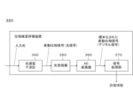
- FIG. 3 schematically shows an example of the system configuration of the phase noise evaluation device 320.
- the phase noise evaluation device 320 includes an optical delay interferometer 340 , an optical receiver 350 , an AD converter 360 and a signal processor 370 .
- the optical signal receiver 120 performs high-speed A/D conversion and digital signal processing to determine the standard deviation of the differential phase at the evaluation facility. was calculated.
- the present embodiment differs from the optical signal receiving apparatus 120 described with reference to FIGS. 1 and 2 in that high-speed arithmetic processing on electrical signals in the optical signal receiving apparatus 120 is performed at the optical level.
- the phase noise evaluation device 320 measures the degree of variation in the differential phase of the light input to the phase noise evaluation device 320 (sometimes referred to as input light). Output as an index for evaluation. Thereby, the phase noise evaluation device 320 can evaluate the phase noise of the input light.
- the above input light may be signal light propagated through the optical transmission line 10 or output light from the optical 90-degree hybrid 140 .
- the phase noise evaluation device 320 is attached to the optical signal receiving device 120, for example, and receives a portion of the signal light propagated through the optical transmission line 10 as input.
- the optical signal In the signal light used for actual communication, the optical signal has spectral components due to modulation. Therefore, the modulation component is mixed in the measurement result, and it may become difficult to measure the optical phase noise.
- the phase noise estimator 320 is attached to the communication system 100, for example, to evaluate the phase noise in a commissioning test after the communication system 100 is built.
- the phase noise evaluation device 320 provides a dedicated wavelength for measuring phase noise during the operation period of the communication system 100, and constantly measures the phase noise of light at that wavelength. Attached to communication system 100 .
- the phase noise is evaluated by measuring the differential phase of the I and Q components of light at the wavelengths described above.
- the optical delay interferometer 340 receives light (sometimes referred to as input light, target light, etc.).
- the optical delay interferometer 340 has, for example, a first optical path and a second optical path.
- the optical delay interferometer 340 for example, splits input light into first input light and second input light.
- the optical delay interferometer 340 causes, for example, the first input light that has passed through the first optical path and the second input light that has passed through the second optical path to interfere with each other.
- the first optical path and the second optical path of the optical delay interferometer 340 have a delay time difference ⁇ between the first input light that has passed through the first optical path and the second input light that has passed through the second optical path, and and the frequency f are set so as to satisfy the relationship of Equation 12 below.
- Equation 13 the output current i of the optical receiver 350 to which the output light of the optical delay interferometer 340 is input is approximated by Equation 13 below.
- i RE 2 ⁇ n(t) ⁇ n(t ⁇ ) ⁇ 12 above
- R is the sensitivity of the optical receiver 350 .
- E is the electric field of the first input light and the second input light.
- ⁇ n(t) is the phase noise of the input light at time t.
- the optical receiver 350 converts the output light of the optical delay interferometer 340 into an electrical signal.
- the output current of optical receiver 350 indicates the differential phase of the input light at each of the multiple times included in the evaluation period.
- the optical receiver 350 can obtain information indicating the differential phase of the input light at each of the plurality of points in time included in the evaluation period.
- the differential phase represents the phase difference of input light at two temporally adjacent points of time among a plurality of points of time.
- the AD converter 360 converts the electrical signal output by the optical receiver 350 from an analog signal to a digital signal.
- the AD converter 360 outputs to the signal processing section 370 a plurality of digital signals corresponding to the differential phases at each of the plurality of points in time included in the evaluation period.
- the time intervals between the multiple time points may be substantially constant.
- the sampling rate of the AD converter 360 can be significantly reduced compared to the sampling rate of the AD converter 162 or the AD converter 164 that samples the signal light. For example, if the sample rate of communication light is 100 GS/s, the sample rate of AD converter 360 can be reduced to approximately 1 GS/s.
- the optical delay interferometer 340 when the optical delay interferometer 340 is used, a value obtained by converting the differential phase into intensity is measured. That is, the optical delay interferometer 340 converts the differential phase noise into amplitude noise. Also, the frequency components of the differential phase noise are almost white noise.
- a narrow-band optical receiver can be used as the optical receiver 350 . Specifically, an optical receiver having a band of approximately 100 MHz is used as the optical receiver 350 . Thereby, the sampling rate of the AD converter 360 that samples the output current of the optical receiver 350 can also be reduced.
- the signal processing unit 370 receives the multiple digital signals described above from the AD converter 360 .
- the signal processing unit 370 derives the degree of variation in the differential phase at each of the plurality of points of time as an index for evaluating the phase noise of the input light.
- standard deviation, dispersion, and the like are examples of indices that indicate the degree of variation.
- the square of the standard deviation of the phase noise of the input light is expressed as 1/2 times the square of the standard deviation of the differential phase.
- the signal processing section 370 may output information indicating the evaluation of the phase noise of the input light (sometimes referred to as evaluation information). Details of the signal processing unit 370 will be described later.
- high-speed arithmetic processing for electrical signals in the optical signal receiving device 120 is performed at the optical level.
- power saving and cost reduction can be achieved.
- the reciprocal of the delay time is equivalent to the sampling rate in the AD converter. As such, the power used for sampling can be saved.
- the phase noise evaluation device 320 may be an example of an evaluation device.
- the optical delay interferometer 340 may be an example of a delay interferometer.
- the optical receiver 350 may be an example of a differential phase information acquisition section or a photoelectric conversion section.
- AD converter 360 may be an example of a differential phase information acquisition unit or an analog-to-digital conversion unit.
- the signal processor 370 may be an example of a differential phase information acquisition unit or an index derivation unit.
- phase noise evaluation device 320 In the present embodiment, an example of the phase noise evaluation device 320 has been described using the case where the phase noise evaluation device 320 includes the AD converter 360 and the signal processing section 370 as an example. However, the phase noise evaluation device 320 is not limited to this embodiment. In another embodiment, the signal processing section 370 may have the function of the AD converter 360 and the phase noise evaluation device 320 may not include the AD converter 360 .
- the optical delay interferometer 340 includes a semi-transmissive mirror 422 , a semi-transmissive mirror 424 , a total reflection mirror 432 , a total reflection mirror 434 and an optical phase adjuster 436 .
- the input light is split into first signal light that passes through the semi-transmissive mirror 422 and second signal light that is reflected by the semi-transmissive mirror 422 .
- the first signal light is transmitted through the semitransparent mirror 424 and output from the optical delay interferometer 340 .
- the second signal light is reflected by the total reflection mirror 432 , the total reflection mirror 434 and the semi-transmissive mirror 424 , mixed with the first signal light transmitted through the semi-transmissive mirror 424 , and emitted from the optical delay interferometer 340 . output.
- the optical delay interferometer 340 gives an optical path difference to the first signal light and the second signal light.
- ⁇ be the delay time difference due to the above optical path difference
- t be the time
- ⁇ (t) be the phase of the input of the first signal light to the optical receiver 350 .
- the phase at the time of input is ⁇ (t ⁇ ).
- the delay time difference ⁇ is adjusted to satisfy the relationship of Equation 8 described above.
- optical phase adjuster 436 adjusts the phase of light passing through optical phase adjuster 436 .
- optical phase adjuster 436 adjusts the phase of light passing through optical phase adjuster 436 in response to the voltage applied to optical phase adjuster 436 .
- the optical phase adjuster 436 include a liquid phase element and a lithium niobate crystal.
- the delay time difference ⁇ is adjusted by adjusting the distance between the first optical path and the second optical path and/or the voltage applied to the optical phase adjuster 436 . This allows the operating point of the optical delay interferometer 340 to be adjusted.
- the delay time difference ⁇ may be adjusted during calibration or may be adjusted in real time.
- the optical phase adjuster 436 may be arranged in a region of the first optical path that does not overlap with the second optical path. Also, the optical delay interferometer 340 may not have the optical phase adjuster 436 .
- FIG. 5 schematically shows an example of the internal configuration of the optical delay interferometer 540.
- FIG. Optical delay interferometer 540 is another example of optical delay interferometer 340 and may be implemented in phase noise evaluation apparatus 320 instead of optical delay interferometer 340 .
- the optical delay interferometer 540 includes a substrate 510 and waveguides 520 and 530 formed on the substrate 510 .
- Substrate 510 may be a semiconductor substrate, such as a silicon substrate.
- the input light splits into the waveguide 520 and the waveguide 530 at the split point. After the first signal light propagating through the waveguide 520 and the second signal light propagating through the waveguide 530 are combined, they are output from the optical delay interferometer 540 .
- the delay time difference ⁇ of waveguides 520 and 530 is adjusted to satisfy the relationship of Equation 8 described above.
- an electrode 526 is arranged in part of the waveguide 520 .
- the phase of light passing through waveguide 520 is finely adjusted.
- the delay time difference ⁇ is adjusted by adjusting the distance between the waveguides 520 and 530 and/or the voltage applied to the electrode 526 . This allows the operating point of the optical delay interferometer 540 to be adjusted.
- the delay time difference ⁇ may be adjusted during calibration or may be adjusted in real time.
- the electrode 526 may be arranged in the waveguide 530 in another embodiment. Also, the optical delay interferometer 540 may not have the electrode 526 .
- the optical delay interferometer 640 includes a substrate 610, a waveguide 620 into which input light is input, a ring resonator 630 arranged adjacent to the waveguide 620, and a portion of the ring resonator 630. and an electrode 636 arranged in the .
- Substrate 610 may be a semiconductor substrate, such as a silicon substrate.
- the input light incident from the input terminal propagates through the waveguide 620 and reaches the ring resonator 630 .
- a portion of the input light is then introduced into ring resonator 630 .
- the input/output characteristics of the ring resonator 630 are set such that the length of the ring is an integer multiple of the wavelength of the input light in the ring medium.
- the output current specification with respect to the optical frequency becomes steeper in the vicinity of the operating point.
- Light passing through waveguide 620 is output from optical delay interferometer 640 and input to optical receiver 350 .
- the optical phase in ring resonator 630 is adjusted by the voltage applied to electrode 636 . This allows the operating point of the optical delay interferometer 640 to be adjusted.
- FIG. 7 schematically shows an example of the internal configuration of the signal processing section 370.
- the signal processor 370 includes a histogram generator 244 , a standard deviation calculator 246 and a calibrator 710 .
- the calibration unit 710 executes various calibration processes. As described above, the output current i of optical receiver 350 is approximated by Equation 13. Therefore, the calibration unit 710 performs calibration processing of the phase noise evaluation device 320 using signal light with known phase noise. Thereby, the reception sensitivity of the optical receiver 350 and the noise of the electric circuit of the optical receiver 350 are calibrated.
- the variance of the differential phase noise is derived by subtracting the variance of the electrical circuit noise from the variance of the received signal. Also measured by the above derivation is the intensity noise corresponding to the statistical distribution of the phase noise. Therefore, measurement results such as the above-mentioned various dispersions and standard deviations derived from the dispersions can be calibrated in advance with reference to known optical phase noise. The same is true when an optical ring resonator is used.
- FIG. 8 schematically shows an example of the system configuration of the phase noise evaluation device 820.
- the phase noise evaluation device 820 differs from the phase noise evaluation device 320 in that it includes an optical receiver 850 , an AD converter 860 and an optical phase controller 880 .
- the input light is split at the branch point into the first light incident on the optical delay interferometer 340 and the second light incident on the optical receiver 850 .
- the phase noise evaluation device 820 differs from the phase noise evaluation device 320 in that it includes a signal processing section 870 instead of the signal processing section 370 .
- the phase noise evaluation device 820 may have the same configuration as the phase noise evaluation device 320 with respect to features other than the differences described above.
- the optical receiver 850 converts the input second light into an electrical signal.
- the AD converter 860 converts the electrical signal output by the optical receiver 850 from an analog signal to a digital signal. This provides information indicating the measured value of the optical power of the input light.
- the signal processing unit 870 acquires information indicating the measured optical power of the input light from the AD converter 860 .
- the signal processor 870 normalizes the differential phase of the input light using the measured optical power of the input light. Also, the signal processing section 870 derives the degree of dispersion of the differential phase using the normalized differential phase.
- the optical phase controller 880 acquires an electrical signal corresponding to the output light of the optical delay interferometer 340 from the optical receiver 350 .
- the optical phase controller 880 adjusts the operating point of the optical delay interferometer 340 based on the electrical signal.
- the optical phase controller 880 controls the optical delay interferometer 340 so that the operating point of the optical delay interferometer 340 is the point at which the ratio of the output current variation to the optical frequency variation is greater than a predetermined value. Adjust the operating point of 340.
- the optical phase control unit 880 adjusts the operating point of the optical delay interferometer 340 so that the ratio of the output current variation to the optical frequency variation is substantially maximum. may be adjusted.
- the optical frequency versus output current characteristic of the optical delay interferometer 340 is sinusoidal with respect to the optical frequency, and its period is 1/ ⁇ . Therefore, in the graph of the optical frequency vs. output current characteristic, if the point where the sine wave crosses 0 is set as the operating point, the ratio of the amount of variation in the output current to the amount of variation in the optical frequency is approximately maximum. I know it will be.
- the optical phase control section 880 may determine the position where the average value of the output current is 0 as the operating point of the optical delay interferometer 340 .
- the optical frequency in the optical frequency vs. output current characteristic (that is, the vertical axis is the output current and the horizontal axis is the optical frequency graph) can be considered in terms of the differential phase.
- the fluctuation of the phase becomes the fluctuation of the output current as it is.
- the AD converter 860 may be an example of an optical power information acquisition unit.
- the signal processor 870 may be an example of an optical power information acquisition unit.
- the optical phase control section 880 may be an example of an adjustment section.
- the optical phase control unit 880 detects the average value of the output current of the optical receiver 350, and sets the operating point of the optical delay interferometer 340 so that the average value becomes 0. , an example of the optical phase control unit 880 has been described. However, the optical phase controller 880 is not limited to this embodiment.
- the optical phase controller 880 may detect the peak-to-peak value of the output current of the optical receiver 350 and set the operating point of the optical delay interferometer 340 so that the value is maximized. Similarly, the optical phase controller 880 may detect the value of the amplitude of the output current of the optical receiver 350 and set the operating point of the optical delay interferometer 340 so that the value is maximized.
- FIG. 9 schematically shows an example of the internal configuration of the signal processing section 870.
- the signal processor 870 includes a histogram generator 244 , a standard deviation calculator 246 , a calibrator 710 and a normalizer 930 .
- the normalization unit 930 acquires information indicating the measured optical power of the input light from the AD converter 860 .
- the normalization unit 930 normalizes the differential phase of the input light using the measured optical power of the input light.
- the normalization section 930 outputs information indicating the normalized differential phase of the input light to the histogram generation section 244 .
- the histogram generator 244 uses the normalized differential phase to generate a differential phase histogram.
- the standard deviation calculator 246 derives the standard deviation of the differential phase using a histogram generated by returning to the normalized differential phase.
- FIG. 10 schematically shows an example of the internal configuration of the optical delay interferometer 1040.
- the optical delay interferometer 340 is provided with a semitransmissive mirror 1060 for splitting the input light and inputting a part of the input light to the optical receiver 850 .
- the optical delay interferometer 1040 differs from the optical delay interferometer 340 in that the voltage applied to the optical phase adjuster 436 is controlled by the optical phase controller 880 .
- FIG. 11 schematically shows an example of the internal configuration of the optical delay interferometer 1140.
- the optical delay interferometer 1140 is similar to the optical delay interferometer 540 in that a waveguide 1160 is provided for branching the input light and inputting part of the input light to the optical receiver 850 . differ. Further, in this embodiment, the optical delay interferometer 1140 differs from the optical delay interferometer 540 in that the voltage applied to the electrode 526 is controlled by the optical phase controller 880 .
- the optical delay interferometer 1240 schematically shows an example of the internal configuration of the optical delay interferometer 1240.
- the optical delay interferometer 1240 is similar to the optical delay interferometer 640 in that a waveguide 1260 is provided for branching the input light and inputting a part of the input light to the optical receiver 850. differ. Further, in this embodiment, the optical delay interferometer 1240 differs from the optical delay interferometer 640 in that the voltage applied to the electrode 636 is controlled by the optical phase controller 880 .
- FIG. 13 schematically shows an example of the internal configuration of the optical delay interferometer 1340.
- the optical delay interferometer 1340 differs from the optical delay interferometer 340 in that a balanced optical receiver 1350 is used instead of the optical receiver 350 . Thereby, the intensity noise contained in the signal light can be suppressed.
- the balanced optical receiver 1350 includes an optical receiver 1352 , an optical receiver 1354 and a differential processing section 1356 .
- the optical receiver 1352 receives the first output light obtained by combining the first signal light transmitted through the semi-transmissive mirror 424 and the second signal light reflected by the semi-transmissive mirror 424 .
- a second output light obtained by combining the first signal light reflected by the semi-transmissive mirror 424 and the second signal light transmitted through the semi-transmissive mirror 424 is input to the optical receiver 1354 .
- the differential processor 1356 outputs an electrical signal corresponding to the difference between the output of the optical receiver 1352 and the output of the optical receiver 1354 to the AD converter 360 .
- the balanced optical receiver 1350 comprises a photodiode 1452 and a photodiode 1454 connected in series.
- Balanced optical receiver 1350 outputs an electrical signal from junction 1456 of photodiode 1452 and photodiode 1454 .
- the optical delay interferometer 15 schematically shows an example of the internal configuration of the optical delay interferometer 1540.
- the optical delay interferometer 1540 differs from the optical delay interferometer 540 in that a balanced optical receiver 1350 is used instead of the optical receiver 350 . Thereby, the intensity noise contained in the signal light can be suppressed.
- FIG. 16 schematically shows an example system configuration of a communication system 1600. As shown in FIG. In this embodiment, the signal light output from the optical signal transmitting device 110 propagates through the optical transmission line 10 and reaches the optical signal receiving device 1620, thereby transmitting an information signal. 100 details are described.
- the communication system 1600 may have the same configuration as the communication system 100, except that the communication system 1600 has a configuration for detecting polarization variations. Regarding the details of the communication system 1600, descriptions of configurations similar to those of the communication system 100 may be omitted.
- the communication system 1600 includes, for example, an optical signal transmitter 110 and an optical signal receiver 1620 .
- the optical signal receiver 1620 includes a demultiplexer 1640 , an optical receiver 1650 , an AD converter 1660 , a signal processor 1670 and a state monitor 1680 .
- the optical signal receiving device 1620 receives signal light propagated through the optical transmission line 10 .
- the optical signal receiver 120 demodulates the received optical signal to generate an information signal.
- the phase noise evaluation unit 240, the phase noise evaluation device 320, the phase noise evaluation device 820, or their modifications statistically process the measurement results of the phase fluctuations, thereby determining the phase noise generated in the communication system 100. was evaluated.
- phase fluctuations caused by polarization fluctuations tend to occur more abruptly than phase noise. Phase fluctuations that occur suddenly are difficult to reflect in the results of the above statistical processing. It is difficult to detect the resulting phase variations.
- the optical signal receiving device 1620 constantly measures phase fluctuations occurring in the communication system 1600 .
- the optical signal receiving device 1620 detects phase fluctuations caused by sudden polarization fluctuations based on the real-time measurement results of the phase noise. For example, optical signal receiver 1620 detects an increase in phase variation in real time and issues an alarm. Details of information processing in the optical signal receiving device 1620 will be described later.
- the demultiplexer 1640 demultiplexes the plurality of optical signals by wavelength.
- the optical signal received by the optical signal receiver 1620 (sometimes referred to as a received signal) is, for example, light of the first wavelength used for transmitting information signals (sometimes referred to as a communication optical signal). ), and light of a second wavelength (sometimes referred to as a monitoring optical signal) used for detecting polarization fluctuations.
- the value of the first wavelength is different than the value of the second wavelength.
- the demultiplexer 1640 outputs the communication optical signal to the optical receiver 1650 .
- the demultiplexer 1640 outputs the monitoring optical signal to the condition monitoring device 1680 .
- the optical receiver 1650 converts optical signals into electrical signals.
- the optical receiver 1650 converts, for example, an optical signal for communication into an electrical signal (sometimes referred to as an electrical signal corresponding to the optical signal for communication).
- the optical receiver 1650 outputs an electrical signal corresponding to the communication optical signal to the AD converter 1660 .
- the AD converter 1660 converts an electrical signal from an analog signal to a digital signal.
- the AD converter 1660 generates one or more digital signals corresponding to one or more sampling points (sometimes referred to as samples) by sampling the electrical signal, for example.
- the AD converter 1660 converts, for example, an electrical signal corresponding to the optical signal for communication into a digital signal (sometimes referred to as a digital signal corresponding to the optical signal for communication).
- the AD converter 1660 outputs a digital signal corresponding to the communication optical signal to the signal processing section 1670 .
- the signal processing unit 1670 demodulates the received signal transmitted by the signal light to generate the information signal.
- a technique for generating an information signal from a received signal is not particularly limited.
- Signal processor 1670 may perform various digital signal processing to demodulate or compensate the received signal.
- the signal processing section 1670 may perform error correction processing, decoding processing, and the like.
- the state monitoring device 1680 analyzes light input to the state monitoring device 1680 (sometimes referred to as input light) to determine the state of the optical transmission line 10 and/or optical transmission.
- the state of the signal light propagated through the path 10 is monitored.
- the condition monitoring device 1680 analyzes the phase fluctuation of the input light and evaluates at least one of (i) presence and/or degree of phase noise and (ii) presence and/or degree of polarization fluctuation. do. Thereby, the state monitoring device 1680 can detect, for example, the polarization fluctuation of the signal light propagated through the optical transmission line 10 .
- the state monitoring device 1680 acquires, for example, information indicating the differential phase of the input light to be evaluated at each of one or more points in time.
- a differential phase represents a difference in phase of input light at two temporally adjacent time points among one or more time points.
- the time interval between two temporally adjacent time points may be substantially constant.
- the length of the time interval is not particularly limited, but the time interval may be the length of the symbol time of the signal transmitted by the input light, and may be equal to or less than the length of the symbol time. It may be longer than the length of the symbol time.
- the time interval is set such that the difference from the symbol time is a predetermined value. In other embodiments, the time interval is set such that the difference from the symbol time is less than or equal to a predetermined value.
- the state monitoring device 1680 determines whether the differential phase at least part of one or more time points satisfies a predetermined condition. When it is determined that the differential phase at least part of one or more time points satisfies a predetermined condition, the state monitoring device 1680 outputs, for example, information indicating that polarization fluctuation has occurred in the signal light. . Details of the state monitor 1680 will be described later.
- each part of communication system 1600 may be implemented in hardware, may be implemented in software, or may be implemented in hardware and software.
- the components implemented by the software define the operations related to the components in an information processing device with a general configuration. It may be realized by starting a program.
- the above data processing device or storage device may store a program.
- the above program may be stored in a non-transitory computer-readable recording medium.
- the program is executed by the processor to cause the information processing apparatus to perform operations specified by the program.
- the above program may be a program for causing a computer to function as the optical signal receiving device 1620 or a part thereof.
- the above program may be a program for causing a computer to execute the information processing method in the optical signal receiving device 1620 or part thereof.
- a signal processor 1670, a state monitor 1680, and the like are exemplified.
- the above information processing method may be a detection method for detecting polarization fluctuations of signal light propagated through an optical transmission line.
- the detection method described above for example, comprises a differential phase information acquisition step of acquiring information indicative of the differential phase of the input light to be evaluated at each of the one or more time points.
- the detection method described above for example, comprises a decision step of determining whether the differential phase at least part of the one or more time points satisfies a predetermined condition.
- information indicating that the polarization variation has occurred in the signal light is output. It may have stages.
- the predetermined conditions may include a first condition that the magnitude of the differential phase at least one of the one or more time points is equal to or greater than a first predetermined threshold.
- the above predetermined condition is at least a part of one or more time points and includes a plurality of time points included in an evaluation period, which is a period having a predetermined length.
- a second condition may include that the number of time points equal or greater than a first threshold in magnitude is equal to or greater than a second predetermined threshold.
- the above-described predetermined condition is the number of points in the plurality of points in the evaluation period in which the magnitude of the differential phase at the point in time is equal to or greater than the first threshold.
- a third condition may be included that the percentage of the number is equal to or greater than a third predetermined threshold.
- the above predetermined condition is that the moving angle at the fluctuation frequency of the trajectory on the Poincare sphere, derived from the magnitude of the differential phase at each of the one or more time points, is equal to a predetermined fourth threshold, or A fourth condition may be included that is greater than a fourth threshold.
- the predetermined conditions may include a fifth condition that the moving angular velocity at the fluctuation frequency of the trajectory on the Poincare sphere is equal to or greater than a predetermined fifth threshold.
- the above predetermined conditions may include a combination of at least two conditions selected from the group consisting of the first, second, third, fourth and fifth conditions.
- the first threshold, second threshold, third threshold, fourth threshold and fifth threshold may be determined independently.
- the first threshold, the second threshold, the third threshold, the fourth threshold, and the fifth threshold may be different values, or at least two of them may be the same. An outline of the procedure for determining each threshold will be described later.
- Communication system 1600 may be an example of a detector, an optical receiver, or an optical communication system.
- Optical signal receiver 1620 may be an example of a detector or optical receiver.
- the demultiplexer 1640 may be an example of a demultiplexer.
- the optical receiver 1650 may be an example of a photoelectric converter.
- AD converter 1660 may be an example of an analog-to-digital converter.
- Signal processor 1670 may be an example of a demodulator.
- Condition monitoring device 1680 may be an example of a detection device.
- the optical signal transmitter 110 may be an example of an optical transmitter.
- An optical signal may be an example of light.
- One or more sample points may be an example of one or more time points.
- the supervisory optical signal may be an example of light at the second wavelength or input light.
- communication system 1600 includes a configuration for detecting polarization variations in addition to the configuration similar to that of the communication system 100 .
- communication system 1600 is not limited to this embodiment.
- communication system 1600 may not include at least some of the features of communication system 100.
- FIG. communication system 1600 may not include at least one of amplitude noise estimator 230 and phase noise estimator 240 .
- the details of the communication system 1600 have been described, taking as an example the case where the signal light includes an optical signal used for detecting polarization variations as a monitoring optical signal.
- communication system 1600 is not limited to this embodiment.
- the signal light may include various monitoring optical signals with different wavelengths. Examples of objects to be monitored, inspected, or evaluated using the monitoring optical signal include the state of the optical transmission line 10 and the state of signal light propagating through the optical transmission line 10 .
- the state of the optical transmission line 10 includes the state of the electromagnetic environment around the optical transmission line 10, the state of the electric field inside or around the optical transmission line 10, the vibration state of the optical transmission line 10, the bending state of the optical transmission line 10,
- the state of connection of the optical transmission line 10 (for example, the degree of misalignment in the connection of two optical fiber core members constituting the optical fiber) is exemplified.
- the state of the electromagnetic environment around the optical transmission line 10 is exemplified by the changing state of the electromagnetic environment.
- the state of the electric field inside or around the optical transmission line 10 is exemplified by the changing state of the electric field. Examples of the state of the optical signal include intensity fluctuation, amplitude fluctuation, phase fluctuation, polarization fluctuation, and the like of the optical signal.
- optical signal transmission device 110 transmits signal light and the optical signal reception device 1620 receives the signal light.
- communication system 1600 is not limited to this embodiment.
- at least one of the optical signal transmitting device 110 and the optical signal receiving device 1620 may be a transmitting/receiving device having a function of transmitting signal light and a function of receiving signal light.
- optical signal transmitter 110 includes components similar to at least one of the components of optical signal receiver 1620 .
- optical signal receiver 1620 includes components similar to at least one of the components of optical signal transmitter 110 .
- FIG. 17 schematically shows an example of the internal configuration of the optical signal transmission device 110.
- the optical signal transmitter 110 includes, for example, a communication optical signal output section 1722, a monitoring optical signal output section 1724, and a multiplexer 1730.
- FIG. 17 schematically shows an example of the internal configuration of the optical signal transmission device 110.
- the optical signal transmitter 110 includes, for example, a communication optical signal output section 1722, a monitoring optical signal output section 1724, and a multiplexer 1730.
- the communication optical signal output unit 1722 modulates the light of the first wavelength based on the information signal and outputs the communication optical signal.
- the monitoring optical signal output section 1724 outputs one or more monitoring optical signals. Each of the one or more monitoring optical signals is generated using light of a wavelength different from that of the communication optical signal. Each of the one or more monitoring optical signals may be generated using light of different wavelengths.
- the multiplexer 1730 multiplexes the communication optical signal output from the communication optical signal output unit 1722 and the monitoring optical signal output from the monitoring optical signal output unit 1724 to generate signal light. to generate
- the condition monitoring device 1680 includes, for example, an optical delay interferometer 340, an optical receiver 350, an AD converter 360, and a signal processor 1870.
- the optical receiver 350 has, for example, a photoelectric conversion element 1852 and an integration circuit 1854 .
- the photoelectric conversion element 1852 converts an optical signal into an electrical signal. More specifically, photoelectric conversion element 1852 converts the output light of optical delay interferometer 340 into an electrical signal. The photoelectric conversion element 1852, for example, converts the photoelectrically converted photocurrent into a voltage with a load resistance to generate the above electric signal. The photoelectric conversion element 1852 outputs the electric signal to the integrating circuit 1854 .
- the output current of the photoelectric conversion element 1852 indicates the differential phase of the input light.
- the input light in this embodiment is the monitoring optical signal input to the condition monitoring device 1680 .
- the integration circuit 1854 outputs a voltage with a waveform equal to the time integral of the waveform of the input voltage.
- the output voltage of integration circuit 1854 is proportional to the integrated value of the input voltage of integration circuit 1854 . More specifically, the integration circuit 1854 receives the electrical signal output from the photoelectric conversion element 1852 and outputs a voltage having a waveform equal to the time integration of the waveform of the electrical signal. Thereby, an electrical signal corresponding to the output light of the optical delay interferometer 340 is generated.
- the integration circuit 1854 outputs the electrical signal to the AD converter 360 .
- the time constant of the integrator circuit 1854 is determined, for example, based on the maximum speed of phase fluctuation accompanying the assumed polarization fluctuation.
- the time constant of the integrator circuit 1854 may be the time constant corresponding to the maximum speed described above. For example, when it is assumed that a polarization fluctuation of about 10 kHz occurs, the time constant of the integrating circuit 1854 is set to around 100 ⁇ s. Similarly, the cutoff frequency of integration circuit 1854 is set to around 1.59 kHz.
- the time constant of the integrating circuit 1854 may be 10-1000 ⁇ s, 50-500 ⁇ s, 75-150 ⁇ s, or 80-120 ⁇ s.
- the cutoff frequency of the integration circuit 1854 may be 0.1-100 kHz, 0.5-50 kHz, 1-20 kHz, or 1-10 kHz.
- the integrating circuit 1854 may be an amplifier or a low-pass filter that processes the electrical signal output by the photoelectric conversion element 1852, or may be a part of the components constituting the amplifier or the low-pass filter. It may be incorporated in the photoelectric conversion element 1852 or may be arranged after the photoelectric conversion element 1852 .
- the AD converter 360 converts the electrical signal output by the optical receiver 350 from an analog signal to a digital signal. This produces one or more digital signals corresponding to the differential phase at each of the one or more sample points. AD converter 360 outputs the above digital signal to signal processing section 1870 .
- the sampling rate of AD converter 360 is set to a value sufficient to sample signals within the band of optical receiver 350 .
- the sampling rate of the AD converter 360 is set to about 5 to 10 times the bandwidth of the optical receiver 350 .
- the signal processing section 1870 acquires one or more sampled differential phase signals from the AD converter 360 .
- the signal processing unit 1870 determines the state of the optical transmission line 10 and/or the signal light propagated through the optical transmission line 10 based on the differential phase at each of one or more points in time indicated by one or more differential phase signals. assess the state of The signal processor 1870, for example, evaluates at least one of (i) presence and/or degree of phase noise and (ii) presence and/or degree of polarization fluctuation. Thereby, the signal processing unit 1870 can detect the polarization fluctuation of the signal light propagated through the optical transmission line 10, for example.
- the signal processing unit 1870 determines whether or not the differential phase at least part of one or more time points satisfies a predetermined condition. When it is determined that the differential phase at least part of one or more time points satisfies a predetermined condition, the signal processing unit 1870 outputs information indicating that polarization fluctuation has occurred in the signal light, for example. .
- the form in which the signal processing unit 1870 is provided is not particularly limited.
- the signal processing unit 1870 may be an integrated circuit (IC), a large scale integrated circuit (LSI), a system LSI, a system-on-chip, a microprocessor, or a device constructed by a combination of these. Details of the signal processing unit 1870 will be described later.
- the photoelectric conversion element 1852 may be an example of a photoelectric conversion unit.
- Integration circuit 1854 may be an example of an integration section.
- the signal processor 1870 may be an example of a detection device.
- the one or more sampled differential phase signals may be an example of information indicating the differential phase of the input light at each of one or more points in time.
- One or more sample points may be an example of one or more time points.
- condition monitoring device 1680 includes optical delay interferometer 340 .
- condition monitoring device 1680 may include an optical delay interferometer having any configuration instead of optical delay interferometer 340 .
- condition monitoring device 1680 includes optical delay interferometer 540 , optical delay interferometer 640 , optical delay interferometer 1040 , optical delay interferometer 1140 , optical delay interferometer 1240 , or optical delay interferometer 1340 .
- condition monitor 1680 is not limited to this embodiment.
- condition monitoring device 1680 may include an optical receiver having any configuration instead of optical receiver 350 .
- condition monitor 1680 comprises balanced optical receiver 1350 .
- the details of the state monitoring device 1680 have been described by taking the case where the optical receiver 350 includes the integration circuit 1854 as an example.
- the condition monitor 1680 is not limited to this embodiment.
- integrator circuit 1854 may be located external to optical receiver 350 .
- integration circuit 1854 is arranged after optical receiver 350 .
- the integration circuit 1854 may be placed inside equipment placed after the optical receiver 350 . Examples of the above devices include integration circuits, devices having integration characteristics, and the like. An amplifier, a low-pass filter, etc. are illustrated as a device having integral characteristics.
- the signal processor 1870 includes a histogram generator 244 , a standard deviation calculator 246 and a calibrator 710 .
- the signal processing unit 1870 includes an increase detection unit 1922, a frequency analysis unit 1924, a movement angle derivation unit 1926, a movement angular velocity derivation unit 1928, a polarization fluctuation detection unit 1930, and an information output unit 1940. Prepare.
- the increase detector 1922 acquires one or more sampled differential phase signals from the AD converter 360 . As described above, each of the one or more differential phase signals is indicative of differential phase at each of one or more time points. An increase detector 1922 analyzes the one or more differential phase signals in the time domain.
- the increase detection unit 1922 compares the magnitude of the differential phase at each of one or more time points with a predetermined first threshold. This allows the increase detection section 1922 to determine whether the magnitude of the differential phase at each of the one or more time points is equal to or greater than the first threshold. Increase detection section 1922 outputs information indicating the determination result to polarization fluctuation detection section 1930 .
- the frequency analysis unit 1924 acquires one or more sampled differential phase signals from the AD converter 360 .
- the frequency analysis unit 1924 analyzes (sometimes referred to as frequency analysis) one or more differential phase signals in the frequency domain.
- the frequency analysis unit 1924 performs Fourier transform (for example, fast Fourier transform) on one or more differential phase signals.
- Fourier transform for example, fast Fourier transform
- the fluctuation frequency of the phase difference ⁇ (t) between the orthogonal polarization modes Ex(t) and Ey(t) of the signal light propagating in the z direction is derived.
- the spectral components obtained by the Fourier transform indicate the amplitude values of fluctuations.
- the results of the Fourier transform are analyzed, and the frequencies showing the prominent peak values and the frequencies of other prominent components are determined as the fluctuation frequencies. For example, while changing the frequency of the measurement data obtained by Fourier transform, the variation of the amplitude value is observed. The frequency at which the amplitude value suddenly fluctuates is determined as the fluctuating frequency.
- the frequency analysis section 1924 outputs information indicating the analysis result to the polarization variation detection section 1930 .
- the frequency analysis section 1924 may output information indicating the analysis result to the movement angle derivation section 1926 and/or the movement angular velocity derivation section 1928 as necessary.
- Examples of the information indicating the analysis result include fluctuation frequency and fluctuation amplitude value.
- the fluctuation amplitude value is a parameter related to the movement angle, and the movement angular velocity is derived based on the fluctuation amplitude value and the fluctuation frequency.
- the movement angle derivation unit 1926 acquires one or more sampled differential phase signals from the AD converter 360 .
- the moving angle deriving unit 1926 derives moving angles at fluctuation frequencies of the trajectory on the Poincare sphere derived from the magnitude of the differential phase at each of the one or more time points.
- the fluctuation frequency of the trajectory on the Poincare sphere is derived based on the results of the Fourier transform described above.
- the movement angle is derived by calculating a peak-to-peak value (pp value) from the vibration amplitude value (peak value) of the Fourier transform.
- Movement angle derivation section 1926 outputs information indicating the derivation result to polarization fluctuation detection section 1930 .
- the moving angular velocity derivation unit 1928 acquires one or more sampled differential phase signals from the AD converter 360 .
- the moving angular velocity derivation unit 1928 derives the moving angular velocity at the fluctuation frequency of the trajectory on the Poincare sphere derived from the magnitude of the differential phase at each of one or more time points.
- the moving angular velocity is derived based on the moving angle of the trajectory on the Poincare sphere and the fluctuation frequency described above.
- the movement angular velocity is derived, for example, as movement angle (pp value) ⁇ 2 ⁇ fluctuation frequency.
- Movement angular velocity derivation section 1928 outputs information indicating the derivation result to polarization fluctuation detection section 1930 .
- the polarization variation detection unit 1930 evaluates the presence and/or degree of polarization variation.
- the polarization variation detector 1930 detects polarization variation. When polarization fluctuation is detected, it can be evaluated that polarization fluctuation is occurring and/or the degree of polarization fluctuation is relatively large.
- the polarization variation detection unit 1930 determines whether the differential phase at least part of one or more time points satisfies a predetermined condition. If it is determined that the differential phase at least part of one or more time points satisfies the predetermined condition, the polarization variation detector 1930 outputs information indicating that the polarization variation has been detected to 1940. .
- the predetermined conditions may include a first condition that the magnitude of the differential phase at least one of the one or more time points is equal to or greater than a first predetermined threshold.
- the above predetermined condition is at least a part of one or more time points and includes a plurality of time points included in an evaluation period, which is a period having a predetermined length.
- a second condition may include that the number of time points equal or greater than a first threshold in magnitude is equal to or greater than a second predetermined threshold.
- the above-described predetermined condition is the number of points in the plurality of points in the evaluation period in which the magnitude of the differential phase at the point in time is equal to or greater than the first threshold.
- a third condition may be included that the percentage of the number is equal to or greater than a third predetermined threshold.
- the above predetermined condition is that the moving angle at the fluctuation frequency of the trajectory on the Poincare sphere, derived from the magnitude of the differential phase at each of the one or more time points, is equal to a predetermined fourth threshold, or A fourth condition may be included that is greater than a fourth threshold.
- the predetermined conditions may include a fifth condition that the moving angular velocity at the fluctuation frequency of the trajectory on the Poincare sphere is equal to or greater than a predetermined fifth threshold.
- the above predetermined conditions may include a combination of at least two conditions selected from the group consisting of the first, second, third, fourth and fifth conditions.
- the first threshold, second threshold, third threshold, fourth threshold and fifth threshold may be determined independently.
- the first threshold, the second threshold, the third threshold, the fourth threshold, and the fifth threshold may be different values, or at least two of them may be the same.
- At least one of the first threshold, the second threshold, the third threshold, the fourth threshold, and the fifth threshold may be determined based on the polarization fluctuation tolerance of the communication system 1600 or the optical signal receiving apparatus 1620.
- at least one of the first threshold, the fourth threshold, and the fifth threshold is ka times the polarization fluctuation tolerance (ka is is a positive number, ka may be less than or equal to 1, or less than 1).
- the first threshold, the fourth threshold and the fifth threshold may be different from each other.
- At least one of the second threshold and the third threshold may be determined by a pretest, a test during trial operation, or the like.
- the polarization variation detection section 1930 acquires information indicating the determination result for each of the one or more sample points from the increase detection section 1922 . For example, the polarization variation detection unit 1930 determines that at least one of the determination results regarding each of the one or more sample points indicates that the magnitude of the differential phase at the sample point is equal to or less than the first threshold. is also large, it is determined that the first condition is satisfied. If the first condition is satisfied, the polarization fluctuation detection section 1930 may determine that the polarization fluctuation has been detected.
- the first condition can be satisfied even when the effect on the transmission characteristics is actually small.
- the magnitude of the differential phase at a specific sample point is a statistically specific value
- the above first condition is satisfied and polarization fluctuation can be detected.
- the effect of detected polarization variations on transmission characteristics can be very small.
- the polarization fluctuation detection unit 1930 detects, for example, a plurality of values included in a period having a predetermined length (sometimes referred to as an evaluation period) among the determination results for each of the one or more sample points. Polarization fluctuation may be detected using the determination result regarding the sample points of . This improves the detection accuracy of the polarization variation.
- polarization variation detection section 1930 determines that the number of sample points whose magnitude of differential phase is equal to or greater than the first threshold among the number of sample points included in the evaluation period is the first If it is equal to two thresholds or greater than the second threshold, it is determined that the second condition is established. If the second condition is satisfied, the polarization variation detection section 1930 may determine that the polarization variation has been detected.
- the polarization variation detection unit 1930 determines that the ratio of the number of sample points whose magnitude of the differential phase is equal to or greater than the first threshold to the number of sample points included in the evaluation period is If it is equal to or greater than a predetermined third threshold, it is determined that the third condition is met. If the third condition is met, the polarization variation detection section 1930 may determine that polarization variation has been detected.
- the polarization variation detection unit 1930 acquires from the movement angle derivation unit 1926 information indicating the derivation result of the movement angle at the fluctuation frequency of the trajectory on the Poincare sphere. Polarization fluctuation detection section 1930 determines that the fourth condition is met when the movement angle is equal to or greater than the fourth threshold. If the fourth condition is met, the polarization variation detection section 1930 may determine that polarization variation has been detected.
- the polarization variation detection unit 1930 acquires from the movement angular velocity derivation unit 1928 information indicating the derivation result of the movement angular velocity at the fluctuation frequency of the trajectory on the Poincare sphere. Polarization fluctuation detection section 1930 determines that the fifth condition is met when the movement angle is equal to or greater than the fifth threshold. If the fifth condition is satisfied, the polarization variation detection section 1930 may determine that polarization variation has been detected.
- the information output section 1940 outputs evaluation information indicating various evaluation results in the signal processing section 1870 .
- the evaluation information includes information for evaluating the phase noise of the signal light described with reference to FIG.
- the evaluation information includes evaluation information regarding polarization variation.
- Evaluation information on polarization fluctuation includes information indicating that polarization fluctuation has occurred in the signal light, information indicating that the moving angular velocity has exceeded the specified angular velocity, information indicating that the moving angle has exceeded the specified angle, and information indicating that the moving angle has exceeded the specified angle.
- Information indicating that the frequency has exceeded a specified frequency is exemplified. Evaluation information on polarization fluctuation may be output as an alarm or flag.
- the increase detection unit 1922 may be an example of a differential phase information acquisition unit.
- the frequency analysis unit 1924 may be an example of a differential phase information acquisition unit.
- the movement angle derivation unit 1926 may be an example of a differential phase information acquisition unit.
- the movement angular velocity derivation unit 1928 may be an example of a differential phase information acquisition unit.
- Polarization fluctuation detection section 1930 may be an example of a determination section.
- Information output unit 1940 may be an example of an output unit.
- Information indicating that polarization fluctuation has been detected may be an example of information indicating that polarization fluctuation has occurred in the signal light.
- the details of the signal processing unit 1870 will be described by taking as an example a case where the signal processing unit 1870 includes a histogram generation unit 244, a standard deviation calculation unit 246, and a calibration unit 710, like the signal processing unit 370. rice field.
- the signal processor 1870 is not limited to this embodiment.
- the signal processing section 1870 does not have to include at least one of the histogram generating section 244, the standard deviation calculating section 246, and the calibrating section 710.
- signal processor 1870 may include normalizer 930, similar to signal processor 870.
- FIG. 20 schematically shows an example of information processing in the state monitoring device 1680.
- step 2022 the step may be abbreviated as S
- the optical receiver 350 having the integration circuit 1854 receives the light output from the optical delay interferometer 340.
- Optical receiver 350 generates an electrical signal corresponding to the light output by optical delay interferometer 340 .
- the AD converter 360 samples the electrical signal output from the optical receiver 350. This produces one or more digital signals corresponding to the differential phase at each of the one or more sample points.
- the digital signal output from the AD converter 360 is stored in a memory (not shown) arranged in the state monitoring device 1680 or the signal processing unit 1870.
- the digital signal output from the AD converter 360 is stored in the above memory in association with, for example, the identification information of each sample point.
- the latest N pieces of data (N is an integer equal to or greater than 1) are sequentially accumulated.
- the signal processing unit 1870 determines whether the first condition, the fourth condition and/or the fifth condition are satisfied in S2032. Thereby, the presence and/or degree of polarization fluctuation is evaluated. Signal processing section 1870 outputs information indicating the determination result to information output section 1940 .
- the signal processing unit 1870 may use the data accumulated in the memory in S2026 to determine whether the first, fourth and/or fifth conditions are met. For example, after performing moving average processing on the data accumulated in the memory in S2026, it is determined whether the first condition, the fourth condition and/or the fifth condition are met. This reduces the effects of noise. Note that the signal processing section 1870 may sequentially determine whether the first condition, the fourth condition and/or the fifth condition are satisfied for the sampled data. In this case, after the process of S2024 ends, the process of S2032 is started before the process of S2026 ends.
- the signal processing unit 1870 uses the data accumulated in the memory in S2026 to determine whether the second condition and/or the third condition are met. Thereby, the presence and/or degree of polarization fluctuation is evaluated. Signal processing section 1870 outputs information indicating the determination result to information output section 1940 .
- the histogram generation unit 244 and standard deviation calculation unit 246 generate information for evaluating the phase noise of the signal light using the data accumulated in the memory in S2026. Thereby, the presence and/or degree of phase noise is evaluated.
- Standard deviation calculator 246 outputs information for evaluating the phase noise of the signal light to information output unit 1940 .
- the information output unit 1940 outputs evaluation information regarding polarization fluctuation.
- information output section 1940 outputs evaluation information regarding phase noise. This ends the processing.
- FIG. 21 schematically shows an example of a data table 2100.
- the data table 2100 stores evaluation information regarding polarization fluctuations.
- data table 2100 has one or more records for each of one or more sample points. Each of the one or more records may be an example of evaluation information at a particular point in time or sample point.
- the data table 2100 includes, for each of one or more sample points, a sample point number 2120, a time 2122 corresponding to the sample point, and an output value 2124 of the optical receiver 350 at the sample point.
- 2140 and the polarization fluctuation detection result 2150 are stored in association with each other.
- the data items of the data table 2100 are not limited to those of this embodiment.
- the data table 2100 stores, for each of one or more sample points, the sample point number 2120 or time 2122 and the polarization variation detection result 2150 in association with each other.
- the details of the evaluation information on polarization fluctuation have been described, taking as an example the case where the evaluation information on polarization fluctuation is stored in the data table 2100 .
- the evaluation information regarding polarization fluctuation is not limited to this embodiment.
- the evaluation information regarding polarization variation may be a list of one or more times at which polarization variation was detected.
- FIG. 22 illustrates an example computer 3000 in which aspects of the present invention may be embodied in whole or in part.
- At least part of the optical signal receiver 120 may be implemented by the computer 3000 .
- At least part of the phase noise estimator 320 may be implemented by the computer 3000 .
- At least part of the optical signal receiver 1620 may be implemented by the computer 3000 .
- At least part of condition monitoring device 1680 may be realized by computer 3000 .
- Programs installed on the computer 3000 cause the computer 3000 to function as one or more "parts" of operations or one or more "parts” of an apparatus according to embodiments of the invention, or to and/or cause computer 3000 to perform a process or steps of a process according to embodiments of the present invention.
- Such programs may be executed by CPU 3012 to cause computer 3000 to perform certain operations associated with some or all of the blocks in the flowcharts and block diagrams described herein.
- a computer 3000 includes a CPU 3012, a RAM 3014, a GPU 3016, and a display device 3018, which are interconnected by a host controller 3010.
- Computer 3000 also includes input/output units such as communication interface 3022 , hard disk drive 3024 , DVD-ROM drive 3026 and IC card drive, which are connected to host controller 3010 via input/output controller 3020 .
- the computer also includes legacy input/output units such as ROM 3030 and keyboard 3042 , which are connected to input/output controller 3020 via input/output chip 3040 .
- the CPU 3012 operates according to programs stored in the ROM 3030 and RAM 3014, thereby controlling each unit.
- the GPU 3016 retrieves image data generated by the CPU 3012 into itself, such as a frame buffer provided in RAM 3014 , and causes the image data to be displayed on the display device 3018 .
- a communication interface 3022 communicates with other electronic devices via a network.
- Hard disk drive 3024 stores programs and data used by CPU 3012 within computer 3000 .
- DVD-ROM drive 3026 reads programs or data from DVD-ROM 3001 and provides programs or data to hard disk drive 3024 via RAM 3014 .
- the IC card drive reads programs and data from IC cards and/or writes programs and data to IC cards.
- ROM 3030 stores therein programs such as a boot program executed by computer 3000 upon activation and/or programs dependent on the hardware of computer 3000 .
- Input/output chip 3040 may also connect various input/output units to input/output controller 3020 via parallel ports, serial ports, keyboard ports, mouse ports, and the like.
- a program is provided by a computer-readable storage medium such as a DVD-ROM 3001 or an IC card.
- the program is read from a computer-readable storage medium, installed in hard disk drive 3024 , RAM 3014 , or ROM 3030 , which are also examples of computer-readable storage medium, and executed by CPU 3012 .
- the information processing described within these programs is read by computer 3000 to provide coordination between the programs and the various types of hardware resources described above.
- An apparatus or method may be configured by implementing information operations or processing according to the use of computer 3000 .
- the CPU 3012 executes a communication program loaded into the RAM 3014 and sends communication processing to the communication interface 3022 based on the processing described in the communication program. you can command.
- the communication interface 3022 reads the transmission data stored in the transmission buffer area provided in the recording medium such as the RAM 3014, the hard disk drive 3024, the DVD-ROM 3001, or the IC card. Data is transmitted to the network, or received data received from the network is written in a receive buffer area or the like provided on the recording medium.
- the CPU 3012 causes the RAM 3014 to read all or necessary portions of files or databases stored in external recording media such as a hard disk drive 3024, a DVD-ROM drive 3026 (DVD-ROM 3001), an IC card, etc. Various types of processing may be performed on the data in RAM 3014 . CPU 3012 may then write back the processed data to an external recording medium.
- external recording media such as a hard disk drive 3024, a DVD-ROM drive 3026 (DVD-ROM 3001), an IC card, etc.
- Various types of processing may be performed on the data in RAM 3014 .
- CPU 3012 may then write back the processed data to an external recording medium.
- CPU 3012 performs various types of operations on data read from RAM 3014, information processing, conditional decisions, conditional branching, unconditional branching, and information retrieval as specified throughout this disclosure and by instruction sequences of programs. Various types of processing may be performed, including /replace, etc., and the results written back to RAM 3014 . Also, the CPU 3012 may search for information in a file in a recording medium, a database, or the like.
- the CPU 3012 selects the first attribute from among the plurality of entries. search for an entry that matches the specified condition of the attribute value of the attribute, read the attribute value of the second attribute stored in the entry, and thereby determine the first attribute that satisfies the predetermined condition An attribute value of the associated second attribute may be obtained.
- the programs or software modules described above may be stored in a computer-readable storage medium on or near the computer 3000 .
- a recording medium such as a hard disk or RAM provided in a server system connected to a dedicated communication network or the Internet can be used as a computer-readable storage medium, whereby the above program can be transferred via a network. provided to the computer 3000;
- a laser beam with a wavelength of 1550 nm was emitted from the laser beam oscillator, a voltage was applied to the fiber stretcher, and a lateral pressure fluctuation of 140 kHz was applied to the optical fiber.
- Stokes parameters of fiber stretcher output light were measured using a polarization state measuring instrument.
- the moving angle of the trajectory on the Poincare sphere was derived using the measurement results of the Stokes parameters.
- FIG. 23 shows the measurement results of the Stokes parameter when the magnitude of the voltage applied to the fiber stretcher is 1V. As shown in FIG. 23, it was confirmed that minute polarization fluctuations occurred at a frequency of 140 kHz. In addition, when the state of polarization fluctuations on the Poincare sphere was confirmed using the measurement results of the Stokes parameters, minute polarization fluctuations were confirmed on the Poincare sphere.
- the other end of the optical fiber was disconnected from the polarization state measuring device, and the other end of the optical fiber was connected to one end of an optical delay interferometer (manufactured by Optiplex, DI-C1EFAM512).
- the other end of the optical delay interferometer was connected to a balanced optical receiver (BR-C0200B1DC manufactured by Optiplex).
- the balanced optical receiver was equipped with a low-pass filter, and the cutoff frequency of the balanced optical receiver was 150 MHz.
- An AD converter manufactured by Tektronix, oscilloscope model number MSO64 was used to sample the output of the balanced optical receiver.
- a laser beam with a wavelength of 1550 nm was emitted from the laser beam oscillator, a voltage was applied to the fiber stretcher, and a lateral pressure fluctuation of 140 kHz was applied to the optical fiber.
- a histogram of the magnitude of the differential phase was created.
- a graph showing the time variation of the magnitude of the differential phase were created.
- the measured output of the sampled balanced optical receiver was fast Fourier transformed to derive (c) the frequency spectrum of the differential phase.
- FIG. 24 shows a histogram of the output of the balanced optical receiver when the magnitude of the voltage applied to the fiber stretcher is 1V.
- FIG. 25 shows the time variation of the output of the balanced optical receiver when the magnitude of the voltage applied to the fiber stretcher is 1V.
- FIG. 26 shows the frequency spectrum of the output of the balanced optical receiver when the voltage applied to the fiber stretcher is 1V.
- the histogram is divided into two, indicating that phase fluctuation has occurred.
- the fluctuation rises and falls steeply, and it can be seen that the integration effect of the low-pass filter of the balanced optical receiver appears.
- the phase variation is being measured directly if the integration effect appears.
- the cause of the sharp fluctuation is not clear, it is presumed that the mechanical vibration cannot follow the sinusoidal input voltage, causing the sharp fluctuation locally.
- the magnitude of fluctuation was derived by measuring the frequency component at 140 kHz.
- the phase shift amount was derived by measuring the peak-to-peak value of the frequency component at 140 kHz.
- the voltage applied to the fiber stretcher was roughly proportional to the measured phase shift amount.
- Non-Patent Document 15 there is a proportional relationship between the voltage applied to the fiber stretcher and the lateral pressure and birefringence values resulting from the operation of the fiber stretcher. It shows that the measurement principle described above works.
- a measurement result using a polarization state measuring instrument (sometimes referred to as a polarimetry instrument) was compared with a measurement result using an optical delay interferometer.
- the measurement results using the optical delay interferometer were in good agreement with the measurement results using the polarization state measuring instrument.
- the voltage applied to the fiber stretcher peak-to-peak value
- the coordinates of the moving ends of the trajectory on the Poincare sphere measured by the polarimeter are (0.31, 0.94, ⁇ 0.15) and (0.17, 0.98, ⁇ 0.06).
- the pp value of the phase change amount was 0.17 rad.
- the pp value of the 140 kHz component in the spectrum measurement result was 0.16 rad.
- FIG. 27 shows the measurement results of Stokes parameters when the voltage applied to the fiber stretcher is 200 mV. As shown in FIG. 27, it was confirmed that minute polarization fluctuations occurred at a frequency of 140 kHz. In addition, when the state of polarization fluctuations on the Poincare sphere was confirmed using the measurement results of the Stokes parameters, minute polarization fluctuations were confirmed on the Poincare sphere.
- FIG. 28 shows a histogram of the output of the balanced optical receiver when the voltage applied to the fiber stretcher is 200 mV.
- FIG. 29 shows the time variation of the output of the balanced optical receiver when the voltage applied to the fiber stretcher is 200 mV.
- FIG. 30 shows the frequency spectrum of the output of the balanced optical receiver when the voltage applied to the fiber stretcher is 200 mV.
- Example 2 Measurement using a polarization state measuring instrument
- one end of the optical fiber was connected to a laser light oscillator (manufactured by Pure Photonics, Model No. PPCL550).
- the other end of the optical fiber was connected to a polarization scrambler (NRT-2500, manufactured by Luna Innovations).
- the output end of the polarization scrambler was connected to a polarization state measuring device (PM1000 Polarimeter manufactured by Novoptel).
- a laser beam with a wavelength of 1550 nm was emitted from the laser beam oscillator, and high-speed polarization fluctuation was generated using the spinner mode of the polarization scrambler.
- the polarization fluctuation frequency of the polarization scrambler was set to 75 kHz. This corresponds to a moving angular velocity of about 470 krad/s on the Poincare sphere.
- FIG. 31 shows the measurement results of the Stokes parameters in Experimental Example 2. As shown in FIG. 31, it was confirmed that extremely large and high-speed polarization fluctuations occurred as per the specifications of the polarization scrambler. In addition, when the state of polarization fluctuation on the Poincare sphere was confirmed using the measurement results of the Stokes parameters, it was confirmed that the trajectory was close to a great circle with the largest radius on the Poincare sphere.
- a laser beam with a wavelength of 1550 nm was emitted from the laser beam oscillator, and high-speed polarization fluctuation was generated using the spinner mode of the polarization scrambler.
- the polarization fluctuation frequency of the polarization scrambler was set to 75 kHz.
- FIG. 32 shows a histogram of the output of the balanced optical receiver in Experimental Example 2.
- FIG. 33 shows temporal fluctuations of the output of the balanced optical receiver in Experimental Example 2.
- FIG. 34 shows the frequency spectrum of the output of the balanced optical receiver in Experimental Example 2.
- FIG. All of the results in FIGS. 32, 33 and 34 indicate that large polarization fluctuations have occurred.
- the fluctuation rises and falls steeply, and it can be seen that the integration effect of the low-pass filter of the balanced optical receiver appears.
- the polarization scrambler NRT-2500 rotates the half-wave plate at high speed to generate polarization fluctuations.
- the phase fluctuation due to the half-wave plate occurs, resulting in a sharp fluctuation. .
- the 150 kHz component is measured as the main frequency component.
- the nominal value of 75 kHz for the polarization scrambler NRT-2500 is the frequency of polarization rotation.
- the phase change accompanying the rotation of the half-wave plate changes at twice the frequency of the polarization rotation. Therefore, it is presumed that frequency components of 75 kHz and 150 kHz were observed.
- An evaluation device for evaluating phase noise of signal light propagated through an optical transmission line a differential phase information acquisition unit that acquires information indicating the differential phase of the input light at each of a plurality of points in time included in the evaluation period; an index deriving unit for deriving the degree of variation in the differential phase at each of the plurality of time points as an index for evaluating the phase noise; with
- the differential phase represents a phase difference of the input light at two time points adjacent in time among the plurality of time points, The time interval between the plurality of time points is substantially constant and is equal to or less than the length of the symbol time of the signal transmitted by the input light. Evaluation device.
- the evaluation device according to item A-1.
- the differential phase information acquisition unit generates information indicating the differential phase at each of the plurality of time points based on the plurality of digital signals,
- the index derivation unit derives degrees of variation in the differential phase corresponding to each of the plurality of points of time as an index for evaluating phase noise of the received signal,
- the received signal is superimposed with a symbol time series,
- the sampling rate of the analog-to-digital conversion unit is equal to or higher than the symbol rate of the
- the evaluation device according to item A-1 or item A-2.
- item A-4 a local light source that outputs local oscillation light; an optical 90-degree hybrid that interferes the signal light with local light emitted from the local light source and outputs a plurality of optical signals obtained by separating the received signal into a plurality of signal components; further comprising
- the photoelectric conversion unit is converting the optical signal of the I signal component output by the optical 90-degree hybrid into an electrical signal; converting the optical signal of the Q signal component output from the optical 90-degree hybrid into an electrical signal;
- the analog-to-digital converter is outputting a plurality of first digital signals corresponding to the optical signal of the I signal component at each of the plurality of time points; outputting a plurality of second digital signals corresponding to the optical signal of the Q signal component at each of the plurality of time points;
- the differential phase information acquisition unit is removing modulated components contained in the received signal based on the plurality of first digital signals and the plurality of second digital signals; generating information indicative of the
- the square of the standard deviation of the phase noise of the received signal is the square root of the sum of the square of the standard deviation of the phase noise of the signal light and the square of the standard deviation of the phase noise due to the spectral line width of the local oscillation light. represented as The evaluation device according to item A-4.
- the differential phase information acquisition unit is a waveguide into which the input light is input; a ring resonator arranged adjacent to the waveguide; a photoelectric conversion unit that converts the output light of the waveguide into an electrical signal; has The input/output characteristics of the ring resonator are set such that the length of the ring is an integral multiple of the wavelength of the input light in the ring medium.
- the differential phase information acquisition unit is an analog-to-digital conversion unit that converts the electrical signal output by the photoelectric conversion unit from an analog signal to a digital signal; wherein the analog-to-digital converter outputs a plurality of digital signals corresponding to the differential phases at each of the plurality of points in time;
- the evaluation device according to any one of items A-6 to A-8.
- the square of the standard deviation of the phase noise of the input light is expressed as 1/2 times the square of the standard deviation of the differential phase.
- the evaluation device according to any one of items A-6 to A-9.
- [Item A-11] further comprising an optical power information acquisition unit that acquires information indicating the measured value of the optical power of the input light;
- the index deriving unit normalizes the differential phase of the input light using the measured optical power of the input light, using the normalized differential phase to derive the degree of variation in the differential phase;
- the evaluation device according to any one of items A-1 to A-10.
- An optical receiver comprising: [Item A-13] an optical transmitter that transmits the signal light; the optical receiver according to item A-12;
- An optical communication system comprising: [Item A-14] A program for causing a computer to function as the evaluation device according to any one of items A-1 to A-11.
- An evaluation method for evaluating phase noise of signal light propagated through an optical transmission line a differential phase information acquiring step of acquiring information indicating the differential phase of the input light at each of a plurality of time points included in the evaluation period; an index derivation step of deriving the degree of variation in the differential phase at each of the plurality of time points as an index for evaluating the phase noise; has The differential phase represents a phase difference of the input light at two time points adjacent in time among the plurality of time points, The time interval between the plurality of time points is substantially constant and is equal to or less than the length of the symbol time of the signal transmitted by the input light. Evaluation method.
- a detection device for detecting polarization variation of signal light propagating through an optical transmission line a differential phase information acquisition unit that acquires information indicating the differential phase of input light to be evaluated at each of one or more time points; a determination unit that determines whether the differential phase at least part of the one or more time points satisfies a predetermined condition; with The above predetermined conditions are a first condition that the magnitude of the differential phase at at least one of the one or more time points is equal to or greater than a first predetermined threshold; Among the plurality of time points included in an evaluation period, which is at least part of the one or more time points and is a period having a predetermined length, the magnitude of the differential phase at the time point is the first a second condition that the number of time points equal to or greater than the first threshold is equal to or greater than a predetermined second threshold; A ratio of the number of time points at which the magnitude of the differential phase at the time point among the plurality of time
- a moving angle at a fluctuating frequency of the trajectory on the Poincare sphere, derived from the magnitude of the differential phase at each of the one or more time points, is equal to or greater than a predetermined fourth threshold.
- a fourth condition of a fifth condition that the movement angular velocity of the trajectory on the Poincare sphere at the fluctuation frequency is equal to or greater than a predetermined fifth threshold; including at least one of detection device.
- an output unit configured to output information indicating that polarization variation has occurred in the signal light when it is determined that the differential phase at least part of the one or more time points satisfies the predetermined condition; prepare further, The detection device according to item B-1.
- the differential phase represents a phase difference of the input light at two temporally adjacent time points among the one or more time points, the time interval between the one or more time points is substantially constant;
- the above signal light is light of a first wavelength used for transmitting information signals; light of a second wavelength used for detecting polarization fluctuation; including The value of the first wavelength is different from the value of the second wavelength,
- the input light is light of the second wavelength,
- [Item B-5] further comprising a demultiplexing unit that demultiplexes the light of the second wavelength from the signal light, The detection device according to item B-4.
- a detection method for detecting polarization variation of signal light propagating through an optical transmission line comprising: a differential phase information acquisition step of acquiring information indicative of the differential phase of the input light to be evaluated at each of the one or more time points; determining whether the differential phase at least a portion of the one or more time points satisfies a predetermined condition; has The above predetermined conditions are a first condition that the magnitude of the differential phase at at least one of the one or more time points is equal to or greater than a first predetermined threshold; Among the plurality of time points included in an evaluation period, which is at least part of the one or more time points and is a period having a predetermined length, the magnitude of the differential phase at the time point is the first a second condition that the number of time points equal to or greater than the first threshold is equal to or greater than a predetermined second threshold; A ratio of the number of time points at which the magnitude of the differential phase at the time point among the plurality of time points is equal to or greater than the first threshold value to the
- a moving angle at a fluctuating frequency of the trajectory on the Poincare sphere, derived from the magnitude of the differential phase at each of the one or more time points, is equal to or greater than a predetermined fourth threshold.
- a fourth condition of a fifth condition that the movement angular velocity of the trajectory on the Poincare sphere at the fluctuation frequency is equal to or greater than a predetermined fifth threshold; including at least one of Detection method.
- 10 optical transmission line 100 communication system, 110 optical signal transmitter, 120 optical signal receiver, 130 local oscillator, 140 optical 90-degree hybrid, 152 optical receiver, 154 optical receiver, 162 AD converter, 164 AD converter , 170 signal processing unit, 210 digital signal processing circuit, 220 decoding circuit, 230 amplitude noise evaluation unit, 240 phase noise evaluation unit, 242 differential phase signal generation unit, 244 histogram generation unit, 246 standard deviation calculation unit, 320 phase noise Evaluation device, 340 optical delay interferometer, 350 optical receiver, 360 AD converter, 370 signal processor, 422 semi-transmissive mirror, 424 semi-transmissive mirror, 432 total reflection mirror, 434 total reflection mirror, 436 optical phase adjuster, 510 substrate, 520 waveguide, 526 electrode, 530 waveguide, 540 optical delay interferometer, 610 substrate, 620 waveguide, 630 ring resonator, 636 electrode, 640 optical delay interferometer, 710 calibration unit, 820 phase noise evaluation device , 850 optical receiver, 860 AD converter,
Landscapes
- Engineering & Computer Science (AREA)
- Computer Networks & Wireless Communication (AREA)
- Signal Processing (AREA)
- Physics & Mathematics (AREA)
- Electromagnetism (AREA)
- Nonlinear Science (AREA)
- Optical Communication System (AREA)
Abstract
Description
(非特許文献)
(非特許文献1) J. P. Gordon and L. F. Mullenauer, "Phase noise in photonic communications systems using linear amplifiers," Optics Letters, Vol. 15, No. 23, pp. 1351-1353, 1990.
(非特許文献2) S. Ryu, "Signal linewidth broadening due to nonlinear Kerr effect in long-haul coherent systems using cascaded optical amplifiers," IEEE Journal of Lightwave Technology, Vol. 10, No. 10, pp. 1450-1457, 1992.
(非特許文献3) J. Cheng et al., "Relative phase noise induced impairment inM-ary phase shift-keying coherent optical communication system using distributed fiber Raman amplifier," Optics Letters, Vol. 38, No. 7, pp. 1055-1057, 2013.
(非特許文献4) S. Zhang et al., "Bit-error rate performance of coherent optical M-ary PSK/QAM using decision-aided maximum likelihood phase estimation," Optics Express, Vol. 18, No. 12, pp. 12088-12103, 2010.
(非特許文献5) T. Pfau et al., "Hardware-efficient coherent digital receiver concept with feedforward carrier recovery for M-QAM constellations," IEEE Journal of Lightwave Technology, Vol. 27, No. 8, pp. 989-999, 2009.
(非特許文献6) M. Nakazawa et al., Editor, High spectral density optical communication technologies, Springer-Verlag, 2010.
(非特許文献7) K. Kikuchi, "Effect of 1/f-type FM noise on semiconductor-laser linewidth residual in high-power limit," IEEE Journal of Quantum Electronics, Vol. 25, No. 4, pp. 684-688, 1989.
(非特許文献8) J. Gamet and G. Pandraud, "C- and L-band planar delay interferometer for DPSK decoders," IEEE Photonics Technology Letters, Vol. 17, No. 6, pp. 1217-1219, 2005.
(非特許文献9) K. Voigt et al., "Performance of 40-Gb/s DPSK demodulator in SOI-technology," IEEE Photonics Technology Letters, Vol. 20, No. 8, pp. 614-616, 2008.
(非特許文献10) T. Kominato at al., "Ring resonators composed of GeO2-doped silica waveguides," IEEE Journal of Lightwave Technology, Vol. 10, No. 12, pp. 1781-1788, 1992.
(非特許文献11) S. Suzuki et al., "Integrated-optic double-ring resonators with a wide free spectral range of 100 GHz," IEEE Journal of Lightwave Technology, Vol. 13, No. 8, pp. 1766-1771, 1995.
(非特許文献12) W. Bogaerts et al., "Silicon microring resonators," Laser and Photonics Reviews, Vol. 6, No. 1, pp. 47-73, 2012.
(非特許文献13) P.M. Krummrich, E.-D. Schmidt, W. Weiershausen, and A. Mattheus, "Field trial results on statistics of fast polarization changes in long haul WDM transmission systems," OFC2005, paper OThT6, March 2005.
(非特許文献14) M. Boroditsky, M. Brodsky, N.J. Frigo, P. Magill, and H. Rosenfeldt, "Polarization dynamics in installed fiberoptic systems," 2005 IEEE LEOS Annual Meeting, paper TuCC1, October 2005.
(非特許文献15) R. Ulrich and A. Simon, "Polarization optics of twisted single-mode fibers," Applied Optics, Vol. 18, No. 13, pp. 2241-2251, July 1979.
(数式1)
2πfτ=2nπ+π/2 (ただし、nは整数である。)
まず、光位相雑音の測定原理が説明される。上記の測定原理に基づく光位相雑音の測定装置及び測定方法の詳細は、図1~図15を用いて後述される。
(式1)

(式2)

(式3)
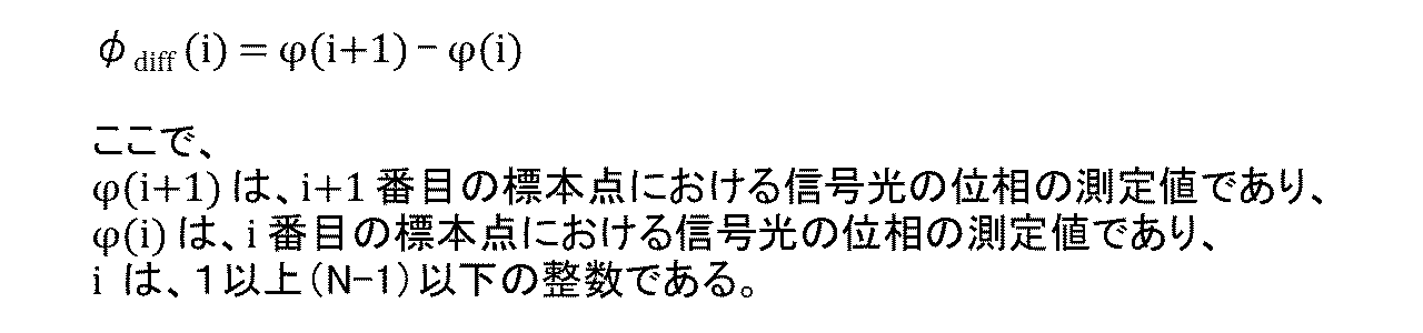
(式4)

(式5)
IQPSK(t)=iI,QPSK(t)+jiQ,QPSK(t)
上記の式において、iI,QPSK(t)は、QPSK変調が施された光信号をコヒーレントヘテロダイン検波して得られたI信号成分に対応する出力電流を示す。iQ,QPSK(t)は、QPSK変調が施された光信号をコヒーレントヘテロダイン検波して得られたQ信号成分に対応する出力電流を示す。
(式6)
arg{IQPSK(t)}4=4(2πfct+θ(t))
上記の式において、fcは、信号光の角周波数fsと局発光の角周波数fLとの差(fs-fL)を表し、ビート周波数と呼ばれる。
(式7)
arg{IQPSK(t)}4/4=2πfct+θ(t)
(式8)

(式9)
σsig=σM/√2
(式10)
σRX 2=σsig 2+σLO 2
(式11)
σLO=σML/√2
一実施形態において、N個の標本点のそれぞれにおける差動位相φdiff(i)は、測定対象となる光(対象光と称される場合がある。)が電気信号に変換された後、当該電気信号が標本化及び量子化されて得られたデジタルデータの信号処理により導出される。例えば、シンボル時間と同一又は略同一の時間間隔で、対象光の位相の時系列データが生成される。時系列データにおいて時間的に隣接する2つのデータの差を算出することで差動位相φdiff(i)が導出される。
実際の通信に使用される信号光の位相雑音が評価される場合、光信号は、変調によるスペクトル成分を有する。そのため、変調成分が測定結果に混入して、光位相雑音の測定に影響を与えることもあり得る。
次に、偏波変動に起因する位相変動の検出原理が説明される。上記の検出原理に基づく偏波変動の検出装置及び検出方法の詳細は、図16~図34を用いて後述される。
(式B-1)
E(t) = [ Ex(t)cos{2πft+φn(t)}kx
+Ey(t)cos{2πft+φn(t)+δ(t)}ky ]
(式B-2)
i = R{E(t)+E(t-τ) }・ {E(t)+E(t-τ) }
(式B-3)

(式B-4)

(式B-5)

(式B-6)

(式B-7)
ipol = -REy 2(t) sin {δ(t)-δ(t-τ)}
上述されたとおり、式B-6において、τは十分に短い時間であり、δ(t)及びδ(t-τ)の差の絶対値は1よりも十分に小さい。このとき、偏波変動に起因する項ipolは、下記の式B-8により近似される。
(式B-8)

(式B-9)
ipol_LPF = -REy 2(t) δ(t)
(式B-10)
Ex2(t) = αE2
(式B-11)
Ey2(t) = (1-α) E2
(式B-12)

この場合、δ(t)及びδ(t-τ)の差の絶対値が1よりも十分に小さいという条件が必ずしも成立しない。そのため、上述された式B-12が必ずしも成立しない。しかしながら、このような場合であっても、式B-7は成立する。そのため、光遅延干渉計に接続された光受信器の出力電流iが、例えば、光受信器に続く増幅器によって増幅される場合、δ(t)はsin関数の制約を受けながら積分される。
ストークスパラメータS0、S1、S2及びS3を用いて表されるポアンカレ球上の点P(S1、S2、S3)が、光の偏波状態を表すことが知られている。Ex(t)及びEy(t)と、δ(t)と、ストークスパラメータS0、S1、S2及びS3との関係は、下記の式B-13、B-14、B-15及びB-16により表される。
(式B-13)




(式B-17)

(式B-18)

(式B-19)

(式B-20)

図1は、通信システム100のシステム構成の一例を概略的に示す。本実施形態においては、光信号送信装置110が出力した信号光が、光伝送路10を伝搬して光信号受信装置120に到達することで、情報信号が伝達される場合を例として、通信システム100の詳細が説明される。
通信システム100の各部は、ハードウエアにより実現されてもよく、ソフトウエアにより実現されてもよく、ハードウエア及びソフトウエアにより実現されてもよい。通信システム100の各部は、その少なくとも一部が、アナログ回路により実現されてもよく、デジタル回路により実現されてもよい。通信システム100の各部は、その少なくとも一部が、単一のサーバによって実現されてもよく、複数のサーバによって実現されてもよい。通信システム100の各部は、その少なくとも一部が、仮想マシン上又はクラウドシステム上で実現されてもよい。通信システム100の各部は、その少なくとも一部が、パーソナルコンピュータ又は携帯端末によって実現されてもよい。携帯端末としては、携帯電話、スマートフォン、PDA、タブレット、ノートブック・コンピュータ又はラップトップ・コンピュータ、ウエアラブル・コンピュータなどが例示される。通信システム100の各部は、ブロックチェーンなどの分散型台帳技術又は分散型ネットワークを利用して、情報を格納してもよい。
(式12)
2πfτ=2nπ+π/2 (ただし、nは整数である。)
(式13)
i=RE2{φn(t)-φn(t-τ)}
上記の式12において、Rは、光受信器350の感度である。Eは、第1入力光及び第2入力光の電界である。φn(t)は、時刻tにおける入力光の位相雑音である。
本実施形態においては、位相雑音評価装置320が、AD変換器360と、信号処理部370とを備える場合を例として、位相雑音評価装置320の一例が説明された。しかしながら、位相雑音評価装置320は、本実施形態に限定されない。他の実施形態において、信号処理部370がAD変換器360の機能を有し、位相雑音評価装置320は、AD変換器360を備えなくてもよい。
本実施形態においては、光位相制御部880が、光受信器350の出力電流の平均値を検出し、当該平均値が0となるように光遅延干渉計340の動作点を設定する場合を例として、光位相制御部880の一例が説明された。しかしながら、光位相制御部880は、本実施形態に限定されない。
図16は、通信システム1600のシステム構成の一例を概略的に示す。本実施形態においては、光信号送信装置110の出力した信号光が、光伝送路10を伝搬して光信号受信装置1620に到達することで、情報信号が伝達される場合を例として、通信システム100の詳細が説明される。
通信システム100の各部と同様、通信システム1600の各部は、ハードウエアにより実現されてもよく、ソフトウエアにより実現されてもよく、ハードウエア及びソフトウエアにより実現されてもよい。通信システム1600を構成する構成要素の少なくとも一部がソフトウエアにより実現される場合、当該ソフトウエアにより実現される構成要素は、一般的な構成の情報処理装置において、当該構成要素に関する動作を規定したプログラムを起動することにより実現されてよい。
本実施形態においては、通信システム1600が、通信システム100と同様の構成に加えて、偏波変動を検出するための構成を備える場合を例として、通信システム1600の詳細が説明された。しかしながら、通信システム1600は、本実施形態に限定されない。他の実施形態において、通信システム1600は、通信システム100の構成の少なくとも一部を備えなくてもよい。例えば、通信システム1600は、振幅雑音評価部230及び位相雑音評価部240の少なくとも一方を備えなくてもよい。
本実施形態においては、状態監視装置1680が光遅延干渉計340を備える場合を例として、状態監視装置1680の詳細が説明された。しかしながら、状態監視装置1680は、本実施形態に限定されない。他の実施形態において、状態監視装置1680は、光遅延干渉計340の代わりに、任意の構成を有する光遅延干渉計を備えてよい。例えば、状態監視装置1680は、光遅延干渉計540、光遅延干渉計640、光遅延干渉計1040、光遅延干渉計1140、光遅延干渉計1240、又は、光遅延干渉計1340を備える。
本実施形態においては、信号処理部1870が、信号処理部370と同様に、ヒストグラム生成部244、標準偏差算出部246及び校正部710を備える場合を例として、信号処理部1870の詳細が説明された。しかしながら、信号処理部1870は、本実施形態に限定されない。
本実施形態においては、偏波変動に関する評価情報が、データテーブル2100に格納される場合を例として、偏波変動に関する評価情報の詳細が説明された。しかしながら、偏波変動に関する評価情報は、本実施形態に限定されない。他の実施形態において、偏波変動に関する評価情報は、偏波変動が検出された1以上の時刻のリストであってもよい。
以下、実験例及び比較実験例を用いて、本発明を具体的に説明する。なお、本発明は、下記の実験例及び比較実験例に限定されるものではない。図23、図24、図25及び図26に、実験例1における各種の測定結果を示す。図27、図28、図29及び図30に、比較実験例1における各種の測定結果を示す。図31、図32、図33及び図34に、実験例2における各種の測定結果を示す。
(偏波状態測定器を用いた測定)
まず、ピエゾ素子に、長さ12.3mの光ファイバ(Corning社製、SMF28e+ファイバ)が4重に巻き付けられたファイバストレッチャー(OPTIPHASE社製、PZ1-SMF4-APC-E)を準備した。光ファイバの一端を、レーザ光発振装置(Pure Photonics社製 PPCL550)に接続した。光ファイバの他端を、偏波状態測定器(Novoptel社製, PM1000 Polarimeter)に接続した。
次に、光ファイバの他端と、偏波状態測定器との接続を解除し、光ファイバの他端を、光遅延干渉計(Optiplex社製、DI-C1EFAM512)の一端に接続した。光遅延干渉計の他端を、バランスド光受信器(Optiplex社製、BR-C0200B1DC)に接続した。バランスド光受信器はローパスフィルタを搭載しており、バランスド光受信器のカットオフ周波数は、150MHzであった。AD変換器(Tektronix社製、オシロスコープ 型番MSO64)を用いて、バランスド光受信器の出力を標本化した。
偏波状態測定器(偏光測定器と称される場合がある。)を用いた測定結果と、光遅延干渉計を用いた測定結果とを比較した。その結果、光遅延干渉計を用いた測定結果は、偏波状態測定器を用いた測定結果とよく一致していた。例えば、ファイバストレッチャーに印加する電圧の大きさ(ピークピーク値)が2Vの場合、偏光測定器により測定されたポアンカレ球上の軌跡の移動両端の座標は、(0.31,0.94,-0.15)及び(0.17,0.98,-0.06)であった。この場合、位相変化量のp-p値は、0.17radであった。一方、光遅延干渉計を用いた測定結果によれば、スペクトル測定結果における140kHz成分のp-p値が0.16radであった。
(偏波状態測定器を用いた測定)
ファイバストレッチャーに印加する電圧の大きさ(ピークピーク値)を200mVに設定した点を除き、実験例1と同様の手順により、ファイバストレッチャー出力光のストークスパラメータを測定した。また、ストークスパラメータの測定結果を用いて、ポアンカレ球上の軌跡の移動角度を導出した。
ファイバストレッチャーに印加する電圧の大きさ(ピークピーク値)を200mVに設定した点を除き、実験例1と同様の手順により、(a)差動位相の大きさに関するヒストグラム、及び、(b)差動位相の大きさの時間変動を示すグラフを作成した。また、(c)差動位相の周波数スペクトルを導出した。
(偏波状態測定器を用いた測定)
まず、光ファイバの一端を、レーザ光発振装置(Pure Photonics社製 型番PPCL550)に接続した。光ファイバの他端を、偏波スクランブラ(Luna Innovations社製、NRT-2500)に接続した。偏波スクランブラの出力端を偏波状態測定器(Novoptel社製, PM1000 Polarimeter)に接続した。
次に、偏波スクランブラの出力端と、偏波状態測定器との接続を解除し、偏波スクランブラの出力端を、光遅延干渉計(Optiplex社製、DI-C1EFAM512)の一端に接続した。光遅延干渉計の他端を、ローパスフィルタ機能を搭載したバランスド光受信器(Optiplex社製、BR-C0200B1DC)に接続した。AD変換器(Tektronix社製、オシロスコープ MSO64)を用いて、バランスド光受信器の出力を標本化した。
[項目A-1]
光伝送路を伝搬した信号光の位相雑音を評価する評価装置であって、
評価期間に含まれる複数の時点のそれぞれにおける入力光の差動位相を示す情報を取得する差動位相情報取得部と、
上記複数の時点のそれぞれにおける上記差動位相のばらつきの度合いを、上記位相雑音を評価するための指標として導出する指標導出部と、
を備え、
上記差動位相は、上記複数の時点のうち時間的に隣接する2つの時点における上記入力光の位相の差を表し、
複数の時点の時間間隔は、略一定であり、上記入力光により伝送される信号のシンボル時間の長さ以下である、
評価装置。
[項目A-2]
上記指標導出部は、上記入力光の差動位相の分散又は標準偏差を、上記指標として導出する、
項目A-1に記載の評価装置。
[項目A-3]
上記信号光により伝送される受信信号を、光信号から電気信号に変換する光電変換部と、
上記電気信号を、アナログ信号からデジタル信号に変換するアナログ-デジタル変換部と、
をさらに備え、
上記アナログ-デジタル変換部は、上記複数の時点のそれぞれに対応する複数のデジタル信号を出力し、
上記差動位相情報取得部は、上記複数のデジタル信号に基づいて、上記複数の時点のそれぞれにおける上記差動位相を示す情報を生成し、
上記指標導出部は、上記複数の時点のそれぞれに対応する上記差動位相のばらつきの度合いを、上記受信信号の位相雑音を評価するための指標として導出し、
上記受信信号は、シンボル時系列が重畳されており、
上記アナログ-デジタル変換部のサンプリングレートは、上記受信信号のシンボル時系列のシンボルレート以上である、
項目A-1又は項目A-2に記載の評価装置。
[項目A-4]
局部発振光を出力する局所光源と、
上記信号光を上記局所光源からの局発光と干渉させて、上記受信信号が複数の信号成分に分離された複数の光信号を出力する光90度ハイブリッドと、
をさらに備え、
上記光電変換部は、
上記光90度ハイブリッドが出力するI信号成分の光信号を電気信号に変換し、
上記光90度ハイブリッドが出力するQ信号成分の光信号を電気信号に変換し、
上記アナログ-デジタル変換部は、
上記複数の時点のそれぞれにおける上記I信号成分の光信号に対応する複数の第1デジタル信号を出力し、
上記複数の時点のそれぞれにおける上記Q信号成分の光信号に対応する複数の第2デジタル信号を出力し、
上記差動位相情報取得部は、
上記複数の第1デジタル信号及び上記複数の第2デジタル信号に基づいて上記受信信号に含まれる変調成分を除去し、
上記複数の時点のそれぞれにおける上記差動位相を示す情報を生成する、
項目A-3に記載の評価装置。
[項目A-5]
上記受信信号の位相雑音の標準偏差の2乗は、上記信号光の位相雑音の標準偏差の2乗と、上記局部発振光のスペクトル線幅による位相雑音の標準偏差の2乗との和の平方根として表される、
項目A-4に記載の評価装置。
[項目A-6]
上記差動位相情報取得部は、
上記入力光が入力される遅延干渉部と、
上記遅延干渉部の出力光を電気信号に変換する光電変換部と、
を有し、
上記遅延干渉部は、
上記入力光を第1入力光及び第2入力光に分岐し、
第1光路を通過した上記第1入力光と、第2光路を通過した上記第2入力光と合波干渉させ、
上記第1光路を通過した上記第1入力光及び上記第2光路を通過した上記第2入力光の遅延時間差τと、上記入力光の周波数fとが、下記の数式FA1の関係を満足するように設定されている、
(数式FA1)
2πfτ=2nπ+π/2 (ただし、nは整数である。)
項目A-1又は項目A-2に記載の評価装置。
[項目A-7]
上記光電変換部が出力した上記電気信号に基づいて、上記遅延干渉部の動作点を調整する調整部をさらに備える、
項目A-6に記載の評価装置。
[項目A-8]
上記差動位相情報取得部は、
上記入力光が入力される導波路と、
上記導波路に隣接して配されるリング共振器と、
上記導波路の出力光を電気信号に変換する光電変換部と、
を有し、
上記リング共振器の入出力特性は、リングの長さがリング媒質中の入力光の波長の整数倍となるように設定される、
項目A-1又は項目A-2に記載の評価装置。
[項目A-9]
上記差動位相情報取得部は、
上記光電変換部が出力した上記電気信号を、アナログ信号からデジタル信号に変換するアナログ-デジタル変換部、
をさらに有し
上記アナログ-デジタル変換部は、上記複数の時点のそれぞれにおける上記差動位相に対応する複数のデジタル信号を出力する、
項目A-6から項目A-8までの何れか一項に記載の評価装置。
[項目A-10]
上記入力光の位相雑音の標準偏差の2乗は、上記差動位相の標準偏差の2乗の1/2倍として表される、
項目A-6から項目A-9までの何れか一項に記載の評価装置。
[項目A-11]
入力光の光電力の測定値を示す情報を取得する光電力情報取得部をさらに備え、
上記指標導出部は
上記入力光の光電力の測定値を用いて、上記入力光の差動位相を規格化し、
上記規格化された上記差動位相を用いて、上記差動位相のばらつきの度合いを導出する、
項目A-1から項目A-10までの何れか一項に記載の評価装置。
[項目A-12]
項目A-1から項目A-11までの何れか一項に記載の評価装置と、
上記信号光により伝送される受信信号を復調し、情報信号を生成する復調部と、
を備える、光受信器。
[項目A-13]
上記信号光を送信する光送信器と、
項目A-12に記載の光受信器と、
を備える、光通信システム。
[項目A-14]
コンピュータを、項目A-1から項目A-11までの何れか一項に記載の評価装置として機能させるためのプログラム。
[項目A-15]
光伝送路を伝播した信号光の位相雑音を評価する評価方法であって、
評価期間に含まれる複数の時点のそれぞれにおける入力光の差動位相を示す情報を取得する差動位相情報取得段階と、
上記複数の時点のそれぞれにおける上記差動位相のばらつきの度合いを、上記位相雑音を評価するための指標として導出する指標導出段階と、
を有し、
上記差動位相は、上記複数の時点のうち時間的に隣接する2つの時点における上記入力光の位相の差を表し、
複数の時点の時間間隔は、略一定であり、上記入力光により伝送される信号のシンボル時間の長さ以下である、
評価方法。
[項目B-1]
光伝送路を伝搬した信号光の偏波変動を検出するための検出装置であって、
1以上の時点のそれぞれにおける、評価対象となる入力光の差動位相を示す情報を取得する差動位相情報取得部と、
上記1以上の時点の少なくとも一部における上記差動位相が予め定められた条件を満たすか否かを判定する判定部と、
を備え、
上記予め定められた条件は、
上記1以上の時点の少なくとも1つにおける上記差動位相の大きさが、予め定められた第1閾値に等しい若しくは上記第1閾値よりも大きいという第1条件、
上記1以上の時点の上記少なくとも一部であって、予め定められた長さを有する期間である評価期間に含まれる複数の時点のうち、当該時点における上記差動位相の大きさが上記第1閾値に等しい若しくは上記第1閾値よりも大きな時点の個数が、予め定められた第2閾値に等しい若しくは上記第2閾値よりも大きいという第2条件、
上記評価期間に含まれる上記複数の時点の個数に対する、上記複数の時点のうち当該時点における上記差動位相の大きさが上記第1閾値に等しい若しくは上記第1閾値よりも大きな時点の個数の割合が、予め定められた第3閾値に等しい又は上記第3閾値よりも大きいという第3条件、
上記1以上の時点のそれぞれにおける上記差動位相の大きさから導出される、ポアンカレ球上の軌跡の変動周波数における移動角度が、予め定められた第4閾値に等しい若しくは上記第4閾値よりも大きいという第4条件、及び、
上記ポアンカレ球上の上記軌跡の上記変動周波数における移動角速度が、予め定められた第5閾値に等しい若しくは上記第5閾値よりも大きいという第5条件、
の少なくとも1つを含む、
検出装置。
[項目B-2]
上記1以上の時点の少なくとも一部における上記差動位相が上記予め定められた条件を満たすと判定された場合に、上記信号光に偏波変動が発生したことを示す情報を出力する出力部をさらに備える、
項目B-1に記載の検出装置。
[項目B-3]
上記差動位相は、上記1以上の時点のうち時間的に隣接する2つの時点における上記入力光の位相の差を表し、
上記1以上の時点の時間間隔は、略一定である、
項目B-1又は項目B-2に記載の検出装置。
[項目B-4]
上記信号光は、
情報信号の伝送に用いられる第1波長の光と、
偏波変動の検出に用いられる第2波長の光と、
を含み、
上記第1波長の値は、上記第2波長の値とは異なり、
上記入力光は、上記第2波長の光である、
項目B-1から項目B-3までの何れか一項に記載の検出装置。
[項目B-5]
上記信号光から上記第2波長の光を分波する分波部をさらに備える、
項目B-4に記載の検出装置。
[項目B-6]
上記差動位相情報取得部は、
上記入力光が入力される遅延干渉部と、
上記遅延干渉部の出力光を電気信号に変換する光電変換部と、
上記光電変換部の出力した上記電気信号が入力され、入力電圧の波形が時間積分された電圧を出力する積分部と、
を有し、
上記遅延干渉部は、
上記入力光を第1入力光及び第2入力光に分岐し、
第1光路を通過した上記第1入力光と、第2光路を通過した上記第2入力光と合波干渉させ、
上記第1光路を通過した上記第1入力光及び上記第2光路を通過した上記第2入力光の遅延時間差τと、上記入力光の周波数fとが、下記の数式FB1の関係を満足するように設定されている、
(数式FB1)
2πfτ=2nπ+π/2 (ただし、nは整数である。)
項目B-1から項目B-5までの何れか一項に記載の検出装置。
[項目B-7]
項目B-1から項目B-6までの何れか一項に記載の検出装置と、
上記信号光により伝送される受信信号を復調し、情報信号を生成する復調部と、
を備える、光受信装置。
[項目B-8]
上記信号光を送信する光送信装置と、
項目B-7に記載の光受信装置と、
を備える、光通信システム。
[項目B-9]
コンピュータを、項目B-1から項目B-6までの何れか一項に記載の検出装置として機能させるためのプログラム。
[項目B-10]
光伝送路を伝搬した信号光の偏波変動を検出するための検出方法であって、
1以上の時点のそれぞれにおける、評価対象となる入力光の差動位相を示す情報を取得する差動位相情報取得段階と、
上記1以上の時点の少なくとも一部における上記差動位相が、予め定められた条件を満たすか否かを判定する判定段階と、
を有し、
上記予め定められた条件は、
上記1以上の時点の少なくとも1つにおける上記差動位相の大きさが、予め定められた第1閾値に等しい若しくは上記第1閾値よりも大きいという第1条件、
上記1以上の時点の上記少なくとも一部であって、予め定められた長さを有する期間である評価期間に含まれる複数の時点のうち、当該時点における上記差動位相の大きさが上記第1閾値に等しい若しくは上記第1閾値よりも大きな時点の個数が、予め定められた第2閾値に等しい若しくは上記第2閾値よりも大きいという第2条件、
上記評価期間に含まれる上記複数の時点の個数に対する、上記複数の時点のうち当該時点における上記差動位相の大きさが上記第1閾値に等しい若しくは上記第1閾値よりも大きな時点の個数の割合が、予め定められた第3閾値に等しい又は上記第3閾値よりも大きいという第3条件、
上記1以上の時点のそれぞれにおける上記差動位相の大きさから導出される、ポアンカレ球上の軌跡の変動周波数における移動角度が、予め定められた第4閾値に等しい若しくは上記第4閾値よりも大きいという第4条件、及び、
上記ポアンカレ球上の上記軌跡の上記変動周波数における移動角速度が、予め定められた第5閾値に等しい若しくは上記第5閾値よりも大きいという第5条件、
の少なくとも1つを含む、
検出方法。
Claims (10)
- 光伝送路を伝搬した信号光の偏波変動を検出するための検出装置であって、
1以上の時点のそれぞれにおける、評価対象となる入力光の差動位相を示す情報を取得する差動位相情報取得部と、
前記1以上の時点の少なくとも一部における前記差動位相が予め定められた条件を満たすか否かを判定する判定部と、
を備え、
前記予め定められた条件は、
前記1以上の時点の少なくとも1つにおける前記差動位相の大きさが、予め定められた第1閾値に等しい若しくは前記第1閾値よりも大きいという第1条件、
前記1以上の時点の前記少なくとも一部であって、予め定められた長さを有する期間である評価期間に含まれる複数の時点のうち、当該時点における前記差動位相の大きさが前記第1閾値に等しい若しくは前記第1閾値よりも大きな時点の個数が、予め定められた第2閾値に等しい若しくは前記第2閾値よりも大きいという第2条件、
前記評価期間に含まれる前記複数の時点の個数に対する、前記複数の時点のうち当該時点における前記差動位相の大きさが前記第1閾値に等しい若しくは前記第1閾値よりも大きな時点の個数の割合が、予め定められた第3閾値に等しい又は前記第3閾値よりも大きいという第3条件、
前記1以上の時点のそれぞれにおける前記差動位相の大きさから導出される、ポアンカレ球上の軌跡の変動周波数における移動角度が、予め定められた第4閾値に等しい若しくは前記第4閾値よりも大きいという第4条件、及び、
前記ポアンカレ球上の前記軌跡の前記変動周波数における移動角速度が、予め定められた第5閾値に等しい若しくは前記第5閾値よりも大きいという第5条件、
の少なくとも1つを含む、
検出装置。 - 前記1以上の時点の少なくとも一部における前記差動位相が前記予め定められた条件を満たすと判定された場合に、前記信号光に偏波変動が発生したことを示す情報を出力する出力部をさらに備える、
請求項1に記載の検出装置。 - 前記差動位相は、前記1以上の時点のうち時間的に隣接する2つの時点における前記入力光の位相の差を表し、
前記1以上の時点の時間間隔は、略一定である、
請求項1に記載の検出装置。 - 前記信号光は、
情報信号の伝送に用いられる第1波長の光と、
偏波変動の検出に用いられる第2波長の光と、
を含み、
前記第1波長の値は、前記第2波長の値とは異なり、
前記入力光は、前記第2波長の光である、
請求項1に記載の検出装置。 - 前記信号光から前記第2波長の光を分波する分波部をさらに備える、
請求項4に記載の検出装置。 - 前記差動位相情報取得部は、
前記入力光が入力される遅延干渉部と、
前記遅延干渉部の出力光を電気信号に変換する光電変換部と、
前記光電変換部の出力した前記電気信号が入力され、入力電圧の波形が時間積分された電圧を出力する積分部と、
を有し、
前記遅延干渉部は、
前記入力光を第1入力光及び第2入力光に分岐し、
第1光路を通過した前記第1入力光と、第2光路を通過した前記第2入力光と合波干渉させ、
前記第1光路を通過した前記第1入力光及び前記第2光路を通過した前記第2入力光の遅延時間差τと、前記入力光の周波数fとが、下記の数式1の関係を満足するように設定されている、
(数式1)
2πfτ=2nπ+π/2 (ただし、nは整数である。)
請求項1に記載の検出装置。 - 請求項1から請求項6までの何れか一項に記載の検出装置と、
前記信号光により伝送される受信信号を復調し、情報信号を生成する復調部と、
を備える、光受信装置。 - 前記信号光を送信する光送信装置と、
請求項7に記載の光受信装置と、
を備える、光通信システム。 - コンピュータを、請求項1から請求項6までの何れか一項に記載の検出装置として機能させるためのプログラム。
- 光伝送路を伝搬した信号光の偏波変動を検出するための検出方法であって、
1以上の時点のそれぞれにおける、評価対象となる入力光の差動位相を示す情報を取得する差動位相情報取得段階と、
前記1以上の時点の少なくとも一部における前記差動位相が、予め定められた条件を満たすか否かを判定する判定段階と、
を有し、
前記予め定められた条件は、
前記1以上の時点の少なくとも1つにおける前記差動位相の大きさが、予め定められた第1閾値に等しい若しくは前記第1閾値よりも大きいという第1条件、
前記1以上の時点の前記少なくとも一部であって、予め定められた長さを有する期間である評価期間に含まれる複数の時点のうち、当該時点における前記差動位相の大きさが前記第1閾値に等しい若しくは前記第1閾値よりも大きな時点の個数が、予め定められた第2閾値に等しい若しくは前記第2閾値よりも大きいという第2条件、
前記評価期間に含まれる前記複数の時点の個数に対する、前記複数の時点のうち当該時点における前記差動位相の大きさが前記第1閾値に等しい若しくは前記第1閾値よりも大きな時点の個数の割合が、予め定められた第3閾値に等しい又は前記第3閾値よりも大きいという第3条件、
前記1以上の時点のそれぞれにおける前記差動位相の大きさから導出される、ポアンカレ球上の軌跡の変動周波数における移動角度が、予め定められた第4閾値に等しい若しくは前記第4閾値よりも大きいという第4条件、及び、
前記ポアンカレ球上の前記軌跡の前記変動周波数における移動角速度が、予め定められた第5閾値に等しい若しくは前記第5閾値よりも大きいという第5条件、
の少なくとも1つを含む、
検出方法。
Priority Applications (4)
| Application Number | Priority Date | Filing Date | Title |
|---|---|---|---|
| CN202280058568.1A CN117882317B (zh) | 2021-12-24 | 2022-12-22 | 检测装置、光接收装置、光通信系统、存储介质以及检测方法 |
| JP2023569554A JP7478401B2 (ja) | 2021-12-24 | 2022-12-22 | 検出装置、光受信装置、光通信システム、プログラム及び検出方法 |
| EP22911378.2A EP4401338A4 (en) | 2021-12-24 | 2022-12-22 | DETECTION DEVICE, OPTICAL RECEIVING DEVICE, OPTICAL COMMUNICATION SYSTEM, PROGRAM AND DETECTION METHOD |
| US18/589,426 US12341555B2 (en) | 2021-12-24 | 2024-02-28 | Detection device, optical reception device, optical communication system, program, and detection method |
Applications Claiming Priority (2)
| Application Number | Priority Date | Filing Date | Title |
|---|---|---|---|
| PCT/JP2021/048423 WO2023119673A1 (ja) | 2021-12-24 | 2021-12-24 | 評価装置、光受信器、光通信システム、プログラム及び評価方法 |
| JPPCT/JP2021/048423 | 2021-12-24 |
Related Parent Applications (1)
| Application Number | Title | Priority Date | Filing Date |
|---|---|---|---|
| PCT/JP2021/048423 Continuation WO2023119673A1 (ja) | 2021-12-24 | 2021-12-24 | 評価装置、光受信器、光通信システム、プログラム及び評価方法 |
Related Child Applications (1)
| Application Number | Title | Priority Date | Filing Date |
|---|---|---|---|
| US18/589,426 Continuation US12341555B2 (en) | 2021-12-24 | 2024-02-28 | Detection device, optical reception device, optical communication system, program, and detection method |
Publications (1)
| Publication Number | Publication Date |
|---|---|
| WO2023120676A1 true WO2023120676A1 (ja) | 2023-06-29 |
Family
ID=86901760
Family Applications (2)
| Application Number | Title | Priority Date | Filing Date |
|---|---|---|---|
| PCT/JP2021/048423 Ceased WO2023119673A1 (ja) | 2021-12-24 | 2021-12-24 | 評価装置、光受信器、光通信システム、プログラム及び評価方法 |
| PCT/JP2022/047485 Ceased WO2023120676A1 (ja) | 2021-12-24 | 2022-12-22 | 検出装置、光受信装置、光通信システム、プログラム及び検出方法 |
Family Applications Before (1)
| Application Number | Title | Priority Date | Filing Date |
|---|---|---|---|
| PCT/JP2021/048423 Ceased WO2023119673A1 (ja) | 2021-12-24 | 2021-12-24 | 評価装置、光受信器、光通信システム、プログラム及び評価方法 |
Country Status (5)
| Country | Link |
|---|---|
| US (1) | US12341555B2 (ja) |
| EP (1) | EP4401338A4 (ja) |
| JP (1) | JP7478401B2 (ja) |
| CN (1) | CN117882317B (ja) |
| WO (2) | WO2023119673A1 (ja) |
Cited By (4)
| Publication number | Priority date | Publication date | Assignee | Title |
|---|---|---|---|---|
| US20250015894A1 (en) * | 2023-06-22 | 2025-01-09 | Meiji University | Control device, compensation device, program, and control method |
| US12341555B2 (en) | 2021-12-24 | 2025-06-24 | MEIJI UNIVERSITY & SoftBank Corp. | Detection device, optical reception device, optical communication system, program, and detection method |
| WO2025248738A1 (ja) * | 2024-05-30 | 2025-12-04 | 学校法人明治大学 | 検出装置、光信号受信装置、光通信システム、プログラム、及び検出方法 |
| WO2025248737A1 (ja) * | 2024-05-30 | 2025-12-04 | 学校法人明治大学 | 検出装置、光信号受信装置、光通信システム、プログラム、及び検出方法 |
Citations (3)
| Publication number | Priority date | Publication date | Assignee | Title |
|---|---|---|---|---|
| JP2006352892A (ja) * | 2005-06-17 | 2006-12-28 | Jds Uniphase Corp | パルス光信号を特徴付ける装置および方法 |
| JP2018207181A (ja) * | 2017-05-30 | 2018-12-27 | 富士通株式会社 | 光伝送装置および光伝送方法 |
| WO2021205786A1 (ja) * | 2020-04-07 | 2021-10-14 | 日本電気株式会社 | 偏波変動推定装置及び偏波変動推定方法 |
Family Cites Families (56)
| Publication number | Priority date | Publication date | Assignee | Title |
|---|---|---|---|---|
| US4442350A (en) * | 1981-08-17 | 1984-04-10 | The United States Of America As Represented By The Secretary Of The Navy | Fiber optic sensor with enhanced immunity to random environmental perturbations |
| GB8829546D0 (en) * | 1988-12-19 | 1989-02-08 | British Telecomm | Non-linear interferometer |
| CA2086704C (en) * | 1993-01-05 | 2002-06-04 | Robert J. Inkol | Method for evaluating similarity of signals having a carrier frequency offset |
| JP3415267B2 (ja) | 1993-06-21 | 2003-06-09 | 日本電信電話株式会社 | 光信号処理器の設計方法および製造方法 |
| GB2286937B (en) * | 1994-02-26 | 1998-06-10 | Northern Telecom Ltd | Spectral polarisation separator |
| JPH0918409A (ja) | 1995-06-28 | 1997-01-17 | Nippon Telegr & Teleph Corp <Ntt> | 光タイミングジッタ補償回路 |
| JP3286885B2 (ja) * | 1995-11-07 | 2002-05-27 | 三菱電機株式会社 | タイミング再生手段及びダイバーシティ通信装置 |
| JP3216985B2 (ja) * | 1996-03-08 | 2001-10-09 | 三菱電機株式会社 | 回線制御装置 |
| US5661433A (en) * | 1996-06-27 | 1997-08-26 | Motorola, Inc. | Digital FM demodulator |
| US6111910A (en) * | 1997-12-11 | 2000-08-29 | Nortel Networks Corporation | Maximal correlation symbol estimation demodulator |
| US6249518B1 (en) * | 1998-08-07 | 2001-06-19 | Nortel Networks Limited | TDMA single antenna co-channel interference cancellation |
| US6590520B1 (en) * | 2002-02-04 | 2003-07-08 | Lockheed Martin Corporation | Method and system for determining air turbulence using bi-static measurements |
| WO2006074502A1 (en) | 2005-01-11 | 2006-07-20 | Future Fibre Technologies Pty Ltd | Apparatus and method for using a counter-propagating signal method for locating events |
| US7826811B2 (en) * | 2005-11-10 | 2010-11-02 | Panasonic Corporation | Phase modulation apparatus and wireless communication apparatus |
| US20080025733A1 (en) | 2006-06-27 | 2008-01-31 | Technion Research & Development Foundation Ltd. | Optical differential phase shift keying receivers with multi-symbol decision feedback-based electro-optic front-end processing |
| DE102006030915B4 (de) * | 2006-06-29 | 2008-04-10 | Fraunhofer-Gesellschaft zur Förderung der angewandten Forschung e.V. | Optischer Empfänger für den Empfang eines Signales mit M-wertiger sternförmiger Quadratur-Amplitudenmodulation mit differenzieller Phasenkodierung und dessen Verwendung |
| JP4620642B2 (ja) * | 2006-07-31 | 2011-01-26 | 富士通株式会社 | 多値変調受信装置 |
| CN101507149B (zh) * | 2006-09-26 | 2011-12-28 | 株式会社日立制作所 | 光场接收器以及光传输系统 |
| ES2338715T3 (es) * | 2006-10-06 | 2010-05-11 | Acterna Llc | Comprobacion de enlaces amplificados opticamente mediante señales de prueba de multiplexacion por division de tiempo. |
| JP2008197621A (ja) * | 2007-01-16 | 2008-08-28 | Anritsu Corp | 光位相変調評価装置 |
| CN101442364B (zh) * | 2007-11-19 | 2011-10-19 | 富士通株式会社 | 光相干接收机、光相干接收机用频差估计装置及方法 |
| JP2009198364A (ja) | 2008-02-22 | 2009-09-03 | Fujitsu Ltd | 光ファイバ伝送路の特性および光信号の品質をモニタするモニタ回路 |
| JP5044499B2 (ja) * | 2008-07-25 | 2012-10-10 | アンリツ株式会社 | 光位相変調信号評価装置及び光位相変調信号評価方法 |
| US8184756B2 (en) * | 2008-12-18 | 2012-05-22 | Viasat, Inc. | Symbol timing acquisition using early-late interpolation |
| JP5444877B2 (ja) * | 2009-06-24 | 2014-03-19 | 富士通株式会社 | デジタルコヒーレント受信器 |
| US9100126B2 (en) * | 2009-11-24 | 2015-08-04 | Nec Corporation | Optical reception device and optical reception control method |
| KR101068414B1 (ko) * | 2010-01-08 | 2011-09-29 | 한국과학기술원 | 광신호의 성능 감시 방법 |
| JP5409479B2 (ja) * | 2010-03-29 | 2014-02-05 | 日立コンシューマエレクトロニクス株式会社 | 光情報再生装置、光情報記録装置及び情報記録方法 |
| JP2012015675A (ja) * | 2010-06-30 | 2012-01-19 | Nec Corp | Wdm信号光の監視装置 |
| EP2628261B1 (en) * | 2010-10-14 | 2018-04-04 | RWTH Aachen | Broadband optical phase detection and phase noise removal with an optical resonator |
| JP5567126B2 (ja) * | 2010-10-18 | 2014-08-06 | 株式会社フジクラ | 波長分散測定装置及びそれを用いた波長分散測定方法 |
| JP2012105039A (ja) * | 2010-11-10 | 2012-05-31 | Renesas Electronics Corp | ラジオ受信機及びラジオ受信方法 |
| JP5720425B2 (ja) * | 2011-05-31 | 2015-05-20 | 富士通株式会社 | デジタルコヒーレント受信機及び位相制御方法 |
| JP5899849B2 (ja) * | 2011-11-16 | 2016-04-06 | 富士通株式会社 | 光伝送システム、光伝送装置、信号調整プログラム及び信号調整方法 |
| WO2013136716A1 (ja) * | 2012-03-14 | 2013-09-19 | 日本電気株式会社 | 光位相偏差・光搬送波周波数偏差補償装置および光位相偏差・光搬送波周波数偏差補償方法 |
| JP6015291B2 (ja) * | 2012-09-24 | 2016-10-26 | 沖電気工業株式会社 | 光信号品質評価装置及び光信号品質評価方法 |
| US20150116162A1 (en) * | 2013-10-28 | 2015-04-30 | Skycross, Inc. | Antenna structures and methods thereof for determining a frequency offset based on a differential magnitude |
| EP3142269A4 (en) * | 2014-05-08 | 2017-10-04 | Mitsubishi Electric Corporation | Optical transmission method and optical transmission system |
| JP6519999B2 (ja) * | 2014-07-16 | 2019-05-29 | 富士通株式会社 | 光送信装置及び検出装置 |
| JP6485095B2 (ja) * | 2015-02-18 | 2019-03-20 | 富士通株式会社 | 光伝送装置、光伝送システム、及び、偏波依存損失モニタ |
| EP3316500A1 (en) * | 2015-06-29 | 2018-05-02 | Mitsubishi Electric Corporation | Optical transmitter, optical receiver, optical transmission system, and optical transmission method |
| JP2017028359A (ja) | 2015-07-16 | 2017-02-02 | 富士通株式会社 | 光受信装置およびタップ係数の更新方法 |
| JP6578199B2 (ja) * | 2015-12-16 | 2019-09-18 | 日本ルメンタム株式会社 | 光受信モジュール |
| US9755864B1 (en) | 2016-03-07 | 2017-09-05 | Huawei Technologies Co., Ltd | Fractionally spaced adaptive equalizer with non-integer sampling |
| CN109845144B (zh) | 2016-10-28 | 2022-07-22 | 日本电信电话株式会社 | 光接收机、光接收方法和光通信系统 |
| JP6806641B2 (ja) | 2017-07-18 | 2021-01-06 | 日本電信電話株式会社 | 空間多重光伝送路評価装置及び方法 |
| JP7013802B2 (ja) * | 2017-11-09 | 2022-02-15 | 日立金属株式会社 | 光ケーブル監視システム |
| JP7057506B2 (ja) | 2018-09-11 | 2022-04-20 | 日本電信電話株式会社 | デジタルコヒーレント受信器及びデジタルコヒーレント受信方法 |
| CN110971294B (zh) | 2018-09-28 | 2023-02-17 | 富士通株式会社 | 光链路导致的偏振态变化监测装置及方法、光接收机 |
| JP2020170902A (ja) | 2019-04-01 | 2020-10-15 | 富士通株式会社 | 光送受信機、偏波変動モニタ方法、および通信プログラム |
| JP6876099B2 (ja) | 2019-06-21 | 2021-05-26 | Nttエレクトロニクス株式会社 | 適応等化器、適応等化方法及び光通信システム |
| JP7206528B2 (ja) * | 2019-08-01 | 2023-01-18 | 日本電信電話株式会社 | 光波長合分波回路 |
| WO2021038677A1 (ja) | 2019-08-26 | 2021-03-04 | 三菱電機株式会社 | 受信器 |
| EP3855138B1 (en) * | 2020-01-24 | 2025-07-23 | Nokia Solutions and Networks Oy | Fiber phase sensing using a ladder topology |
| US20220221583A1 (en) | 2020-04-13 | 2022-07-14 | Imra America, Inc. | Ultra-low phase noise millimeter-wave oscillator and methods to characterize same |
| WO2023119673A1 (ja) * | 2021-12-24 | 2023-06-29 | 学校法人明治大学 | 評価装置、光受信器、光通信システム、プログラム及び評価方法 |
-
2021
- 2021-12-24 WO PCT/JP2021/048423 patent/WO2023119673A1/ja not_active Ceased
-
2022
- 2022-12-22 JP JP2023569554A patent/JP7478401B2/ja active Active
- 2022-12-22 EP EP22911378.2A patent/EP4401338A4/en active Pending
- 2022-12-22 CN CN202280058568.1A patent/CN117882317B/zh active Active
- 2022-12-22 WO PCT/JP2022/047485 patent/WO2023120676A1/ja not_active Ceased
-
2024
- 2024-02-28 US US18/589,426 patent/US12341555B2/en active Active
Patent Citations (3)
| Publication number | Priority date | Publication date | Assignee | Title |
|---|---|---|---|---|
| JP2006352892A (ja) * | 2005-06-17 | 2006-12-28 | Jds Uniphase Corp | パルス光信号を特徴付ける装置および方法 |
| JP2018207181A (ja) * | 2017-05-30 | 2018-12-27 | 富士通株式会社 | 光伝送装置および光伝送方法 |
| WO2021205786A1 (ja) * | 2020-04-07 | 2021-10-14 | 日本電気株式会社 | 偏波変動推定装置及び偏波変動推定方法 |
Non-Patent Citations (16)
| Title |
|---|
| "High spectral density optical communication technologies", 2010, SPRINGER-VERLAG |
| J. CHENG ET AL.: "Relative phase noise induced impairment in M-ary phase shift-keying coherent optical communication system using distributed fiber Raman amplifier", OPTICS LETTERS, vol. 38, no. 7, 2013, pages 1055 - 1057, XP001581051, DOI: http://dx.doi.org/10.1364/OL.38.001055 |
| J. GARNETG. PANDRAUD: "C- and L-band planar delay interferometer for DPSK decoders", IEEE PHOTONICS TECHNOLOGY LETTERS, vol. 17, no. 6, 2005, pages 1217 - 1219, XP011132274, DOI: 10.1109/LPT.2005.846921 |
| J. P. GORDONL. F. MULLENAUER: "Phase noise in photonic communications systems using linear amplifiers", OPTICS LETTERS, vol. 15, no. 23, 1990, pages 1351 - 1353, XP002973594, DOI: 10.1364/OL.15.001351 |
| K. KIKUCHI: "Effect of 1/f-type FM noise on semiconductor-laser linewidth residual in high-power limit", IEEE JOURNAL OF QUANTUM ELECTRONICS, vol. 25, no. 4, 1989, pages 684 - 688, XP000026569, DOI: 10.1109/3.17331 |
| K. VOIGT ET AL.: "Performance of 40-Gb/s DPSK demodulator in SOI-technology", IEEE PHOTONICS TECHNOLOGY LETTERS, vol. 20, no. 8, 2008, pages 614 - 616, XP011206298 |
| M. BORODITSKYM. BRODSKYN.J. FRIGOP. MAGILLH. ROSENFELDT: "Polarization dynamics in installed fiberoptic systems", 2005 IEEE LEOS ANNUAL MEETING, October 2005 (2005-10-01) |
| P.M. KRUMMRICHE.-D. SCHMIDTW. WEIERSHAUSENA. MATTHEUS: "Field trial results on statistics of fast polarization changes in long haul WDM transmission systems", OFC2005, March 2005 (2005-03-01) |
| R. ULRICHA. SIMON: "Polarization optics of twisted single-mode fibers", APPLIED OPTICS, vol. 18, no. 13, July 1979 (1979-07-01), pages 2241 - 2251, XP000669902, DOI: 10.1364/AO.18.002241 |
| S. RYU: "Signal linewidth broadening due to nonlinear Kerr effect in long-haul coherent systems using cascaded optical amplifiers", IEEE JOURNAL OF LIGHTWAVE TECHNOLOGY, vol. 10, no. 10, 1992, pages 1450 - 1457 |
| S. SUZUKI ET AL.: "Integrated-optic double-ring resonators with a wide free spectral range of 100 GHz", IEEE JOURNAL OF LIGHTWAVE TECHNOLOGY, vol. 13, no. 8, 1995, pages 1766 - 1771, XP000537135, DOI: 10.1109/50.405322 |
| S. ZHANG ET AL.: "Bit-error rate performance of coherent optical M-ary PSK/QAM using decision-aided maximum likelihood phase estimation", OPTICS EXPRESS, vol. 18, no. 12, 2010, pages 12088 - 12103 |
| See also references of EP4401338A4 |
| T. KOMINATO: "Ring resonators composed of GeO2-doped silica waveguides", IEEE JOURNAL OF LIGHTWAVE TECHNOLOGY, vol. 10, no. 12, 1992, pages 1781 - 1788, XP000367882, DOI: 10.1109/50.202829 |
| T. PFAU ET AL.: "Hardware-efficient coherent digital receiver concept with feedforward carrier recovery for M-QAM constellations", IEEE JOURNAL OF LIGHTWAVE TECHNOLOGY, vol. 27, no. 8, 2009, pages 989 - 999, XP011255446 |
| W. BOGAERTS ET AL.: "Silicon microring resonators", LASER AND PHOTONICS REVIEWS, vol. 6, no. 1, 2012, pages 47 - 73 |
Cited By (5)
| Publication number | Priority date | Publication date | Assignee | Title |
|---|---|---|---|---|
| US12341555B2 (en) | 2021-12-24 | 2025-06-24 | MEIJI UNIVERSITY & SoftBank Corp. | Detection device, optical reception device, optical communication system, program, and detection method |
| US20250015894A1 (en) * | 2023-06-22 | 2025-01-09 | Meiji University | Control device, compensation device, program, and control method |
| US12375178B2 (en) * | 2023-06-22 | 2025-07-29 | Meiji University | Control device, compensation device, program, and control method |
| WO2025248738A1 (ja) * | 2024-05-30 | 2025-12-04 | 学校法人明治大学 | 検出装置、光信号受信装置、光通信システム、プログラム、及び検出方法 |
| WO2025248737A1 (ja) * | 2024-05-30 | 2025-12-04 | 学校法人明治大学 | 検出装置、光信号受信装置、光通信システム、プログラム、及び検出方法 |
Also Published As
| Publication number | Publication date |
|---|---|
| US20240214067A1 (en) | 2024-06-27 |
| JP7478401B2 (ja) | 2024-05-07 |
| EP4401338A4 (en) | 2025-09-03 |
| CN117882317B (zh) | 2025-05-02 |
| WO2023119673A1 (ja) | 2023-06-29 |
| JPWO2023120676A1 (ja) | 2023-06-29 |
| EP4401338A1 (en) | 2024-07-17 |
| CN117882317A (zh) | 2024-04-12 |
| US12341555B2 (en) | 2025-06-24 |
Similar Documents
| Publication | Publication Date | Title |
|---|---|---|
| JP7478401B2 (ja) | 検出装置、光受信装置、光通信システム、プログラム及び検出方法 | |
| JPH10271066A (ja) | 光信号の伝送方法、光伝送システム、および光伝送システムの監視装置 | |
| US8229254B2 (en) | Systems and methods for polarization mode dispersion mitigation | |
| US10148350B2 (en) | Method and system for differentiating macro-bend losses from splice and connector losses in fiber-optic links | |
| US12136997B2 (en) | Polarization-fluctuation estimating device and polarization-fluctuation estimating method | |
| US12375178B2 (en) | Control device, compensation device, program, and control method | |
| US20080019704A1 (en) | Interferometer-based chromatic dispersion monitor | |
| CN107835053A (zh) | 一种高精度瞬时微波频率测量装置 | |
| WO2017114369A1 (zh) | 一种监测偏振模色散的方法及装置 | |
| Sun et al. | An ameliorated positioning scheme for optical fiber interferometer-based vibration sensors in perimeter security monitoring application | |
| Hazim et al. | Developments in optical fiber network fault detection methods: An extensive analysis | |
| Wu et al. | QPSK training sequence-based both OSNR and chromatic dispersion monitoring in DWDM systems | |
| US20100067903A1 (en) | Interferometric optical signal-to-noise ratio measurement using a calibration factor | |
| Hazim et al. | Developments in optical fiber network fault detection methods: an extensive analysis | |
| US9768876B1 (en) | Method of suppressing polarization-dependent loss in polarization-modulated photonic links | |
| WO2025248738A1 (ja) | 検出装置、光信号受信装置、光通信システム、プログラム、及び検出方法 | |
| CN109004983A (zh) | 一种基于相位到强度调制转换原理的精确传感方法 | |
| CN113078946B (zh) | 一种光信噪比监测方法及其系统 | |
| JP2019022102A (ja) | 光受信機の検査方法及び光受信機の検査装置 | |
| Precious et al. | Experimental Evaluation of PMD Effects in NRZ and QAM-modulated High-speed Optical Systems in Abuja, Nigeria | |
| Ryu | Optical phase noise and polarization fluctuation measurement with delay interferometer | |
| CN120521708B (zh) | 一种基于色散的单向光纤通信与分布式传感深度融合定位方法、系统、终端及存储介质 | |
| WO2025248737A1 (ja) | 検出装置、光信号受信装置、光通信システム、プログラム、及び検出方法 | |
| Shan et al. | SOP Monitoring Using Time-Frequency Feature Extraction of the Polarization Tributary Powers | |
| Schanner et al. | Low-Complexity Method for Optical Fiber Nonlinear Coefficient Measurement |
Legal Events
| Date | Code | Title | Description |
|---|---|---|---|
| 121 | Ep: the epo has been informed by wipo that ep was designated in this application |
Ref document number: 22911378 Country of ref document: EP Kind code of ref document: A1 |
|
| WWE | Wipo information: entry into national phase |
Ref document number: 2023569554 Country of ref document: JP |
|
| WWE | Wipo information: entry into national phase |
Ref document number: 202280058568.1 Country of ref document: CN |
|
| WWE | Wipo information: entry into national phase |
Ref document number: 2022911378 Country of ref document: EP |
|
| ENP | Entry into the national phase |
Ref document number: 2022911378 Country of ref document: EP Effective date: 20240408 |
|
| NENP | Non-entry into the national phase |
Ref country code: DE |
|
| WWG | Wipo information: grant in national office |
Ref document number: 202280058568.1 Country of ref document: CN |