WO2023210317A1 - Carte de circuit imprimé, isolateur numérique ou transformateur, et procédé de fabrication de carte de circuit imprimé - Google Patents
Carte de circuit imprimé, isolateur numérique ou transformateur, et procédé de fabrication de carte de circuit imprimé Download PDFInfo
- Publication number
- WO2023210317A1 WO2023210317A1 PCT/JP2023/014499 JP2023014499W WO2023210317A1 WO 2023210317 A1 WO2023210317 A1 WO 2023210317A1 JP 2023014499 W JP2023014499 W JP 2023014499W WO 2023210317 A1 WO2023210317 A1 WO 2023210317A1
- Authority
- WO
- WIPO (PCT)
- Prior art keywords
- circuit board
- forming
- insulating layer
- coil
- core
- Prior art date
- Legal status (The legal status is an assumption and is not a legal conclusion. Google has not performed a legal analysis and makes no representation as to the accuracy of the status listed.)
- Ceased
Links
Images


Classifications
-
- H—ELECTRICITY
- H01—ELECTRIC ELEMENTS
- H01F—MAGNETS; INDUCTANCES; TRANSFORMERS; SELECTION OF MATERIALS FOR THEIR MAGNETIC PROPERTIES
- H01F17/00—Fixed inductances of the signal type
- H01F17/04—Fixed inductances of the signal type with magnetic core
-
- H—ELECTRICITY
- H01—ELECTRIC ELEMENTS
- H01F—MAGNETS; INDUCTANCES; TRANSFORMERS; SELECTION OF MATERIALS FOR THEIR MAGNETIC PROPERTIES
- H01F30/00—Fixed transformers not covered by group H01F19/00
- H01F30/06—Fixed transformers not covered by group H01F19/00 characterised by the structure
- H01F30/10—Single-phase transformers
-
- H—ELECTRICITY
- H05—ELECTRIC TECHNIQUES NOT OTHERWISE PROVIDED FOR
- H05K—PRINTED CIRCUITS; CASINGS OR CONSTRUCTIONAL DETAILS OF ELECTRIC APPARATUS; MANUFACTURE OF ASSEMBLAGES OF ELECTRICAL COMPONENTS
- H05K1/00—Printed circuits
- H05K1/02—Details
-
- H—ELECTRICITY
- H05—ELECTRIC TECHNIQUES NOT OTHERWISE PROVIDED FOR
- H05K—PRINTED CIRCUITS; CASINGS OR CONSTRUCTIONAL DETAILS OF ELECTRIC APPARATUS; MANUFACTURE OF ASSEMBLAGES OF ELECTRICAL COMPONENTS
- H05K1/00—Printed circuits
- H05K1/16—Printed circuits incorporating printed electric components, e.g. printed resistors, capacitors or inductors
Definitions
- the present invention relates to a circuit board, a digital isolator or a transformer, and a method for manufacturing a circuit board.
- Patent Document 1 describes a thin magnetic component in which a coil conductor is formed.
- a first conductor is provided in a slit-like groove on one side of the magnetic substrate, and a second conductor is provided in a slit-like groove on the other side of the magnetic substrate.
- the first conductor and the second conductor are connected by a connecting conductor provided in the through hole of the magnetic substrate.
- the inventors of the present invention considered developing other magnetic components using small coils.
- the inventors of the present invention considered developing a digital isolator or transformer using two coils.
- dielectric strength cannot be maintained. Therefore, it is difficult to miniaturize digital isolators or transformers.
- An object of the present invention is to provide a circuit board, a digital isolator, or a transformer that can be used as a magnetic component and can be miniaturized, and a method for manufacturing the circuit board.
- a circuit board includes a core formed of a magnetic material and having a thickness of 10 ⁇ m or more and 300 ⁇ m or less, an insulating layer provided around the core, and a core wound around the core via the insulating layer. The rotated first coil and second coil, the first wiring and second wiring connected to the first coil, and the third wiring and fourth wiring connected to the second coil. Equipped with.
- the magnetic coupling between the first coil and the second coil is large, it becomes possible to arrange the first coil and the second coil apart from each other. This maintains the dielectric strength between the first coil and the second coil. As a result, it is possible to downsize the circuit board while configuring the circuit board as a magnetic component.
- Each of the first coil, second coil, first wiring, second wiring, third wiring, and fourth wiring may have a rectangular cross section.
- each of the first coil, second coil, first wiring, second wiring, third wiring, and fourth wiring can be easily formed using a wiring circuit board forming technique. Can be done.
- the first coil and the second coil may be arranged with a distance of 10 ⁇ m or more. In this case, the dielectric strength voltage between the first coil and the second coil can be sufficiently maintained.
- the core may be formed of a ferromagnetic material. In this case, the magnetic coupling between the first coil and the second coil can be further increased.
- the core may include silicon steel, iron, or permalloy. In this case, the magnetic coupling between the first coil and the second coil can be easily increased.
- the first coil and the second coil may be magnetically coupled and may transmit electrical signals or power while being electrically insulated from each other.
- the circuit board can be used as a digital isolator or transformer.
- a digital isolator or transformer according to another aspect of the present invention includes a circuit board according to one aspect of the present invention. Since this digital isolator or transformer includes the above-mentioned circuit board, it can be made small while being constructed as a ceramic component.
- a method for manufacturing a circuit board includes preparing a core made of a magnetic material and having a thickness of 10 ⁇ m or more and 300 ⁇ m or less, and forming a first insulating layer around the core. and forming a conductor layer, the conductor layer being connected to the first coil and the second coil wound around the core through the first insulating layer.
- the coil includes a first wiring and a second wiring connected to each other, and a third wiring and a fourth wiring connected to the second coil.
- Forming the first insulating layer means forming a first portion of the first insulating layer on one surface of the core, and forming a first portion of the first insulating layer on the other surface of the core, which is connected to the first portion.
- forming a second portion of the first insulating layer; forming a conductive layer includes forming a third portion of the conductive layer on the first portion of the first insulating layer;
- the method may include forming a fourth portion of the conductive layer electrically connected to the third portion in the second portion of the first insulating layer.
- the first insulating layer can be easily formed around the core.
- the first coil and the second coil can be easily formed so as to be wound around the core with the first insulating layer interposed therebetween.
- Preparing the core may include forming the core by etching a sheet formed of a magnetic material.
- the core can be easily formed from a sheet made of magnetic material.
- Forming the third portion of the conductor layer may include forming a seed layer that is resistant to an etching solution between the third portion of the conductor layer and the sheet.
- the seed layer protects the third portion of the conductor layer from the etching solution, making it easier to form the core from the sheet by etching.
- Forming the first portion of the first insulating layer includes forming a thick portion having a first thickness and forming a thin portion having a second thickness smaller than the first thickness.
- forming the fourth portion of the conductive layer includes removing a thin portion of the first insulating layer exposed from the core formed by etching; forming a fourth portion of the conductor layer that is electrically connected to the third portion.
- the core can be more easily formed from the sheet by etching.
- the method for manufacturing a circuit board may further include, before forming the core, forming a second insulating layer on one surface of a region of the sheet to be removed by etching. According to this configuration, even if a part of the sheet is removed by etching, the second insulating layer remains, so that in the step of forming the second part of the first insulating layer, the second part is removed by etching. It is not formed by wrapping around one side of the sheet. This prevents the yield from decreasing.
- Forming the second insulating layer may include further forming a second insulating layer on the conductor layer. According to this configuration, even when the circuit board is used for a long period of time, corrosion of the conductor layer is prevented. Thereby, the life of the circuit board can be extended.
- Forming the fourth portion of the conductor layer may include forming a fourth portion that is electrically connected to the third portion of the conductor layer without via a via hole. In this case, it becomes easy to downsize the circuit board.
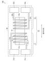
- FIG. 1 is a plan view of a digital isolator according to a first embodiment of the invention.
- FIG. 2 is a plan view of the circuit board of FIG. 1.
- FIG. 3 is a cross-sectional view taken along line AA of the circuit board shown in FIG.
- FIG. 4 is a perspective view showing the circuit board assembly sheet.
- FIG. 5 is a process cross-sectional view for explaining an example of the first method of manufacturing a circuit board.
- FIG. 6 is a process cross-sectional view for explaining an example of the first method of manufacturing a circuit board.
- FIG. 7 is a process cross-sectional view for explaining an example of the first method of manufacturing a circuit board.
- FIG. 8 is a process cross-sectional view for explaining an example of the first method of manufacturing a circuit board.
- FIG. 9 is a process cross-sectional view for explaining an example of the first method for manufacturing a circuit board.
- FIG. 10 is a process cross-sectional view for explaining an example of the first method of manufacturing a circuit board.
- FIG. 11 is a process cross-sectional view for explaining an example of the second manufacturing method of a circuit board.
- FIG. 12 is a process cross-sectional view for explaining an example of the second manufacturing method of a circuit board.
- FIG. 13 is a process cross-sectional view for explaining an example of the second manufacturing method of a circuit board.
- FIG. 14 is a process cross-sectional view for explaining an example of the second manufacturing method of a circuit board.
- FIG. 15 is a process cross-sectional view for explaining an example of the third method of manufacturing a circuit board.
- FIG. 16 is a process cross-sectional view for explaining an example of the third manufacturing method of a circuit board.
- FIG. 17 is a process cross-sectional view for explaining an example of the third method for manufacturing a circuit board.
- FIG. 18 is an enlarged plan view showing a part of the circuit board. It is a figure showing the composition of the circuit board concerning the 2nd embodiment of the present invention. It is a figure showing the composition of the circuit board concerning a 3rd embodiment of the present invention.
- 21 is a process cross-sectional view for explaining an example of a method for manufacturing the circuit board of FIG. 20.
- FIG. 21 is a process cross-sectional view for explaining an example of a method for manufacturing the circuit board of FIG. 20.
- FIG. 21 is a process cross-sectional view for explaining an example of a method for manufacturing the circuit board of FIG. 20.
- FIG. 21 is a process cross-sectional view for explaining an example of a method for manufacturing the circuit board of FIG. 20.
- FIG. 21 is
- FIG. 1 is a plan view of a digital isolator according to a first embodiment of the present invention.
- digital isolator 200 includes a circuit board 100 and a chip package 110. Details of the configuration of the circuit board 100 will be described later.
- Digital isolator 200 may further include an encoder that encodes the electrical signal, a decoder that decodes the electrical signal, or an amplifier that amplifies the electrical signal.
- the chip package 110 is made of ceramic or resin.
- the chip package 110 has, for example, a rectangular parallelepiped shape.
- the width direction the direction along one pair of sides of the chip package 110
- the arrangement direction the direction along the other pair of sides of the chip package 110
- the length of the chip package 110 in the width direction is slightly larger than the length of the circuit board 100 in the longitudinal direction, which will be described later.
- a circuit board 100 is housed within the chip package 110.
- two circuit boards 100 are housed in the chip package 110 so as to be lined up in the arrangement direction, but the number of circuit boards 100 housed in the chip package 110 is not limited.
- the length of the chip package 110 in the arrangement direction is determined according to the number of circuit boards 100 housed inside.
- the chip package 110 may further accommodate an encoder, decoder, amplifier, or the like (not shown).
- a plurality of (four in this example) input terminals 111 to 114 are provided so as to be lined up in the arrangement direction.
- a plurality of (four in this example) output terminals 115 to 118 are provided so as to be lined up in the arrangement direction.
- Input terminals 111 and 112 and output terminals 115 and 116 are connected to one circuit board 100.
- a magnetic field is generated by one of the circuit boards 100.
- an AC electric signal induced by the generated magnetic field is output between the output terminals 115 and 116.
- input terminals 113 and 114 and output terminals 117 and 118 are connected to the other circuit board 100.
- an AC electrical signal is input between the input terminals 113 and 114, a magnetic field is generated by the other circuit board 100. Further, an AC electric signal induced by the generated magnetic field is output between the output terminals 117 and 118.
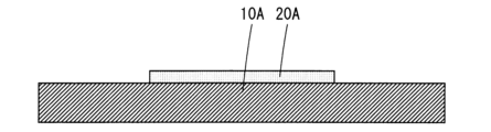
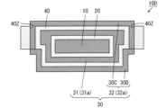
- FIG. 2 is a plan view of the circuit board 100 of FIG. 1.
- FIG. 3 is a cross-sectional view taken along line AA of the circuit board 100 in FIG.
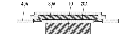
- the circuit board 100 includes a core 10, a base insulating layer 20, a conductor layer 30, and a cover insulating layer 40.
- the internal structure of the cover insulating layer 40 is mainly illustrated, and the illustration of the base insulating layer 20 is omitted.
- the core 10 is formed of a magnetic material.
- the magnetic material includes, for example, SUS430, amorphous, silicon steel, iron, or permalloy.
- Core 10 is preferably formed from a ferromagnetic material such as silicon steel, iron or permalloy.
- the core 10 has a flat plate shape extending in one direction.
- the thickness of the core 10 is, for example, 10 ⁇ m or more and 300 ⁇ m or less.
- the longitudinal direction in which the core 10 extends.
- the base insulating layer 20 is formed of resin such as polyimide. Base insulating layer 20 surrounds core 10 and electrically insulates between core 10 and conductor layer 30 .
- the thickness of the base insulating layer 20 is, for example, 5 ⁇ m or more and 10 ⁇ m or less.
- the conductor layer 30 includes an input conductor layer 31 and an output conductor layer 32 that are electrically insulated from each other. The thickness of the conductor layer 30 is, for example, 5 ⁇ m or more and 30 ⁇ m or less.
- the input conductor layer 31 includes a coil portion 31a, wiring 31b, 31c, and terminals 31d, 31e.
- the coil portion 31a is wound around the core 10 via the base insulating layer 20.
- One end of the coil portion 31a is drawn out from the core 10 and connected to one end of the wiring 31b.
- the other end of the coil portion 31a is drawn out from the core 10 and connected to one end of the wiring 31c.
- the terminals 31d and 31e are arranged at one end of the circuit board 100 in the longitudinal direction.
- the terminal 31d is connected to the other end of the wiring 31b. Further, the terminal 31d is electrically connected to the input terminal 111 or the input terminal 113 in FIG.
- Terminal 31e is connected to the other end of wiring 31c. Further, the terminal 31e is electrically connected to the input terminal 112 or the input terminal 114 in FIG.
- the widths of the terminals 31d and 31e are larger than the widths of the wirings 31b and 31c.
- the output conductor layer 32 includes a coil portion 32a, wiring 32b, 32c, and terminals 32d, 32e.
- the coil portion 32a is arranged to face the coil portion 31a, and is wound around the core 10 via the base insulating layer 20.
- the coil portion 31a and the coil portion 32a are spaced apart from each other by, for example, 10 ⁇ m or more.
- One end of the coil portion 32a is drawn out from the core 10 and connected to one end of the wiring 32b.
- the other end of the coil portion 32a is drawn out from the core 10 and connected to one end of the wiring 32c.
- the terminals 32d and 32e are arranged on the other end side in the longitudinal direction of the circuit board 100.
- the terminal 32d is connected to the other end of the wiring 32b. Further, the terminal 32d is electrically connected to the output terminal 115 or the output terminal 117 in FIG. Terminal 32e is connected to the other end of wiring 32c. Further, the terminal 32e is electrically connected to the output terminal 116 or the output terminal 118 in FIG.
- the widths of the terminals 32d and 32e are larger than the widths of the wirings 32b and 32c.
- the cover insulating layer 40 is formed of resin such as polyimide, and completely covers the conductor layer 30.
- the thickness of the cover insulating layer 40 is, for example, 8 ⁇ m or more and 50 ⁇ m or less.
- the length of the cover insulating layer 40 in the longitudinal direction, that is, the length of the circuit board 100 in the longitudinal direction is, for example, 1630 ⁇ m.
- the circuit board 100 is housed in the chip package 110 with its longitudinal direction facing the width direction of the chip package 110 in FIG.
- FIG. 4 is a perspective view showing a circuit board assembly sheet. As shown in FIG. 4, in this embodiment, a plurality of circuit boards 100 are formed on a circuit board assembly sheet 1 in an aligned state by a roll-to-roll method. Hereinafter, various examples of methods for manufacturing the circuit board 100 will be described with reference to a cross section of one circuit board 100 formed on the circuit board assembly sheet 1.
- 5 to 10 are process cross-sectional views for explaining an example of the first manufacturing method of the circuit board 100.
- 5 to 10 correspond to cross-sectional views taken along the line AA of the circuit board 100 in FIG.
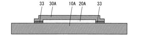
- a sheet 10A made of a magnetic material is prepared, and a base insulating layer 20A is formed in a predetermined region on the upper surface of the sheet 10A.
- the base insulating layer 20A may be formed by applying a photosensitive resin precursor to the upper surface of the sheet 10A and partially exposing the photosensitive resin precursor to ultraviolet light.
- the material of the base insulating layer 20A is polyimide, but it may be other resin such as epoxy.
- a conductor layer 30A is formed on the upper surface of the sheet 10A so as to cover the base insulating layer 20A.
- the conductor layer 30A mainly constitutes parts of the coil parts 31a and 32a, the wirings 31b, 31c, 32b, and 32c, and the terminals 31d, 31e, 32d, and 32e in FIG.
- the conductor layer 30A may be formed by an additive method, a semi-additive method, or another method such as a subtractive method.
- the cross-sectional shape of each part of the conductor layer 30A formed by these manufacturing methods has a quadrilateral shape such as a square, a rectangle, or a trapezoid.
- a seed layer 33 is formed in the boundary area between the conductor layer 30A and the sheet 10A. Therefore, the conductor layer 30A does not come into direct contact with the sheet 10A, but rather through the base insulating layer 20A or the seed layer 33.
- the seed layer 33 includes a material that is resistant to an etching solution to be described later, such as chromium, chromium copper, or nickel chromium.
- a cover insulating layer 40A is formed on the upper surface of the sheet 10A so as to cover the conductor layer 30A.
- the procedure for forming the cover insulating layer 40A is the same as the procedure for forming the base insulating layer 20A.
- a mask (not shown) is formed on the other surface of the sheet 10A so that unnecessary portions of the sheet 10A are exposed, and the portions of the sheet 10A exposed from the mask are etched using an etching solution.
- the core 10 is formed by removing unnecessary portions of the sheet 10A.
- a ferric chloride solution is used as the etching solution. Since the conductor layer 30A is protected by the seed layer 33 that is resistant to etching liquid, the conductor layer 30A remains without being removed in the etching process. That is, the seed layer 33 functions as a barrier layer that protects the conductor layer 30A from the etching solution.
- the seed layer 33 may be removed after the etching process is completed, or may remain. In subsequent steps, illustration of the seed layer 33 is omitted.
- a base insulating layer 20B is formed on the lower surface of the cover insulating layer 40A so as to cover the lower surface of the core 10. A portion of the lower surface of the conductor layer 30A is exposed from the base insulating layer 20B.
- the procedure for forming the base insulating layer 20B is the same as the procedure for forming the base insulating layer 20A.
- the base insulating layer 20 is formed by connecting the base insulating layer 20A and the base insulating layer 20B.
- a conductor layer 30B is formed to cover the base insulating layer 20B on the lower surface of the core 10.
- the procedure for forming the conductor layer 30B is the same as the procedure for forming the conductor layer 30A.
- the conductor layer 30B mainly constitutes another part of the coil parts 31a and 32a in FIG.
- the conductor layer 30 is formed by connecting the conductor layer 30A and the conductor layer 30B.
- a cover insulating layer 40B is formed to cover the conductor layer 30B.
- the procedure for forming the insulating cover layer 40B is the same as the procedure for forming the insulating cover layer 40A.
- the cover insulating layer 40 is formed by connecting the cover insulating layer 40A and the cover insulating layer 40B. In this example, the cover insulating layer 40A and the cover insulating layer 40B are connected via the base insulating layer 20B. As a result, the circuit board 100 is completed.
- FIG. 11 to 14 are process cross-sectional views for explaining an example of the second manufacturing method of the circuit board 100.
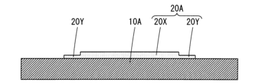
- a sheet 10A made of a magnetic material is prepared, and a base insulating layer 20A is formed in a predetermined region on the upper surface of the sheet 10A.
- the base insulating layer 20A has a thick portion 20X and a thin portion 20Y.
- the thickness of the thin portion 20Y is smaller than the thickness of the thick portion 20X.
- the thin portion 20Y is located in the boundary area between the conductor layer 30A and the sheet 10A, which will be formed in the next step.
- a conductor layer 30A is formed on the base insulating layer 20A.
- the conductor layer 30A does not come into direct contact with the sheet 10A, but comes into contact with the base insulating layer 20A.
- a cover insulating layer 40A is formed on the upper surface of the sheet 10A so as to cover the conductor layer 30A.
- the core 10 is formed by etching the sheet 10A.
- the conductor layer 30A is protected by the thin portion 20Y of the base insulating layer 20A, so the conductor layer 30A remains without being removed in the etching process.
- the thin portion 20Y of the base insulating layer 20A is removed by etching. Thereafter, steps similar to those in FIGS. 9 and 10 are performed to sequentially form the base insulating layer 20B, the conductor layer 30B, and the cover insulating layer 40B. As a result, the circuit board 100 is completed.
- 15 to 17 are process cross-sectional views for explaining an example of the third manufacturing method of the circuit board 100.
- a sheet 10A made of a magnetic material is prepared, and a base insulating layer 20A is formed in a predetermined region on the upper surface of the sheet 10A.
- the formation area of the base insulating layer 20A in this example is larger than the formation area of the base insulating layer 20A in FIG. 5 in the first manufacturing method.
- Two openings 20Z are formed in the base insulating layer 20A. Each opening 20Z is used as a via hole.
- a seed layer 33 is formed on the upper surface of the sheet 10A exposed within each opening 20Z of the base insulating layer 20A. Further, a conductor layer 30A is formed on a predetermined region of the base insulating layer 20A. A portion of the conductor layer 30A is formed within the opening 20Z. Therefore, the conductor layer 30A does not come into direct contact with the sheet 10A, but rather through the base insulating layer 20A or the seed layer 33.
- a cover insulating layer 40A is formed on the base insulating layer 20A so as to cover the conductor layer 30A.
- the sheet 10A is etched by performing steps similar to those in FIGS. 8 to 10, and the base insulating layer 20B, the conductor layer 30B, and the cover insulating layer 40B are sequentially formed.
- a circuit board 100 similar to the circuit board 100 of FIG. 10 is completed, except that a portion of the cover insulating layer 40A is formed by the base insulating layer 20A.
- the coil portion 31a and the coil portion 32a are magnetically coupled, and electrical signals or power are transmitted while being electrically insulated from each other.
- the coil parts 31a and 32a are wound around a thin and common core 10 made of a magnetic material, a large magnetic coupling occurs between the coil parts 31a and 32a. Therefore, when the circuit board 100 is used as a digital isolator or a transformer, generation of large noise in the surroundings is prevented.
- the core 10 is formed of a ferromagnetic material such as silicon steel, iron, or permalloy, the magnetic coupling between the coil parts 31a and 32a can be further increased.
- the magnetic coupling between the coil parts 31a and 32a is large, it becomes possible to arrange the coil part 31a and the coil part 32a apart from each other. This maintains the dielectric strength between the coil parts 31a and 32a. Further, since only the end surfaces of the coil portion 31a and the coil portion 32a face each other, the opposing area between the coil portion 31a and the coil portion 32a is small. Therefore, the parasitic capacitance generated between the coil portion 31a and the coil portion 32a is small. In this case, it is possible to transmit high frequency electrical signals or power with low delay. As a result, it is possible to downsize the circuit board 100 while configuring the circuit board 100 as a magnetic component.
- the conductor layer 30 can be formed using a wiring circuit board forming technique such as an additive method, a semi-additive method, or a subtractive method. Therefore, the circuit board 100 can be easily formed.
- the coil portion 31a and the coil portion 32a are spaced apart by, for example, 10 ⁇ m or more. That is, the shortest distance between the coil portion 31a and the coil portion 32a is, for example, 10 ⁇ m. In this case, the dielectric strength between the coil portion 31a and the coil portion 32a can be sufficiently maintained.
- the cover insulating layer 40 (cover insulating layer 40A) is formed on the upper surface of the region of the circuit board assembly sheet 1 that will be removed by etching. (See Figure 7). According to this configuration, even if a part of the circuit board assembly sheet 1 is removed by etching, the cover insulating layer 40A remains, so that in the step of forming the base insulating layer 20B, the base insulating layer 20B is removed from the circuit board. It is not formed by wrapping around the upper surface of the aggregate sheet 1 (see FIG. 9). This prevents the yield from decreasing.
- the cover insulating layer 40 is also formed on the conductor layer 30, the conductor layer 30 is prevented from corroding even when the circuit board 100 is used for a long period of time. Thereby, the life of the circuit board 100 can be extended.
- FIG. 18 is an enlarged plan view showing a part of the circuit board 100.
- the left side of FIG. 18 shows the circuit board 100 manufactured by the third manufacturing method of the circuit board 100.
- the width of the wiring portion of the coil parts 31a and 32a exposed from the opening 20Z is equal to the width of the opening. It is slightly larger than the diameter of the portion 20Z. Therefore, in order to prevent interference between the conductor layers 30A, it is necessary to increase the width between the wires in the coil portions 31a and 32a.
- the right side of FIG. 18 shows the circuit board 100 manufactured by the first or second manufacturing method of the circuit board 100.
- conductor layer 30A and conductor layer 30B are electrically connected without via holes.
- the width of the wiring portion in the coil portions 31a and 32a can be reduced overall. Therefore, there is no need to increase the width between the wires in the coil parts 31a, 32a, and the coil parts 31a, 32a can be wound tightly. Thereby, the circuit board 100 can be made smaller.
- FIG. 19 is a diagram showing the configuration of a circuit board 100 according to the second embodiment of the present invention.
- FIG. 19 A perspective view of the circuit board 100 is shown on the left side of FIG. 19, and an enlarged cross section of the circuit board 100 is shown on the right side.
- FIG. 19 illustrations of the terminals 31d, 31e, 32d, and 32e in FIG. 2, and the base insulating layer 20 and cover insulating layer 40 in FIG. 3 are omitted. Note that the positions of the terminals 31d, 31e, 32d, and 32e are not limited to the example in FIG. 2.
- a hatching pattern is added to the output conductor layer 32 in order to easily identify the input conductor layer 31 and the output conductor layer 32. The same applies to FIG. 20, which will be described later.
- the coil portion 31a and the coil portion 32a are wound around the core 10 such that the wiring of the coil portion 31a and the wiring of the coil portion 32a are arranged alternately in the longitudinal direction. be done.
- the method for manufacturing circuit board 100 according to this embodiment is similar to the method for manufacturing circuit board 100 according to the first embodiment. Therefore, the circuit board 100 according to the present embodiment may be manufactured using any of the first to third manufacturing methods.
- the coil portion 31a and the coil portion 32a are closer to each other than in the circuit board 100 according to the first embodiment. Therefore, magnetic coupling between the coil portion 31a and the coil portion 32a increases, thereby reducing leakage magnetic flux. This allows electrical signals or power to be transmitted with higher efficiency.
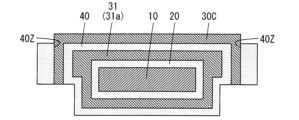
- FIG. 20 is a diagram showing the configuration of a circuit board 100 according to the third embodiment of the present invention. As shown in FIG. 20, in this embodiment, coil portion 31a and coil portion 32a are wound around core 10 so as to be concentrically stacked.
- 21 to 24 are process cross-sectional views for explaining an example of a method for manufacturing the circuit board 100 of FIG. 20.
- the circuit board shown in FIG. 21 is manufactured by executing the manufacturing method shown in FIGS. 5 to 10.
- the circuit board in FIG. 21 has the same configuration as the circuit board 100 in FIG. 10 except that only the input conductor layer 31 is formed as the conductor layer 30 and the output conductor layer 32 is not formed. In FIG. 21, only the coil portion 31a of the input conductor layer 31 appears.
- a plurality of openings 40Z penetrating the cover insulating layer 40 are formed. Approximately half of the openings 40Z among the plurality of openings 40Z are arranged on one side of the coil portion 31a so as to be lined up in the longitudinal direction. Approximately half of the remaining openings 40Z among the plurality of openings 40Z are arranged on the other side of the coil portion 31a so as to be lined up in the longitudinal direction.
- a conductor layer 30C is formed on a predetermined region of the upper surface of the cover insulating layer 40 and in each opening 40Z.
- the procedure for forming the conductor layer 30C is the same as the procedure for forming the conductor layers 30A and 30B.
- the conductor layer 30C mainly constitutes a part of the coil portion 32a in FIG. 20, the wirings 32b and 32c, and the terminals 32d and 32e in FIG.
- a conductor layer 30D is formed in a predetermined region on the lower surface of the cover insulating layer 40.
- the procedure for forming conductor layer 30D is the same as the procedure for forming conductor layers 30A to 30C.
- the conductor layer 30D mainly constitutes another part of the coil portion 32a in FIG. 20.
- the output conductor layer 32 is formed by connecting the conductor layer 30C and the conductor layer 30D through the opening 40Z. In FIG. 24, only the coil portion 32a of the output conductor layer 32 is visible.
- the coil portion 32a is wound around the coil portion 31a via the cover insulating layer 40.
- a cover insulating layer may be further formed on the upper and lower surfaces of the cover insulating layer 40 so as to cover the output conductor layer 32 .
- the coil part 31a and the coil part 32a are closer to each other than in the circuit board 100 according to the second embodiment. Therefore, the magnetic coupling between the coil portion 31a and the coil portion 32a further increases, thereby further reducing the leakage magnetic flux. This allows electrical signals or power to be transmitted with even higher efficiency.
- the wirings 31b, 31c, 32b, 32c and the terminals 31d, 31e, 32d, 32e are constituted by the conductor layer 30A, but the embodiments are not limited thereto.
- the wirings 31b, 31c, 32b, 32c and the terminals 31d, 31e, 32d, 32e may be formed of the conductor layer 30B.
- some of the wirings 31b, 31c, 32b, 32c and the terminals 31d, 31e, 32d, 32e may be formed by the conductor layer 30A, and the other portions may be formed by the conductor layer 30B.
- each part of the conductor layer 30 has a quadrangular cross-sectional shape, but the embodiment is not limited to this.
- the cross-sectional shape of each part of the conductor layer 30 may have a shape different from a square, for example, a circular shape.
- the conductor layer 30 includes a coil portion 31a, wirings 31b, 31c, and terminals 31d, 31e, and a coil portion 32a, wirings 32b, 32c, and terminals 32d, 32e.
- the conductor layer 30 does not need to include one of the coil portion 31a, the wires 31b, 31c, and the terminals 31d, 31e, and the coil portion 32a, the wires 32b, 32c, and the terminals 32d, 32e.
- This circuit board manufacturing method includes preparing a core made of a magnetic material and having a thickness of 10 ⁇ m or more and 300 ⁇ m or less, forming an insulating layer around the core, and forming a conductive layer.
- the conductor layer may include a coil wound around the core via the insulating layer, and first wiring and second wiring connected to the coil.
- the core 10 is an example of the core
- the base insulating layer 20 is an example of an insulating layer
- the coil parts 31a and 32a are examples of first and second coils, respectively.
- the wirings 31b and 31c are examples of first and second wirings, respectively
- the wirings 32b and 32c are examples of third and fourth wirings, respectively
- the circuit board 100 is an example of a circuit board
- the digital isolator 200 is an example of a circuit board. is an example of a digital isolator.
- the base insulating layer 20 and the cover insulating layer 40 are examples of the first and second insulating layers
- the conductor layer 30 is an example of the conductor layer
- the base insulating layers 20A and 20B are the first and second parts, respectively. This is an example.
- the conductor layers 30A and 30B are examples of the third and fourth portions
- the circuit board assembly sheet 1 is an example of a sheet
- the seed layer 33 is an example of a seed layer
- the thick portion 20X is an example of a thick portion. This is an example of a thin wall portion
- the thin wall portion 20Y is an example of a thin wall portion.
Landscapes
- Engineering & Computer Science (AREA)
- Power Engineering (AREA)
- Microelectronics & Electronic Packaging (AREA)
- Coils Or Transformers For Communication (AREA)
- Parts Printed On Printed Circuit Boards (AREA)
Abstract
Cette carte de circuit imprimé comprend un noyau, une couche d'isolation de base, une première et une seconde partie de bobine, et des premier à quatrième câblages. Le noyau est constitué d'un matériau magnétique et a une épaisseur de 10 µm à 300 µm. La couche d'isolation de base est disposée autour du noyau. La première partie de bobine et la seconde partie de bobine sont enroulées autour du noyau avec la couche d'isolation de base entre celles-ci. Le premier câblage et le deuxième câblage sont connectés à la première partie de bobine. Le troisième câblage et le quatrième câblage sont connectés à la seconde partie de bobine.
Priority Applications (1)
| Application Number | Priority Date | Filing Date | Title |
|---|---|---|---|
| JP2024517955A JPWO2023210317A1 (fr) | 2022-04-28 | 2023-04-10 |
Applications Claiming Priority (2)
| Application Number | Priority Date | Filing Date | Title |
|---|---|---|---|
| JP2022075049 | 2022-04-28 | ||
| JP2022-075049 | 2022-04-28 |
Publications (1)
| Publication Number | Publication Date |
|---|---|
| WO2023210317A1 true WO2023210317A1 (fr) | 2023-11-02 |
Family
ID=88518377
Family Applications (1)
| Application Number | Title | Priority Date | Filing Date |
|---|---|---|---|
| PCT/JP2023/014499 Ceased WO2023210317A1 (fr) | 2022-04-28 | 2023-04-10 | Carte de circuit imprimé, isolateur numérique ou transformateur, et procédé de fabrication de carte de circuit imprimé |
Country Status (2)
| Country | Link |
|---|---|
| JP (1) | JPWO2023210317A1 (fr) |
| WO (1) | WO2023210317A1 (fr) |
Citations (5)
| Publication number | Priority date | Publication date | Assignee | Title |
|---|---|---|---|---|
| JPH10154795A (ja) * | 1996-11-19 | 1998-06-09 | Advanced Materials Eng Res Inc | 半導体チップにおけるインダクター及びその製造方法 |
| JP2005223129A (ja) * | 2004-02-05 | 2005-08-18 | Rohm Co Ltd | コイル装置 |
| JP2013527620A (ja) * | 2010-05-26 | 2013-06-27 | タイコ・エレクトロニクス・コーポレイション | 平面インダクタデバイス |
| JP2017028064A (ja) * | 2015-07-21 | 2017-02-02 | 太陽誘電株式会社 | モジュール基板 |
| JP2018046181A (ja) * | 2016-09-15 | 2018-03-22 | 大日本印刷株式会社 | インダクタおよびインダクタの製造方法 |
-
2023
- 2023-04-10 WO PCT/JP2023/014499 patent/WO2023210317A1/fr not_active Ceased
- 2023-04-10 JP JP2024517955A patent/JPWO2023210317A1/ja active Pending
Patent Citations (5)
| Publication number | Priority date | Publication date | Assignee | Title |
|---|---|---|---|---|
| JPH10154795A (ja) * | 1996-11-19 | 1998-06-09 | Advanced Materials Eng Res Inc | 半導体チップにおけるインダクター及びその製造方法 |
| JP2005223129A (ja) * | 2004-02-05 | 2005-08-18 | Rohm Co Ltd | コイル装置 |
| JP2013527620A (ja) * | 2010-05-26 | 2013-06-27 | タイコ・エレクトロニクス・コーポレイション | 平面インダクタデバイス |
| JP2017028064A (ja) * | 2015-07-21 | 2017-02-02 | 太陽誘電株式会社 | モジュール基板 |
| JP2018046181A (ja) * | 2016-09-15 | 2018-03-22 | 大日本印刷株式会社 | インダクタおよびインダクタの製造方法 |
Also Published As
| Publication number | Publication date |
|---|---|
| JPWO2023210317A1 (fr) | 2023-11-02 |
Similar Documents
| Publication | Publication Date | Title |
|---|---|---|
| CN100389521C (zh) | 方向性耦合器 | |
| US7508292B2 (en) | Coil component | |
| US20140049353A1 (en) | Inductor and method of manufacturing inductor | |
| JP2005317724A (ja) | コイル部品 | |
| KR20130072816A (ko) | 인덕터의 제조 방법 | |
| JP2023062846A (ja) | コイル部品及びその製造方法 | |
| CN110415945A (zh) | 变压器及其制作方法和电磁器件 | |
| KR20230126921A (ko) | 평면 변압기 및 그 제조 방법 | |
| CN110415944B (zh) | 变压器及其制作方法和电磁器件 | |
| JP2008109139A (ja) | いくつかのコイルブランチを有するコイル、及び当該コイルの一つを有するマイクロインダクタ | |
| WO2023210317A1 (fr) | Carte de circuit imprimé, isolateur numérique ou transformateur, et procédé de fabrication de carte de circuit imprimé | |
| CN110415940B (zh) | 集成变压器及电子装置 | |
| JP2010118367A (ja) | 分配器 | |
| JP2017199718A (ja) | 電子部品およびその製造方法 | |
| JP2021132074A (ja) | コイル部品及びこれを備える回路基板 | |
| WO2023149352A1 (fr) | Bobine, composant inducteur et réseau d'inducteurs | |
| WO2023210247A1 (fr) | Carte de circuit imprimé de câblage et procédé de production d'un circuit imprimé de câblage | |
| JP2002359115A (ja) | チップ型コモンモードチョークコイル | |
| CN100530816C (zh) | 方向性耦合器 | |
| JP2008053754A (ja) | コイル部品 | |
| TWI885676B (zh) | 具內埋電感的電路板及其製造方法 | |
| CN110415946B (zh) | 电磁元件及其制造方法 | |
| TWI530968B (zh) | Magnetic coil structure | |
| CN111799077A (zh) | 变压器、变压器的制作方法和电磁器件 | |
| WO2011118072A1 (fr) | Carte de circuit imprimé |
Legal Events
| Date | Code | Title | Description |
|---|---|---|---|
| 121 | Ep: the epo has been informed by wipo that ep was designated in this application |
Ref document number: 23796063 Country of ref document: EP Kind code of ref document: A1 |
|
| ENP | Entry into the national phase |
Ref document number: 2024517955 Country of ref document: JP Kind code of ref document: A |
|
| NENP | Non-entry into the national phase |
Ref country code: DE |
|
| 122 | Ep: pct application non-entry in european phase |
Ref document number: 23796063 Country of ref document: EP Kind code of ref document: A1 |