WO2023210399A1 - Plasma treatment device, power source system, and plasma treatment method - Google Patents
Plasma treatment device, power source system, and plasma treatment method Download PDFInfo
- Publication number
- WO2023210399A1 WO2023210399A1 PCT/JP2023/015084 JP2023015084W WO2023210399A1 WO 2023210399 A1 WO2023210399 A1 WO 2023210399A1 JP 2023015084 W JP2023015084 W JP 2023015084W WO 2023210399 A1 WO2023210399 A1 WO 2023210399A1
- Authority
- WO
- WIPO (PCT)
- Prior art keywords
- power
- supply
- time
- peak
- level
- Prior art date
- Legal status (The legal status is an assumption and is not a legal conclusion. Google has not performed a legal analysis and makes no representation as to the accuracy of the status listed.)
- Ceased
Links
Images


Classifications
-
- H—ELECTRICITY
- H01—ELECTRIC ELEMENTS
- H01J—ELECTRIC DISCHARGE TUBES OR DISCHARGE LAMPS
- H01J37/00—Discharge tubes with provision for introducing objects or material to be exposed to the discharge, e.g. for the purpose of examination or processing thereof
- H01J37/32—Gas-filled discharge tubes
- H01J37/32009—Arrangements for generation of plasma specially adapted for examination or treatment of objects, e.g. plasma sources
- H01J37/32082—Radio frequency generated discharge
- H01J37/32091—Radio frequency generated discharge the radio frequency energy being capacitively coupled to the plasma
-
- H—ELECTRICITY
- H01—ELECTRIC ELEMENTS
- H01J—ELECTRIC DISCHARGE TUBES OR DISCHARGE LAMPS
- H01J37/00—Discharge tubes with provision for introducing objects or material to be exposed to the discharge, e.g. for the purpose of examination or processing thereof
- H01J37/32—Gas-filled discharge tubes
- H01J37/32009—Arrangements for generation of plasma specially adapted for examination or treatment of objects, e.g. plasma sources
- H01J37/32082—Radio frequency generated discharge
- H01J37/32137—Radio frequency generated discharge controlling of the discharge by modulation of energy
- H01J37/32146—Amplitude modulation, includes pulsing
-
- C—CHEMISTRY; METALLURGY
- C23—COATING METALLIC MATERIAL; COATING MATERIAL WITH METALLIC MATERIAL; CHEMICAL SURFACE TREATMENT; DIFFUSION TREATMENT OF METALLIC MATERIAL; COATING BY VACUUM EVAPORATION, BY SPUTTERING, BY ION IMPLANTATION OR BY CHEMICAL VAPOUR DEPOSITION, IN GENERAL; INHIBITING CORROSION OF METALLIC MATERIAL OR INCRUSTATION IN GENERAL
- C23C—COATING METALLIC MATERIAL; COATING MATERIAL WITH METALLIC MATERIAL; SURFACE TREATMENT OF METALLIC MATERIAL BY DIFFUSION INTO THE SURFACE, BY CHEMICAL CONVERSION OR SUBSTITUTION; COATING BY VACUUM EVAPORATION, BY SPUTTERING, BY ION IMPLANTATION OR BY CHEMICAL VAPOUR DEPOSITION, IN GENERAL
- C23C16/00—Chemical coating by decomposition of gaseous compounds, without leaving reaction products of surface material in the coating, i.e. chemical vapour deposition [CVD] processes
- C23C16/44—Chemical coating by decomposition of gaseous compounds, without leaving reaction products of surface material in the coating, i.e. chemical vapour deposition [CVD] processes characterised by the method of coating
- C23C16/50—Chemical coating by decomposition of gaseous compounds, without leaving reaction products of surface material in the coating, i.e. chemical vapour deposition [CVD] processes characterised by the method of coating using electric discharges
- C23C16/505—Chemical coating by decomposition of gaseous compounds, without leaving reaction products of surface material in the coating, i.e. chemical vapour deposition [CVD] processes characterised by the method of coating using electric discharges using radio frequency discharges
- C23C16/509—Chemical coating by decomposition of gaseous compounds, without leaving reaction products of surface material in the coating, i.e. chemical vapour deposition [CVD] processes characterised by the method of coating using electric discharges using radio frequency discharges using internal electrodes
-
- H—ELECTRICITY
- H01—ELECTRIC ELEMENTS
- H01J—ELECTRIC DISCHARGE TUBES OR DISCHARGE LAMPS
- H01J37/00—Discharge tubes with provision for introducing objects or material to be exposed to the discharge, e.g. for the purpose of examination or processing thereof
- H01J37/32—Gas-filled discharge tubes
- H01J37/32009—Arrangements for generation of plasma specially adapted for examination or treatment of objects, e.g. plasma sources
- H01J37/32082—Radio frequency generated discharge
- H01J37/32174—Circuits specially adapted for controlling the RF discharge
- H01J37/32183—Matching circuits
-
- H—ELECTRICITY
- H01—ELECTRIC ELEMENTS
- H01J—ELECTRIC DISCHARGE TUBES OR DISCHARGE LAMPS
- H01J37/00—Discharge tubes with provision for introducing objects or material to be exposed to the discharge, e.g. for the purpose of examination or processing thereof
- H01J37/32—Gas-filled discharge tubes
- H01J37/32431—Constructional details of the reactor
- H01J37/32715—Workpiece holder
-
- H—ELECTRICITY
- H05—ELECTRIC TECHNIQUES NOT OTHERWISE PROVIDED FOR
- H05H—PLASMA TECHNIQUE; PRODUCTION OF ACCELERATED ELECTRICALLY-CHARGED PARTICLES OR OF NEUTRONS; PRODUCTION OR ACCELERATION OF NEUTRAL MOLECULAR OR ATOMIC BEAMS
- H05H1/00—Generating plasma; Handling plasma
- H05H1/24—Generating plasma
- H05H1/46—Generating plasma using applied electromagnetic fields, e.g. high frequency or microwave energy
-
- H—ELECTRICITY
- H10—SEMICONDUCTOR DEVICES; ELECTRIC SOLID-STATE DEVICES NOT OTHERWISE PROVIDED FOR
- H10P—GENERIC PROCESSES OR APPARATUS FOR THE MANUFACTURE OR TREATMENT OF DEVICES COVERED BY CLASS H10
- H10P14/00—Formation of materials, e.g. in the shape of layers or pillars
- H10P14/20—Formation of materials, e.g. in the shape of layers or pillars of semiconductor materials
- H10P14/29—Formation of materials, e.g. in the shape of layers or pillars of semiconductor materials characterised by the substrates
-
- H—ELECTRICITY
- H10—SEMICONDUCTOR DEVICES; ELECTRIC SOLID-STATE DEVICES NOT OTHERWISE PROVIDED FOR
- H10P—GENERIC PROCESSES OR APPARATUS FOR THE MANUFACTURE OR TREATMENT OF DEVICES COVERED BY CLASS H10
- H10P14/00—Formation of materials, e.g. in the shape of layers or pillars
- H10P14/60—Formation of materials, e.g. in the shape of layers or pillars of insulating materials
-
- H—ELECTRICITY
- H10—SEMICONDUCTOR DEVICES; ELECTRIC SOLID-STATE DEVICES NOT OTHERWISE PROVIDED FOR
- H10P—GENERIC PROCESSES OR APPARATUS FOR THE MANUFACTURE OR TREATMENT OF DEVICES COVERED BY CLASS H10
- H10P50/00—Etching of wafers, substrates or parts of devices
- H10P50/20—Dry etching; Plasma etching; Reactive-ion etching
- H10P50/24—Dry etching; Plasma etching; Reactive-ion etching of semiconductor materials
- H10P50/242—Dry etching; Plasma etching; Reactive-ion etching of semiconductor materials of Group IV materials
-
- H—ELECTRICITY
- H01—ELECTRIC ELEMENTS
- H01J—ELECTRIC DISCHARGE TUBES OR DISCHARGE LAMPS
- H01J2237/00—Discharge tubes exposing object to beam, e.g. for analysis treatment, etching, imaging
- H01J2237/32—Processing objects by plasma generation
- H01J2237/33—Processing objects by plasma generation characterised by the type of processing
- H01J2237/332—Coating
- H01J2237/3321—CVD [Chemical Vapor Deposition]
Definitions
- the present disclosure relates to a plasma processing apparatus, a power supply system, and a plasma processing method.
- Patent Document 1 provides a method of etching a SiOC-based low-k film or the like using a SiC film as a base film.
- the power of the RF power source is slowed up to a second power value and then placed in a power modulation mode.
- the DC voltage of the variable DC power supply is slowed down. By slowing down either of these, damage to the wafer or power supply can be reduced.
- the present disclosure provides a technique that can suppress plasma load fluctuations.
- a plasma processing chamber a substrate support section provided in the plasma processing chamber and on which a substrate is placed, a gas supply section supplying a processing gas to the plasma processing chamber, and the an RF power source that supplies pulsed RF power to the plasma processing chamber and/or the substrate support to generate plasma of the processing gas; and a control device that controls the supply of the pulsed RF power.
- control device is configured such that an increasing function of the power level from the start point of supply of the pulsed RF power to the point of peak occurrence is a downwardly convex function, and/or the control device
- a plasma processing apparatus is provided in which the RF power source is controlled so that a decreasing function of the power level from a peak end point to a supply end point is a downwardly convex function.
- plasma load fluctuations can be suppressed.
- FIG. 1 is a diagram showing an example of a plasma processing apparatus according to an embodiment. The figure which shows the transition sequence example of the continuous wave of RF electric power, and a pulse wave of a reference example.
- FIG. 3 is a diagram showing an example of a transition sequence between a continuous wave and a pulse wave of RF power according to the embodiment.
- FIG. 7 is a diagram showing an increasing function of the power level of an RF pulse in a reference example during a ramp-up period.
- FIG. 4 is a diagram illustrating an increasing function of the power level of the RF pulse for an embodiment of the ramp-up period.
- FIG. 6 is a diagram illustrating a decreasing function of the power level of an RF pulse for an embodiment of a ramp-down period.
- 1 is a flowchart illustrating an example of a plasma processing method according to an embodiment.
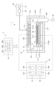
- FIG. 1 is a diagram for explaining a configuration example of a capacitively coupled plasma processing apparatus.
- the plasma processing apparatus 1 is a capacitively coupled plasma processing apparatus, and includes a plasma processing chamber 10, a gas supply section 20, a power supply 30, an exhaust system 40, and a control device 2. Further, the plasma processing apparatus 1 includes a substrate support section 11 and a gas introduction section. The gas inlet is configured to introduce at least one processing gas into the plasma processing chamber 10 .
- the gas introduction section includes a shower head 13.
- Substrate support 11 is arranged within plasma processing chamber 10 .
- the shower head 13 is arranged above the substrate support section 11 . In one embodiment, showerhead 13 forms at least a portion of the ceiling of plasma processing chamber 10 .
- the plasma processing chamber 10 has a plasma processing space 10s defined by a shower head 13, a side wall 10a of the plasma processing chamber 10, and a substrate support 11.
- the plasma processing chamber 10 has at least one gas supply port for supplying at least one processing gas to the plasma processing space 10s, and at least one gas exhaust port for discharging gas from the plasma processing space.
- Plasma processing chamber 10 is grounded.
- the shower head 13 and substrate support 11 are electrically insulated from the casing of the plasma processing chamber 10.
- the substrate support section 11 includes a main body section 111 and a ring assembly 112.
- the main body portion 111 has a central region 111a for supporting the substrate W and an annular region 111b for supporting the ring assembly 112.
- a wafer is an example of a substrate W.
- the annular region 111b of the main body 111 surrounds the central region 111a of the main body 111 in plan view.
- the substrate W is placed on the central region 111a of the main body 111, and the ring assembly 112 is placed on the annular region 111b of the main body 111 so as to surround the substrate W on the central region 111a of the main body 111. Therefore, the central region 111a is also called a substrate support surface for supporting the substrate W, and the annular region 111b is also called a ring support surface for supporting the ring assembly 112.
- the main body 111 includes a base 1110 and an electrostatic chuck 1111.
- Base 1110 includes a conductive member.
- the conductive member of the base 1110 can function as a bottom electrode.
- Electrostatic chuck 1111 is placed on base 1110.
- Electrostatic chuck 1111 includes a ceramic member 1111a and an electrostatic electrode 1111b disposed within ceramic member 1111a.
- Ceramic member 1111a has a central region 111a. In one embodiment, ceramic member 1111a also has an annular region 111b. Note that another member surrounding the electrostatic chuck 1111, such as an annular electrostatic chuck or an annular insulating member, may have the annular region 111b.
- ring assembly 112 may be placed on the annular electrostatic chuck or the annular insulation member, or may be placed on both the electrostatic chuck 1111 and the annular insulation member.
- at least one RF/DC electrode coupled to an RF (Radio Frequency) power source 31 and/or a DC (Direct Current) power source 32, which will be described later, may be disposed within the ceramic member 1111a.
- at least one RF/DC electrode functions as a bottom electrode.
- An RF/DC electrode is also referred to as a bias electrode if a bias RF signal and/or a DC signal, as described below, is supplied to at least one RF/DC electrode.
- the conductive member of the base 1110 and at least one RF/DC electrode may function as a plurality of lower electrodes.
- the electrostatic electrode 1111b may function as a lower electrode. Therefore, the substrate support 11 includes at least one lower electrode.
- Ring assembly 112 includes one or more annular members.
- the one or more annular members include one or more edge rings and at least one cover ring.
- the edge ring is made of a conductive or insulating material
- the cover ring is made of an insulating material.
- the substrate support unit 11 may include a temperature control module configured to adjust at least one of the electrostatic chuck 1111, the ring assembly 112, and the substrate to a target temperature.
- the temperature control module may include a heater, a heat transfer medium, a flow path 1110a, or a combination thereof.
- a heat transfer fluid such as brine or gas flows through the flow path 1110a.
- a channel 1110a is formed within the base 1110 and one or more heaters are disposed within the ceramic member 1111a of the electrostatic chuck 1111.
- the substrate support section 11 may include a heat transfer gas supply section configured to supply heat transfer gas to the gap between the back surface of the substrate W and the central region 111a.
- the shower head 13 is configured to introduce at least one processing gas from the gas supply section 20 into the plasma processing space 10s.
- the shower head 13 has at least one gas supply port 13a, at least one gas diffusion chamber 13b, and a plurality of gas introduction ports 13c.
- the processing gas supplied to the gas supply port 13a passes through the gas diffusion chamber 13b and is introduced into the plasma processing space 10s from the plurality of gas introduction ports 13c.
- the showerhead 13 also includes at least one upper electrode.
- the gas introduction section may include one or more side gas injectors (SGI) attached to one or more openings formed in the side wall 10a.
- SGI side gas injectors
- the gas supply section 20 may include at least one gas source 21 and at least one flow rate controller 22.
- the gas supply 20 is configured to supply at least one process gas from a respective gas source 21 to the showerhead 13 via a respective flow controller 22 .
- Each flow controller 22 may include, for example, a mass flow controller or a pressure-controlled flow controller.
- gas supply 20 may include one or more flow modulation devices that modulate or pulse the flow rate of at least one process gas.
- Power supply 30 includes an RF power supply 31 coupled to plasma processing chamber 10 via at least one impedance matching circuit.
- RF power source 31 is configured to supply at least one RF signal (RF power) to at least one bottom electrode and/or at least one top electrode.
- RF power source 31 may function as at least part of a plasma generation unit configured to generate a plasma from one or more process gases in plasma processing chamber 10 .
- a bias potential is generated in the substrate W, and ion components in the formed plasma can be drawn into the substrate W.
- the RF power supply 31 includes a first RF generation section 31a and a second RF generation section 31b.
- the first RF generation section 31a is coupled to at least one lower electrode and/or at least one upper electrode via at least one impedance matching circuit, and generates a source RF signal (source RF power) for plasma generation. It is configured as follows.
- the source RF signal has a frequency within the range of 10 MHz to 150 MHz.
- the first RF generator 31a may be configured to generate multiple source RF signals having different frequencies. The generated one or more source RF signals are provided to at least one bottom electrode and/or at least one top electrode.
- the second RF generating section 31b is coupled to at least one lower electrode via at least one impedance matching circuit, and is configured to generate a bias RF signal (bias RF power).
- the frequency of the bias RF signal may be the same or different than the frequency of the source RF signal.
- the bias RF signal has a lower frequency than the frequency of the source RF signal.
- the bias RF signal has a frequency within the range of 100kHz to 60MHz.
- the second RF generator 31b may be configured to generate multiple bias RF signals having different frequencies.
- the generated one or more bias RF signals are provided to at least one bottom electrode. Also, in various embodiments, at least one of the source RF signal and the bias RF signal may be pulsed.
- Power source 30 may also include a DC power source 32 coupled to plasma processing chamber 10 .
- the DC power supply 32 includes a first DC generation section 32a and a second DC generation section 32b.
- the first DC generator 32a is connected to at least one lower electrode and configured to generate a first DC signal.
- the generated first bias DC signal is applied to the at least one bottom electrode.
- the second DC generator 32b is connected to the at least one upper electrode and configured to generate a second DC signal.
- the generated second DC signal is applied to the at least one top electrode.
- At least one of the first and second DC signals may be pulsed.
- a sequence of voltage pulses is applied to at least one lower electrode and/or at least one upper electrode.
- the voltage pulse may have a pulse waveform that is rectangular, trapezoidal, triangular, or a combination thereof.
- a waveform generator for generating a sequence of voltage pulses from a DC signal is connected between the first DC generator 32a and the at least one bottom electrode. Therefore, the first DC generation section 32a and the waveform generation section constitute a voltage pulse generation section.
- the voltage pulse generation section is connected to at least one upper electrode.
- the voltage pulse may have positive polarity or negative polarity.
- the sequence of voltage pulses may include one or more positive voltage pulses and one or more negative voltage pulses within one period.
- the first and second DC generation units 32a and 32b may be provided in addition to the RF power source 31, or the first DC generation unit 32a may be provided in place of the second RF generation unit 31b. good.
- the exhaust system 40 may be connected to a gas exhaust port 10e provided at the bottom of the plasma processing chamber 10, for example.
- Evacuation system 40 may include a pressure regulating valve and a vacuum pump. The pressure within the plasma processing space 10s is adjusted by the pressure regulating valve.
- the vacuum pump may include a turbomolecular pump, a dry pump, or a combination thereof.
- the controller 2 processes computer-executable instructions that cause the plasma processing apparatus 1 to perform various steps described in this disclosure.
- Controller 2 may be configured to control each element of plasma processing apparatus 1 to perform the various steps described herein.
- the control device 2 may control the supply of RF power when changing from continuous waves to pulsed waves and from pulsed waves to continuous waves.
- part or all of the control device 2 may be included in the plasma processing apparatus 1.
- the control device 2 may include a processing section 2a1, a storage section 2a2, and a communication interface 2a3.
- the control device 2 is realized by, for example, a computer 2a.
- the processing unit two a1 may be configured to read a program from the storage unit two a2 and perform various control operations by executing the read program.
- This program may be stored in the storage unit 2a2 in advance, or may be acquired via a medium when necessary.
- the acquired program is stored in the storage unit 2a2, and is read out from the storage unit 2a2 and executed by the processing unit 2a1.
- the medium may be various storage media readable by the computer 2a, or may be a communication line connected to the communication interface 2a3.
- the processing unit 2a1 may be a CPU (Central Processing Unit).
- the storage unit 2a2 includes a RAM (Random Access Memory), a ROM (Read Only Memory), an HDD (Hard Disk Drive), an SSD (Solid State Drive), or a combination thereof. You can.
- the communication interface 2a3 may communicate with the plasma processing apparatus 1 via a communication line such as a LAN (Local Area Network).
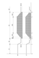
- FIG. 2 is a diagram showing an example of a transition sequence between a continuous wave and a pulse wave of RF power according to a reference example.
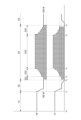
- FIG. 3 is a diagram illustrating an example of a transition sequence between a continuous wave and a pulse wave of RF power according to the embodiment. Note that FIGS. 2 and 3 only show the control conditions for the RF power, and do not show the control conditions for the processing gas, the pressure in the chamber, etc., but from time t 0 to time t in FIGS. 2 and 3 6 and the period after time t6 , plasma processing of the substrate W is performed according to the control conditions set in the recipe used for substrate processing of this embodiment.
- the pulse wave of RF power will also be referred to as "RF pulse”.
- the RF source power is also referred to as “HF” or “HF power”
- the HF pulse wave is also referred to as “HF pulse”.
- the RF bias power is also referred to as “LF” or “LF power”
- the LF pulse wave is also referred to as "LF pulse”.
- 2 and 3 show an example of a supply sequence of HF and LF when performing plasma processing on a substrate, and in each figure, the horizontal axis shows time and the vertical axis shows power (watts). Note that the power values shown in FIGS. 2 and 3 are merely examples, and the power values are not limited thereto. In both FIGS.
- both HF and LF are continuous waves, and each power is continuously supplied to generate plasma of the processing gas.
- both HF and LF supply continuous wave power having a lower power level than the period S1 to continue generating plasma.
- both HF and LF transition from continuous waves to pulse waves.
- both HF and LF supply pulse wave power.
- the HF pulse supplies two levels of power, high and low
- the LF pulse supplies two levels of power, on and off.
- the HF pulse and the LF pulse may be pulse waves with two levels of power, high and low, or two levels of power, on and off.
- the period S32 is a period in which the HF pulse and the LF pulse increase synchronously, and is referred to herein as a "ramp up period.”
- the period S34 is a period in which the HF pulse and the LF pulse decrease synchronously, and is referred to herein as a "ramp down period.”
- the starting points of the period S32 and the period S34 of the HF pulse and the LF pulse may not be completely synchronized but may have a shift (offset).
- the power levels of the HF pulse and the LF pulse increase linearly (linearly), as shown by the dotted line of S32 in FIG.
- the power levels of the HF pulse and the LF pulse increase exponentially, as shown by the dotted line of S32 in FIG. That is, in the HF pulse and LF pulse of the reference example, the power level during the ramp-up period S32 increases monotonically, whereas in the HF pulse and LF pulse of the embodiment, the power level during the ramp-up period S32 initially increases. It increases slowly and then sharply.
- the power levels of the HF pulse and the LF pulse decrease linearly, as shown by the dotted line of S34 in FIG. There is.
- the power levels of the HF pulse and the LF pulse decrease exponentially, as shown by the dotted line of S34 in FIG.
- the power level during the ramp-down period S34 monotonically decreases
- the power level during the ramp-down period S34 initially decreases. It decreases steeply and then gradually.
- the number of times the power levels of the HF pulse and LF pulse are increased and decreased stepwise may be, for example, 10 times, or may be any other number of times.
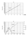
- FIG. 4 is a diagram showing an example of an increasing function of the power level of an RF pulse and a reflected wave in a reference example during the ramp-up period S32.
- FIG. 5 is a diagram showing an example of an increasing function of the power level of the RF pulse and reflected waves in the embodiment during the ramp-up period S32.
- experimental results are shown when HF with a frequency of 40 MHz is used.
- the horizontal axis in FIGS. 4(a), 5(a), and (b) shows the number of times the power level of the RF pulse (HF pulse) is increased stepwise, and the vertical axis shows the power (W).
- the RF power source 31 was controlled so that the HF power monotonically increased during the ramp-up period S32, as shown by Pw(ref) in FIG. 4(a).
- "c” is a parameter that controls the slope (c>0) of the straight line of the HF power Pw(ref) shown in FIG. 4(a), that is, the speed of variation of the power Pw(ref) during the ramp-up period.
- "d” is the HF power level at the start of the ramp-up period, that is, the HF power level when the horizontal axis is 0.
- the number of times on the horizontal axis in FIG. 4(a) is from the start of supply of pulsed HF power (start of the ramp-up period) shown at time t3 in FIG . This is the number of times the HF power level is increased in stages up to the end of the period.
- the HF power Pw (ref) of the reference example is controlled from 100 W set at the supply start time (time t 3 ) to 1000 W at the peak output time (time t 4 ).
- FIG. 4(b) shows a reflected wave R(ref) generated as a result of controlling the HF power Pw(ref) in the reference example shown in FIG. 4(a).
- FIG. 4(b) indicates time, and corresponds to the number of times on the horizontal axis in FIG. 4(a). For example, “0 times" on the horizontal axis in FIG. 4(a) corresponds to “26 seconds” on the horizontal axis in FIG. 4(b), and “10 times” on the horizontal axis in FIG. 4(a) corresponds to "26 seconds” on the horizontal axis in FIG. This corresponds to "28 seconds” on the horizontal axis in (b).
- the vertical axis (right) indicates the HF reflected wave (%), and the vertical axis (left) indicates the HF power (progressive wave power) (W).
- the HF reflected wave (%) is the ratio of the HF reflected wave to the supplied HF traveling wave expressed as a percentage (%).
- the percentage of the HF reflected wave R (ref) was high at about 15% at the beginning of the ramp-up period S32 (26 seconds to 27 seconds), but after 27 seconds, it was almost It became 0%. That is, in the reference example, it was found that HF reflected waves were likely to occur at the beginning of the ramp-up period S32.
- the HF power was controlled using Pw (recipe) in FIG. 5(a) as the target value, and the actual value (not shown) of the HF power during the ramp-up period S32 when three substrates W were actually processed was measured. .
- the coefficient "a” is a parameter that controls the speed of variation of the HF power Pw during the ramp-up period.
- A is the level of RF power at the start of the ramp-up period, and t indicates the time from the start of the ramp-up period.
- the number of times on the horizontal axis in FIGS. 5(a) and (b) is the HF power consumption during the time from the ramp-up start point shown at time t3 in FIG. 3 to the ramp-up end point (peak point) shown at time t4 . This is the number of times to raise the level step by step.
- the HF power Pw of the embodiment is controlled from 100 W set at the supply start time (time t 3 ) to 1000 W set at the peak output time (time t 4 ).
- FIG. 5(c) shows the reflected wave R generated as a result of controlling the HF power Pw in the embodiment shown in FIG. 5(b).
- the vertical axis (right) in FIG. 5(c) indicates the HF reflected wave (%), and the vertical axis (left) indicates the HF power (progressive wave power) (W).
- the HF reflected wave (%) is the ratio of the HF reflected wave to the supplied HF traveling wave expressed as a percentage (%).
- the percentage of the reflected wave R of the HF power is 5% or less, and compared to the reference example of FIG. 4(b), the ramp-up period S32 (26.8 seconds to 28.8 seconds
- the reflected waves decreased over the entire period (seconds). That is, in the embodiment, it has been found that HF reflected waves are unlikely to occur during the ramp-up period S32. In other words, in the reference example, a large reflected wave is generated in the first half of the ramp-up period S32 when the HF power is low, and in the embodiment, a small reflected wave is generated throughout the ramp-up period S32.
- the maximum value of the reflected wave is reduced to 5% or less of the HF traveling wave, and plasma load fluctuation is reduced.
- HF power is simply increased in the ramp-up period S32, reflected waves are likely to occur when the power is low (see FIG. 4(b)). For example, this is because the plasma tends to become unstable when the HF power is low (for example, 400 W or less).
- the HF power is low (for example, 400 W or less) at which the plasma tends to become unstable, the HF power The speed of fluctuation can be slowed down.
- the impedance matching accuracy between the RF power source 31 and the load is improved, thereby suppressing reflected waves of the HF power, Plasma load fluctuations can be suppressed.
- the HF pulse was exponentially increased as an example of the RF power in the ramp-up period S32, but the same effect can be obtained by controlling the LF power in the same way. That is, by increasing the LF pulse exponentially in the ramp-up period S32, reflected waves can be reduced, and plasma load fluctuations can be suppressed.
- the RF power is not limited to being increased exponentially in the ramp-up period S32.
- the RF power source 31 may be controlled so that the increasing function of the power level from the start of supply of RF pulses to the peak point becomes a downwardly convex function.
- the speed of fluctuation of the RF power can be slowed down, the reflected waves of the RF power can be suppressed, and the load fluctuation of the plasma can be suppressed.
- controlling the RF power so that the increasing function becomes a downwardly convex function means that when the horizontal axis is time and the vertical axis is RF power, the power when the RF pulse is on or high is downward. It becomes convex and increases the RF power over time.
- the increasing function of the power level from the start point of RF power supply (for example, time t 3 in FIG. 3 ) to the peak point (for example, time t 4 in FIG. 3) is expressed by the following equations (1) and (2).
- the RF power supply 31 is controlled so as to satisfy the function shown in (). The explanation will be divided into cases (i) and (ii).
- the RF power source 31 may be controlled so that only the HF power during the ramp-up period S32 becomes a downwardly convex function. In this case, the LF power during the ramp-up period S32 may increase monotonically. Further, the RF power source 31 may be controlled so that only the LF power during the ramp-up period S32 becomes a downwardly convex function. In this case, the HF power during the ramp-up period S32 may increase monotonically. Further, the RF power source 31 may be controlled so that both the HF power and the LF power in the ramp-up period S32 have a downwardly convex function.
- FIG. 6 is a diagram showing an example of a reduction function of the power level of the RF pulse and reflected waves in the embodiment during the ramp-down period S34.
- experimental results are shown when HF with a frequency of 40 MHz is used.
- the control device 2 adjusts the HF power so that it follows the curve set in the recipe during the ramp-down period S34, as shown in Pw (recipe) in FIG. 6(a).
- the RF power source 31 was controlled so that the HF power decreased exponentially.
- the HF power was controlled using Pw (recipe) in FIG. 6(a) as the target value, and the actual value (not shown) of the HF power during the ramp-down period S34 when three substrates W were actually processed was measured. .
- the coefficient "b" is a parameter that controls the speed of variation of the HF power Pw during the ramp-down period.
- “B” is the level of RF power at the beginning of the ramp-down period, and t indicates the time from the beginning of the ramp-down period.
- the number of times on the horizontal axis in FIGS. 6(a) and (b) is from the peak end point (rampdown start point) shown at time t5 in FIG. 3 to the supply end point (rampdown end point) shown at time t6 in FIG. This is the number of times the HF power level is gradually lowered over time.
- the HF power Pw of the embodiment is controlled from 1000 W set at the peak end time (time t 5 ) to 100 W at the supply end time (time t 6 ).
- FIG. 6(c) shows the reflected wave R generated as a result of controlling the HF power Pw in the embodiment shown in FIG. 6(b).
- FIG. 6(c) indicates time, and corresponds to the number of times on the horizontal axis in FIG. 6(b).
- the vertical axis (right) indicates the HF reflected wave (%)
- the vertical axis (left) indicates the HF power (progressive wave power) (W).
- the HF reflected wave (%) is the ratio of the HF reflected wave to the supplied HF traveling wave expressed as a percentage (%).
- the percentage R of reflected waves of HF power is 17.5% or less, and there are few reflected waves throughout the ramp-down period S34.
- the maximum value of the reflected wave is reduced to 17.5% or less of the HF traveling wave in the ramp-down period S34, and the plasma load fluctuation is reduced.
- HF power is simply decreased in the ramp-down period S34, reflected waves are likely to occur when the power is low. For example, this is because the plasma tends to become unstable when the HF power is low (for example, 400 W or less).
- the HF power is low (for example, 400 W or less) at which the plasma tends to become unstable
- the HF power The speed of fluctuation can be slowed down.
- the impedance matching accuracy between the RF power source 31 and the load is improved, thereby suppressing reflected waves of the HF power, Plasma load fluctuations can be suppressed.
- the HF power is exponentially reduced as an example of RF power in the ramp-down period S34, but the same effect can be obtained by controlling the LF power in the same manner. That is, by exponentially decreasing the LF pulse during the ramp-down period S34, reflected waves can be reduced, and plasma load fluctuations can be suppressed.
- the RF power is not limited to decreasing exponentially in the ramp-down period S34.
- the RF power source 31 may be controlled so that the decreasing function of the power level from the end of the peak of the RF pulse to the end of supply becomes a downwardly convex function. Thereby, reflected waves of RF power can be suppressed, and plasma load fluctuations can be suppressed.
- controlling the RF power so that the decreasing function becomes a downwardly convex function means that when the horizontal axis is time and the vertical axis is RF power, the power when the RF pulse is on or high is downward. It is to become convex and reduce RF power over time.
- the power level decreasing function from the end of the peak of RF power (for example, time t 5 in FIG. 3) to the end of supply (for example, time t 6 in FIG. 3) is expressed by the following equations (3) and (4).
- the RF power supply 31 is controlled so as to satisfy the function shown in ().
- B indicates the RF power level at the end of the peak of RF power.
- t indicates the time from the end of the peak of RF power.
- Pw(t) indicates the RF power level at time t from the peak end point.
- P min indicates the minimum value of the RF power level.
- t max indicates the time from the end of the peak of RF power to the end of supply.
- the RF power source 31 may be controlled so that only the HF power in the ramp-down period S34 becomes a downwardly convex function.
- the LF power during the ramp-down period S34 may monotonically decrease.
- the RF power source 31 may be controlled so that only the LF power during the ramp-down period S34 becomes a downwardly convex function.
- the HF power during the ramp-down period S34 may monotonically decrease.
- the RF power source 31 may be controlled so that both the HF power and the LF power in the ramp-down period S34 become a downwardly convex function.
- FIG. 1 Another example in which the power level increasing function from the start of supply of pulsed RF power to the peak point is a downwardly convex function may include a case where the slope of the convex function changes midway. For example, from the start of RF power supply (for example, time t 3 in FIG. 3 ) to a time (time tt) halfway between the peak point (for example, time t 4 in FIG. 3), there is a gentle slope (slope a1). ) is the straight line. From time tt to the peak point (for example, time t 4 in FIG. 3), a straight line may be formed with a slope a2 different from the slope a1, and the slope may be changed.
- the slope a1 is set to a smaller value than the slope a2, making it a downwardly convex function.
- the slope a1 is set to a smaller value than the slope a2, making it a downwardly convex function.
- the slope is controlled by controlling the slope to a downwardly convex increasing function with a gentle slope for a predetermined period of time (until time tt) from the start of RF power supply, reflected waves of RF power are suppressed and the ramp-up period is controlled. Plasma load fluctuations can be suppressed.
- the straight line from the start point of RF power supply to the peak point point is described as a combination of straight lines whose slope changes at time tt, but the present invention is not limited to this.
- FIG. 2 Another example in which the decreasing function of the power level from the peak end point of pulsed RF power (ramp down start point) to the supply end point (ramp down end point) is a downwardly convex function. It may also include a case where the slope changes.
- a straight line with an inclination a3 is defined from the end of the peak of RF power (for example, time t 5 in FIG. 3) to a time (time tk) halfway between the end of supply (for example, time t 6 in FIG. 3). From time tk to the end of supply (for example, time t 6 in FIG. 3), the straight line may have a slope a4 different from a3, and the slope may be changed.
- the slope a4 is set to a smaller value than the slope a3, making it a downwardly convex function.
- the straight line from the end of the peak of RF power to the end of supply is described as a combination of straight lines whose slope changes at time tk, but the present invention is not limited to this. It is not limited to a straight line, but may be a combination of a straight line and/or a curved line, as long as the slope can be made gentle for a while before the RF power supply ends and controlled to a downwardly convex decreasing function.
- plasma load fluctuations can be suppressed.
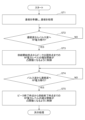
- FIG. 7 is a flowchart illustrating an example of the plasma processing method according to the embodiment.
- the power supply system includes an RF power supply 31 that supplies pulsed RF power to the plasma processing chamber 10 and/or the substrate support 11, and a control device 2 that controls the supply of the pulsed RF power.
- the RF power described below may be HF power, LF power, HF power and LF power.
- step ST1 the control device 2 prepares a substrate on the substrate support section 11, supplies a processing gas from the gas supply section 20 into the plasma processing chamber 10, and uses continuous wave RF from the RF power source 31. Control to supply power. As a result, the processing gas is turned into plasma, and the substrate is subjected to plasma processing.
- step ST2 the control device 2 determines whether to shift the RF power from continuous waves to pulse waves. If the control device 2 determines that the RF power is not to be shifted from a continuous wave to a pulse wave (NO in step ST2), it repeats the determination process in step ST2 until it determines YES in step ST2.
- control device 2 determines that the RF power is to be shifted from a continuous wave to a pulse wave
- the control device 2 proceeds to step ST3, and controls the control device 2 so that the increasing function of the RF power from the start of supply of RF pulses to the point of peak occurrence becomes a downwardly convex function.
- the RF power supply 31 is controlled to proceed to step ST4.
- step ST4 the control device 2 determines whether the RF power shifts from a pulse wave to a continuous wave. If the control device 2 determines that the RF power does not shift from a pulse wave to a continuous wave (NO in step ST4), it repeats the determination process in step ST4 until it determines YES in step ST4.
- control device 2 determines that the RF power shifts from a pulse wave to a continuous wave
- the control device 2 proceeds to step ST5, and the decreasing function of the RF power level from the end of the peak of the RF pulse to the end of supply becomes a downwardly convex function.
- the RF power supply 31 is controlled as shown in FIG. 2, and the process proceeds to the next step.
- reflected waves of RF power can be suppressed, and plasma load fluctuations during the ramp-up period and/or the ramp-down period can be suppressed.
- the plasma processing apparatus, power supply system, and plasma processing method according to the embodiments disclosed herein are illustrative in all respects and should not be considered restrictive.
- the embodiments can be modified and improved in various ways without departing from the scope and spirit of the appended claims.
- the matters described in the plurality of embodiments described above may be configured in other ways without being inconsistent, and may be combined without being inconsistent.
- the plasma processing apparatus of the present disclosure includes an Atomic Layer Deposition (ALD) apparatus, Capacitively Coupled Plasma (CCP), Inductively Coupled Plasma (ICP), Radial Line Slot Antenna (RLSA), Electron Cyclotron Resonance Plasma (ECR), Helicon Wave Plasma ( Applicable to any type of device (HWP).
- ALD Atomic Layer Deposition
- CCP Capacitively Coupled Plasma
- ICP Inductively Coupled Plasma
- RLSA Radial Line Slot Antenna
- ECR Electron Cyclotron Resonance Plasma
- HWP Helicon Wave Plasma
- Plasma processing apparatus 2 Control device 2a Computer 2a1 Processing section 2a2 Storage section 2a3 Communication interface 10 Plasma processing chamber 11 Substrate support section 13 Shower head 21 Gas source 20 Gas supply section 30 Power supply 31 RF power supply 31a First RF generation section 31b No. 2 RF generation section 32a First DC generation section 32b Second DC generation section 40 Exhaust system 111 Main body section 112 Ring assembly
Landscapes
- Chemical & Material Sciences (AREA)
- Engineering & Computer Science (AREA)
- Physics & Mathematics (AREA)
- Plasma & Fusion (AREA)
- Analytical Chemistry (AREA)
- Mechanical Engineering (AREA)
- Chemical Kinetics & Catalysis (AREA)
- Materials Engineering (AREA)
- General Chemical & Material Sciences (AREA)
- Metallurgy (AREA)
- Organic Chemistry (AREA)
- Electromagnetism (AREA)
- Spectroscopy & Molecular Physics (AREA)
- Drying Of Semiconductors (AREA)
- Plasma Technology (AREA)
- Chemical Vapour Deposition (AREA)
Abstract
Description
本開示は、プラズマ処理装置、電源システム及びプラズマ処理方法に関する。 The present disclosure relates to a plasma processing apparatus, a power supply system, and a plasma processing method.
例えば、特許文献1は、SiC膜を下地膜としてSiOC系のLow-k膜等をエッチングする方法を提供している。このエッチング方法では、RF電源の電力を第2の電力の値までスローアップし、その後電力変調モードにしている。また、可変直流電源の直流電圧をスローアップしている。これらいずれかをこのようにスローアップすることにより、ウェハや電源へのダメージを軽減することができる。 For example, Patent Document 1 provides a method of etching a SiOC-based low-k film or the like using a SiC film as a base film. In this etching method, the power of the RF power source is slowed up to a second power value and then placed in a power modulation mode. Additionally, the DC voltage of the variable DC power supply is slowed down. By slowing down either of these, damage to the wafer or power supply can be reduced.
本開示は、プラズマの負荷変動を抑えることができる技術を提供する。 The present disclosure provides a technique that can suppress plasma load fluctuations.
本開示の一の態様によれば、プラズマ処理チャンバと、前記プラズマ処理チャンバに設けられ、基板が載置される基板支持部と、前記プラズマ処理チャンバに処理ガスを供給するガス供給部と、前記プラズマ処理チャンバ及び/又は前記基板支持部にパルス化されたRF電力を供給し、前記処理ガスのプラズマを生成するRF電源と、パルス化された前記RF電力の供給を制御する制御装置と、を有し、前記制御装置は、パルス化された前記RF電力の供給開始時点からピーク出現時点までの電力レベルの増加関数が下に凸関数となる、及び/又は、パルス化された前記RF電力のピーク終了時点から供給終了時点までの電力レベルの減少関数が下に凸関数となるように前記RF電源を制御する、プラズマ処理装置が提供される。 According to one aspect of the present disclosure, a plasma processing chamber, a substrate support section provided in the plasma processing chamber and on which a substrate is placed, a gas supply section supplying a processing gas to the plasma processing chamber, and the an RF power source that supplies pulsed RF power to the plasma processing chamber and/or the substrate support to generate plasma of the processing gas; and a control device that controls the supply of the pulsed RF power. and/or the control device is configured such that an increasing function of the power level from the start point of supply of the pulsed RF power to the point of peak occurrence is a downwardly convex function, and/or the control device A plasma processing apparatus is provided in which the RF power source is controlled so that a decreasing function of the power level from a peak end point to a supply end point is a downwardly convex function.
一の側面によれば、プラズマの負荷変動を抑えることができる。 According to one aspect, plasma load fluctuations can be suppressed.
以下、図面を参照して本開示を実施するための形態について説明する。各図面において、同一構成部分には同一符号を付し、重複した説明を省略する場合がある。 Hereinafter, embodiments for implementing the present disclosure will be described with reference to the drawings. In each drawing, the same components are given the same reference numerals, and redundant explanations may be omitted.
本明細書において平行、直角、直交、水平、垂直、上下、左右などの方向には、実施形態の効果を損なわない程度のずれが許容される。角部の形状は、直角に限られず、弓状に丸みを帯びてもよい。平行、直角、直交、水平、垂直、円、一致には、略平行、略直角、略直交、略水平、略垂直、略円、略一致が含まれてもよい。 In this specification, deviations in directions such as parallel, perpendicular, perpendicular, horizontal, perpendicular, up and down, left and right are allowed to the extent that the effects of the embodiments are not impaired. The shape of the corner portion is not limited to a right angle, but may be rounded in an arcuate shape. Parallel, perpendicular, orthogonal, horizontal, perpendicular, circular, and coincident may include substantially parallel, substantially perpendicular, substantially orthogonal, substantially horizontal, substantially perpendicular, substantially circular, and substantially coincident.
[プラズマ処理装置]
以下に、プラズマ処理装置の構成例について説明する。図1は、容量結合型のプラズマ処理装置の構成例を説明するための図である。
[Plasma processing equipment]
An example of the configuration of the plasma processing apparatus will be described below. FIG. 1 is a diagram for explaining a configuration example of a capacitively coupled plasma processing apparatus.
プラズマ処理装置1は、容量結合型のプラズマ処理装置であり、プラズマ処理チャンバ10、ガス供給部20、電源30、排気システム40及び制御装置2を含む。また、プラズマ処理装置1は、基板支持部11及びガス導入部を含む。ガス導入部は、少なくとも1つの処理ガスをプラズマ処理チャンバ10内に導入するように構成される。ガス導入部は、シャワーヘッド13を含む。基板支持部11は、プラズマ処理チャンバ10内に配置される。シャワーヘッド13は、基板支持部11の上方に配置される。一実施形態において、シャワーヘッド13は、プラズマ処理チャンバ10の天部(ceiling)の少なくとも一部を構成する。プラズマ処理チャンバ10は、シャワーヘッド13、プラズマ処理チャンバ10の側壁10a及び基板支持部11により規定されたプラズマ処理空間10sを有する。プラズマ処理チャンバ10は、少なくとも1つの処理ガスをプラズマ処理空間10sに供給するための少なくとも1つのガス供給口と、プラズマ処理空間からガスを排出するための少なくとも1つのガス排出口とを有する。プラズマ処理チャンバ10は接地される。シャワーヘッド13及び基板支持部11とプラズマ処理チャンバ10の筐体とは電気的に絶縁される。
The plasma processing apparatus 1 is a capacitively coupled plasma processing apparatus, and includes a
基板支持部11は、本体部111及びリングアセンブリ112を含む。本体部111は、基板Wを支持するための中央領域111aと、リングアセンブリ112を支持するための環状領域111bとを有する。ウェハは基板Wの一例である。本体部111の環状領域111bは、平面視で本体部111の中央領域111aを囲んでいる。基板Wは、本体部111の中央領域111a上に配置され、リングアセンブリ112は、本体部111の中央領域111a上の基板Wを囲むように本体部111の環状領域111b上に配置される。従って、中央領域111aは、基板Wを支持するための基板支持面とも呼ばれ、環状領域111bは、リングアセンブリ112を支持するためのリング支持面とも呼ばれる。
The
一実施形態において、本体部111は、基台1110及び静電チャック1111を含む。基台1110は、導電性部材を含む。基台1110の導電性部材は下部電極として機能し得る。静電チャック1111は、基台1110の上に配置される。静電チャック1111は、セラミック部材1111aとセラミック部材1111a内に配置される静電電極1111bとを含む。セラミック部材1111aは、中央領域111aを有する。一実施形態において、セラミック部材1111aは、環状領域111bも有する。なお、環状静電チャックや環状絶縁部材のような、静電チャック1111を囲む他の部材が環状領域111bを有してもよい。この場合、リングアセンブリ112は、環状静電チャック又は環状絶縁部材の上に配置されてもよく、静電チャック1111と環状絶縁部材の両方の上に配置されてもよい。また、後述するRF(Radio Frequency)電源31及び/又はDC(Direct Current)電源32に結合される少なくとも1つのRF/DC電極がセラミック部材1111a内に配置されてもよい。この場合、少なくとも1つのRF/DC電極が下部電極として機能する。後述するバイアスRF信号及び/又はDC信号が少なくとも1つのRF/DC電極に供給される場合、RF/DC電極はバイアス電極とも呼ばれる。なお、基台1110の導電性部材と少なくとも1つのRF/DC電極とが複数の下部電極として機能してもよい。また、静電電極1111bが下部電極として機能してもよい。従って、基板支持部11は、少なくとも1つの下部電極を含む。
In one embodiment, the
リングアセンブリ112は、1又は複数の環状部材を含む。一実施形態において、1又は複数の環状部材は、1又は複数のエッジリングと少なくとも1つのカバーリングとを含む。エッジリングは、導電性材料又は絶縁材料で形成され、カバーリングは、絶縁材料で形成される。
また、基板支持部11は、静電チャック1111、リングアセンブリ112及び基板のうち少なくとも1つをターゲット温度に調節するように構成される温調モジュールを含んでもよい。温調モジュールは、ヒータ、伝熱媒体、流路1110a、又はこれらの組み合わせを含んでもよい。流路1110aには、ブラインやガスのような伝熱流体が流れる。一実施形態において、流路1110aが基台1110内に形成され、1又は複数のヒータが静電チャック1111のセラミック部材1111a内に配置される。また、基板支持部11は、基板Wの裏面と中央領域111aとの間の間隙に伝熱ガスを供給するように構成された伝熱ガス供給部を含んでもよい。
Further, the
シャワーヘッド13は、ガス供給部20からの少なくとも1つの処理ガスをプラズマ処理空間10s内に導入するように構成される。シャワーヘッド13は、少なくとも1つのガス供給口13a、少なくとも1つのガス拡散室13b、及び複数のガス導入口13cを有する。ガス供給口13aに供給された処理ガスは、ガス拡散室13bを通過して複数のガス導入口13cからプラズマ処理空間10s内に導入される。また、シャワーヘッド13は、少なくとも1つの上部電極を含む。なお、ガス導入部は、シャワーヘッド13に加えて、側壁10aに形成された1又は複数の開口部に取り付けられる1又は複数のサイドガス注入部(SGI:Side Gas Injector)を含んでもよい。
The
ガス供給部20は、少なくとも1つのガスソース21及び少なくとも1つの流量制御器22を含んでもよい。一実施形態において、ガス供給部20は、少なくとも1つの処理ガスを、それぞれに対応のガスソース21からそれぞれに対応の流量制御器22を介してシャワーヘッド13に供給するように構成される。各流量制御器22は、例えばマスフローコントローラ又は圧力制御式の流量制御器を含んでもよい。さらに、ガス供給部20は、少なくとも1つの処理ガスの流量を変調又はパルス化する1又はそれ以上の流量変調デバイスを含んでもよい。
The
電源30は、少なくとも1つのインピーダンス整合回路を介してプラズマ処理チャンバ10に結合されるRF電源31を含む。RF電源31は、少なくとも1つのRF信号(RF電力)を少なくとも1つの下部電極及び/又は少なくとも1つの上部電極に供給するように構成される。これにより、プラズマ処理空間10sに供給された少なくとも1つの処理ガスからプラズマが形成される。従って、RF電源31は、プラズマ処理チャンバ10において1又はそれ以上の処理ガスからプラズマを生成するように構成されるプラズマ生成部の少なくとも一部として機能し得る。また、バイアスRF信号を少なくとも1つの下部電極に供給することにより、基板Wにバイアス電位が発生し、形成されたプラズマ中のイオン成分を基板Wに引き込むことができる。
一実施形態において、RF電源31は、第1のRF生成部31a及び第2のRF生成部31bを含む。第1のRF生成部31aは、少なくとも1つのインピーダンス整合回路を介して少なくとも1つの下部電極及び/又は少なくとも1つの上部電極に結合され、プラズマ生成用のソースRF信号(ソースRF電力)を生成するように構成される。一実施形態において、ソースRF信号は、10MHz~150MHzの範囲内の周波数を有する。一実施形態において、第1のRF生成部31aは、異なる周波数を有する複数のソースRF信号を生成するように構成されてもよい。生成された1又は複数のソースRF信号は、少なくとも1つの下部電極及び/又は少なくとも1つの上部電極に供給される。
In one embodiment, the
第2のRF生成部31bは、少なくとも1つのインピーダンス整合回路を介して少なくとも1つの下部電極に結合され、バイアスRF信号(バイアスRF電力)を生成するように構成される。バイアスRF信号の周波数は、ソースRF信号の周波数と同じであっても異なっていてもよい。一実施形態において、バイアスRF信号は、ソースRF信号の周波数よりも低い周波数を有する。一実施形態において、バイアスRF信号は、100kHz~60MHzの範囲内の周波数を有する。一実施形態において、第2のRF生成部31bは、異なる周波数を有する複数のバイアスRF信号を生成するように構成されてもよい。生成された1又は複数のバイアスRF信号は、少なくとも1つの下部電極に供給される。また、種々の実施形態において、ソースRF信号及びバイアスRF信号のうち少なくとも1つがパルス化されてもよい。
The second
また、電源30は、プラズマ処理チャンバ10に結合されるDC電源32を含んでもよい。DC電源32は、第1のDC生成部32a及び第2のDC生成部32bを含む。一実施形態において、第1のDC生成部32aは、少なくとも1つの下部電極に接続され、第1のDC信号を生成するように構成される。生成された第1のバイアスDC信号は、少なくとも1つの下部電極に印加される。一実施形態において、第2のDC生成部32bは、少なくとも1つの上部電極に接続され、第2のDC信号を生成するように構成される。生成された第2のDC信号は、少なくとも1つの上部電極に印加される。
種々の実施形態において、第1及び第2のDC信号のうち少なくとも1つがパルス化されてもよい。この場合、電圧パルスのシーケンスが少なくとも1つの下部電極及び/又は少なくとも1つの上部電極に印加される。電圧パルスは、矩形、台形、三角形又はこれらの組み合わせのパルス波形を有してもよい。一実施形態において、DC信号から電圧パルスのシーケンスを生成するための波形生成部が第1のDC生成部32aと少なくとも1つの下部電極との間に接続される。従って、第1のDC生成部32a及び波形生成部は、電圧パルス生成部を構成する。第2のDC生成部32b及び波形生成部が電圧パルス生成部を構成する場合、電圧パルス生成部は、少なくとも1つの上部電極に接続される。電圧パルスは、正の極性を有してもよく、負の極性を有してもよい。また、電圧パルスのシーケンスは、1周期内に1又は複数の正極性電圧パルスと1又は複数の負極性電圧パルスとを含んでもよい。なお、第1及び第2のDC生成部32a,32bは、RF電源31に加えて設けられてもよく、第1のDC生成部32aが第2のRF生成部31bに代えて設けられてもよい。
In various embodiments, at least one of the first and second DC signals may be pulsed. In this case, a sequence of voltage pulses is applied to at least one lower electrode and/or at least one upper electrode. The voltage pulse may have a pulse waveform that is rectangular, trapezoidal, triangular, or a combination thereof. In one embodiment, a waveform generator for generating a sequence of voltage pulses from a DC signal is connected between the
排気システム40は、例えばプラズマ処理チャンバ10の底部に設けられたガス排出口10eに接続され得る。排気システム40は、圧力調整弁及び真空ポンプを含んでもよい。圧力調整弁によって、プラズマ処理空間10s内の圧力が調整される。真空ポンプは、ターボ分子ポンプ、ドライポンプ又はこれらの組み合わせを含んでもよい。
The
制御装置2は、本開示において述べられる種々の工程をプラズマ処理装置1に実行させるコンピュータ実行可能な命令を処理する。制御装置2は、ここで述べられる種々の工程を実行するようにプラズマ処理装置1の各要素を制御するように構成され得る。例えば、制御装置2は、連続波からパルス波及びパルス波から連続波に移行する際のRF電力の供給を制御してもよい。一実施形態において、制御装置2の一部又は全てがプラズマ処理装置1に含まれてもよい。制御装置2は、処理部2a1、記憶部2a2及び通信インターフェース2a3を含んでもよい。制御装置2は、例えばコンピュータ2aにより実現される。処理部2a1は、記憶部2a2からプログラムを読み出し、読み出されたプログラムを実行することにより種々の制御動作を行うように構成され得る。このプログラムは、予め記憶部2a2に格納されていてもよく、必要なときに、媒体を介して取得されてもよい。取得されたプログラムは、記憶部2a2に格納され、処理部2a1によって記憶部2a2から読み出されて実行される。媒体は、コンピュータ2aに読み取り可能な種々の記憶媒体であってもよく、通信インターフェース2a3に接続されている通信回線であってもよい。処理部2a1は、CPU(Central Processing Unit)であってもよい。記憶部2a2は、RAM(Random Access Memory)、ROM(Read Only Memory)、HDD(Hard Disk Drive)、SSD(Solid State Drive)、又はこれらの組み合わせを含んでもよい。通信インターフェース2a3は、LAN(Local Area Network)等の通信回線を介してプラズマ処理装置1との間で通信してもよい。
The
[RF電力の移行シーケンス]
RF電力が連続波からパルス波へ移行するとき、及び、パルス波から連続波へ移行するときのシーケンスについて、図2及び図3を参照しながら説明する。図2は、参考例のRF電力の連続波とパルス波の移行シーケンス例を示す図である。図3は、実施形態に係るRF電力の連続波とパルス波の移行シーケンス例を示す図である。なお、図2及び図3にはRF電力の制御条件のみが示され、処理ガスやチャンバ内の圧力等の制御条件については示されていないが、図2及び図3の時刻t0~時刻t6の期間及び時刻t6以降の期間、本実施形態の基板処理に使用するレシピに設定された制御条件に従い、基板Wのプラズマ処理が行われる。
[RF power transition sequence]
The sequences when the RF power changes from a continuous wave to a pulsed wave and from a pulsed wave to a continuous wave will be described with reference to FIGS. 2 and 3. FIG. 2 is a diagram showing an example of a transition sequence between a continuous wave and a pulse wave of RF power according to a reference example. FIG. 3 is a diagram illustrating an example of a transition sequence between a continuous wave and a pulse wave of RF power according to the embodiment. Note that FIGS. 2 and 3 only show the control conditions for the RF power, and do not show the control conditions for the processing gas, the pressure in the chamber, etc., but from time t 0 to time t in FIGS. 2 and 3 6 and the period after time t6 , plasma processing of the substrate W is performed according to the control conditions set in the recipe used for substrate processing of this embodiment.
以下、RF電力のパルス波を「RFパルス」ともいう。また、RF電力のうち、RFソース電力を「HF」又は「HF電力」ともいい、HFのパルス波を「HFパルス」ともいう。また、RFバイアス電力を「LF」又は「LF電力」ともいい、LFのパルス波を「LFパルス」ともいう。図2及び図3は、基板にプラズマ処理を行うときのHF及びLFの供給シーケンスの一例を示し、各図の横軸は時間を示し、縦軸は電力(ワット)を示す。なお、図2及び図3に記載の電力値は一例であり、これに限らない。図2及び図3のいずれも、時刻t0~時刻t1の期間S1は、HF及びLFのいずれも連続波であり、連続的に各電力を供給し、処理ガスのプラズマが生成される。時刻t1~時刻t2の期間S2は、HF及びLFのいずれも期間S1よりも電力レベルが低い連続波の電力を供給し、プラズマの生成を続ける。時刻t2でHF及びLFのいずれも連続波からパルス波に移行する。時刻t2~時刻t6の期間S3は、HF及びLFのいずれもパルス波の電力を供給する。期間S3中、HFパルスはハイ(High)及びロー(Low)の2レベルの電力を供給し、LFパルスはオン(On)及びオフ(Off)の2レベルの電力を供給する。ただし、HFパルス及びLFパルスは、ハイ及びローの2レベルの電力、オン及びオフの2レベルの電力のいずれのパルス波であってもよい。 Hereinafter, the pulse wave of RF power will also be referred to as "RF pulse". Further, among the RF power, the RF source power is also referred to as "HF" or "HF power", and the HF pulse wave is also referred to as "HF pulse". Further, the RF bias power is also referred to as "LF" or "LF power", and the LF pulse wave is also referred to as "LF pulse". 2 and 3 show an example of a supply sequence of HF and LF when performing plasma processing on a substrate, and in each figure, the horizontal axis shows time and the vertical axis shows power (watts). Note that the power values shown in FIGS. 2 and 3 are merely examples, and the power values are not limited thereto. In both FIGS. 2 and 3, during the period S1 from time t 0 to time t 1 , both HF and LF are continuous waves, and each power is continuously supplied to generate plasma of the processing gas. During the period S2 from time t 1 to time t 2 , both HF and LF supply continuous wave power having a lower power level than the period S1 to continue generating plasma. At time t2 , both HF and LF transition from continuous waves to pulse waves. During the period S3 from time t 2 to time t 6 , both HF and LF supply pulse wave power. During the period S3, the HF pulse supplies two levels of power, high and low, and the LF pulse supplies two levels of power, on and off. However, the HF pulse and the LF pulse may be pulse waves with two levels of power, high and low, or two levels of power, on and off.
期間S3中、時刻t2~時刻t3の期間S31において、HFパルス及びLFパルスのいずれもハイ又はオン時の電力レベルはフラット(一定)である。時刻t3~時刻t4の期間S32では、HFパルス及びLFパルスの電力レベルは増加する。時刻t4にHFパルス及びLFパルスの電力レベルはピーク(最大)に到達する。そして、時刻t4~時刻t5の期間S33は、HFパルス及びLFパルスの電力レベルはピーク値(最大値)を維持する。時刻t5~時刻t6の期間S34は、HFパルス及びLFパルスの電力レベルは減少する。時刻t6でHF及びLFのいずれもパルス波から連続波に移行し、時刻t6以降の期間S4は、HF及びLFのいずれも連続波となる。 During period S3, during period S31 from time t 2 to time t 3 , the power level of both the HF pulse and the LF pulse when they are high or on is flat (constant). In period S32 from time t 3 to time t 4 , the power levels of the HF pulse and the LF pulse increase. At time t4 , the power levels of the HF and LF pulses reach their peak (maximum). Then, during the period S33 from time t 4 to time t 5 , the power levels of the HF pulse and the LF pulse maintain the peak value (maximum value). During the period S34 from time t5 to time t6 , the power levels of the HF pulse and the LF pulse decrease. At time t6 , both HF and LF transition from pulse waves to continuous waves, and in the period S4 after time t6 , both HF and LF become continuous waves.
図2及び図3のいずれも、期間S32はHFパルス及びLFパルスが同期して増加する期間であり、本明細書では「ランプアップ(Ramp up)の期間」という。期間S34はHFパルス及びLFパルスが同期して減少する期間であり、本明細書では「ランプダウン(Ramp down)の期間」という。ただし、HFパルス及びLFパルスの期間S32及び期間S34の開始時点は、完全に同期せずにずれ(オフセット)があってもよい。 In both FIGS. 2 and 3, the period S32 is a period in which the HF pulse and the LF pulse increase synchronously, and is referred to herein as a "ramp up period." The period S34 is a period in which the HF pulse and the LF pulse decrease synchronously, and is referred to herein as a "ramp down period." However, the starting points of the period S32 and the period S34 of the HF pulse and the LF pulse may not be completely synchronized but may have a shift (offset).
図2及び図3のいずれも、期間S2から期間S3へ移行するとき、すなわち、HF及びLFが連続波からパルス波に移行するとき、プラズマは引き続き生成(着火)された状態であり、プラズマは消失しない。同様に、期間S3から期間S4へ移行するとき、すなわち、HF及びLFがパルス波から連続波に移行するとき、プラズマは生成された状態であり、プラズマは消失しない。 In both FIGS. 2 and 3, when transitioning from period S2 to period S3, that is, when HF and LF transition from continuous waves to pulse waves, plasma continues to be generated (ignited), and the plasma continues to be generated (ignited). It doesn't disappear. Similarly, when transitioning from period S3 to period S4, that is, when HF and LF transition from pulse waves to continuous waves, plasma is in a generated state and does not disappear.
図2及び図3のいずれも、ランプアップ期間S32では、HFパルス及びLFパルスの供給開始時点(ランプアップ開始時点、時刻t3)からピーク出現時点(ランプアップ終了時点、時刻t4)までの電力レベルは、増加関数である。ただし、ランプアップ期間が、時刻t2から始まり期間S31と期間S32とからなる場合には、ランプアップ期間の電力レベルは、最初はフラットであり、その後、増加関数となる。なお、ランプアップ期間が時刻t2から始まる場合、HFパルス及びLFパルスの供給開始時点(ランプアップ開始時点)は、時刻t2である。本実施形態では、HFパルス及びLFパルスの供給開始時点(ランプアップ開始時点)は、時刻t3であるとして説明を続ける。 In both FIGS. 2 and 3, during the ramp-up period S32, the period from the start point of supply of HF pulses and LF pulses (ramp-up start point, time t 3 ) to the peak point (ramp-up end point, time t 4 ) is shown. Power level is an increasing function. However, if the ramp-up period starts from time t2 and consists of periods S31 and S32, the power level during the ramp-up period is initially flat and then becomes an increasing function. Note that when the ramp-up period starts from time t2 , the supply start point of the HF pulse and the LF pulse (ramp-up start point) is time t2 . In this embodiment, the explanation will be continued assuming that the supply start point of the HF pulse and the LF pulse (ramp-up start point) is time t3 .
図2に示す参考例のランプアップ期間S32は、図2のS32の点線に示すように、HFパルス及びLFパルスの電力レベルが線形的(直線的)に増加している。これに対して、図3に示す実施形態のランプアップ期間S32は、図3のS32の点線に示すように、HFパルス及びLFパルスの電力レベルが指数関数的に増加している。つまり、参考例のHFパルス及びLFパルスでは、ランプアップ期間S32の電力レベルが単調増加しているのに対して、実施形態のHFパルス及びLFパルスでは、ランプアップ期間S32の電力レベルが最初は緩やかに増加し、その後急峻に増加する。 In the ramp-up period S32 of the reference example shown in FIG. 2, the power levels of the HF pulse and the LF pulse increase linearly (linearly), as shown by the dotted line of S32 in FIG. On the other hand, in the ramp-up period S32 of the embodiment shown in FIG. 3, the power levels of the HF pulse and the LF pulse increase exponentially, as shown by the dotted line of S32 in FIG. That is, in the HF pulse and LF pulse of the reference example, the power level during the ramp-up period S32 increases monotonically, whereas in the HF pulse and LF pulse of the embodiment, the power level during the ramp-up period S32 initially increases. It increases slowly and then sharply.
ランプダウンについても同様に、図2に示す参考例のランプダウン期間S34は、図2のS34の点線に示すように、HFパルス及びLFパルスの電力レベルが線形的(直線的)に減少している。これに対して、図3に示す実施形態のランプダウン期間S34は、図3のS34の点線に示すように、HFパルス及びLFパルスの電力レベルが指数関数的に減少している。つまり、参考例のHFパルス及びLFパルスでは、ランプダウン期間S34の電力レベルが単調減少しているのに対して、実施形態のHFパルス及びLFパルスでは、ランプダウン期間S34の電力レベルが最初は急峻に減少し、その後緩やかに減少する。なお、ランプアップ及びランプダウンにおいて、HFパルス及びLFパルスの電力レベルを段階的に増加及び減少させる回数は例えば10回であってもよいし、他の回数であってもよい。 Similarly, regarding the ramp-down, during the ramp-down period S34 of the reference example shown in FIG. 2, the power levels of the HF pulse and the LF pulse decrease linearly, as shown by the dotted line of S34 in FIG. There is. On the other hand, in the ramp-down period S34 of the embodiment shown in FIG. 3, the power levels of the HF pulse and the LF pulse decrease exponentially, as shown by the dotted line of S34 in FIG. In other words, in the HF pulse and LF pulse of the reference example, the power level during the ramp-down period S34 monotonically decreases, whereas in the HF pulse and LF pulse of the embodiment, the power level during the ramp-down period S34 initially decreases. It decreases steeply and then gradually. Note that in ramp-up and ramp-down, the number of times the power levels of the HF pulse and LF pulse are increased and decreased stepwise may be, for example, 10 times, or may be any other number of times.
[ランプアップ期間及びランプダウン期間のRF制御]
(ランプアップ期間のRF制御)
次に、図2に示す参考例及び図3に示す実施形態のランプアップ期間S32とランプダウン期間S34におけるRFパルスの制御と反射波の実験結果について、図4~図6を参照しながら説明する。まず、ランプアップ期間S32におけるRFパルスの制御と反射波の実験結果について説明する。図4は、ランプアップ期間S32における参考例のRFパルスの電力レベルの増加関数と反射波の一例を示す図である。図5は、ランプアップ期間S32における実施形態のRFパルスの電力レベルの増加関数と反射波の一例を示す図である。ここでは、周波数が40MHzのHFを使用した場合の実験結果を示す。
[RF control during ramp-up period and ramp-down period]
(RF control during ramp-up period)
Next, experimental results of RF pulse control and reflected waves in the ramp-up period S32 and ramp-down period S34 of the reference example shown in FIG. 2 and the embodiment shown in FIG. 3 will be explained with reference to FIGS. 4 to 6. . First, experimental results regarding RF pulse control and reflected waves during the ramp-up period S32 will be described. FIG. 4 is a diagram showing an example of an increasing function of the power level of an RF pulse and a reflected wave in a reference example during the ramp-up period S32. FIG. 5 is a diagram showing an example of an increasing function of the power level of the RF pulse and reflected waves in the embodiment during the ramp-up period S32. Here, experimental results are shown when HF with a frequency of 40 MHz is used.
図4(a)、図5(a)及び(b)の横軸はRFパルス(HFパルス)の電力レベルを段階的に増加させる回数を示し、縦軸は電力(W)を示す。参考例のRFの電力制御では、ランプアップ期間S32に図4(a)のPw(ref)に示すように、HF電力が単調増加するようにRF電源31を制御した。このときの増加関数は、Pw(ref)=cx+dで表すことができる。「c」は図4(a)に示すHF電力Pw(ref)の直線の傾き(c>0)、すなわち、ランプアップ期間中の電力Pw(ref)の変動スピードを制御するパラメータである。「d」はランプアップ期間の開始時点のHFの電力レベル、つまり、横軸が0のときのHFの電力レベルである。
The horizontal axis in FIGS. 4(a), 5(a), and (b) shows the number of times the power level of the RF pulse (HF pulse) is increased stepwise, and the vertical axis shows the power (W). In the RF power control of the reference example, the
図4(a)の横軸の回数は、図2の時刻t3に示すパルス化されたHF電力の供給開始時点(ランプアップ期間の開始時点)から時刻t4に示すピーク出現時点(ランプアップ期間の終了時点)までの時間にHFの電力レベルを段階的に上げるときの回数である。図4(a)の例では、参考例のHF電力Pw(ref)は供給開始時点(時刻t3)で設定された100Wからピーク出現時点(時刻t4)での1000Wまで制御される。図4(a)に示す参考例のHF電力Pw(ref)の制御の結果、発生した反射波R(ref)を図4(b)に示す。図4(b)の横軸は時間を示し、図4(a)の横軸の回数に対応する。例えば、図4(a)の横軸の「0回」と図4(b)の横軸の「26秒」とが対応し、図4(a)の横軸の「10回」と図4(b)の横軸の「28秒」とが対応する。図4(b)の縦軸(右)はHFの反射波(%)を示し、縦軸(左)はHFの電力(進行波の電力)(W)を示す。HFの反射波(%)は、供給したHFの進行波に対するHFの反射波の割合をパーセンテージ(%)で示したものである。 The number of times on the horizontal axis in FIG. 4(a) is from the start of supply of pulsed HF power (start of the ramp-up period) shown at time t3 in FIG . This is the number of times the HF power level is increased in stages up to the end of the period. In the example of FIG. 4A, the HF power Pw (ref) of the reference example is controlled from 100 W set at the supply start time (time t 3 ) to 1000 W at the peak output time (time t 4 ). FIG. 4(b) shows a reflected wave R(ref) generated as a result of controlling the HF power Pw(ref) in the reference example shown in FIG. 4(a). The horizontal axis in FIG. 4(b) indicates time, and corresponds to the number of times on the horizontal axis in FIG. 4(a). For example, "0 times" on the horizontal axis in FIG. 4(a) corresponds to "26 seconds" on the horizontal axis in FIG. 4(b), and "10 times" on the horizontal axis in FIG. 4(a) corresponds to "26 seconds" on the horizontal axis in FIG. This corresponds to "28 seconds" on the horizontal axis in (b). In FIG. 4(b), the vertical axis (right) indicates the HF reflected wave (%), and the vertical axis (left) indicates the HF power (progressive wave power) (W). The HF reflected wave (%) is the ratio of the HF reflected wave to the supplied HF traveling wave expressed as a percentage (%).
図4(b)に示すように、ランプアップ期間S32の初期(26秒~27秒)にHFの反射波R(ref)のパーセンテージが15%程度と高かったが、その後、27秒以降ではほぼ0%になった。つまり、参考例では、ランプアップ期間S32の初期にHFの反射波が生じ易いことがわかった。 As shown in FIG. 4(b), the percentage of the HF reflected wave R (ref) was high at about 15% at the beginning of the ramp-up period S32 (26 seconds to 27 seconds), but after 27 seconds, it was almost It became 0%. That is, in the reference example, it was found that HF reflected waves were likely to occur at the beginning of the ramp-up period S32.
これに対して、本実施形態のRFの電力制御では、ランプアップ期間S32において、図5(a)のPw(recipe)に示すように、HF電力が本実施形態の基板処理に使用するレシピに設定された曲線になるように、つまりHF電力が指数関数的に増加するようにRF電源31を制御した。
On the other hand, in the RF power control of this embodiment, during the ramp-up period S32, as shown in Pw (recipe) in FIG. The
図5(a)のPw(recipe)を目標値としてHF電力を制御し、実際に3枚の基板Wを処理した際のランプアップ期間S32におけるHF電力の実測値(図示せず)を計測した。図5(b)に示すHF電力Pwは、後述する式(1)及び式(2)で示される関数のPw(t)に実測値を代入し、これにより算出した係数aによるPw(t)=Aexp(at)の関数のグラフである。係数「a」はHF電力Pwのランプアップ期間における変動スピードを制御するパラメータである。「A」はランプアップ期間の開始時点におけるRF電力のレベルであり、tはランプアップ期間の開始時点からの時間を示す。 The HF power was controlled using Pw (recipe) in FIG. 5(a) as the target value, and the actual value (not shown) of the HF power during the ramp-up period S32 when three substrates W were actually processed was measured. . The HF power Pw shown in FIG. 5(b) is calculated by substituting the measured value into Pw(t) of the functions shown by equations (1) and (2) described later, and calculating Pw(t) by the coefficient a calculated from this. It is a graph of a function of =Aexp (at) . The coefficient "a" is a parameter that controls the speed of variation of the HF power Pw during the ramp-up period. "A" is the level of RF power at the start of the ramp-up period, and t indicates the time from the start of the ramp-up period.
図5(a)及び(b)の横軸の回数は、図3の時刻t3に示すランプアップ開始時点から時刻t4に示すランプアップ終了時点(ピーク出現時点)までの時間にHFの電力レベルを段階的に上げるときの回数である。図5(b)の例では、実施形態のHF電力Pwは供給開始時点(時刻t3)で設定された100Wからピーク出現時点(時刻t4)で設定された1000Wまで制御される。図5(b)に示す実施形態のHF電力Pwの制御の結果、発生した反射波Rを図5(c)に示す。図5(c)の横軸は時間を示し、図5(b)の横軸の回数に対応する。例えば、図5(b)の横軸の「0回」と図5(c)の横軸の「26.8秒」とが対応し、図5(b)の横軸の「10回」と図5(c)の横軸の「28.8秒」とが対応する。図5(c)の縦軸(右)はHFの反射波(%)を示し、縦軸(左)はHFの電力(進行波の電力)(W)を示す。HFの反射波(%)は、供給したHFの進行波に対するHFの反射波の割合をパーセンテージ(%)で示したものである。 The number of times on the horizontal axis in FIGS. 5(a) and (b) is the HF power consumption during the time from the ramp-up start point shown at time t3 in FIG. 3 to the ramp-up end point (peak point) shown at time t4 . This is the number of times to raise the level step by step. In the example of FIG. 5(b), the HF power Pw of the embodiment is controlled from 100 W set at the supply start time (time t 3 ) to 1000 W set at the peak output time (time t 4 ). FIG. 5(c) shows the reflected wave R generated as a result of controlling the HF power Pw in the embodiment shown in FIG. 5(b). The horizontal axis in FIG. 5(c) indicates time, and corresponds to the number of times on the horizontal axis in FIG. 5(b). For example, "0 times" on the horizontal axis in FIG. 5(b) corresponds to "26.8 seconds" on the horizontal axis in FIG. 5(c), and "10 times" on the horizontal axis in FIG. 5(b) corresponds. This corresponds to "28.8 seconds" on the horizontal axis in FIG. 5(c). The vertical axis (right) in FIG. 5(c) indicates the HF reflected wave (%), and the vertical axis (left) indicates the HF power (progressive wave power) (W). The HF reflected wave (%) is the ratio of the HF reflected wave to the supplied HF traveling wave expressed as a percentage (%).
図5(c)に示すように、HF電力の反射波Rのパーセンテージは5%以下であり、図4(b)の参考例と比較してランプアップ期間S32(26.8秒~28.8秒)の全体に亘って反射波が減少した。つまり、実施形態では、ランプアップ期間S32中にHFの反射波が生じ難いことがわかった。換言すれば、参考例ではランプアップ期間S32のうちHF電力が小さい前半に大きな反射波を生じ、実施形態ではランプアップ期間S32の全体にわたって小さな反射波を生じる。これにより、実施形態では反射波の最大値は、HFの進行波の5%以下に小さくなり、プラズマの負荷変動が小さくなる。 As shown in FIG. 5(c), the percentage of the reflected wave R of the HF power is 5% or less, and compared to the reference example of FIG. 4(b), the ramp-up period S32 (26.8 seconds to 28.8 seconds The reflected waves decreased over the entire period (seconds). That is, in the embodiment, it has been found that HF reflected waves are unlikely to occur during the ramp-up period S32. In other words, in the reference example, a large reflected wave is generated in the first half of the ramp-up period S32 when the HF power is low, and in the embodiment, a small reflected wave is generated throughout the ramp-up period S32. As a result, in the embodiment, the maximum value of the reflected wave is reduced to 5% or less of the HF traveling wave, and plasma load fluctuation is reduced.
以上から、ランプアップ期間S32においてHFパルスを指数関数的に増加させることで反射波を5%以下に低減することができ、プラズマの負荷変動を抑えることができた。これにより、基板処理の精度を高めることができる。 From the above, by increasing the HF pulse exponentially in the ramp-up period S32, the reflected waves could be reduced to 5% or less, and plasma load fluctuations could be suppressed. Thereby, the accuracy of substrate processing can be improved.
ランプアップ期間S32においてHF電力を単純増加させると、電力が低いときに反射波が出やすい(図4(b)参照)。例えば、HF電力が低いときに(例えば400W以下)プラズマが不安定になり易いためである。 If the HF power is simply increased in the ramp-up period S32, reflected waves are likely to occur when the power is low (see FIG. 4(b)). For example, this is because the plasma tends to become unstable when the HF power is low (for example, 400 W or less).
これに対して、本実施形態のように、ランプアップ期間S32においてHF電力を指数関数的に増加させることで、プラズマが不安定になり易いHF電力が低いときに(例えば400W以下)、HF電力の変動スピードを遅くすることができる。これにより、RF電源31から負荷側(インピーダンス整合回路側)にHF電力を供給する際、RF電源31と負荷との間のインピーダンスの整合精度を高め、これにより、HF電力の反射波を抑え、プラズマの負荷変動を抑えることができる。
On the other hand, as in the present embodiment, by increasing the HF power exponentially in the ramp-up period S32, when the HF power is low (for example, 400 W or less) at which the plasma tends to become unstable, the HF power The speed of fluctuation can be slowed down. As a result, when supplying HF power from the
以上では、本実施形態では、ランプアップ期間S32においてRF電力の一例としてHFパルスを指数関数的に増加させたが、LF電力も同様に制御することで同様な効果を得ることができる。すなわち、ランプアップ期間S32においてLFパルスを指数関数的に増加させることで反射波を低減することができ、プラズマの負荷変動を抑えることができる。 In the above, in the present embodiment, the HF pulse was exponentially increased as an example of the RF power in the ramp-up period S32, but the same effect can be obtained by controlling the LF power in the same way. That is, by increasing the LF pulse exponentially in the ramp-up period S32, reflected waves can be reduced, and plasma load fluctuations can be suppressed.
RF電力はランプアップ期間S32において指数関数的に増加されることに限らない。例えば、RFパルスの供給開始時点からピーク出現時点までの電力レベルの増加関数が下に凸関数となるようにRF電源31を制御してよい。これにより、プラズマが不安定になり易いRF電力が低いときに、RF電力の変動スピードを遅くすることができ、RF電力の反射波を抑え、プラズマの負荷変動を抑えることができる。本明細書において増加関数が下に凸関数となるようにRF電力を制御するとは、横軸を時間、縦軸をRF電力としたときに、RFパルスのオン時又はハイ時の電力が下向きに凸となり、かつ時間の経過とともにRF電力を増加させることである。
The RF power is not limited to being increased exponentially in the ramp-up period S32. For example, the
具体的には、RF電力の供給開始時点(例えば図3の時刻t3)からピーク出現時点(例えば図3の時刻t4)までの電力レベルの増加関数が下記の式(1)及び(2)に示される関数を満たすようRF電源31を制御する。(i)と(ii)に場合分けして説明する。
Specifically, the increasing function of the power level from the start point of RF power supply (for example, time t 3 in FIG. 3 ) to the peak point (for example, time t 4 in FIG. 3) is expressed by the following equations (1) and (2). ) The
(i)A(RF電力の供給開始時点におけるRF電力のレベル)≠0の場合、
Pw(t)=Aexp(at)・・・(1)
a=ln(Pmax/A)/tmax・・・(2)
(ii)A=0の場合、
Pw(t)=exp(at)-1・・・(1)
a=ln(Pmax+1)/tmax・・・(2)
なお、tはRF電力の供給開始時点からの時間を示す。Pw(t)は供給開始時点から時間tにおけるRF電力のレベルを示す。PmaxはRF電力のレベルのピーク値(最大値)を示す。tmaxはRF電力の供給開始時点からピーク出現時点までの時間を示す。
(i) If A (level of RF power at the start of supply of RF power)≠0,
Pw(t)=Aexp (at) ...(1)
a=ln(P max /A)/t max ...(2)
(ii) If A=0,
Pw(t)=exp (at) -1...(1)
a=ln(P max +1)/t max ...(2)
Note that t indicates the time from the start of supply of RF power. Pw(t) indicates the level of RF power at time t from the start of supply. P max indicates the peak value (maximum value) of the RF power level. t max indicates the time from the start of supply of RF power to the peak point.
以上に説明した電力制御は、ランプアップ期間S32におけるHF電力のみ下に凸関数となるようにRF電源31を制御してよい。この場合、ランプアップ期間S32におけるLF電力は単調増加であってもよい。また、ランプアップ期間S32におけるLF電力のみ下に凸関数となるようにRF電源31を制御してよい。この場合、ランプアップ期間S32におけるHF電力は単調増加であってもよい。また、ランプアップ期間S32におけるHF電力及びLF電力の両方が下に凸関数となるようにRF電源31を制御してよい。
In the power control described above, the
(ランプダウン期間のRF制御)
次に、ランプダウン期間S34におけるRFパルスの制御と反射波の実験結果について、図6を参照しながら説明する。図6は、ランプダウン期間S34における実施形態のRFパルスの電力レベルの減少関数と反射波の一例を示す図である。ここでは、周波数が40MHzのHFを使用した場合の実験結果を示す。
(RF control during ramp-down period)
Next, the control of the RF pulse during the ramp-down period S34 and the experimental results of reflected waves will be explained with reference to FIG. 6. FIG. 6 is a diagram showing an example of a reduction function of the power level of the RF pulse and reflected waves in the embodiment during the ramp-down period S34. Here, experimental results are shown when HF with a frequency of 40 MHz is used.
本実施形態のRFの電力制御では、制御装置2は、ランプダウン期間S34において、図6(a)のPw(recipe)に示すように、HF電力がレシピに設定された曲線になるように、つまりHF電力が指数関数的に減少するようにRF電源31を制御した。
In the RF power control of this embodiment, the
図6(a)のPw(recipe)を目標値としてHF電力を制御し、実際に3枚の基板Wを処理した際のランプダウン期間S34におけるHF電力の実測値(図示せず)を計測した。図6(b)に示すHF電力Pwは、後述する式(3)及び式(4)で示される関数のPw(t)に実測値を代入し、これにより算出した係数bによるPw(t)=Bexp(bt)の関数のグラフである。係数「b」はHF電力Pwのランプダウン期間における変動スピードを制御するパラメータである。「B」はランプダウン期間の開始時点におけるRF電力のレベルであり、tはランプダウン期間の開始時点からの時間を示す。 The HF power was controlled using Pw (recipe) in FIG. 6(a) as the target value, and the actual value (not shown) of the HF power during the ramp-down period S34 when three substrates W were actually processed was measured. . The HF power Pw shown in FIG. 6(b) is calculated by substituting the measured value into Pw(t) of the functions shown by equations (3) and (4) described later, and calculating Pw(t) by the coefficient b calculated from this. It is a graph of the function =Bexp (bt) . The coefficient "b" is a parameter that controls the speed of variation of the HF power Pw during the ramp-down period. "B" is the level of RF power at the beginning of the ramp-down period, and t indicates the time from the beginning of the ramp-down period.
図6(a)及び(b)の横軸の回数は、図3の時刻t5に示すピーク終了時点(ランプダウン開始時点)から時刻t6に示す供給終了時点(ランプダウン終了時点)までの時間にHFの電力レベルを段階的に下げるときの回数である。図6(b)の例では、実施形態のHF電力Pwはピーク終了時点(時刻t5)で設定された1000Wから供給終了時点(時刻t6)での100Wまで制御される。図6(b)に示す実施形態のHF電力Pwの制御の結果、発生した反射波Rを図6(c)に示す。図6(c)の横軸は時間を示し、図6(b)の横軸の回数に対応する。図6(c)の縦軸(右)はHFの反射波(%)を示し、縦軸(左)はHFの電力(進行波の電力)(W)を示す。HFの反射波(%)は、供給したHFの進行波に対するHFの反射波の割合をパーセンテージ(%)で示したものである。 The number of times on the horizontal axis in FIGS. 6(a) and (b) is from the peak end point (rampdown start point) shown at time t5 in FIG. 3 to the supply end point (rampdown end point) shown at time t6 in FIG. This is the number of times the HF power level is gradually lowered over time. In the example of FIG. 6(b), the HF power Pw of the embodiment is controlled from 1000 W set at the peak end time (time t 5 ) to 100 W at the supply end time (time t 6 ). FIG. 6(c) shows the reflected wave R generated as a result of controlling the HF power Pw in the embodiment shown in FIG. 6(b). The horizontal axis in FIG. 6(c) indicates time, and corresponds to the number of times on the horizontal axis in FIG. 6(b). In FIG. 6(c), the vertical axis (right) indicates the HF reflected wave (%), and the vertical axis (left) indicates the HF power (progressive wave power) (W). The HF reflected wave (%) is the ratio of the HF reflected wave to the supplied HF traveling wave expressed as a percentage (%).
図6(c)に示すように、HF電力の反射波のパーセンテージRは17.5%以下であり、ランプダウン期間S34の全体に亘って反射波が少ない。つまり、実施形態では、ランプダウン期間S34中にHFの反射波が生じ難いことがわかった。換言すれば、実施形態ではランプダウン期間S34において反射波の最大値がHFの進行波の17.5%以下に小さくなり、プラズマの負荷変動が小さくなる。 As shown in FIG. 6(c), the percentage R of reflected waves of HF power is 17.5% or less, and there are few reflected waves throughout the ramp-down period S34. In other words, in the embodiment, it has been found that HF reflected waves are unlikely to occur during the ramp-down period S34. In other words, in the embodiment, the maximum value of the reflected wave is reduced to 17.5% or less of the HF traveling wave in the ramp-down period S34, and the plasma load fluctuation is reduced.
以上から、ランプダウン期間S34においてHFパルスを指数関数的に減少させることで反射波を17.5%以下に低減することができ、プラズマの負荷変動を抑えることができた。 From the above, by exponentially decreasing the HF pulse during the ramp-down period S34, the reflected waves could be reduced to 17.5% or less, and plasma load fluctuations could be suppressed.
ランプダウン期間S34においてHF電力を単純減少させると、電力が低いときに反射波が出やすい。例えば、HF電力が低いときに(例えば400W以下)プラズマが不安定になり易いためである。 If the HF power is simply decreased in the ramp-down period S34, reflected waves are likely to occur when the power is low. For example, this is because the plasma tends to become unstable when the HF power is low (for example, 400 W or less).
これに対して、本実施形態のように、ランプダウン期間S34においてHF電力を指数関数的に減少させることで、プラズマが不安定になり易いHF電力が低いときに(例えば400W以下)、HF電力の変動スピードを遅くすることができる。これにより、RF電源31から負荷側(インピーダンス整合回路側)にHF電力を供給する際、RF電源31と負荷との間のインピーダンスの整合精度を高め、これにより、HF電力の反射波を抑え、プラズマの負荷変動を抑えることができる。
On the other hand, as in the present embodiment, by exponentially decreasing the HF power in the ramp-down period S34, when the HF power is low (for example, 400 W or less) at which the plasma tends to become unstable, the HF power The speed of fluctuation can be slowed down. As a result, when supplying HF power from the
以上では、本実施形態では、ランプダウン期間S34においてRF電力の一例としてHF電力を指数関数的に減少させたが、LF電力も同様に制御することで同様な効果を得ることができる。すなわち、ランプダウン期間S34においてLFパルスを指数関数的に減少させることで反射波を低減することができ、プラズマの負荷変動を抑えることができる。 In the above, in the present embodiment, the HF power is exponentially reduced as an example of RF power in the ramp-down period S34, but the same effect can be obtained by controlling the LF power in the same manner. That is, by exponentially decreasing the LF pulse during the ramp-down period S34, reflected waves can be reduced, and plasma load fluctuations can be suppressed.
RF電力はランプダウン期間S34において指数関数的に減少させることに限らない。例えば、RFパルスのピーク終了時点から供給終了時点までの電力レベルの減少関数が下に凸関数となるようにRF電源31を制御してよい。これにより、RF電力の反射波を抑え、プラズマの負荷変動を抑えることができる。本明細書において減少関数が下に凸関数となるようにRF電力を制御するとは、横軸を時間、縦軸をRF電力としたときに、RFパルスのオン時又はハイ時の電力が下向きに凸となり、かつ時間の経過とともにRF電力を減少させることである。
The RF power is not limited to decreasing exponentially in the ramp-down period S34. For example, the
具体的には、RF電力のピーク終了時点(例えば図3の時刻t5)から供給終了時点(例えば図3の時刻t6)までの電力レベルの減少関数が下記の式(3)及び(4)に示される関数を満たすようRF電源31を制御する。
Specifically, the power level decreasing function from the end of the peak of RF power (for example, time t 5 in FIG. 3) to the end of supply (for example, time t 6 in FIG. 3) is expressed by the following equations (3) and (4). ) The
Pw(t)=Bexp(bt)・・・(3)
b=ln(Pmin/B)/tmax・・・(4)
なお、BはRF電力のピーク終了時点におけるRF電力レベルを示す。tはRF電力のピーク終了時点からの時間を示す。Pw(t)はピーク終了時点からの時間tにおけるRF電力レベルを示す。PminはRF電力レベルの最小値を示す。tmaxはRF電力のピーク終了時点から供給終了時点までの時間を示す。
Pw(t)=Bexp (bt) ...(3)
b=ln( Pmin /B)/ tmax ...(4)
Note that B indicates the RF power level at the end of the peak of RF power. t indicates the time from the end of the peak of RF power. Pw(t) indicates the RF power level at time t from the peak end point. P min indicates the minimum value of the RF power level. t max indicates the time from the end of the peak of RF power to the end of supply.
以上に説明した電力制御は、ランプダウン期間S34におけるHF電力のみ下に凸関数となるようにRF電源31を制御してよい。この場合、ランプダウン期間S34におけるLF電力は単調減少であってもよい。また、ランプダウン期間S34におけるLF電力のみ下に凸関数となるようにRF電源31を制御してよい。この場合、ランプダウン期間S34におけるHF電力は単調減少であってもよい。また、ランプダウン期間S34におけるHF電力及びLF電力の両方が下に凸関数となるようにRF電源31を制御してよい。
In the power control described above, the
[バリエーション1]
パルス化されたRF電力の供給開始時点からピーク出現時点までの電力レベルの増加関数が下に凸関数となる他の例として、途中で凸関数の傾きが変わる場合を含んでもよい。例えば、RF電力の供給開始時点(例えば図3の時刻t3)からピーク出現時点(例えば図3の時刻t4)の途中の時刻(時刻ttとする)までは緩やかな傾き(傾きa1とする)の直線とする。時刻ttからピーク出現時点(例えば図3の時刻t4)までは傾きa1と異なる傾きa2の直線とし、傾きを変化させてもよい。この場合、傾きa1は傾きa2よりも小さい値に設定し、下に凸関数とする。このようにRF電力の供給開始時点から所定時間(時刻ttまで)の間は傾きを緩やかにして下に凸関数の増加関数に制御することで、RF電力の反射波を抑え、ランプアップ期間のプラズマの負荷変動を抑えることができる。この例では、RF電力の供給開始時点からピーク出現時点に至る直線は時刻ttで傾きが変わる直線の組み合わせで説明したが、これに限らない。RF電力の供給開始後のしばらくの間は傾きを緩やかにして下に凸関数の増加関数に制御することができれば、直線に限らず、直線及び/又は曲線の組み合わせであってよい。
[Variation 1]
Another example in which the power level increasing function from the start of supply of pulsed RF power to the peak point is a downwardly convex function may include a case where the slope of the convex function changes midway. For example, from the start of RF power supply (for example, time t 3 in FIG. 3 ) to a time (time tt) halfway between the peak point (for example, time t 4 in FIG. 3), there is a gentle slope (slope a1). ) is the straight line. From time tt to the peak point (for example, time t 4 in FIG. 3), a straight line may be formed with a slope a2 different from the slope a1, and the slope may be changed. In this case, the slope a1 is set to a smaller value than the slope a2, making it a downwardly convex function. In this way, by controlling the slope to a downwardly convex increasing function with a gentle slope for a predetermined period of time (until time tt) from the start of RF power supply, reflected waves of RF power are suppressed and the ramp-up period is controlled. Plasma load fluctuations can be suppressed. In this example, the straight line from the start point of RF power supply to the peak point point is described as a combination of straight lines whose slope changes at time tt, but the present invention is not limited to this. It is not limited to a straight line, but may be a combination of a straight line and/or a curved line, as long as the slope can be controlled to be a downwardly convex increasing function by making the slope gentle for a while after the RF power supply starts.
[バリエーション2]
パルス化されたRF電力のピーク終了時点(ランプダウン開始時点)から供給終了時点(ランプダウン終了時点)までの電力レベルの減少関数が下に凸関数となる他の例として、途中で凸関数の傾きが変わる場合を含んでもよい。例えば、RF電力のピーク終了時点(例えば図3の時刻t5)から供給終了時点(例えば図3の時刻t6)の途中の時刻(時刻tkとする)までは傾きa3の直線とする。時刻tkから供給終了時点(例えば図3の時刻t6)までは傾きa3と異なる傾きa4の直線とし、傾きを変化させてもよい。この場合、傾きa4は傾きa3よりも小さい値に設定し、下に凸関数とする。このようにRF電力の供給終了時点までの所定時間(時刻tkまで)の間は傾きを緩やかにして下に凸関数の減少関数に制御することで、RF電力の反射波を抑え、ランプダウン期間のプラズマの負荷変動を抑えることができる。この例では、RF電力のピーク終了時点から供給終了時点までに至る直線は時刻tkで傾きが変わる直線の組み合わせで説明したが、これに限らない。RF電力の供給終了前のしばらくの間は傾きを緩やかにして下に凸関数の減少関数に制御することができれば、直線に限らず、直線及び/又は曲線の組み合わせであってよい。
[Variation 2]
Another example in which the decreasing function of the power level from the peak end point of pulsed RF power (ramp down start point) to the supply end point (ramp down end point) is a downwardly convex function. It may also include a case where the slope changes. For example, a straight line with an inclination a3 is defined from the end of the peak of RF power (for example, time t 5 in FIG. 3) to a time (time tk) halfway between the end of supply (for example, time t 6 in FIG. 3). From time tk to the end of supply (for example, time t 6 in FIG. 3), the straight line may have a slope a4 different from a3, and the slope may be changed. In this case, the slope a4 is set to a smaller value than the slope a3, making it a downwardly convex function. In this way, by controlling the slope to a downwardly convex decreasing function with a gentle slope for a predetermined period of time (until time tk) until the end of the RF power supply, the reflected waves of the RF power are suppressed, and the ramp-down period The plasma load fluctuation can be suppressed. In this example, the straight line from the end of the peak of RF power to the end of supply is described as a combination of straight lines whose slope changes at time tk, but the present invention is not limited to this. It is not limited to a straight line, but may be a combination of a straight line and/or a curved line, as long as the slope can be made gentle for a while before the RF power supply ends and controlled to a downwardly convex decreasing function.
以上に説明したように、本実施形態のプラズマ処理装置及びプラズマ処理方法によれば、プラズマの負荷変動を抑えることができる。 As explained above, according to the plasma processing apparatus and plasma processing method of this embodiment, plasma load fluctuations can be suppressed.
[プラズマ処理方法]
次に、本実施形態のプラズマ処理装置1に用いられる電源システムにより実行されるプラズマ処理方法について、図7を参照しながら説明する。図7は、実施形態に係るプラズマ処理方法の一例を示すフローチャートである。
[Plasma treatment method]
Next, a plasma processing method executed by the power supply system used in the plasma processing apparatus 1 of this embodiment will be described with reference to FIG. 7. FIG. 7 is a flowchart illustrating an example of the plasma processing method according to the embodiment.
電源システムは、プラズマ処理チャンバ10及び/又は基板支持部11にパルス化されたRF電力を供給するRF電源31と、パルス化されたRF電力の供給を制御する制御装置2とを有する。以下に説明するRF電力は、HF電力であってよく、LF電力であってよく、HF電力及びLF電力であってよい。
The power supply system includes an
本処理では、まず、ステップST1において、制御装置2は、基板を基板支持部11に準備し、ガス供給部20からプラズマ処理チャンバ10内に処理ガスを供給し、RF電源31から連続波のRF電力を供給するように制御する。これにより処理ガスをプラズマ化し、基板をプラズマ処理する。
In this process, first, in step ST1, the
ステップST2において、制御装置2は、RF電力を連続波からパルス波に移行するかを判定する。制御装置2は、RF電力を連続波からパルス波に移行しないと判定した場合(ステップST2においてNOと判定した場合)、ステップST2においてYESと判定するまでステップST2の判定処理を繰り返す。
In step ST2, the
制御装置2は、RF電力を連続波からパルス波に移行すると判定した場合、ステップST3に進み、RFパルスの供給開始時点からピーク出現時点までのRF電力の増加関数が下に凸関数になるようにRF電源31を制御し、ステップST4に進む。
When the
ステップST4において、制御装置2は、RF電力がパルス波から連続波に移行するかを判定する。制御装置2は、RF電力がパルス波から連続波に移行しないと判定した場合(ステップST4においてNOと判定した場合)、ステップST4においてYESと判定するまでステップST4の判定処理を繰り返す。
In step ST4, the
制御装置2は、RF電力がパルス波から連続波に移行すると判定した場合、ステップST5に進み、RFパルスのピーク終了時点から供給終了時点までのRF電力レベルの減少関数が下に凸関数になるようにRF電源31を制御し、次の処理に進む。
When the
本開示の電源システムにより実行されるプラズマ処理方法によれば、RF電力の反射波を抑え、ランプアップ期間及び/又はランプダウン期間のプラズマの負荷変動を抑えることができる。 According to the plasma processing method executed by the power supply system of the present disclosure, reflected waves of RF power can be suppressed, and plasma load fluctuations during the ramp-up period and/or the ramp-down period can be suppressed.
今回開示された実施形態に係るプラズマ処理装置、電源システム及びプラズマ処理方法は、すべての点において例示であって制限的なものではないと考えられるべきである。実施形態は、添付の請求の範囲及びその主旨を逸脱することなく、様々な形態で変形及び改良が可能である。上記複数の実施形態に記載された事項は、矛盾しない範囲で他の構成も取り得ることができ、また、矛盾しない範囲で組み合わせることができる。 The plasma processing apparatus, power supply system, and plasma processing method according to the embodiments disclosed herein are illustrative in all respects and should not be considered restrictive. The embodiments can be modified and improved in various ways without departing from the scope and spirit of the appended claims. The matters described in the plurality of embodiments described above may be configured in other ways without being inconsistent, and may be combined without being inconsistent.
本開示のプラズマ処理装置は、Atomic Layer Deposition(ALD)装置、Capacitively Coupled Plasma(CCP)、Inductively Coupled Plasma(ICP)、Radial Line Slot Antenna(RLSA)、Electron Cyclotron Resonance Plasma(ECR)、Helicon Wave Plasma(HWP)のいずれのタイプの装置でも適用可能である。 The plasma processing apparatus of the present disclosure includes an Atomic Layer Deposition (ALD) apparatus, Capacitively Coupled Plasma (CCP), Inductively Coupled Plasma (ICP), Radial Line Slot Antenna (RLSA), Electron Cyclotron Resonance Plasma (ECR), Helicon Wave Plasma ( Applicable to any type of device (HWP).
本願は、日本特許庁に2022年4月25日に出願された基礎出願2022-071371号の優先権を主張するものであり、その全内容を参照によりここに援用する。 This application claims priority to Basic Application No. 2022-071371 filed with the Japan Patent Office on April 25, 2022, and the entire contents thereof are incorporated herein by reference.
1 プラズマ処理装置
2 制御装置
2a コンピュータ
2a1 処理部
2a2 記憶部
2a3 通信インターフェース
10 プラズマ処理チャンバ
11 基板支持部
13 シャワーヘッド
21 ガスソース
20 ガス供給部
30 電源
31 RF電源
31a 第1のRF生成部
31b 第2のRF生成部
32a 第1のDC生成部
32b 第2のDC生成部
40 排気システム
111 本体部
112 リングアセンブリ
1
Claims (12)
前記プラズマ処理チャンバに設けられ、基板が載置される基板支持部と、
前記プラズマ処理チャンバに処理ガスを供給するガス供給部と、
前記プラズマ処理チャンバ及び/又は前記基板支持部にパルス化されたRF電力を供給し、前記処理ガスのプラズマを生成するRF電源と、
パルス化された前記RF電力の供給を制御する制御装置と、を有し、
前記制御装置は、
パルス化された前記RF電力の供給開始時点からピーク出現時点までの電力レベルの増加関数が下に凸関数となる、及び/又は、パルス化された前記RF電力のピーク終了時点から供給終了時点までの電力レベルの減少関数が下に凸関数となるように前記RF電源を制御する、
プラズマ処理装置。 a plasma processing chamber;
a substrate support part provided in the plasma processing chamber and on which the substrate is placed;
a gas supply unit that supplies processing gas to the plasma processing chamber;
an RF power source that supplies pulsed RF power to the plasma processing chamber and/or the substrate support to generate a plasma of the processing gas;
a control device that controls the supply of the pulsed RF power;
The control device includes:
An increasing function of the power level from the start point of supply of the pulsed RF power to the point of peak occurrence is a downwardly convex function, and/or from the end point of the peak of the pulsed RF power to the end point of supply. controlling the RF power source so that a decreasing function of the power level of is a downwardly convex function;
Plasma processing equipment.
請求項1に記載のプラズマ処理装置。 the RF power is source RF power supplied to the plasma processing chamber or the substrate support and/or bias RF power supplied to the substrate support;
The plasma processing apparatus according to claim 1.
前記RF電力の前記供給開始時点における前記RF電力のレベルをAとして、前記RF電力の前記供給開始時点から前記ピーク出現時点までの電力レベルの増加関数が下記の式(1)及び(2)に示される関数を満たすよう前記RF電源を制御する、
A≠0の場合、
Pw(t)=Aexp(at)・・・(1)
a=ln(Pmax/A)/tmax・・・(2)
A=0の場合、
Pw(t)=exp(at)-1・・・(1)
a=ln(Pmax+1)/tmax・・・(2)
tは前記RF電力の前記供給開始時点からの時間、Pw(t)は前記供給開始時点から時間tにおけるRF電力のレベル、PmaxはRF電力のレベルのピーク値(最大値)、tmaxは前記RF電力の前記供給開始時点から前記ピーク出現時点までの時間を示す、
請求項1又は請求項2に記載のプラズマ処理装置。 The control device includes:
Assuming that the level of the RF power at the time of starting the supply of the RF power is A, the increasing function of the power level from the time of starting the supply of the RF power to the peak point is expressed by the following equations (1) and (2). controlling the RF power source to satisfy the indicated function;
If A≠0,
Pw(t)=Aexp (at) ...(1)
a=ln(P max /A)/t max ...(2)
If A=0,
Pw(t)=exp (at) -1...(1)
a=ln(P max +1)/t max ...(2)
t is the time from the start of supply of the RF power, Pw(t) is the level of RF power at time t from the start of supply, P max is the peak value (maximum value) of the level of RF power, t max is Indicating the time from the start point of supply of the RF power to the point of peak occurrence;
The plasma processing apparatus according to claim 1 or 2.
前記RF電力の前記ピーク終了時点における前記RF電力のレベルをBとして、前記RF電力の前記ピーク終了時点から前記供給終了時点までの電力レベルの減少関数が下記の式(3)及び(4)に示される関数を満たすよう前記RF電源を制御する、
Pw(t)=Bexp(bt)・・・(3)
b=ln(Pmin/B)/tmax・・・(4)
tは前記RF電力の前記ピーク終了時点からの時間、Pw(t)は前記ピーク終了時点からの時間tにおけるRF電力のレベル、PminはRF電力のレベルの最小値、tmaxは前記RF電力の前記ピーク終了時点から前記供給終了時点までの時間を示す、
請求項1又は請求項2に記載のプラズマ処理装置。 The control device includes:
Assuming that the level of the RF power at the end of the peak of the RF power is B, the decreasing function of the power level from the end of the peak of the RF power to the end of the supply is expressed by the following equations (3) and (4). controlling the RF power source to satisfy the indicated function;
Pw(t)=Bexp (bt) ...(3)
b=ln( Pmin /B)/ tmax ...(4)
t is the time from the end of the peak of the RF power, Pw(t) is the level of the RF power at time t from the end of the peak, P min is the minimum level of the RF power, and t max is the RF power indicating the time from the end of the peak to the end of the supply;
The plasma processing apparatus according to claim 1 or 2.
前記プラズマ処理チャンバ及び/又は前記基板支持部にパルス化されたRF電力を供給し、処理ガスのプラズマを生成するRF電源と、
パルス化された前記RF電力の供給を制御する制御装置と、を有し、
前記制御装置は、
パルス化された前記RF電力の供給開始時点からピーク出現時点までの電力レベルの増加関数が下に凸関数となる、及び/又は、パルス化された前記RF電力のピーク終了時点から供給終了時点までの電力レベルの減少関数が下に凸関数となるように前記RF電源を制御する、
電源システム。 A power supply system used in a plasma processing apparatus having a plasma processing chamber and a substrate support, the power supply system comprising:
an RF power source that supplies pulsed RF power to the plasma processing chamber and/or the substrate support to generate a plasma of processing gas;
a control device that controls the supply of the pulsed RF power;
The control device includes:
An increasing function of the power level from the start point of supply of the pulsed RF power to the point of peak occurrence is a downwardly convex function, and/or from the end point of the peak of the pulsed RF power to the end point of supply. controlling the RF power source so that a decreasing function of the power level of is a downwardly convex function;
power system.
請求項5に記載の電源システム。 the RF power is source RF power supplied to the plasma processing chamber or the substrate support and/or bias RF power supplied to the substrate support;
The power supply system according to claim 5.
前記RF電力の前記供給開始時点における前記RF電力のレベルをAとして、前記RF電力の前記供給開始時点から前記ピーク出現時点までの電力レベルの増加関数が下記の式(1)及び(2)に示される関数を満たすよう前記RF電源を制御する、
A≠0の場合、
Pw(t)=Aexp(at)・・・(1)
a=ln(Pmax/A)/tmax・・・(2)
A=0の場合、
Pw(t)=exp(at)-1・・・(1)
a=ln(Pmax+1)/tmax・・・(2)
tは前記RF電力の前記供給開始時点からの時間、Pw(t)は前記供給開始時点から時間tにおけるRF電力のレベル、PmaxはRF電力のレベルのピーク値(最大値)、tmaxは前記RF電力の前記供給開始時点から前記ピーク出現時点までの時間を示す、
請求項5又は請求項6に記載の電源システム。 The control device includes:
Assuming that the level of the RF power at the time of starting the supply of the RF power is A, the increasing function of the power level from the time of starting the supply of the RF power to the peak point is expressed by the following equations (1) and (2). controlling the RF power source to satisfy the indicated function;
If A≠0,
Pw(t)=Aexp (at) ...(1)
a=ln(Pmax/A)/tmax...(2)
If A=0,
Pw(t)=exp (at) -1...(1)
a=ln(Pmax+1)/tmax...(2)
t is the time from the start of the supply of the RF power, Pw(t) is the level of the RF power at time t from the start of the supply, Pmax is the peak value (maximum value) of the level of the RF power, and tmax is the RF Indicates the time from the power supply start point to the peak point point;
The power supply system according to claim 5 or claim 6.
前記RF電力の前記ピーク終了時点における前記RF電力のレベルをBとして、前記RF電力の前記ピーク終了時点から前記供給終了時点までの電力レベルの減少関数が下記の式(3)及び(4)に示される関数を満たすよう前記RF電源を制御する、
Pw(t)=Bexp(bt)・・・(3)
b=ln(Pmin/B)/tmax・・・(4)
tは前記RF電力の前記ピーク終了時点からの時間、Pw(t)は前記ピーク終了時点からの時間tにおけるRF電力のレベル、PminはRF電力のレベルの最小値、tmaxは前記RF電力の前記ピーク終了時点から前記供給終了時点までの時間を示す、
請求項5又は請求項6に記載の電源システム。 The control device includes:
Assuming that the level of the RF power at the end of the peak of the RF power is B, the decreasing function of the power level from the end of the peak of the RF power to the end of the supply is expressed by the following equations (3) and (4). controlling the RF power source to satisfy the indicated function;
Pw(t)=Bexp (bt) ...(3)
b=ln(Pmin/B)/tmax...(4)
t is the time from the end of the peak of the RF power, Pw(t) is the level of the RF power at time t from the end of the peak, Pmin is the minimum level of the RF power, and tmax is the time of the RF power indicating the time from the peak end point to the supply end point;
The power supply system according to claim 5 or claim 6.
前記プラズマ処理チャンバに設けられ、基板が載置される基板支持部と、
前記プラズマ処理チャンバに処理ガスを供給するガス供給部と、
前記プラズマ処理チャンバ及び/又は前記基板支持部にパルス化されたRF電力を供給し、前記処理ガスのプラズマを生成するRF電源と、を有するプラズマ処理装置が実行するプラズマ処理方法であって、
前記基板を前記基板支持部に準備し、前記処理ガスのプラズマにより前記基板を処理することと、
パルス化された前記RF電力の供給開始時点からピーク出現時点までの電力レベルの増加関数が下に凸関数となる、及び/又は、パルス化された前記RF電力のピーク終了時点から供給終了時点までの電力レベルの減少関数が下に凸関数となるように前記RF電源を制御することと、
を含む、プラズマ処理方法。 a plasma processing chamber;
a substrate support part provided in the plasma processing chamber and on which the substrate is placed;
a gas supply unit that supplies processing gas to the plasma processing chamber;
A plasma processing method performed by a plasma processing apparatus having an RF power source that supplies pulsed RF power to the plasma processing chamber and/or the substrate support and generates plasma of the processing gas,
preparing the substrate on the substrate support and processing the substrate with plasma of the processing gas;
An increasing function of the power level from the start point of supply of the pulsed RF power to the point of peak occurrence is a downwardly convex function, and/or from the end point of the peak of the pulsed RF power to the end point of supply. controlling the RF power source so that a decreasing function of the power level of is a downwardly convex function;
Plasma treatment methods, including.
請求項9に記載のプラズマ処理方法。 the RF power is source RF power supplied to the plasma processing chamber or the substrate support and/or bias RF power supplied to the substrate support;
The plasma processing method according to claim 9.
A≠0の場合、
Pw(t)=Aexp(at)・・・(1)
a=ln(Pmax/A)/tmax・・・(2)
A=0の場合、
Pw(t)=exp(at)-1・・・(1)
a=ln(Pmax+1)/tmax・・・(2)
tは前記RF電力の前記供給開始時点からの時間、Pw(t)は前記供給開始時点から時間tにおけるRF電力のレベル、PmaxはRF電力のレベルのピーク値(最大値)、tmaxは前記RF電力の前記供給開始時点から前記ピーク出現時点までの時間を示す、
請求項9又は請求項10に記載のプラズマ処理方法。 Assuming that the level of the RF power at the time of starting the supply of the RF power is A, the increasing function of the power level from the time of starting the supply of the RF power to the peak point is expressed by the following equations (1) and (2). controlling the RF power source to satisfy the indicated function;
If A≠0,
Pw(t)=Aexp (at) ...(1)
a=ln(Pmax/A)/tmax...(2)
If A=0,
Pw(t)=exp (at) -1...(1)
a=ln(Pmax+1)/tmax...(2)
t is the time from the start of the supply of the RF power, Pw(t) is the level of the RF power at time t from the start of the supply, Pmax is the peak value (maximum value) of the level of the RF power, and tmax is the RF Indicates the time from the power supply start point to the peak point point;
The plasma processing method according to claim 9 or claim 10.
Pw(t)=Bexp(bt)・・・(3)
b=ln(Pmin/B)/tmax・・・(4)
tは前記RF電力の前記ピーク終了時点からの時間、Pw(t)は前記ピーク終了時点からの時間tにおけるRF電力のレベル、PminはRF電力のレベルの最小値、tmaxは前記RF電力の前記ピーク終了時点から前記供給終了時点までの時間を示す、
請求項9又は請求項10に記載のプラズマ処理方法。 Assuming that the level of the RF power at the end of the peak of the RF power is B, the decreasing function of the power level from the end of the peak of the RF power to the end of the supply is expressed by the following equations (3) and (4). controlling the RF power source to satisfy the indicated function;
Pw(t)=Bexp (bt) ...(3)
b=ln(Pmin/B)/tmax...(4)
t is the time from the end of the peak of the RF power, Pw(t) is the level of the RF power at time t from the end of the peak, Pmin is the minimum level of the RF power, and tmax is the time of the RF power at the time t. indicating the time from the peak end point to the supply end point;
The plasma processing method according to claim 9 or claim 10.
Priority Applications (4)
| Application Number | Priority Date | Filing Date | Title |
|---|---|---|---|
| JP2024517195A JPWO2023210399A1 (en) | 2022-04-25 | 2023-04-13 | |
| CN202380034853.4A CN119054418A (en) | 2022-04-25 | 2023-04-13 | Plasma processing apparatus, power supply system, and plasma processing method |
| KR1020247038364A KR20250003883A (en) | 2022-04-25 | 2023-04-13 | Plasma processing device, power system and plasma processing method |
| US18/788,228 US20240387143A1 (en) | 2022-04-25 | 2024-07-30 | Plasma processing apparatus, power source system, and plasma processing method |
Applications Claiming Priority (2)
| Application Number | Priority Date | Filing Date | Title |
|---|---|---|---|
| JP2022071371 | 2022-04-25 | ||
| JP2022-071371 | 2022-04-25 |
Related Child Applications (1)
| Application Number | Title | Priority Date | Filing Date |
|---|---|---|---|
| US18/788,228 Continuation US20240387143A1 (en) | 2022-04-25 | 2024-07-30 | Plasma processing apparatus, power source system, and plasma processing method |
Publications (1)
| Publication Number | Publication Date |
|---|---|
| WO2023210399A1 true WO2023210399A1 (en) | 2023-11-02 |
Family
ID=88518519
Family Applications (1)
| Application Number | Title | Priority Date | Filing Date |
|---|---|---|---|
| PCT/JP2023/015084 Ceased WO2023210399A1 (en) | 2022-04-25 | 2023-04-13 | Plasma treatment device, power source system, and plasma treatment method |
Country Status (6)
| Country | Link |
|---|---|
| US (1) | US20240387143A1 (en) |
| JP (1) | JPWO2023210399A1 (en) |
| KR (1) | KR20250003883A (en) |
| CN (1) | CN119054418A (en) |
| TW (1) | TW202410119A (en) |
| WO (1) | WO2023210399A1 (en) |
Cited By (1)
| Publication number | Priority date | Publication date | Assignee | Title |
|---|---|---|---|---|
| WO2026034233A1 (en) * | 2024-08-08 | 2026-02-12 | 東京エレクトロン株式会社 | Plasma treatment device and power source system |
Citations (8)
| Publication number | Priority date | Publication date | Assignee | Title |
|---|---|---|---|---|
| JP2009033080A (en) * | 2006-10-06 | 2009-02-12 | Tokyo Electron Ltd | Plasma etching apparatus, plasma etching method, and computer-readable storage medium |
| JP2013122966A (en) * | 2011-12-09 | 2013-06-20 | Tokyo Electron Ltd | Plasma processing method and plasma processing device |
| JP2014002898A (en) * | 2012-06-18 | 2014-01-09 | Kyosan Electric Mfg Co Ltd | High-frequency power supplying device, and reflection wave power control method |
| JP2015095493A (en) * | 2013-11-08 | 2015-05-18 | 株式会社日立ハイテクノロジーズ | Plasma processing method |
| US20170053811A1 (en) * | 2015-08-21 | 2017-02-23 | Lam Research Corporation | Pulsing rf power in etch process to enhance tungsten gapfill performance |
| US20170069493A1 (en) * | 2015-09-04 | 2017-03-09 | Applied Materials, Inc. | Methods and apparatus for uniformly and high-rate depositing low resistivity microcrystalline silicon films for display devices |
| US20170330764A1 (en) * | 2016-05-12 | 2017-11-16 | Lam Research Corporation | Methods and apparatuses for controlling transitions between continuous wave and pulsing plasmas |
| WO2020223129A1 (en) * | 2019-04-29 | 2020-11-05 | Lam Research Corporation | Systems and methods for multi-level pulsing in rf plasma tools |
Family Cites Families (3)
| Publication number | Priority date | Publication date | Assignee | Title |
|---|---|---|---|---|
| JP7175239B2 (en) * | 2018-06-22 | 2022-11-18 | 東京エレクトロン株式会社 | CONTROL METHOD, PLASMA PROCESSING APPARATUS, PROGRAM AND STORAGE MEDIUM |
| US12046450B2 (en) * | 2020-09-29 | 2024-07-23 | Lam Research Corporation | Synchronization of RF generators |
| US11694876B2 (en) * | 2021-12-08 | 2023-07-04 | Applied Materials, Inc. | Apparatus and method for delivering a plurality of waveform signals during plasma processing |
-
2023
- 2023-04-13 JP JP2024517195A patent/JPWO2023210399A1/ja active Pending
- 2023-04-13 CN CN202380034853.4A patent/CN119054418A/en active Pending
- 2023-04-13 KR KR1020247038364A patent/KR20250003883A/en active Pending
- 2023-04-13 TW TW112113744A patent/TW202410119A/en unknown
- 2023-04-13 WO PCT/JP2023/015084 patent/WO2023210399A1/en not_active Ceased
-
2024
- 2024-07-30 US US18/788,228 patent/US20240387143A1/en active Pending
Patent Citations (8)
| Publication number | Priority date | Publication date | Assignee | Title |
|---|---|---|---|---|
| JP2009033080A (en) * | 2006-10-06 | 2009-02-12 | Tokyo Electron Ltd | Plasma etching apparatus, plasma etching method, and computer-readable storage medium |
| JP2013122966A (en) * | 2011-12-09 | 2013-06-20 | Tokyo Electron Ltd | Plasma processing method and plasma processing device |
| JP2014002898A (en) * | 2012-06-18 | 2014-01-09 | Kyosan Electric Mfg Co Ltd | High-frequency power supplying device, and reflection wave power control method |
| JP2015095493A (en) * | 2013-11-08 | 2015-05-18 | 株式会社日立ハイテクノロジーズ | Plasma processing method |
| US20170053811A1 (en) * | 2015-08-21 | 2017-02-23 | Lam Research Corporation | Pulsing rf power in etch process to enhance tungsten gapfill performance |
| US20170069493A1 (en) * | 2015-09-04 | 2017-03-09 | Applied Materials, Inc. | Methods and apparatus for uniformly and high-rate depositing low resistivity microcrystalline silicon films for display devices |
| US20170330764A1 (en) * | 2016-05-12 | 2017-11-16 | Lam Research Corporation | Methods and apparatuses for controlling transitions between continuous wave and pulsing plasmas |
| WO2020223129A1 (en) * | 2019-04-29 | 2020-11-05 | Lam Research Corporation | Systems and methods for multi-level pulsing in rf plasma tools |
Cited By (1)
| Publication number | Priority date | Publication date | Assignee | Title |
|---|---|---|---|---|
| WO2026034233A1 (en) * | 2024-08-08 | 2026-02-12 | 東京エレクトロン株式会社 | Plasma treatment device and power source system |
Also Published As
| Publication number | Publication date |
|---|---|
| CN119054418A (en) | 2024-11-29 |
| KR20250003883A (en) | 2025-01-07 |
| TW202410119A (en) | 2024-03-01 |
| JPWO2023210399A1 (en) | 2023-11-02 |
| US20240387143A1 (en) | 2024-11-21 |
Similar Documents
| Publication | Publication Date | Title |
|---|---|---|
| TW202147925A (en) | Plasma processing apparatus and plasma processing | |
| TWI905447B (en) | Plasma processing apparatus and plasma processing method | |
| CN118414889A (en) | Plasma processing device, power supply system, control method, program and storage medium | |
| JP7537845B2 (en) | Plasma Processing Equipment | |
| JP7638371B2 (en) | Plasma processing apparatus and RF system | |
| US20240387143A1 (en) | Plasma processing apparatus, power source system, and plasma processing method | |
| JP7632967B2 (en) | Plasma processing apparatus and plasma processing method | |
| WO2022215556A1 (en) | Etching method and etching apparatus | |
| US12142465B2 (en) | Plasma processing method and plasma processing apparatus | |
| WO2023204101A1 (en) | Plasma treatment device and plasma treatment method | |
| WO2022124334A1 (en) | Plasma processing method and plasma processing device | |
| TW202245053A (en) | Etching method and etching processing apparatus | |
| KR102958019B1 (en) | Plasma processing method and plasma processing apparatus | |
| US20230086580A1 (en) | Etching method and plasma processing apparatus | |
| JP7537844B2 (en) | Plasma Processing Equipment | |
| JP7597463B2 (en) | Plasma processing apparatus and plasma processing method | |
| US20240105424A1 (en) | Plasma processing apparatus and plasma processing method | |
| KR20260041165A (en) | Plasma treatment device and etching method | |
| WO2024070580A1 (en) | Plasma processing device and power supply system | |
| JP2024135093A (en) | Plasma Processing Equipment | |
| WO2023189292A1 (en) | Plasma processing apparatus | |
| KR20250165342A (en) | Etching device and etching method | |
| WO2024070578A1 (en) | Plasma processing device and power supply system | |
| TW202439443A (en) | Etching method and plasma processing device |
Legal Events
| Date | Code | Title | Description |
|---|---|---|---|
| 121 | Ep: the epo has been informed by wipo that ep was designated in this application |
Ref document number: 23796143 Country of ref document: EP Kind code of ref document: A1 |
|
| WWE | Wipo information: entry into national phase |
Ref document number: 2024517195 Country of ref document: JP |
|
| WWE | Wipo information: entry into national phase |
Ref document number: 202380034853.4 Country of ref document: CN |
|
| ENP | Entry into the national phase |
Ref document number: 20247038364 Country of ref document: KR Kind code of ref document: A |
|
| WWE | Wipo information: entry into national phase |
Ref document number: 1020247038364 Country of ref document: KR |
|
| NENP | Non-entry into the national phase |
Ref country code: DE |
|
| 122 | Ep: pct application non-entry in european phase |
Ref document number: 23796143 Country of ref document: EP Kind code of ref document: A1 |