WO2023243365A1 - レーザ装置 - Google Patents
レーザ装置 Download PDFInfo
- Publication number
- WO2023243365A1 WO2023243365A1 PCT/JP2023/019655 JP2023019655W WO2023243365A1 WO 2023243365 A1 WO2023243365 A1 WO 2023243365A1 JP 2023019655 W JP2023019655 W JP 2023019655W WO 2023243365 A1 WO2023243365 A1 WO 2023243365A1
- Authority
- WO
- WIPO (PCT)
- Prior art keywords
- frequency
- optical comb
- laser
- ceo
- control circuit
- Prior art date
- Legal status (The legal status is an assumption and is not a legal conclusion. Google has not performed a legal analysis and makes no representation as to the accuracy of the status listed.)
- Ceased
Links
Images


Classifications
-
- H—ELECTRICITY
- H01—ELECTRIC ELEMENTS
- H01S—DEVICES USING THE PROCESS OF LIGHT AMPLIFICATION BY STIMULATED EMISSION OF RADIATION [LASER] TO AMPLIFY OR GENERATE LIGHT; DEVICES USING STIMULATED EMISSION OF ELECTROMAGNETIC RADIATION IN WAVE RANGES OTHER THAN OPTICAL
- H01S3/00—Lasers, i.e. devices using stimulated emission of electromagnetic radiation in the infrared, visible or ultraviolet wave range
- H01S3/10—Controlling the intensity, frequency, phase, polarisation or direction of the emitted radiation, e.g. switching, gating, modulating or demodulating
- H01S3/10038—Amplitude control
- H01S3/10046—Pulse repetition rate control
-
- G—PHYSICS
- G01—MEASURING; TESTING
- G01B—MEASURING LENGTH, THICKNESS OR SIMILAR LINEAR DIMENSIONS; MEASURING ANGLES; MEASURING AREAS; MEASURING IRREGULARITIES OF SURFACES OR CONTOURS
- G01B11/00—Measuring arrangements characterised by the use of optical techniques
- G01B11/24—Measuring arrangements characterised by the use of optical techniques for measuring contours or curvatures
- G01B11/2441—Measuring arrangements characterised by the use of optical techniques for measuring contours or curvatures using interferometry
-
- G—PHYSICS
- G01—MEASURING; TESTING
- G01B—MEASURING LENGTH, THICKNESS OR SIMILAR LINEAR DIMENSIONS; MEASURING ANGLES; MEASURING AREAS; MEASURING IRREGULARITIES OF SURFACES OR CONTOURS
- G01B9/00—Measuring instruments characterised by the use of optical techniques
- G01B9/02—Interferometers
- G01B9/02001—Interferometers characterised by controlling or generating intrinsic radiation properties
- G01B9/02007—Two or more frequencies or sources used for interferometric measurement
- G01B9/02008—Two or more frequencies or sources used for interferometric measurement by using a frequency comb
-
- H—ELECTRICITY
- H01—ELECTRIC ELEMENTS
- H01S—DEVICES USING THE PROCESS OF LIGHT AMPLIFICATION BY STIMULATED EMISSION OF RADIATION [LASER] TO AMPLIFY OR GENERATE LIGHT; DEVICES USING STIMULATED EMISSION OF ELECTROMAGNETIC RADIATION IN WAVE RANGES OTHER THAN OPTICAL
- H01S3/00—Lasers, i.e. devices using stimulated emission of electromagnetic radiation in the infrared, visible or ultraviolet wave range
- H01S3/005—Optical devices external to the laser cavity, specially adapted for lasers, e.g. for homogenisation of the beam or for manipulating laser pulses, e.g. pulse shaping
- H01S3/0057—Temporal shaping, e.g. pulse compression, frequency chirping
-
- H—ELECTRICITY
- H01—ELECTRIC ELEMENTS
- H01S—DEVICES USING THE PROCESS OF LIGHT AMPLIFICATION BY STIMULATED EMISSION OF RADIATION [LASER] TO AMPLIFY OR GENERATE LIGHT; DEVICES USING STIMULATED EMISSION OF ELECTROMAGNETIC RADIATION IN WAVE RANGES OTHER THAN OPTICAL
- H01S3/00—Lasers, i.e. devices using stimulated emission of electromagnetic radiation in the infrared, visible or ultraviolet wave range
- H01S3/10—Controlling the intensity, frequency, phase, polarisation or direction of the emitted radiation, e.g. switching, gating, modulating or demodulating
- H01S3/13—Stabilisation of laser output parameters, e.g. frequency or amplitude
- H01S3/1305—Feedback control systems
-
- H—ELECTRICITY
- H01—ELECTRIC ELEMENTS
- H01S—DEVICES USING THE PROCESS OF LIGHT AMPLIFICATION BY STIMULATED EMISSION OF RADIATION [LASER] TO AMPLIFY OR GENERATE LIGHT; DEVICES USING STIMULATED EMISSION OF ELECTROMAGNETIC RADIATION IN WAVE RANGES OTHER THAN OPTICAL
- H01S3/00—Lasers, i.e. devices using stimulated emission of electromagnetic radiation in the infrared, visible or ultraviolet wave range
- H01S3/10—Controlling the intensity, frequency, phase, polarisation or direction of the emitted radiation, e.g. switching, gating, modulating or demodulating
- H01S3/13—Stabilisation of laser output parameters, e.g. frequency or amplitude
- H01S3/1307—Stabilisation of the phase
-
- H—ELECTRICITY
- H01—ELECTRIC ELEMENTS
- H01S—DEVICES USING THE PROCESS OF LIGHT AMPLIFICATION BY STIMULATED EMISSION OF RADIATION [LASER] TO AMPLIFY OR GENERATE LIGHT; DEVICES USING STIMULATED EMISSION OF ELECTROMAGNETIC RADIATION IN WAVE RANGES OTHER THAN OPTICAL
- H01S3/00—Lasers, i.e. devices using stimulated emission of electromagnetic radiation in the infrared, visible or ultraviolet wave range
- H01S3/10—Controlling the intensity, frequency, phase, polarisation or direction of the emitted radiation, e.g. switching, gating, modulating or demodulating
- H01S3/13—Stabilisation of laser output parameters, e.g. frequency or amplitude
- H01S3/136—Stabilisation of laser output parameters, e.g. frequency or amplitude by controlling devices placed within the cavity
- H01S3/137—Stabilisation of laser output parameters, e.g. frequency or amplitude by controlling devices placed within the cavity for stabilising of frequency
-
- H—ELECTRICITY
- H01—ELECTRIC ELEMENTS
- H01S—DEVICES USING THE PROCESS OF LIGHT AMPLIFICATION BY STIMULATED EMISSION OF RADIATION [LASER] TO AMPLIFY OR GENERATE LIGHT; DEVICES USING STIMULATED EMISSION OF ELECTROMAGNETIC RADIATION IN WAVE RANGES OTHER THAN OPTICAL
- H01S3/00—Lasers, i.e. devices using stimulated emission of electromagnetic radiation in the infrared, visible or ultraviolet wave range
- H01S3/23—Arrangements of two or more lasers not provided for in groups H01S3/02 - H01S3/22, e.g. tandem arrangements of separate active media
Definitions
- the present disclosure relates to a laser device.
- an optical frequency comb laser is a light source that outputs laser light in which pulse waveforms are arranged at equal intervals on the time axis and spectra are arranged at equal intervals on the frequency axis.
- Patent Document 1 discloses a coherent dual scanning laser system that is controlled to stabilize the difference in carrier envelope offset frequency (f CEO ) between two oscillators. Further, Patent Document 2 discloses an optical comb control method in which the difference between the carrier envelope offset frequencies (f CEO ) of two oscillators is controlled to be an integral multiple of the repetition frequency (f rep ).
- the present disclosure provides a laser device that outputs light that can be detected with high accuracy by a detector.
- a laser device includes a first optical comb laser, a second optical comb laser having a repetition frequency different from that of the first optical comb laser, and an output light from the first optical comb laser and an output light from the second optical comb laser. and a control circuit, the control circuit detecting a first CEO frequency, which is a carrier envelope offset frequency of the first optical comb laser, and a carrier envelope offset frequency of the second optical comb laser.
- a difference frequency which is the difference between the first CEO frequency and the second CEO frequency, is changed.
- FIG. 1 is a diagram schematically showing temporal changes in the electric field of an optical comb laser beam.
- FIG. 2 is a diagram schematically showing a frequency spectrum of an optical comb laser beam.
- FIG. 3 is a diagram schematically showing frequency spectra of two optical comb laser beams in a dual comb.
- FIG. 4 is a diagram schematically showing a frequency spectrum after interference in a dual comb.
- FIG. 5 is a diagram schematically showing an example of a laser device according to an embodiment.
- FIG. 6 is a flowchart showing the process of controlling ⁇ f CEO based on the lowest frequency mode in the frequency spectrum of the dual comb signal, among the operations of the laser device according to the embodiment.
- FIG. 7 is a diagram illustrating an example of an inappropriate frequency spectrum of a dual comb signal.
- FIG. 8 is a flowchart showing the process of controlling ⁇ f CEO based on the highest frequency mode in the frequency spectrum of the dual comb signal, among the operations of the laser device according to the embodiment.
- FIG. 9 is a diagram showing an example of an inappropriate frequency spectrum of a dual comb signal.
- FIG. 10 is a flowchart showing the process of controlling ⁇ f CEO based on the frequency interval in the frequency spectrum of the dual comb signal, among the operations of the laser device according to the embodiment.
- FIG. 11 is a diagram showing an example of an inappropriate frequency spectrum of a dual comb signal.
- FIG. 12 is a flowchart showing an example of the process of controlling ⁇ f CEO based on the frequency spectrum of the dual comb signal, among the operations of the laser device according to the embodiment.
- FIG. 13 is a flowchart showing an example of the process of controlling ⁇ f CEO based on the accuracy of the distance calculated from the dual comb signal, among the operations of the laser device according to the embodiment.
- FIG. 14 is a flowchart illustrating an example of a process for controlling ⁇ f CEO as a calibration before measurement among operations of the laser device according to the embodiment.
- FIG. 15 is a flowchart illustrating an example of a process for controlling ⁇ f CEO as feedback at any time among operations of the laser device according to the embodiment.
- FIG. 16 is a diagram showing the flow of processing in a modified example.
- Dual comb is a method in which two optical comb lasers are prepared, and their repetition frequencies are slightly shifted, allowing them to interfere with each other for measurement.
- two optical comb lasers whose repetition frequencies are f rep and f rep + ⁇ f rep , respectively, interfere with each other, thereby generating a beat.
- spectra with intervals of ⁇ f rep can be obtained. What is important here is that the spectrum of the optical comb laser before interference is in the THz region, which is the frequency of light, while the spectrum after interference is in the MHz region, which is the radio frequency.
- the response may vary depending on the value of ⁇ f CEO , which is the difference between the carrier envelope offset frequencies f CEO of the two optical comb lasers. There are cases where the frequency band is exceeded, making measurement difficult.
- a laser device includes a first optical comb laser, a second optical comb laser having a repetition frequency different from that of the first optical comb laser, and an output light from the first optical comb laser and an output light from the second optical comb laser. and a control circuit, the control circuit detecting a first CEO frequency, which is a carrier envelope offset frequency of the first optical comb laser, and a carrier envelope offset frequency of the second optical comb laser.
- a difference frequency which is the difference between the first CEO frequency and the second CEO frequency, is changed.
- the control circuit acquires second information regarding the highest frequency mode of the frequency spectrum of the interference light based on the output of the detection unit, and 2 information may be used to reduce the difference frequency.
- the control circuit acquires third information regarding a frequency interval of the frequency spectrum of the interference light based on the output of the detection unit, and the acquired third information
- the difference frequency may be changed using .
- the detection unit may detect interference between reflected light from an object of output light from the first optical comb laser and output light from the second optical comb laser.
- the laser device may include a signal processing circuit that detects light and calculates a distance to the object based on the output of the detection section.
- control circuit may change the differential frequency before calculating the distance.
- control circuit may change the differential frequency while calculating the distance.
- the laser device according to one aspect of the present disclosure may be configured by appropriately combining the constituent elements of the laser device according to each aspect described above.
- each figure is a schematic diagram and is not necessarily strictly illustrated. Therefore, for example, the scales and the like in each figure do not necessarily match. Further, in each figure, substantially the same configurations are denoted by the same reference numerals, and overlapping explanations will be omitted or simplified.
- ordinal numbers such as “first” and “second” do not mean the number or order of components, unless otherwise specified, and do not mean the number or order of components. It is used for the purpose of
- the optical comb laser beam is formed from a train of optical pulses generated at a repeating period T rep .
- the repetition period T rep is, for example, 1 ps or more and 100 ns or less.
- the full width at half maximum of each optical pulse is represented by ⁇ t.
- the full width at half maximum ⁇ t of each optical pulse is, for example, 10 fs or more and 100 ps or less.
- FIG. 2 is a diagram schematically showing the frequency spectrum of optical comb laser light.
- the horizontal axis represents the frequency
- the vertical axis represents the intensity of the optical comb laser beam.
- the optical comb laser beam has a comb-shaped frequency spectrum formed from a plurality of discrete equally spaced lines.
- the frequencies of the plurality of discrete equally spaced lines correspond to the resonance frequency of the longitudinal mode in the laser resonator.
- the repetition frequency f rep and the carrier envelope offset frequency f CEO may change slightly due to disturbances such as vibrations or temperature changes to the optical comb laser source. This is because vibrations change the circumferential length L of the laser cavity, and temperature changes can also change the group velocity v g and phase velocity v p via changes in the refractive index of the laser cavity.
- the repetition frequency f rep and the carrier envelope offset frequency f CEO are much lower than the optical frequency. Even a slight change in them can affect the identification of the mode frequency in the optical comb laser beam. For this reason, a conventional optical comb laser light source incorporates a modulation element that stabilizes the repetition frequency f rep and the carrier envelope offset frequency f CEO .
- the modulation element includes, for example, a piezoelectric element such as a piezo element for suppressing vibration, and/or a temperature adjustment element such as a Peltier element for suppressing temperature change.
- the modulation element may be provided outside the optical comb laser light source.
- a part of the optical comb laser beam is detected, and based on the detected part, the circumferential length L of the laser resonator is made constant using a piezo element and a Peltier element. Feedback will be provided.
- a part of the optical comb laser light is detected using a nonlinear optical effect, and the intensity of the excitation light input to the laser resonator is adjusted based on the detected part. Feedback is performed so that the nonlinearity within the laser resonator becomes constant.
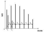
- FIG. 3 is a diagram showing frequency spectra of a first optical comb laser and a second optical comb laser in a dual comb.
- f CEO1 is an example of the first CEO frequency and is the carrier envelope offset frequency of the first optical comb laser.
- f CEO2 is an example of the second CEO frequency, and is the carrier envelope offset frequency of the second optical comb laser.
- f rep1 is the repetition frequency of the first optical comb laser.
- the frequency interval of the frequency spectrum of the interference light is ⁇ f rep , which is the difference between the repetition frequencies of the first optical comb laser and the second optical comb laser.
- X in the figure represents a value from 0 to the lowest frequency mode.
- F max represents the response frequency band of the detector. As shown in FIG. 4, if the frequency spectrum of the interference light falls within F max , detection of the dual comb signal is appropriate and can be used for various purposes such as ranging.
- a response frequency band of a detector may be interpreted as a frequency band that is detectable by the detector.
- ⁇ f rep may be the same as any fi.
- ⁇ f rep (f 1 +...+F n )/n.
- the minimum value of the response frequency band of the detector may be zero.
- the minimum value of the response frequency band of the detector may be a value other than zero.
- the lowest frequency mode is a result of interference between the i-th frequency mode f 1i of the first optical comb laser and the j-th frequency mode f 2j of the second optical comb laser.
- f rep 3 GHz
- ⁇ f rep 500 kHz
- i 65000
- i and j are values when the frequency of light is 195 THz.
- a detector with a high response frequency band exceeding 1 GHz has a problem of high cost, which becomes a barrier to industrial application.
- the present inventors conceived of a laser device that can control ⁇ f CEO so that dual comb measurements can be detected even with an inexpensive detector having a low response frequency band.
- the couplers 30, 31, 32, and 33 are optical elements that separate or combine light, respectively.
- the circulator 40 is an optical element that controls the traveling direction of light.
- the collimator 50 is an optical element that converts light into parallel light and emits it.
- a light condensing element such as a lens may be provided on the light output side of the collimator 50.
- the detection unit 70 includes detectors 71 and 72.
- the detectors 71 and 72 are optical elements that generate and output electrical signals by photoelectrically converting incident light.
- the signal level of the electrical signal corresponds to the intensity of incident light.
- the detectors 71 and 72 are, for example, photoelectric conversion elements such as photodiodes and phototransistors.
- the signal processing circuit 80 acquires information regarding the frequency spectrum of the dual comb signal based on the output of the detection unit 70.
- the dual comb signal is a frequency spectrum of interference light, and is, for example, the signal shown in FIG. 4. A specific example of information regarding the frequency spectrum will be described later.
- the signal processing circuit 80 (1) transmits information corresponding to the output of the detection unit 70 (that is, an electrical signal corresponding to the interference light) to a spectrum analyzer connected to the laser device 100 wirelessly or by wire; ) A frequency spectrum corresponding to the output of the detection unit 70, that is, corresponding to the interference light may be received from the spectrum analyzer.
- the signal processing circuit 80 calculates the distance to the target object 60 based on the output of the detection unit 70.
- the signal processing circuit 80 may calculate the distance to each part of the surface of the object 60 based on the output of the detection unit 70. Thereby, the signal processing circuit 80 can obtain information regarding the surface shape of the target object 60.
- the control circuit 90 changes ⁇ f CEO by controlling at least one of f CEO1 and f CEO2 based on the output of the detection unit 70.
- the specific processing of the control circuit 90 will be explained later.
- the signal processing circuit 80 and the control circuit 90 are each realized by, for example, an LSI (Large Scale Integration) that is an integrated circuit (IC). Note that the integrated circuit is not limited to an LSI, and may be a dedicated circuit or a general-purpose processor.
- signal processing circuit 80 and control circuit 90 may be microcontrollers.
- a microcontroller includes, for example, a nonvolatile memory in which a program is stored, a volatile memory that is a temporary storage area for executing the program, an input/output port, a processor that executes the program, and the like.
- the signal processing circuit 80 and the control circuit 90 may be a programmable FPGA (Field Programmable Gate Array) or a reconfigurable processor in which connections and settings of circuit cells within an LSI can be reconfigured.
- the functions performed by the signal processing circuit 80 and the control circuit 90 may be realized by software or hardware.
- the signal processing circuit 80 and the control circuit 90 may be realized by a common hardware configuration.
- optical fibers shown by broken lines in FIG. Specifically, couplers 30, 31, 32, and 33, a circulator 40, a collimator 50, and detectors 71 and 72 are arranged on the optical fiber path.
- the first optical comb laser 10 and the second optical comb laser 20 are connected to the ends of the optical fibers.
- the first optical comb laser beam 10L is divided into two parts, a light 10Lt and a light 10Lr, by the coupler 30.
- the light 10Lt is an optical comb laser beam for measurement, and is emitted toward the object 60.
- the light 10Lr is a reference optical comb laser beam.
- the light 10Lt passes through the circulator 40, is emitted from the collimator 50, and enters the object 60.
- the light 10Lt is then reflected by the object 60.
- the reflected light 10R from the object 60 enters the collimator 50, it is directed to the coupler 33 by the circulator 40. Further, the light 10Lr goes from the coupler 30 to the coupler 32.
- the second optical comb laser beam 20L is divided into two parts, a light 20Lr and a light 20Lt, by the coupler 31.
- the light 20Lt is an optical comb laser beam for measurement.
- the light 20Lr is a reference optical comb laser beam.
- the light 20Lr is combined with the light 10Lr at the coupler 32 and heads toward the detector 71. Further, the light 20Lt is combined with the reflected light 10R at the coupler 33 and heads toward the detector 72. When these lights interfere with each other in the detector 71 or 72, a beat is generated, and the light information is converted into an electrical signal. Electrical signals output from each of detectors 71 and 72 are input to signal processing circuit 80 .
- the signal processing circuit 80 uses the electric signal output from the detector 71 as a reference signal and the electric signal output from the detector 72 as a measurement signal to perform arithmetic processing and calculate the distance to the target object 60.
- the control circuit 90 controls the value of the carrier envelope offset frequency of at least one of the first optical comb laser 10 and the second optical comb laser 20 based on the electrical signal output from the detector 71, so that the difference frequency ⁇ f CEO change.
- the laser device 100 starts operating in response to a start signal from an input means (not shown).
- the input means is, for example, a physical button or a touch panel display that can be operated by the user.
- the input means is, for example, a physical button or a touch panel display that can be operated by the user.
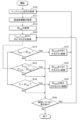
- There are multiple methods for controlling the ⁇ f CEO and each method will be explained in turn below.
- FIG. 6 is a flowchart showing the process of controlling ⁇ f CEO based on the lowest frequency mode in the frequency spectrum of the dual comb signal, among the operations of laser device 100 according to the present embodiment.
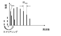
- FIG. 6 is to control so that X in FIG. 4 does not take a negative value. If X becomes a negative value, as shown in FIG. 7, the frequency spectrum will fold back around the zero value due to aliasing, making it impossible to properly detect the dual comb signal. Note that FIG. 7 is a diagram showing an example of an inappropriate frequency spectrum of a dual comb signal.
- Step S10 the signal processing circuit 80 acquires a dual comb signal detected by at least one of the detectors 71 and 72.
- the dual comb signal obtained here is time information of a pulse train as shown in FIG. Next, the process advances to step S11.
- Step S11 the signal processing circuit 80 acquires frequency information by converting the acquired time information.
- the frequency information acquired here is a frequency spectrum of interference light, for example, a frequency spectrum as shown in FIG. 4.
- the signal processing circuit 80 performs fast Fourier transform as an example of calculations used for conversion, but other methods may be used as long as time information can be converted into frequency information.
- the signal processing circuit 80 outputs the acquired frequency information to the control circuit 90.
- the process advances to step S12.
- Step S12 the control circuit 90 obtains ⁇ f rep , which is the difference in repetition frequency.
- ⁇ f rep the repetition frequency
- the control circuit 90 controls the repetition frequency f rep1 of the first optical comb laser 10 and the repetition frequency f rep2 of the second optical comb laser 20
- An example of controlling the repetition frequency is to control the cavity length of each of the first optical comb laser 10 and the second optical comb laser 20 by feedback control, but if the repetition frequency can be controlled, other It doesn't matter what method you use. Further, as long as information on ⁇ f rep can be obtained, a method other than the above may be used.
- the process advances to step S13.
- step S13 the control circuit 90 obtains first information regarding the lowest frequency mode of the frequency spectrum obtained in step S12. Specifically, the first information is the mode frequency f min of the lowest frequency mode. As an example, the control circuit 90 can detect f min by performing peak detection in the frequency spectrum, but other methods may be used as long as f min can be detected. Next, the process advances to step S14.
- step S14 the control circuit 90 determines whether f min is smaller than ⁇ f rep . In step S14, if f min is smaller than ⁇ f rep , that is, if Yes in step S14, the process advances to step S15. On the other hand, if f min is greater than or equal to ⁇ f rep in step S14, that is, if No in step S14, the control of ⁇ f CEO based on the lowest frequency mode ends. If No in step S14, ⁇ f CEO does not need to be changed.
- step S15 the control circuit 90 changes ⁇ f CEO by controlling at least one of f CEO1 of the first optical comb laser 10 and f CEO2 of the second optical comb laser 20.
- the control circuit 90 changes at least one of f CEO1 and f CEO2 by adjusting the output of the excitation source of the first optical comb laser 10 or the second optical comb laser 20, but does not change the value of f CEO1 or f CEO2 . If it can be changed, other methods such as control using an AOM (Acoustic Optic Modulator) may be used.
- AOM Acoustic Optic Modulator
- FIG. 7 shows an example where X shown in FIG. 4 takes a negative value and aliasing occurs.
- Two frequency modes represented by broken lines
- the lowest frequency mode is the third frequency mode from the left when no aliasing occurs, as shown in FIG.
- the control circuit 90 increases ⁇ f CEO by changing the value of f CEO1 or f CEO2 .
- the amount by which ⁇ f CEO is increased is adjusted as appropriate. Note that if ⁇ f CEO is made too large, a problem arises in that it exceeds the response frequency band. How to deal with this problem will be explained in detail later using FIGS. 8 and 9.
- the signal processing circuit 80 may acquire the dual comb signal detected by each of the detectors 71 and 72.
- the dual comb signals detected by each of detectors 71 and 72 are required.
- the position of the frequency spectrum may shift slightly due to the Doppler effect of light.
- the dual comb signals of each of the detectors 71 and 72 are acquired, and the processes of steps S11 to S15 are executed for each. Good too. The same applies to FIGS. 8, 10, and 12.
- FIG. 8 is a flowchart showing the process of controlling ⁇ f CEO based on the highest frequency mode in the frequency spectrum of the dual comb signal, among the operations of laser device 100 according to the present embodiment.
- FIG. 8 The process shown in FIG. 8 is to control the frequency spectrum so that it does not exceed the maximum value F max of the response frequency bands of the detectors 71 and 72 in FIG. 4 . If the frequency spectrum exceeds the maximum value F max of the response frequency bands of the detectors 71 and 72, the frequency spectrum will be aliased around F max due to aliasing, as shown in FIG. The signal cannot be detected properly.
- FIG. 9 is a diagram showing an example of an inappropriate frequency spectrum of a dual comb signal.
- the laser device 100 starts operating in response to a start signal from an input means (not shown). Steps S10, S11, and S12 are the same as the processing shown in FIG. 6, so their explanation will be omitted.
- step S23 the control circuit 90 obtains second information regarding the highest frequency mode of the frequency spectrum obtained in step S11.
- the second information is the mode frequency f max of the highest frequency mode.
- the control circuit 90 can detect f max by performing peak detection in the frequency spectrum, but other methods may be used as long as f max can be detected.
- the process advances to step S24.
- step S24 the control circuit 90 determines whether f max is greater than F max ⁇ f rep . In step S24, if f max is larger than F max ⁇ f rep , that is, if Yes in step S24, the process advances to step S25. On the other hand, if f max is less than or equal to F max ⁇ f rep in step S24, that is, if No in step S24, the control of ⁇ f CEO based on the highest frequency mode ends.
- step S25 the control circuit 90 changes ⁇ f CEO by controlling at least one of f CEO1 of the first optical comb laser 10 and f CEO2 of the second optical comb laser 20.
- the control circuit 90 changes at least one of f CEO1 and f CEO2 by adjusting the output of the excitation source of the first optical comb laser 10 or the second optical comb laser 20, but does not change the value of f CEO1 or f CEO2 . If it can be changed, other methods such as control using an AOM may be used.
- the process returns to step S10 and the above process is repeated. If No in step S24, ⁇ f CEO does not need to be changed.
- FIG. 9 shows an example in which aliasing occurs when the frequency spectrum exceeds the maximum value F max of the response frequency band.
- Five frequency modes represented by broken lines
- the highest frequency mode is the sixth frequency mode from the right when aliasing does not occur, as shown in FIG.
- the control circuit 90 reduces ⁇ f CEO by changing the value of f CEO1 or f CEO2 .
- the amount by which ⁇ f CEO is reduced is adjusted as appropriate. Note that if ⁇ f CEO is made too small, a problem arises in that X takes a negative value.
- the response to this problem is as described using FIGS. 6 and 7.
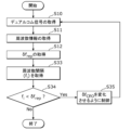
- FIG. 10 is a flowchart showing the process of controlling ⁇ f CEO based on the frequency interval in the frequency spectrum of the dual comb signal, among the operations of laser device 100 according to the present embodiment.
- the process shown in FIG. 10 is for controlling so that aliasing does not occur. If the frequency spectrum is folded back due to aliasing, the fact that a frequency interval smaller than ⁇ f rep occurs in the frequency spectrum is utilized, as shown in FIG.
- frequency intervals between adjacent frequency modes are represented by f 1 to f 8 . Due to the occurrence of aliasing, f 1 , f 2 , f 3 , and f 4 all become smaller than ⁇ f rep (Yes in step S34), so the control circuit 90 changes the value of f CEO1 or f CEO2 . This changes ⁇ f CEO . The amount by which ⁇ f CEO is changed is adjusted as appropriate.
- Step S43 the control circuit 90 acquires one of the lowest frequency mode mode frequency f min , the highest frequency mode mode frequency f max , and frequency interval f i for the frequency spectrum acquired in step S11.
- the control circuit 90 can detect f min , f max and f i by performing peak detection in the frequency spectrum, but if it can detect f min , f max and f i , other It doesn't matter what method you use.
- step S14 if f min is detected, the process proceeds to step S14, if f max is detected, the process proceeds to step S24, and if f i is detected, the process proceeds to step S34.
- the processing in each step S14, S24, and S34 is the same as the processing shown in FIGS. 6, 8, and 10. The same applies to steps S15, S25, and S35.
- the laser device 100 starts operating in response to a start signal from an input means (not shown).
- step S53 the control circuit 90 determines whether the accuracy ⁇ i calculated in step S52 is greater than the previous accuracy ⁇ i ⁇ 1 .
- the smaller the value of precision ⁇ i the better the precision, that is, the smaller the error between the distance measurement result and the actual distance.
- step S53 if ⁇ i is greater than ⁇ i ⁇ 1 , that is, if Yes in step S53, the process advances to step S54.
- step S53 if ⁇ i is smaller than ⁇ i ⁇ 1 in step S53, that is, if No in step S53, the control of ⁇ f CEO based on the accuracy of the distance ends. If No in step S53, ⁇ f CEO does not need to be changed.
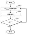
- FIG. 14 is a flowchart illustrating an example of a process for controlling ⁇ f CEO as a calibration before measurement among the operations of the laser device 100 according to the present embodiment.
- Step S62 it is determined whether to end distance measurement. Specifically, the signal processing circuit 80 or the control circuit 90 determines whether an end signal is input from an input means (not shown). If the measurement is to be completed in step S62, that is, in the case of Yes in step S62, the distance measurement is completed. On the other hand, if the measurement is to be continued in step S62, that is, if No in step S62, the process advances to step S61.
- FIG. 15 is a flowchart illustrating an example of the process of controlling ⁇ f CEO as feedback during measurement among the operations of laser device 100 according to the present embodiment.
- the processing executed by a specific processing unit may be executed by another processing unit.
- the order of the plurality of processes may be changed, or the plurality of processes may be executed in parallel.
- the processing described in the above embodiments may be realized by performing centralized processing using a single device (system), or by performing distributed processing using multiple devices. It's okay.
- the number of processors that execute the above program may be a single processor or a plurality of processors. That is, centralized processing or distributed processing may be performed.
- all or part of the components such as the signal processing circuit 80 and the control circuit 90 may be configured with dedicated hardware, or a software program suitable for each component may be executed. It may be realized by doing.
- Each component may be realized by a program execution unit such as a CPU (Central Processing Unit) or a processor reading and executing a software program recorded on a recording medium such as an HDD (Hard Disk Drive) or semiconductor memory. good.
- a program execution unit such as a CPU (Central Processing Unit) or a processor reading and executing a software program recorded on a recording medium such as an HDD (Hard Disk Drive) or semiconductor memory. good.
- components such as the signal processing circuit 80 and the control circuit 90 may be composed of one or more electronic circuits.
- Each of the one or more electronic circuits may be a general-purpose circuit or a dedicated circuit.
- the one or more electronic circuits may include, for example, a semiconductor device, an IC, or an LSI.
- An IC or LSI may be integrated into one chip or into multiple chips. Here, it is called an IC or an LSI, but the name changes depending on the degree of integration, and may be called a system LSI, VLSI (Very Large Scale Integration), or ULSI (Very Large Scale Integration).
- an FPGA that is programmed after the LSI is manufactured can also be used for the same purpose.
- general or specific aspects of the present disclosure may be implemented in a system, apparatus, method, integrated circuit, or computer program.
- the computer program may be implemented in a computer-readable non-transitory recording medium such as an optical disk, HDD, or semiconductor memory.
- the present invention may be realized by any combination of a system, an apparatus, a method, an integrated circuit, a computer program, and a recording medium.
- FIG. 16 is a diagram showing the processing flow of this modification.
- the laser device is: a first optical comb laser; a second optical comb laser; a detection section; comprising a control circuit;
- the control circuit causes the first optical comb laser to output light (1,p) in a p-th period
- the control circuit causes the second optical comb laser to output light (2, p) in a p-th period
- the detection unit receives light (3,p) based on the light (1,p) and the light (2,p),
- the f 1, n, p is the optical frequency of the n-th mode shown in the frequency spectrum characteristic (1, p) of the light (1, p)
- the f2 ,n,p is the optical frequency of the n-th mode shown in the frequency spectrum characteristic (2,p) of
- the light (1, p) may be a laser light output by the first optical comb laser 10 in the p-th period.
- the light (2, p) may be a laser light output by the second optical comb laser 20 in the p-th period.
- the light (3,p) may be light based on the light (1,p) and the light (2,p), and may be light that the detector 32 receives from the coupler 32.
- the pth period may start at time t p and end at time t (p+1) .
- the control circuit may cause the first optical comb laser to stop outputting the light (1,p) at a time that is after the time t p and before the time t (p+1 ). good.
- the control circuit may cause the second optical comb laser to stop outputting the light (2,p) at a time that is after the time t p and before the time t (p+1). good.
- the time at which the output of the light (2,p) ends may be after the time t p and before the time t (p+1) .
- the laser device according to the second item is the laser device according to the first item, the frequency spectrum characteristic (3, p) indicates f min ⁇ f rep ;
- the f min is a wavelength corresponding to the lowest frequency mode among the plurality of frequency modes shown in the frequency spectrum characteristic (3,p)
- the ⁇ f rep is the absolute value of the difference between two frequencies corresponding to two adjacent frequency modes in the frequency spectrum characteristic (3,p).
- the laser device is the laser device according to the first item, the frequency spectrum characteristic (3,p) indicates f max >(F max - ⁇ f rep );
- the f max is a wavelength corresponding to the highest frequency mode among the plurality of frequency modes shown in the frequency spectrum characteristic (3, p),
- the F max is the largest frequency included in a frequency band detectable by the detection unit,
- the ⁇ f rep is the absolute value of the difference between two frequencies corresponding to two adjacent frequency modes in the frequency spectrum characteristic (3,p).
- the present disclosure can be used in devices, systems, or methods that perform distance measurement or displacement measurement, and can be used, for example, in distance measurement sensors, displacement meters, shape inspection devices, and the like.
Landscapes
- Physics & Mathematics (AREA)
- Electromagnetism (AREA)
- Engineering & Computer Science (AREA)
- Plasma & Fusion (AREA)
- Optics & Photonics (AREA)
- Automation & Control Theory (AREA)
- General Physics & Mathematics (AREA)
- Lasers (AREA)
Abstract
Description
光コムレーザでは、2つのパラメータが重要である。1つはスペクトル間隔を表す「繰り返し周波数」(frep)である。もう1つはスペクトルを0まで外挿していった際の余りを表す「キャリアエンベロープオフセット周波数」(fCEO)である。これらのパラメータは、振動および温度などの外乱によって僅かに変化してしまう。これに対して、ペルチェ素子またはピエゾ素子などの変調機器を光コムレーザに組み込むことで、これらのパラメータを安定化させることができる。これにより、精密測定を実現することができる。
[光コムレーザ]
まず、図1および図2を参照して、光コムレーザの基本原理を簡単に説明する。
次に、図3および図4を参照して、デュアルコムの原理を簡単に説明する。
以下、本開示の実施の形態に係るレーザ装置の具体的な構成を説明する。
次に、δfCEOの制御方法の具体例について説明する。レーザ装置100は、図示しない入力手段からの開始信号により動作を開始する。入力手段は、例えば、ユーザが操作可能な物理ボタンまたはタッチパネルディスプレイなどである。δfCEOの制御方法としては、複数の方法があり、以下では、各方法について順に説明する。
まず、最も低い周波数モードを利用する例について、図6および図7を用いて説明する。
ステップS10では、信号処理回路80が、検出器71および72の少なくとも一方で検出したデュアルコム信号を取得する。ここで取得するデュアルコム信号は、図1に示すようなパルス列の時間情報である。次に、ステップS11に進む。
ステップS11では、信号処理回路80が、取得した時間情報を変換することで周波数情報を取得する。ここで取得する周波数情報は、干渉光の周波数スペクトルであり、例えば図4に示すような周波数スペクトルである。信号処理回路80は、変換に用いる演算の一例として高速フーリエ変換を行うが、時間情報を周波数情報に変換できれば他の手法を用いてもよい。信号処理回路80は、取得した周波数情報を制御回路90に出力する。次に、ステップS12に進む。
ステップS12では、制御回路90が、繰り返し周波数の差であるδfrepを取得する。例えば、制御回路90が第1光コムレーザ10の繰り返し周波数frep1および第2光コムレーザ20の繰り返し周波数frep2を制御している場合、制御回路90は、この制御情報に基づいてδfrep(=frep2-frep1)を取得する。繰り返し周波数の制御の一例として、第1光コムレーザ10および第2光コムレーザ20の各々の共振器長をフィードバック制御によって制御することが挙げられるが、繰り返し周波数を制御することができていれば他の方法でも構わない。また、δfrepの情報を取得できれば、上記とは別の方法を用いてもよい。次に、ステップS13に進む。
ステップS13では、制御回路90が、ステップS12で取得した周波数スペクトルの最も低い周波数モードに関する第1情報を取得する。具体的には、第1情報は、最も低い周波数モードのモード周波数fminである。一例として、制御回路90は、周波数スペクトルにおいてピーク検出を行うことで、fminを検出することができるが、fminを検出することができれば他の方法でも構わない。次に、ステップS14に進む。
ステップS14では、制御回路90が、fminがδfrepより小さいか否かを判断する。ステップS14において、fminがδfrepより小さい場合、すなわち、ステップS14おいてYesの場合は、ステップS15に進む。一方、ステップS14においてfminがδfrep以上である場合、すなわち、ステップS14においてNoの場合は、最も低い周波数モードに基づくδfCEOの制御は、終了する。ステップS14においてNoの場合は、δfCEOを変化させなくてもよい。
ステップS15では、制御回路90が、第1光コムレーザ10のfCEO1および第2光コムレーザ20のfCEO2の少なくとも一方を制御することで、δfCEOを変化させる。例えば、制御回路90は、第1光コムレーザ10または第2光コムレーザ20の励起源の出力を調整することで、fCEO1およびfCEO2の少なくとも一方を変更するが、fCEO1またはfCEO2の値を変更することができれば、例えばAOM(Acoustic Optic Modulator)を用いた制御などの他の方法でもよい。δfCEOを変更した後にステップS10に戻り、上記処理が繰り返される。
次に、最も高い周波数モードを利用する例について、図8および図9を用いて説明する。
ステップS23では、制御回路90は、ステップS11で取得した周波数スペクトルの最も高い周波数モードに関する第2情報を取得する。第2情報は、最も高い周波数モードのモード周波数fmaxである。一例として、制御回路90は、周波数スペクトルにおいてピーク検出を行うことで、fmaxを検出することができるが、fmaxを検出することができれば他の方法でも構わない。次に、ステップS24に進む。
ステップS24では、制御回路90が、fmaxがFmax-δfrepより大きい否かを判断する。ステップS24において、fmaxがFmax-δfrepより大きい場合、すなわち、ステップS24においてYesの場合は、ステップS25に進む。一方、ステップS24において、fmaxがFmax-δfrep以下である場合、すなわち、ステップS24においてNoの場合は、最も高い周波数モードに基づくδfCEOの制御は、終了する。
ステップS25では、制御回路90が、第1光コムレーザ10のfCEO1および第2光コムレーザ20のfCEO2の少なくとも一方を制御することで、δfCEOを変化させる。例えば、制御回路90は、第1光コムレーザ10または第2光コムレーザ20の励起源の出力を調整することで、fCEO1およびfCEO2の少なくとも一方を変更するが、fCEO1またはfCEO2の値を変更することができれば、例えばAOMを用いた制御などの他の方法でもよい。δfCEOを変更した後にステップS10に戻り、上記処理が繰り返される。ステップS24においてNoの場合は、δfCEOを変化させなくてもよい。
次に、周波数間隔を利用する例について、図10および図11を用いて説明する。
ステップS33では、制御回路90は、ステップS11で取得した周波数スペクトルの周波数間隔に関する第3情報を取得する。第3情報は、周波数スペクトルにおける全ての周波数モードにおける周波数間隔fiである。一例として、制御回路90は、周波数スペクトルにおいてピーク検出を行うことで、fiを検出することができるが、fiを検出することができれば他の方法でも構わない。次に、ステップS34に進む。なお、fiの添え字iは、周波数間隔の番号を表している。例えば、周波数モードの本数がN本の場合、iは、1以上N-1以下の値である。
ステップS34では、制御回路90が、i=1~N-1の各々について、fiがδfrepより小さい否かを判断する。ステップS34において、少なくとも1つのfiがδfrepより小さい場合、すなわち、ステップS34においてYesの場合は、ステップS35に進む。一方、ステップS34において、全てのfiがδfrepより小さくない場合、すなわち、ステップS34においてNoの場合は、周波数間隔に基づくδfCEOの制御は、終了する。ステップS34においてNoの場合は、δfCEOを変化させなくてもよい。
ステップS35では、制御回路90が、第1光コムレーザ10のfCEO1および第2光コムレーザ20のfCEO2の少なくとも一方を制御することで、δfCEOを変化させる。例えば、制御回路90は、第1光コムレーザ10または第2光コムレーザ20の励起源の出力を調整することで、fCEO1およびfCEO2の少なくとも一方を変更するが、fCEO1またはfCEO2の値を変更することができれば、例えばAOMを用いた制御などの他の方法でもよい。δfCEOを変更した後にステップS10に戻り、上記処理が繰り返される。図11は、図7と同様に、周波数スペクトルにエイリアシングが発生している例を示している。図11に示すように、隣り合う周波数モードの周波数間隔をf1からf8で表している。エイリアシングが発生することで、f1、f2、f3、f4はいずれも、δfrepより小さくなるので(ステップS34でYes)、制御回路90は、fCEO1またはfCEO2の値を変更することで、δfCEOを変化させる。δfCEOを変化させる量は、適宜調整される。
次に、最も低い周波数モード、最も高い周波数モードおよび周波数間隔を利用する例について、図12を用いて説明する。すなわち、制御回路90は、図6、図8および図10に示した各処理を組み合わせて行ってもよい。
ステップS43では、制御回路90は、ステップS11で取得した周波数スペクトルについて、最も低い周波数モードのモード周波数fmin、最も高い周波数モードのモード周波数fmaxおよび周波数間隔fiのいずれかを取得する。一例として、制御回路90は、周波数スペクトルにおいてピーク検出を行うことで、fmin、fmaxおよびfiを検出することができるが、fmin、fmaxおよびfiを検出することができれば他の方法でも構わない。次に、fminを検出した場合はステップS14に進み、fmaxを検出した場合はステップS24に進み、fiを検出した場合はステップS34に進む。各ステップS14、S24、S34での処理は、図6、図8および図10で示した処理と同じである。ステップS15、S25、S35についても同様である。
各ステップS14、S24、S34の各々においてNoである場合、すなわち、各ステップにおける条件を満たしていない場合、制御回路90は、検討していない条件があるか否かを判断する。検討していない条件がある場合、すなわち、ステップS46でYesの場合、ステップS43に戻り、検討していない条件に関するfmin、fmaxまたはfiを取得する。例えば、ステップS43でfminを取得し、fmin<δfrepを満たさなくなった場合(S14でNo)、再びステップS43に戻った場合には、fmaxまたはfiを取得する。制御回路90は、全ての条件についての検討が終了した場合、すなわち、ステップS46でNoの場合、δfCEOの制御は、終了する。
次に、対象物60までの距離の精度を利用する例について、図13を用いて説明する。
ステップS50では、信号処理回路80が、検出器71および72の各々で検出したデュアルコム信号を取得する。ここで取得するデュアルコム信号は、図1に示すようなパルス列の時間情報である。次に、ステップS51に進む。
ステップS51では、信号処理回路80が、検出器71から出力されるデュアルコム信号を基準信号とし、検出器72から出力されるデュアルコム信号を測定信号として演算処理を行うことで、対象物60までの距離を算出する。距離の算出方法の一例として、基準信号と測定信号とにおけるパルスのピーク差から距離を求めることが挙げられるが、フーリエ変換した後の位相情報を用いた距離算出などのように距離が求められれば他の方法でもよい。次に、ステップS52に進む。
ステップS52では、制御回路90が、ステップS51で算出した距離の精度σiを算出する。一例として、制御回路90は、数十回の測定結果の標準偏差を、精度σiとして算出するが、精度σiを求めることができれば他の方法でもよい。次に、ステップS53に進む。
ステップS53では、制御回路90が、ステップS52で算出した精度σiが一回前の精度σi-1より大きい否かを判断する。ここでは、精度σiの値が小さい程、精度が良い、すなわち、距離の測定結果と実際の距離との誤差が少ないことを意味する。ステップS53において、σiがσi-1より大きい場合、すなわち、ステップS53においてYesの場合は、ステップS54に進む。一方、ステップS53においてσiがσi-1より小さい場合、すなわち、ステップS53においてNoの場合は、距離の精度に基づくδfCEOの制御は、終了する。ステップS53においてNoの場合は、δfCEOを変化させなくてもよい。
ステップS54では、制御回路90が、第1光コムレーザ10のfCEO1および第2光コムレーザ20のfCEO2の少なくとも一方を制御することで、δfCEOを変化させる。例えば、制御回路90は、第1光コムレーザ10または第2光コムレーザ20の励起源の出力を調整することで、fCEO1およびfCEO2の少なくとも一方を変更するが、fCEO1またはfCEO2の値を変更することができれば、例えばAOMを用いた制御などの他の方法でもよい。δfCEOを変更した後にステップS50に戻り、上記処理が繰り返される。
次に、上述したδfCEOの制御を行うタイミングについて、図14および図15を用いて説明する。実際に距離を測定する際のδfCEOの制御は、測定前のキャリブレーションとして行う場合、および、随時フィードバックとして行う場合の2通りが考えられる。
図14は、本実施の形態に係るレーザ装置100の動作のうち、測定前のキャリブレーションとしてδfCEOを制御する処理の一例を示すフローチャートである。
ステップS60では、制御回路90は、実際に距離を測定する前に、デュアルコム信号の周波数スペクトルが検出器71および72の各々の応答周波数帯域の中に収まるように、δfCEOを制御する。具体的な制御方法は、図6、図8、図10、図12および図13で示した処理と同様のため、説明を省略する。次に、ステップS61に進む。図14に示される例では、これ以降、δfCEO制御の処理は行わない。
ステップS61では、検出器71および72の各々から出力される信号に基づいて、対象物60までの距離を測定する。具体的な距離の測定の方法は、図13のステップS51と同様のため、説明を省略する。
ステップS62では、距離の測定を終了するか否かを判断する。具体的には、信号処理回路80または制御回路90が、図示しない入力手段から終了信号の入力があるかどうかを判断する。ステップS62において測定を終了する場合、すなわち、ステップS62においてYesの場合は、距離の測定は終了する。一方、ステップS62において測定を継続する場合、すなわち、ステップS62においてNoの場合は、ステップS61に進む。
図15は、本実施の形態に係るレーザ装置100の動作のうち、測定中のフィードバックとしてδfCEOを制御する処理の一例を示すフローチャートである。
以上、1つまたは複数の態様に係るレーザ装置について、実施の形態に基づいて説明したが、本開示は、これらの実施の形態に限定されるものではない。本開示の主旨を逸脱しない限り、当業者が思いつく各種変形を本実施の形態に施したもの、および、異なる実施の形態における構成要素を組み合わせて構築される形態も、本開示の範囲内に含まれる。
本開示の実施の形態の変形例は下記に示すようなものであってもよい。
第1光コムレーザと、
第2光コムレーザと、
検出部と、
制御回路と、を備え、
前記制御回路は、前記第1光コムレーザに、第p期間に光(1,p)を出力させ、
前記制御回路は、前記第2光コムレーザに、第p期間に光(2,p)を出力させ、
前記検出部は、前記光(1,p)と前記光(2,p)に基づく光(3,p)を受け取り、
前記検出部は、前記光(3,p)に対応する第p情報を出力し、
f1,n,p=fCEO,1,p+n×frep,1であり、
f2,n,p=fCEO,2,p+n×frep,2であり、
前記f1,n,pは、前記光(1,p)の周波数スペクトル特性(1,p)において示された第nモードの光周波数であり、
前記f2,n,pは、前記光(2,p)の周波数スペクトル特性(2,p)において示された第nモードの光周波数であり、
前記fCEO,1,pは、前記周波数スペクトル特性(1,p)において示された第0モードに対応する周波数であり、
前記fCEO,2,pは、前記周波数スペクトル特性(2,p)において示された第0モードに対応する周波数であり、
前記frep,1と前記frep,2は異なり、
前記制御回路は、前記第p情報に基づく前記光(3,p)の周波数スペクトル特性(3,p)に基づいて、fCEO,1,(p+1)とfCEO,2,(p+1)を決定する。
前記周波数スペクトル特性(3,p)がfmin<δfrepを示し、
|fCEO,1,(p+1)-fCEO,2,(p+1)|>|fCEO,1,p-fCEO,2,p|であり、
前記fminは前記周波数スペクトル特性(3,p)において示された複数の周波数モードにおける最も低い周波数モードに対応する波長であり、
前記δfrepは前記周波数スペクトル特性(3,p)における隣接する2つの周波数モードに対応する2つの周波数の差の絶対値である。
前記周波数スペクトル特性(3,p)がfmax>(Fmax-δfrep)を示し、
|fCEO,1,(p+1)-fCEO,2,(p+1)|<|fCEO,1,p-fCEO,2,p|であり、
前記fmaxは前記周波数スペクトル特性(3,p)において示された複数の周波数モードにおける最も高い周波数モードに対応する波長であり、
前記Fmaxは前記検出部が検出可能な周波数帯域に含まれる最も大きい周波数であり、
前記δfrepは前記周波数スペクトル特性(3,p)における隣接する2つの周波数モードに対応する2つの周波数の差の絶対値である。
10L 第1光コムレーザ光
10Lr、10Lt、20Lr、20Lt 光
10R 反射光
20 第2光コムレーザ
20L 第2光コムレーザ光
30、31、32、33 カプラ
40 サーキュレータ
50 コリメータ
60 対象物
70 検出部
71、72 検出器
80 信号処理回路
90 制御回路
100 レーザ装置
Claims (8)
- 第1光コムレーザと、
前記第1光コムレーザとは繰り返し周波数が異なる第2光コムレーザと、
前記第1光コムレーザからの出力光と前記第2光コムレーザからの出力光とによる干渉光を検出する検出部と、
制御回路と、を備え、
前記制御回路は、前記第1光コムレーザのキャリアエンベロープオフセット周波数である第1CEO周波数と、前記第2光コムレーザのキャリアエンベロープオフセット周波数である第2CEO周波数との少なくとも一方を、前記検出部の出力に基づいて制御することで、前記第1CEO周波数と前記第2CEO周波数との差である差分周波数を変化させる、
レーザ装置。 - 前記制御回路は、前記検出部の出力に基づいて前記干渉光の周波数スペクトルの最も低い周波数モードに関する第1情報を取得し、取得した第1情報を用いて、前記差分周波数を大きくする、
請求項1に記載のレーザ装置。 - 前記制御回路は、前記検出部の出力に基づいて前記干渉光の周波数スペクトルの最も高い周波数モードに関する第2情報を取得し、取得した第2情報を用いて、前記差分周波数を小さくする、
請求項1に記載のレーザ装置。 - 前記制御回路は、前記検出部の出力に基づいて前記干渉光の周波数スペクトルの周波数間隔に関する第3情報を取得し、取得した第3情報を用いて、前記差分周波数を変化させる、
請求項1に記載のレーザ装置。 - 前記検出部は、前記第1光コムレーザからの出力光の、対象物による反射光と、前記第2光コムレーザからの出力光との干渉光を検出し、
前記レーザ装置は、前記検出部の出力に基づいて前記対象物までの距離を算出する信号処理回路を備える、
請求項1から4のいずれか1項に記載のレーザ装置。 - 前記制御回路は、前記信号処理回路が算出した距離の精度に基づいて前記差分周波数を変化させる、
請求項5に記載のレーザ装置。 - 前記制御回路は、前記距離の算出を行う前に前記差分周波数を変化させる、
請求項5に記載のレーザ装置。 - 前記制御回路は、前記距離の算出を行いながら前記差分周波数を変化させる、
請求項5に記載のレーザ装置。
Priority Applications (4)
| Application Number | Priority Date | Filing Date | Title |
|---|---|---|---|
| JP2024528652A JPWO2023243365A1 (ja) | 2022-06-14 | 2023-05-26 | |
| EP23823664.0A EP4542796A4 (en) | 2022-06-14 | 2023-05-26 | LASER DEVICE |
| CN202380043994.2A CN119301828A (zh) | 2022-06-14 | 2023-05-26 | 激光装置 |
| US18/964,752 US20250096516A1 (en) | 2022-06-14 | 2024-12-02 | Laser device |
Applications Claiming Priority (2)
| Application Number | Priority Date | Filing Date | Title |
|---|---|---|---|
| JP2022-095868 | 2022-06-14 | ||
| JP2022095868 | 2022-06-14 |
Related Child Applications (1)
| Application Number | Title | Priority Date | Filing Date |
|---|---|---|---|
| US18/964,752 Continuation US20250096516A1 (en) | 2022-06-14 | 2024-12-02 | Laser device |
Publications (1)
| Publication Number | Publication Date |
|---|---|
| WO2023243365A1 true WO2023243365A1 (ja) | 2023-12-21 |
Family
ID=89191184
Family Applications (1)
| Application Number | Title | Priority Date | Filing Date |
|---|---|---|---|
| PCT/JP2023/019655 Ceased WO2023243365A1 (ja) | 2022-06-14 | 2023-05-26 | レーザ装置 |
Country Status (5)
| Country | Link |
|---|---|
| US (1) | US20250096516A1 (ja) |
| EP (1) | EP4542796A4 (ja) |
| JP (1) | JPWO2023243365A1 (ja) |
| CN (1) | CN119301828A (ja) |
| WO (1) | WO2023243365A1 (ja) |
Families Citing this family (1)
| Publication number | Priority date | Publication date | Assignee | Title |
|---|---|---|---|---|
| JPWO2023163018A1 (ja) * | 2022-02-24 | 2023-08-31 |
Citations (8)
| Publication number | Priority date | Publication date | Assignee | Title |
|---|---|---|---|---|
| US5687261A (en) * | 1996-01-24 | 1997-11-11 | California Institute Of Technology | Fiber-optic delay-line stabilization of heterodyne optical signal generator and method using same |
| JP2009229918A (ja) * | 2008-03-24 | 2009-10-08 | Univ Of Electro-Communications | 広帯域離散スペクトル発生装置、及び、その周波数制御方法 |
| JP2013507005A (ja) * | 2009-10-02 | 2013-02-28 | イムラ アメリカ インコーポレイテッド | モード同期レーザによる光信号処理 |
| CN104316180A (zh) * | 2014-11-02 | 2015-01-28 | 华东师范大学 | 基于连续稳频激光的双光学频率梳光学成像方法 |
| JP5663499B2 (ja) | 2009-03-06 | 2015-02-04 | イムラ アメリカ インコーポレイテッド | デュアルパルスレーザシステムによる光走査及び撮像システム |
| US20170292875A1 (en) * | 2014-10-02 | 2017-10-12 | Gwangju Institute Of Science And Technology | Device for generating and detecting photo mixing-type continuous-wave terahertz using phase noise compensation method |
| JP6963322B2 (ja) | 2017-02-28 | 2021-11-10 | 国立大学法人電気通信大学 | 光コムの制御方法及び光コムの制御装置 |
| WO2021261240A1 (ja) * | 2020-06-26 | 2021-12-30 | パナソニックIpマネジメント株式会社 | デュアル光周波数コム発生装置および計測装置 |
Family Cites Families (5)
| Publication number | Priority date | Publication date | Assignee | Title |
|---|---|---|---|---|
| JP6269213B2 (ja) * | 2014-03-19 | 2018-01-31 | アイシン精機株式会社 | 距離測定装置及び距離測定方法 |
| US10753801B2 (en) * | 2016-12-07 | 2020-08-25 | UNIVERSITé LAVAL | Methods for performing dual-comb interferometry using a frequency offset relation |
| WO2020052785A1 (en) * | 2018-09-14 | 2020-03-19 | Max-Planck-Gesellschaft zur Förderung der Wissenschaften e. V. | Particle analysis method and apparatus for a spectrometry-based particle analysis |
| CA3093345C (en) * | 2019-09-16 | 2025-12-16 | The Regents Of The University Of Colorado, A Body Corporate | Systems and methods for dual comb spectroscopy |
| CN113295106B (zh) * | 2021-05-26 | 2022-07-15 | 清华大学 | 一种双光梳散斑干涉测量系统及测量方法 |
-
2023
- 2023-05-26 JP JP2024528652A patent/JPWO2023243365A1/ja active Pending
- 2023-05-26 EP EP23823664.0A patent/EP4542796A4/en active Pending
- 2023-05-26 CN CN202380043994.2A patent/CN119301828A/zh active Pending
- 2023-05-26 WO PCT/JP2023/019655 patent/WO2023243365A1/ja not_active Ceased
-
2024
- 2024-12-02 US US18/964,752 patent/US20250096516A1/en active Pending
Patent Citations (8)
| Publication number | Priority date | Publication date | Assignee | Title |
|---|---|---|---|---|
| US5687261A (en) * | 1996-01-24 | 1997-11-11 | California Institute Of Technology | Fiber-optic delay-line stabilization of heterodyne optical signal generator and method using same |
| JP2009229918A (ja) * | 2008-03-24 | 2009-10-08 | Univ Of Electro-Communications | 広帯域離散スペクトル発生装置、及び、その周波数制御方法 |
| JP5663499B2 (ja) | 2009-03-06 | 2015-02-04 | イムラ アメリカ インコーポレイテッド | デュアルパルスレーザシステムによる光走査及び撮像システム |
| JP2013507005A (ja) * | 2009-10-02 | 2013-02-28 | イムラ アメリカ インコーポレイテッド | モード同期レーザによる光信号処理 |
| US20170292875A1 (en) * | 2014-10-02 | 2017-10-12 | Gwangju Institute Of Science And Technology | Device for generating and detecting photo mixing-type continuous-wave terahertz using phase noise compensation method |
| CN104316180A (zh) * | 2014-11-02 | 2015-01-28 | 华东师范大学 | 基于连续稳频激光的双光学频率梳光学成像方法 |
| JP6963322B2 (ja) | 2017-02-28 | 2021-11-10 | 国立大学法人電気通信大学 | 光コムの制御方法及び光コムの制御装置 |
| WO2021261240A1 (ja) * | 2020-06-26 | 2021-12-30 | パナソニックIpマネジメント株式会社 | デュアル光周波数コム発生装置および計測装置 |
Non-Patent Citations (1)
| Title |
|---|
| See also references of EP4542796A4 |
Also Published As
| Publication number | Publication date |
|---|---|
| US20250096516A1 (en) | 2025-03-20 |
| EP4542796A4 (en) | 2025-09-17 |
| EP4542796A1 (en) | 2025-04-23 |
| JPWO2023243365A1 (ja) | 2023-12-21 |
| CN119301828A (zh) | 2025-01-10 |
Similar Documents
| Publication | Publication Date | Title |
|---|---|---|
| US8339611B2 (en) | Interferometric distance measurement with harmonic frequency comb generated beams | |
| EP4174569A1 (en) | Dual optical frequency comb generation device and measurement device | |
| JP6693783B2 (ja) | 距離測定装置およびその校正方法 | |
| JP5421013B2 (ja) | 位置決め装置及び位置決め方法 | |
| CN110274880A (zh) | 一种高精度空间分辨的光谱探测方法和系统 | |
| JP2000205814A (ja) | ヘテロダイン干渉計 | |
| US20250096516A1 (en) | Laser device | |
| JP7128516B2 (ja) | デュアルコム分光法における干渉信号の測定方法 | |
| JP2024017359A (ja) | 光学デバイスおよび分光装置 | |
| KR101398835B1 (ko) | 콤 생성 및 검출 장치를 이용한 실시간 분광형 간섭 측정 장치 및 측정 방법 | |
| CN109612601B (zh) | 一种电力设备温度和局部放电一体化检测系统及方法 | |
| US20250334679A1 (en) | Measurement device and measurement method | |
| RU2377497C1 (ru) | Устройство для измерения деформаций на основе квазираспределенных волоконно-оптических датчиков на брэгговских решетках | |
| JP2009544984A (ja) | 気体速度センサ | |
| JP6774192B2 (ja) | 距離測定装置および距離測定方法 | |
| JP2010261776A (ja) | 光波干渉計測装置 | |
| CN102066887B (zh) | 用于减少光的条纹干涉的方法 | |
| US12379494B2 (en) | Optical distance measurement device and machining device | |
| JP2012132711A (ja) | パルス間位相ズレ測定装置、オフセット周波数制御装置、パルス間位相ズレ測定方法、オフセット周波数制御方法 | |
| WO2024209789A1 (ja) | 距離測定装置 | |
| JP7610834B2 (ja) | 光周波数コムの周波数掃引量測定装置及び方法 | |
| WO2025150355A1 (ja) | 計測装置および計測方法 | |
| TW202240135A (zh) | 使用光輸出掃描系統和參考波長單元對光子設備進行的高準確度頻率測量 | |
| JPH06117810A (ja) | 外乱補正機能付きアブソリュ−ト測長器 | |
| JP6748986B2 (ja) | 群遅延時間差測定方法及び群遅延時間差測定装置 |
Legal Events
| Date | Code | Title | Description |
|---|---|---|---|
| 121 | Ep: the epo has been informed by wipo that ep was designated in this application |
Ref document number: 23823664 Country of ref document: EP Kind code of ref document: A1 |
|
| WWE | Wipo information: entry into national phase |
Ref document number: 202380043994.2 Country of ref document: CN |
|
| WWE | Wipo information: entry into national phase |
Ref document number: 2024528652 Country of ref document: JP |
|
| WWP | Wipo information: published in national office |
Ref document number: 202380043994.2 Country of ref document: CN |
|
| WWE | Wipo information: entry into national phase |
Ref document number: 2023823664 Country of ref document: EP |
|
| NENP | Non-entry into the national phase |
Ref country code: DE |
|
| ENP | Entry into the national phase |
Ref document number: 2023823664 Country of ref document: EP Effective date: 20250114 |
|
| WWP | Wipo information: published in national office |
Ref document number: 2023823664 Country of ref document: EP |