WO2023248453A1 - 積層造形用銅合金粉末、銅合金積層造形体および銅合金積層造形体の製造方法 - Google Patents
積層造形用銅合金粉末、銅合金積層造形体および銅合金積層造形体の製造方法 Download PDFInfo
- Publication number
- WO2023248453A1 WO2023248453A1 PCT/JP2022/025245 JP2022025245W WO2023248453A1 WO 2023248453 A1 WO2023248453 A1 WO 2023248453A1 JP 2022025245 W JP2022025245 W JP 2022025245W WO 2023248453 A1 WO2023248453 A1 WO 2023248453A1
- Authority
- WO
- WIPO (PCT)
- Prior art keywords
- copper alloy
- additive manufacturing
- powder
- weight
- less
- Prior art date
- Legal status (The legal status is an assumption and is not a legal conclusion. Google has not performed a legal analysis and makes no representation as to the accuracy of the status listed.)
- Ceased
Links
Images


Classifications
-
- B—PERFORMING OPERATIONS; TRANSPORTING
- B33—ADDITIVE MANUFACTURING TECHNOLOGY
- B33Y—ADDITIVE MANUFACTURING, i.e. MANUFACTURING OF THREE-DIMENSIONAL [3D] OBJECTS BY ADDITIVE DEPOSITION, ADDITIVE AGGLOMERATION OR ADDITIVE LAYERING, e.g. BY 3D PRINTING, STEREOLITHOGRAPHY OR SELECTIVE LASER SINTERING
- B33Y70/00—Materials specially adapted for additive manufacturing
-
- B—PERFORMING OPERATIONS; TRANSPORTING
- B22—CASTING; POWDER METALLURGY
- B22F—WORKING METALLIC POWDER; MANUFACTURE OF ARTICLES FROM METALLIC POWDER; MAKING METALLIC POWDER; APPARATUS OR DEVICES SPECIALLY ADAPTED FOR METALLIC POWDER
- B22F10/00—Additive manufacturing of workpieces or articles from metallic powder
- B22F10/20—Direct sintering or melting
- B22F10/28—Powder bed fusion, e.g. selective laser melting [SLM] or electron beam melting [EBM]
-
- B—PERFORMING OPERATIONS; TRANSPORTING
- B22—CASTING; POWDER METALLURGY
- B22F—WORKING METALLIC POWDER; MANUFACTURE OF ARTICLES FROM METALLIC POWDER; MAKING METALLIC POWDER; APPARATUS OR DEVICES SPECIALLY ADAPTED FOR METALLIC POWDER
- B22F10/00—Additive manufacturing of workpieces or articles from metallic powder
- B22F10/30—Process control
- B22F10/34—Process control of powder characteristics, e.g. density, oxidation or flowability
-
- B—PERFORMING OPERATIONS; TRANSPORTING
- B22—CASTING; POWDER METALLURGY
- B22F—WORKING METALLIC POWDER; MANUFACTURE OF ARTICLES FROM METALLIC POWDER; MAKING METALLIC POWDER; APPARATUS OR DEVICES SPECIALLY ADAPTED FOR METALLIC POWDER
- B22F10/00—Additive manufacturing of workpieces or articles from metallic powder
- B22F10/60—Treatment of workpieces or articles after build-up
- B22F10/64—Treatment of workpieces or articles after build-up by thermal means
-
- B—PERFORMING OPERATIONS; TRANSPORTING
- B33—ADDITIVE MANUFACTURING TECHNOLOGY
- B33Y—ADDITIVE MANUFACTURING, i.e. MANUFACTURING OF THREE-DIMENSIONAL [3D] OBJECTS BY ADDITIVE DEPOSITION, ADDITIVE AGGLOMERATION OR ADDITIVE LAYERING, e.g. BY 3D PRINTING, STEREOLITHOGRAPHY OR SELECTIVE LASER SINTERING
- B33Y40/00—Auxiliary operations or equipment, e.g. for material handling
- B33Y40/20—Post-treatment, e.g. curing, coating or polishing
-
- B—PERFORMING OPERATIONS; TRANSPORTING
- B33—ADDITIVE MANUFACTURING TECHNOLOGY
- B33Y—ADDITIVE MANUFACTURING, i.e. MANUFACTURING OF THREE-DIMENSIONAL [3D] OBJECTS BY ADDITIVE DEPOSITION, ADDITIVE AGGLOMERATION OR ADDITIVE LAYERING, e.g. BY 3D PRINTING, STEREOLITHOGRAPHY OR SELECTIVE LASER SINTERING
- B33Y80/00—Products made by additive manufacturing
-
- C—CHEMISTRY; METALLURGY
- C22—METALLURGY; FERROUS OR NON-FERROUS ALLOYS; TREATMENT OF ALLOYS OR NON-FERROUS METALS
- C22C—ALLOYS
- C22C1/00—Making non-ferrous alloys
- C22C1/04—Making non-ferrous alloys by powder metallurgy
-
- C—CHEMISTRY; METALLURGY
- C22—METALLURGY; FERROUS OR NON-FERROUS ALLOYS; TREATMENT OF ALLOYS OR NON-FERROUS METALS
- C22C—ALLOYS
- C22C1/00—Making non-ferrous alloys
- C22C1/04—Making non-ferrous alloys by powder metallurgy
- C22C1/0425—Copper-based alloys
-
- C—CHEMISTRY; METALLURGY
- C22—METALLURGY; FERROUS OR NON-FERROUS ALLOYS; TREATMENT OF ALLOYS OR NON-FERROUS METALS
- C22C—ALLOYS
- C22C1/00—Making non-ferrous alloys
- C22C1/10—Alloys containing non-metals
-
- C—CHEMISTRY; METALLURGY
- C22—METALLURGY; FERROUS OR NON-FERROUS ALLOYS; TREATMENT OF ALLOYS OR NON-FERROUS METALS
- C22C—ALLOYS
- C22C9/00—Alloys based on copper
- C22C9/06—Alloys based on copper with nickel or cobalt as the next major constituent
-
- C—CHEMISTRY; METALLURGY
- C22—METALLURGY; FERROUS OR NON-FERROUS ALLOYS; TREATMENT OF ALLOYS OR NON-FERROUS METALS
- C22F—CHANGING THE PHYSICAL STRUCTURE OF NON-FERROUS METALS AND NON-FERROUS ALLOYS
- C22F1/00—Changing the physical structure of non-ferrous metals or alloys by heat treatment or by hot or cold working
- C22F1/08—Changing the physical structure of non-ferrous metals or alloys by heat treatment or by hot or cold working of copper or alloys based thereon
-
- B—PERFORMING OPERATIONS; TRANSPORTING
- B22—CASTING; POWDER METALLURGY
- B22F—WORKING METALLIC POWDER; MANUFACTURE OF ARTICLES FROM METALLIC POWDER; MAKING METALLIC POWDER; APPARATUS OR DEVICES SPECIALLY ADAPTED FOR METALLIC POWDER
- B22F1/00—Metallic powder; Treatment of metallic powder, e.g. to facilitate working or to improve properties
-
- B—PERFORMING OPERATIONS; TRANSPORTING
- B22—CASTING; POWDER METALLURGY
- B22F—WORKING METALLIC POWDER; MANUFACTURE OF ARTICLES FROM METALLIC POWDER; MAKING METALLIC POWDER; APPARATUS OR DEVICES SPECIALLY ADAPTED FOR METALLIC POWDER
- B22F1/00—Metallic powder; Treatment of metallic powder, e.g. to facilitate working or to improve properties
- B22F1/05—Metallic powder characterised by the size or surface area of the particles
-
- B—PERFORMING OPERATIONS; TRANSPORTING
- B22—CASTING; POWDER METALLURGY
- B22F—WORKING METALLIC POWDER; MANUFACTURE OF ARTICLES FROM METALLIC POWDER; MAKING METALLIC POWDER; APPARATUS OR DEVICES SPECIALLY ADAPTED FOR METALLIC POWDER
- B22F2301/00—Metallic composition of the powder or its coating
- B22F2301/10—Copper
-
- B—PERFORMING OPERATIONS; TRANSPORTING
- B33—ADDITIVE MANUFACTURING TECHNOLOGY
- B33Y—ADDITIVE MANUFACTURING, i.e. MANUFACTURING OF THREE-DIMENSIONAL [3D] OBJECTS BY ADDITIVE DEPOSITION, ADDITIVE AGGLOMERATION OR ADDITIVE LAYERING, e.g. BY 3D PRINTING, STEREOLITHOGRAPHY OR SELECTIVE LASER SINTERING
- B33Y10/00—Processes of additive manufacturing
-
- Y—GENERAL TAGGING OF NEW TECHNOLOGICAL DEVELOPMENTS; GENERAL TAGGING OF CROSS-SECTIONAL TECHNOLOGIES SPANNING OVER SEVERAL SECTIONS OF THE IPC; TECHNICAL SUBJECTS COVERED BY FORMER USPC CROSS-REFERENCE ART COLLECTIONS [XRACs] AND DIGESTS
- Y02—TECHNOLOGIES OR APPLICATIONS FOR MITIGATION OR ADAPTATION AGAINST CLIMATE CHANGE
- Y02P—CLIMATE CHANGE MITIGATION TECHNOLOGIES IN THE PRODUCTION OR PROCESSING OF GOODS
- Y02P10/00—Technologies related to metal processing
- Y02P10/25—Process efficiency
Definitions
- the present invention relates to a copper alloy powder for layered manufacturing, a copper alloy layered object, and a method for producing a copper alloy layered object.
- Patent Document 1 discloses a copper-based alloy powder for additive manufacturing that contains nickel and silicon elements in copper.
- An object of the present invention is to provide a technology that solves the above problems.
- the copper alloy powder for additive manufacturing according to the present invention A copper alloy powder for additive manufacturing used for forming a additively manufactured object by an additive manufacturing method, Contains nickel and silicon, with the remainder consisting of copper and unavoidable impurities, A value obtained by dividing the nickel content (wt%) by the silicon content (wt%) is 3.3 or more and 7.2 or less.
- the copper alloy layered product according to the present invention has the following features: A copper alloy additively manufactured body produced by additively manufacturing using an additively manufacturing apparatus using the above-mentioned copper alloy powder for additively manufacturing, The value obtained by dividing the nickel content (wt%) by the silicon content (wt%) is 3.3 or more and 7.2 or less.
- the method for manufacturing a copper alloy layered product according to the present invention includes: An additive manufacturing step of additively manufacturing a copper alloy additive-molded body using an additive manufacturing device using the copper alloy powder for additive manufacturing; an aging treatment step of holding the copper alloy layered product at a temperature of 450° C. or higher and 550° C. or lower; including.
- a high-strength copper alloy laminate can be manufactured by efficiently producing a Corson alloy of nickel and silicon.
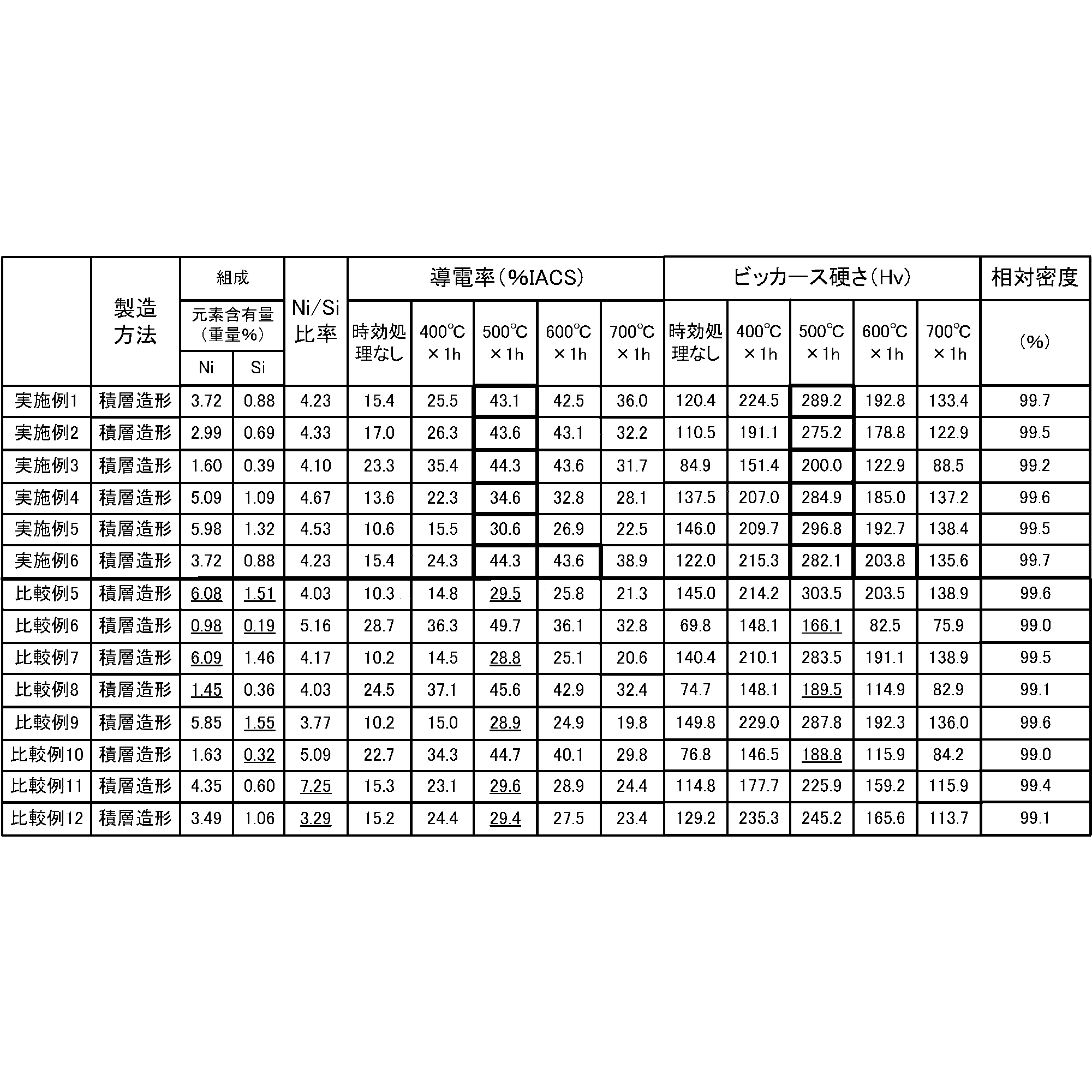
- FIG. 2 is a diagram showing the characteristics of the copper alloy laminate-molded bodies of Examples 1 to 6 and Comparative Examples 5 to 12.
- FIG. 3 is a diagram showing changes in characteristics of copper alloy laminate-molded bodies due to aging treatment in Examples 1 to 6.
- FIG. 3 is a diagram showing the characteristics of the copper alloy laminate-molded bodies of Examples 10 to 19.
- FIG. 3 is a diagram showing changes in characteristics of copper alloy laminate-molded bodies due to aging treatment in Examples 10 to 19.
- FIG. 3 is a diagram showing the characteristics of copper alloy laminate-molded bodies of Examples 1 to 6 and 10 to 19, Comparative Examples 21 to 34, and Comparative Examples 41 to 54.
- the manufacturing method of the copper alloy powder for additive manufacturing of this embodiment is not particularly limited, but there are methods such as gas atomization method, water atomization method, centrifugal atomization method, plasma atomization method, plasma rotating electrode method, etc., in which powder particles are rapidly cooled from a molten state. A solidified method is preferred. From the point of view of mass production, gas atomization is particularly preferred.
- the manufactured powder can be classified by a known classification method under predetermined classification conditions, and can be adjusted to a copper alloy powder for additive manufacturing with an appropriate particle size.
- an air classifier can be suitably used as a classification device for carrying out the classification.
- the nickel content is preferably 1.5% by weight or more. If it is less than 1.5% by weight, the amount of precipitation during aging treatment will be insufficient, and the effect of improving strength will not be sufficiently obtained.
- the solid solubility limit of Ni2Si which is one of the nickel-silicon intermetallic compounds in the Corson alloy, is said to be approximately 4.2% by weight for nickel and 1.0% by weight for silicon.
- the nickel-silicon intermetallic compound exceeding the solid solubility limit can be contained in the copper matrix without precipitation.
- the process involves melting and rapid solidification using a laser or electron beam, so it is possible to build without precipitating nickel-silicon intermetallic compounds exceeding the solid solubility limit. body can be created.
- the nickel content exceeds 6.0% by weight, the effect of further improving mechanical strength can be obtained, but this results in a significant decrease in electrical conductivity. Therefore, the nickel content is preferably 6.0% by weight or less.
- Silicon is a major element that forms and precipitates a nickel-silicon intermetallic compound together with nickel, contributing to improving the strength of copper alloys. If the content is less than 0.35% by weight, the amount of precipitation during aging treatment will be insufficient, and the effect of improving strength will not be sufficiently obtained. Further, if the amount exceeds 1.5% by weight, the conductivity will be significantly lowered and coarse precipitates will be formed, resulting in a decrease in strength, so it is preferably within the range of this embodiment.
- Nickel and silicon are the main elements that form nickel-silicon intermetallic compounds and contribute to improving electrical conductivity and strength. However, in order to improve both electrical conductivity and strength, it is necessary to contain nickel and silicon in an efficient ratio within their respective content ranges to form a nickel-silicon intermetallic compound. It is.
- the ratio the value obtained by dividing the nickel content (wt%) by the silicon content (wt%) is preferably in the range of 3.3 or more and 7.2 or less. If this ratio exceeds 7.2 and nickel is contained in excess of silicon, the excess nickel will be dissolved in the copper matrix, resulting in a significant decrease in electrical conductivity. On the other hand, if the ratio is less than 3.3 and silicon is contained in excess of nickel, the excess silicon will dissolve in the copper matrix, resulting in a significant decrease in electrical conductivity.
- the powder used for additive manufacturing is compatible with each process of additive manufacturing, such as the feeding process from a hopper onto the modeling stage, the process of forming a uniformly spread powder layer with a constant thickness, and the process of melting and solidification. are required to do so. Therefore, the following conditions are required.
- the conditions are: particle size adjusted within an appropriate range, apparent density within an appropriate range, and powder fluidity that allows it to be fed from the supply hopper and form an appropriate powder layer. It is.
- the 50% particle size of the copper alloy powder for additive manufacturing refers to the 50% particle size of the particle size distribution when measured by laser diffraction, and is preferably in the range of 3 ⁇ m or more and 200 ⁇ m or less.
- the 50% particle size is less than 3 ⁇ m, the powder has no fluidity, and a powder layer cannot be formed even in an additive manufacturing apparatus using a laser powder bed melting method.
- laser is irradiated to powder with a 50% particle size of less than 3 ⁇ m, the powder and droplets generated by melting the powder scatter, making it unsuitable for additive manufacturing.
- the 50% particle size is larger than 100 ⁇ m when additive manufacturing is performed using laser powder bed melting method, and when the 50% particle size is larger than 200 ⁇ m when additive manufacturing is performed using electron beam powder bed melting method, the surface of the powder layer The powder layer becomes rough and cannot form an appropriate powder layer for modeling. Furthermore, the melt pool generated in the powder layer during electron beam irradiation does not reach the solidified layer immediately below, resulting in insufficient melting and solidification, making it unsuitable for additive manufacturing.
- the 50% particle size is preferably 3 ⁇ m or more and 100 ⁇ m or less, more preferably 5 ⁇ m or more and 75 ⁇ m or less, and even more preferably 10 ⁇ m or more and 45 ⁇ m or less.
- the 50% particle size is preferably 10 ⁇ m or more and 200 ⁇ m or less, more preferably 25 ⁇ m or more and 150 ⁇ m or less, and even more preferably 45 ⁇ m or more and 105 ⁇ m or less.
- Copper alloy powder that can be additively manufactured using an additive manufacturing device has an apparent density (AD: Apparent Density) of 3 when measured using the JIS Z 2504 measurement method based on ISO 3923-1. .0g/cm3 or more is required.
- AD Apparent Density
- the apparent density is less than 3.0 g/cm 3 , the powder filling rate of the powder layer spread by squeegeeing decreases, making it impossible to form an appropriate powder layer.
- pores are generated in the shaped body, resulting in a decrease in the density of the shaped body.
- the apparent density of the copper alloy powder for layered manufacturing is more preferably 3.5 g/cm 3 or more.
- fluidity is a particularly important powder property.
- the most important powder characteristics are the powder supply from the supply hopper, the powder supply from the recoater, and the formation of a powder layer on the modeling stage, which are directly linked to the quality of the shaped object.
- the powder used in additive manufacturing requires sufficient squeegeeability, and for this purpose, the powder needs to have appropriate fluidity.
- the flow rate (FR) defined by JIS Z 2502 "Metal powder - Flow rate measurement method” based on ISO 4490 is used.
- the one-sided shear test method for powder specified in the Japan Powder Industry Technology Association standard (SAP15-13: 2013) "One-plane shear test method for powder” is recommended. It is effective to use the adhesion force of powder obtained by (hereinafter referred to as a shear test). Adhesion strength is measured in a shear test by measuring the shear stress that occurs when a powder layer formed by compacting the powder in the vertical direction is slid horizontally under pressure in the vertical direction. It can be determined from the fracture envelope of the body layer.
- the shear test can be measured using, for example, a powder rheometer FT4 manufactured by Freeman Technology.
- copper alloy powder for additive manufacturing if its adhesive force is 0.600 kPa or less, it can be judged that it has sufficient fluidity to spread a uniform powder layer and has good squeegeeability. can. As a result, a high-density and homogeneous laminate-molded body can be obtained.
- the adhesion force is greater than 0.600 kPa, the fluidity of the copper alloy powder for additive manufacturing is insufficient, the squeezing property is poor, and an appropriate powder layer cannot be formed. Therefore, in the copper alloy powder for additive manufacturing, it is desirable that the adhesion force of the copper alloy powder determined from the fracture envelope obtained by the shear test is 0.600 kPa or less.
- ⁇ Manufacture of a copper alloy layered object using the copper alloy powder for layered manufacturing of this embodiment Various known metal additive manufacturing techniques can be used as a method for manufacturing the copper alloy additive manufacturing body.
- metal powder is spread on a modeling stage using a blade or roller to form a powder layer, and a laser or electron beam is irradiated at a predetermined position on the formed powder layer to sinter the metal powder.
- a laser or electron beam is irradiated at a predetermined position on the formed powder layer to sinter the metal powder.
- the main parameters are adjusted using energy density, which is an index that summarizes the main parameters.
- the energy density is preferably 150 J/mm 3 or more and 450 J/mm 3 or less.
- the powder layer will be unfused or poorly fused, resulting in defects such as voids in the shaped body.
- the energy density exceeds 450 J/mm 3 , sputtering occurs and the surface of the powder layer becomes unstable, resulting in defects such as voids in the shaped body.
- the preheating temperature is preferably set at 300°C or more and 800°C or less.
- the metal additive manufacturing technology using the powder bed melting method is illustrated here, the general additive manufacturing method for producing a additively manufactured object using the copper alloy powder for additive manufacturing of this embodiment is limited to this.
- an additive manufacturing method using a directed energy deposition method may be adopted.
- the aging treatment step is an essential step in order to obtain the high strength and high conductivity properties of this embodiment.
- the aging treatment can be carried out by heating the laminate to a predetermined temperature and holding it for a predetermined time.
- the aging treatment is preferably carried out in a reducing atmosphere or inert gas in a vacuum.
- the effect of aging treatment is determined by the combination of aging treatment temperature and aging treatment time, so it is important to set appropriate conditions in balance with the desired characteristics and efficiency.
- the aging treatment temperature is preferably 450°C or more and 550°C or less. More preferably, the temperature is 450°C or higher and 500°C or lower. When it is desired to particularly improve mechanical strength, the temperature is preferably 500°C. If particularly high conductivity is desired, the temperature can be set at 550°C. When the aging treatment temperature is 450° C. or higher, the aging treatment time is preferably set to 0.5 hours or more and 3 hours or less.
- the aging treatment time is less than the set time, the precipitation of nickel and silicon will be insufficient. Furthermore, if the aging treatment time exceeds the set time, the nickel-silicon intermetallic compound precipitated due to overaging becomes coarse, resulting in a decrease in hardness. If the aging treatment temperature is less than 450° C., it is not practical because it takes a long time to obtain the aging effect. Further, if the aging treatment temperature exceeds 550° C., over-aging occurs, and the precipitated phase of the nickel-silicon intermetallic compound becomes coarse, resulting in a decrease in strength.
- nickel-silicon intermetallic compounds are precipitated due to thermal strain introduced by the rapid melting and solidification process that is a feature of additive manufacturing. It becomes easier to do. Therefore, it is possible to sufficiently improve the electrical conductivity and mechanical strength even with an aging treatment temperature of 450° C. or more and 550° C. or less and an aging treatment time of about 1 hour.
- the Vickers hardness of the copper alloy laminate-molded article of this embodiment is measured by a method based on JIS Z 2244: Vickers hardness test-test method. Vickers hardness can be measured using, for example, a microhardness tester HMV-G21-DT manufactured by Shimadzu Corporation.
- the copper alloy laminate-molded article of this embodiment has an electrical conductivity of 30% IACS or more.
- the conductivity can be measured using, for example, an eddy current conductivity meter.
- Examples of the eddy current conductivity meter include the high performance eddy current conductivity meter Sigma Check manufactured by Nippon Matek Co., Ltd.
- IACS International Annealed Copper Standard
- the electrical conductivity can be adjusted by aging treatment, and is preferably adjusted appropriately depending on the desired Vickers hardness.
- the conductivity is preferably 35% IACS or more, more preferably 40% IACS or more.
- the copper alloy additively manufactured body produced by additive manufacturing using the additively manufactured copper alloy powder of the present embodiment by the additive manufacturing apparatus has high electrical conductivity, it can be used as a copper alloy additively manufactured body having high thermal conductivity. is also available.
- the present embodiment contains nickel and silicon, and one or more selected from other metal elements such as iron, silver, magnesium, manganese, tin, and zinc, with the remainder being copper and unavoidable impurities.
- a copper alloy powder for additive manufacturing consisting of the following will be described, and a copper alloy additive-molded body produced by additive manufacturing using the copper alloy powder for additive manufacturing.
- the copper alloy powder for additive manufacturing of this embodiment may contain one or more elements selected from iron, silver, magnesium, manganese, tin, and zinc as necessary. It can be included. The effects of containing these metal elements will be explained below.
- Iron has the effect of refining the structure of the copper alloy layered product of this embodiment and improving its strength. Further, by combining with silicon, an iron-silicon compound is formed. Therefore, mechanical properties and heat resistance can be improved without significantly reducing conductivity. Iron is preferably adjusted to a range of 0.01% to 1.00% by weight, more preferably 0.05% to 0.30% by weight.
- silver has the effect of increasing the electrical conductivity of the copper alloy laminate manufactured body of this embodiment and the effect of increasing the strength by solid solution strengthening. It also has the effect of increasing the chemical potential of nickel, increasing the repulsive interaction between elements, and promoting the precipitation of nickel-silicon intermetallic compounds.
- silver content exceeds 1.0% by weight, the ratio of silver increases, but increasing the amount of silver does not have a significant effect on the properties, and the excessive content of expensive silver increases costs. invite. Therefore, silver is preferably adjusted to a range of 0.01% by weight or more and 1.00% by weight or less, and more preferably adjusted to a range of 0.05% by weight or more and 0.30% by weight or less.
- Magnesium is preferably adjusted to a range of 0.01% by weight or more and 1.00% by weight or less, and more preferably adjusted to a range of 0.05% by weight or more and 0.35% by weight or less.
- ⁇ Containing manganese acts as a deoxidizing agent and can suppress the effects of oxygen that degrades quality by combining with it to form a compound. It also has the effect of making the structure finer and improving its strength.
- Manganese is preferably adjusted to a range of 0.01% to 1.00% by weight, more preferably 0.05% to 0.20% by weight.
- tin is preferably adjusted to a range of 0.01% by weight or more and 1.00% by weight or less, and more preferably adjusted to a range of 0.05% by weight or more and 0.50% by weight or less.
- Zinc is preferably adjusted to a range of 0.01% by weight or more and 1.00% by weight or less, and more preferably adjusted to a range of 0.05% by weight or more and 0.50% by weight or less.
- the total content of these elements is preferably 1.0% by weight or less.
- Corson alloy has high strength and high conductivity by applying strain through plastic working such as rolling or forging, that is, strong working, after solution treatment, and by applying heat treatment to precipitate fine nickel-silicon intermetallic compounds. It is known that excellent properties such as high thermal conductivity and high thermal conductivity can be obtained.
- a method for manufacturing these Corson alloys for example, a method is known in which a cast Corson alloy ingot is hot forged, then subjected to solution heat treatment, and then subjected to aging treatment. Furthermore, a method is known in which a cast Corson alloy ingot is subjected to blooming and hot finishing by forging or rolling, then rapidly cooled after solution treatment, and then subjected to mechanical processing and aging treatment. Furthermore, a method is known in which a cast Corson alloy ingot is hot-worked, then annealed, and then cooled and then subjected to aging treatment. Furthermore, a method is known in which a cast Corson alloy ingot is hot forged, subjected to cold plastic working after solution treatment, and then subjected to aging treatment.
- a high-strength copper alloy layered product can be manufactured by efficiently producing a Corson alloy of nickel and silicon.
- copper alloy additive manufacturing with further improved electrical conductivity and strength by further containing other metal elements such as iron, silver, magnesium, manganese, tin, and zinc in addition to nickel and silicon. body can be manufactured.
- additive manufacturing is used for manufacturing a copper alloy additive manufacturing body that has both high electrical conductivity, high thermal conductivity, and excellent mechanical strength without requiring solution treatment and plastic working processes. It is possible to provide a copper alloy powder for use in the present invention, and a copper alloy layered product formed by layered manufacturing.
- copper alloy molds for die casting and plastic molding, electrodes for resistance welding, etc. can be made with high electrical conductivity, high thermal conductivity, and high strength. However, it can be manufactured with high efficiency without solution treatment and plastic working processes.
- Example of copper alloy powder for additive manufacturing containing nickel and silicon Copper alloy additive manufacturing in which a copper alloy powder for additive manufacturing containing nickel and silicon is produced by changing the content and content ratio of nickel and silicon, and then additive manufacturing is performed using the copper alloy powder for additive manufacturing. manufactured bodies and measured their properties.
- a copper alloy powder for additive manufacturing of a copper alloy containing nickel and silicon shown in Table 1 was produced by a gas atomization method.
- the obtained copper alloy powder for additive manufacturing was classified into a particle size of 10 ⁇ m or more and 45 ⁇ m or less for laser powder bed melting, and a particle size of 45 ⁇ m or more and 105 ⁇ m or less for electron beam powder bed melting. .
- the content of component elements in the obtained copper alloy powder for additive manufacturing was measured by ICP emission spectroscopy. Further, the apparent density (AD) (g/cm 3 ) of the obtained copper alloy powder for additive manufacturing was measured according to JIS Z 2504. Further, the flow rate (FR) (sec/50 g) of the obtained copper alloy powder for additive manufacturing was measured according to JIS Z 2502. Further, the 50% particle size (D50) ( ⁇ m) was measured by laser diffraction method (Microtrac MT3300: manufactured by Microtrac Bell Co., Ltd.).
- a shear test was conducted using a powder rheometer FT4 (manufactured by Freeman Technology), and the adhesion force (kPa) of the obtained copper alloy powder for additive manufacturing was measured.
- the squeezing property of the obtained copper alloy powder for additive manufacturing was measured by actually spreading the powder to be used for the modeling test on the modeling stage of a 3D additive manufacturing machine (powder sintering additive manufacturing/laser method or electron beam method). Evaluation was made by forming a layer.
- Table 1 shows the measurement results of each characteristic of the copper alloy powders for additive manufacturing of Examples 1 to 6 and Comparative Examples 1 to 12. In Table 1, the underlined property values indicate values that do not satisfy the condition range (expected value) as a copper alloy powder for additive manufacturing.
- the copper alloy powders of Comparative Examples 1 to 4 had poor squeezing properties, so normal additive manufacturing could not be performed.
- the powder could not be evenly spread and could not be shaped.
- the copper alloy powder of Comparative Example 1 satisfies the conditions for the content and ratio of nickel and silicon, and the 50% particle size (D50), but does not satisfy the conditions for the apparent density (AD) and adhesive force.
- the copper alloy powder of Comparative Example 2 satisfies the conditions for the content and ratio of nickel and silicon, but does not satisfy the conditions for the 50% particle size (D50), apparent density (AD), and adhesive force.
- the copper alloy powder of Comparative Example 3 satisfies the conditions for the content and ratio of nickel and silicon, the 50% particle size (D50), and the apparent density (AD), but does not satisfy the conditions for adhesive force.
- the powder layer was insufficiently filled and the density was low.
- the copper alloy powder of Comparative Example 4 satisfies the conditions for the content and ratio of nickel and silicon, the 50% particle size (D50), and the adhesive force, but does not satisfy the conditions for the apparent density (AD).
- the additive manufacturing was performed under the following conditions: a layer thickness of 25 ⁇ m or more and 50 ⁇ m or less, a laser output of 300 W or more and 700 W or less, a scanning speed of 900 mm/sec or more and 1500 mm/sec or less, and an energy density of 150 J/mm 3 or more and 450 J/mm 3 or less.
- a laminate model to be tested was manufactured using a 3D powder additive manufacturing machine (ArcamAB, EBM A2X) equipped with an electron beam.
- the additive manufacturing was performed under the conditions that the layer thickness was 50 ⁇ m or more and 100 ⁇ m or less, the electron beam voltage was 60 kV, and the preheating temperature was 300° C. or more and 700° C. or less.
- a cylindrical additive-molded body having a diameter of 14 mm and a height of 10 mm was manufactured using a 3D powder additive manufacturing machine.
- the electrical conductivity (%IACS) of the copper alloy additive manufactured bodies of Examples 1 to 6 and Comparative Examples 5 to 12 manufactured using a 3D powder additive manufacturing machine was measured using an eddy current conductivity meter (high performance eddy current conductivity Total Sigma Check: Made by Nippon Matek Co., Ltd.).
- the Vickers hardness (Hv) of the copper alloy laminate-molded body was measured using a microhardness tester (microhardness tester HMV-G21-DT: manufactured by Shimadzu Corporation).
- the prepared copper alloy laminate was subjected to aging treatment for 1 hour at temperatures set at 400°C, 500°C, 600°C, and 700°C in an inert atmosphere.
- the conductivity of the aged copper alloy laminate was measured using an eddy current conductivity meter.
- Vickers hardness was measured using a microhardness tester.
- Table 2 shows the evaluation results of various properties for the laminate bodies of Examples 1 to 6 and Comparative Examples 5 to 12 manufactured using a 3D powder additive manufacturing machine.
- the values of the properties surrounded by thick frames indicate values that satisfy the condition range as a copper alloy layered product.
- the underlined property values are values that do not satisfy the condition range as a copper alloy additively manufactured object even after aging treatment at 500°C, and values that do not satisfy the condition range as a copper alloy powder for additive manufacturing. show.
- Example 1 to 6 the content and ratio of nickel and silicon, and the properties of the copper alloy powder for additive manufacturing are within the required range, so that sufficient electrical conductivity (30% IACS or more) is achieved by the prescribed aging treatment. It was possible to fabricate a copper alloy laminate-molded body having both high strength and strength (Vickers hardness: 200 Hv or more).
- Comparative Example 5 the contents of nickel and silicon were excessive and outside the condition range, so although it exhibited high Vickers hardness, the conductivity was a low value.
- Comparative Example 6 the contents of nickel and silicon were too low and were out of the range of conditions, so although the conductivity was high, the Vickers hardness was low.
- Comparative Example 7 had an excessive nickel content, and Comparative Example 9 had an excessive silicon content, so although it exhibited high Vickers hardness, its conductivity was low.
- Comparative Example 8 the nickel content was too low, and in Comparative Example 10, the silicon content was too low, so although the conductivity was high, the Vickers hardness was low.
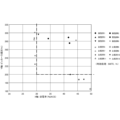
- Figure 1 is a diagram plotting the characteristics of Examples 1 to 6 and Comparative Examples 5 to 12, with the electrical conductivity (%IACS) at 500°C aging treatment taken on the X axis and the Vickers hardness (Hv) taken on the Y axis. be.
- %IACS electrical conductivity
- Hv Vickers hardness
- Figure 2 is a diagram plotting the characteristics of electrical conductivity (%IACS) or Vickers hardness (Hv) when the aging treatment temperature was changed from 400°C to 700°C in Examples 1 to 6. be.
- the temperature range of the aging treatment in Examples 1 to 6 is preferably 450 ° C. or higher and 550 ° C. or lower, preferably 550 ° C. if you want to increase the conductivity, and 500 ° C. if you want to increase the Vickers hardness.
- Copper alloy powder for additive manufacturing is manufactured by changing the content and content ratio of nickel and silicon and the content of other metal elements, and then copper is produced by additive manufacturing using the copper alloy powder for additive manufacturing. Alloy additively manufactured bodies were manufactured and their properties were measured.
- a copper alloy powder for additive manufacturing of a copper alloy containing nickel and silicon and other metal elements shown in Table 3 was produced by a gas atomization method.
- the obtained copper alloy powder for additive manufacturing was classified into a particle size of 10 ⁇ m or more and 45 ⁇ m or less for laser powder bed melting, and a particle size of 45 ⁇ m or more and 105 ⁇ m or less for electron beam powder bed melting. .
- the content of component elements in the obtained copper alloy powder for additive manufacturing was measured by ICP emission spectroscopy. Further, the apparent density (AD) (g/cm 3 ) of the obtained copper alloy powder for additive manufacturing was measured according to JIS Z 2504. Further, the flow rate (FR) (sec/50 g) of the obtained copper alloy powder for additive manufacturing was measured according to JIS Z 2502. Further, the 50% particle size (D50) ( ⁇ m) was measured by laser diffraction method (Microtrac MT3300: manufactured by Microtrac Bell Co., Ltd.).
- a shear test was conducted using a powder rheometer FT4 (manufactured by Freeman Technology), and the adhesion force (kPa) of the obtained copper alloy powder for additive manufacturing was measured.
- the squeezing property of the obtained copper alloy powder for additive manufacturing was measured by actually spreading the powder to be used for the modeling test on the modeling stage of a 3D additive manufacturing machine (powder sintering additive manufacturing/laser method or electron beam method). Evaluation was made by forming a layer.
- Table 3 shows the measurement results of each characteristic of the copper alloy powders for additive manufacturing of Examples 10 to 19.
- a laminate manufactured body for testing was produced using a 3D powder additive manufacturing machine (SLM Solutions GmbH, SLM280HL) equipped with a Yb fiber laser with a wavelength of 1064 nm. did.
- the additive manufacturing was performed under the following conditions: a layer thickness of 25 ⁇ m or more and 50 ⁇ m or less, a laser output of 300 W or more and 700 W or less, a scanning speed of 900 mm/sec or more and 1500 mm/sec or less, and an energy density of 150 J/mm 3 or more and 450 J/mm 3 or less.
- a laminate model to be tested was manufactured using a 3D powder additive manufacturing machine (ArcamAB, EBM A2X) equipped with an electron beam.
- the additive manufacturing was performed under the conditions that the layer thickness was 50 ⁇ m or more and 100 ⁇ m or less, the electron beam voltage was 60 kV, and the preheating temperature was 300° C. or more and 700° C. or less.
- a cylindrical additive-molded body having a diameter of 14 mm and a height of 10 mm was manufactured using a 3D powder additive manufacturing machine.
- the electrical conductivity (%IACS) of the copper alloy additive bodies of Examples 10 to 19 manufactured using a 3D powder additive manufacturing machine was measured using an eddy current conductivity meter (high performance eddy current conductivity meter Sigma Check: Nippon Matec) Co., Ltd.).
- the Vickers hardness (Hv) of the copper alloy laminate-molded body was measured using a microhardness tester (microhardness tester HMV-G21-DT: manufactured by Shimadzu Corporation).
- the prepared copper alloy laminate was subjected to aging treatment for 1 hour at temperatures set at 400°C, 500°C, 600°C, and 700°C in an inert atmosphere.
- the conductivity of the aged copper alloy laminate was measured using an eddy current conductivity meter.
- Vickers hardness was measured using a microhardness tester.
- Table 4 shows the evaluation results of various properties of the additively molded bodies of Examples 10 to 19 manufactured using the 3D powder additive manufacturing machine. In Table 4, the values of the properties surrounded by thick frames indicate values that satisfy the condition range as a copper alloy layered product.
- the content and ratio of nickel and silicon, and the properties of the copper alloy powder for additive manufacturing are within the required range, so that sufficient electrical conductivity (30% IACS or more) is achieved by the prescribed aging treatment. It was possible to fabricate a copper alloy laminate-molded body having both high strength and strength (Vickers hardness: 200 Hv or more).
- FIG. 3 is a graph plotting the characteristics of Examples 10 to 19, with the electrical conductivity (%IACS) at 500°C aging treatment taken on the X axis and the Vickers hardness (Hv) taken on the Y axis.
- Examples 10 and 11 which are copper alloy layered products containing nickel, silicon, and iron, are compared with Example 1, which is a copper alloy layered product that contains equivalent nickel and silicon, but does not contain iron.
- Example 1 which is a copper alloy layered product that contains equivalent nickel and silicon, but does not contain iron.
- Example 15 which is a copper alloy laminate-molded body containing nickel, silicon, and silver, has a higher Vickers laminate than Example 1, which is a copper alloy laminate-molded body that contains equivalent nickel and silicon but does not contain silver. Although the hardness is almost the same, the conductivity is improved. Furthermore, in Example 16, the Vickers hardness was improved while maintaining the same electrical conductivity.
- Example 17 which is a copper alloy laminate-molded body containing nickel, silicon, and magnesium, has higher conductivity than Example 2, which is a copper alloy laminate-molded body that contains equivalent nickel and silicon but does not contain magnesium. Vickers hardness has been improved while suppressing the decrease in hardness.
- Example 18 which is a copper alloy layered product containing nickel, silicon, magnesium, and manganese
- Example 1 which is a copper alloy layered product containing equivalent nickel and silicon, and containing neither magnesium nor manganese.
- the Vickers hardness after aging treatment at 500°C is significantly improved compared to the above.
- Example 19 which is a copper alloy layered product containing nickel, silicon, tin, and zinc
- Example 3 which is a copper alloy layered product containing equivalent nickel and silicon, and containing neither tin nor zinc. The Vickers hardness is improved regardless of the heat treatment conditions.
- FIG. 4 is a diagram plotting the characteristics of electrical conductivity (%IACS) or Vickers hardness (Hv) when the aging treatment temperature was changed from 400°C to 700°C in Examples 10 to 19. be.
- the temperature range of the aging treatment in Examples 10 to 19 is preferably 450 ° C. or higher and 550 ° C. or lower, preferably 550 ° C. if you want to increase the electrical conductivity, and 500 ° C. if you want to increase the Vickers hardness.
- Arc melting was performed using the same copper alloy powder for additive manufacturing as in Examples 1 to 5, 10 to 13, and 15 to 19 to produce arc melted materials.
- the arc melted lumber was produced as shown below.
- the copper alloy powders for additive manufacturing of Examples 1 to 5, 10 to 13, and 15 to 19 were press-molded to produce green compacts.
- the produced compact was arc melted in an argon atmosphere using a vacuum arc melting furnace manufactured by Nissin Giken Co., Ltd. to produce an arc melted material.
- These arc-melted materials were designated as Comparative Examples 21 to 34.
- Example 6 has the same composition as Example 1
- Example 14 has the same composition as Example 10
- the arc-melted material using the same copper alloy powder for additive manufacturing as Examples 6 and 14 is Not created.
- the electrical conductivity (%IACS) of the arc melted materials of Comparative Examples 21 to 34 produced by arc melting was measured using an eddy current conductivity meter (high performance eddy current conductivity meter Sigma Check: manufactured by Nippon Matek Co., Ltd.).
- Vickers hardness (Hv) was measured using a microhardness tester (microhardness tester HMV-G21-DT: manufactured by Shimadzu Corporation).
- the produced arc melted materials were subjected to aging treatment for 1 hour at temperatures set at 400, 500, 600, and 700°C in an inert atmosphere.
- the electrical conductivity of the aged arc melted lumber was measured using an eddy current conductivity meter.
- Vickers hardness was measured using a microhardness tester.
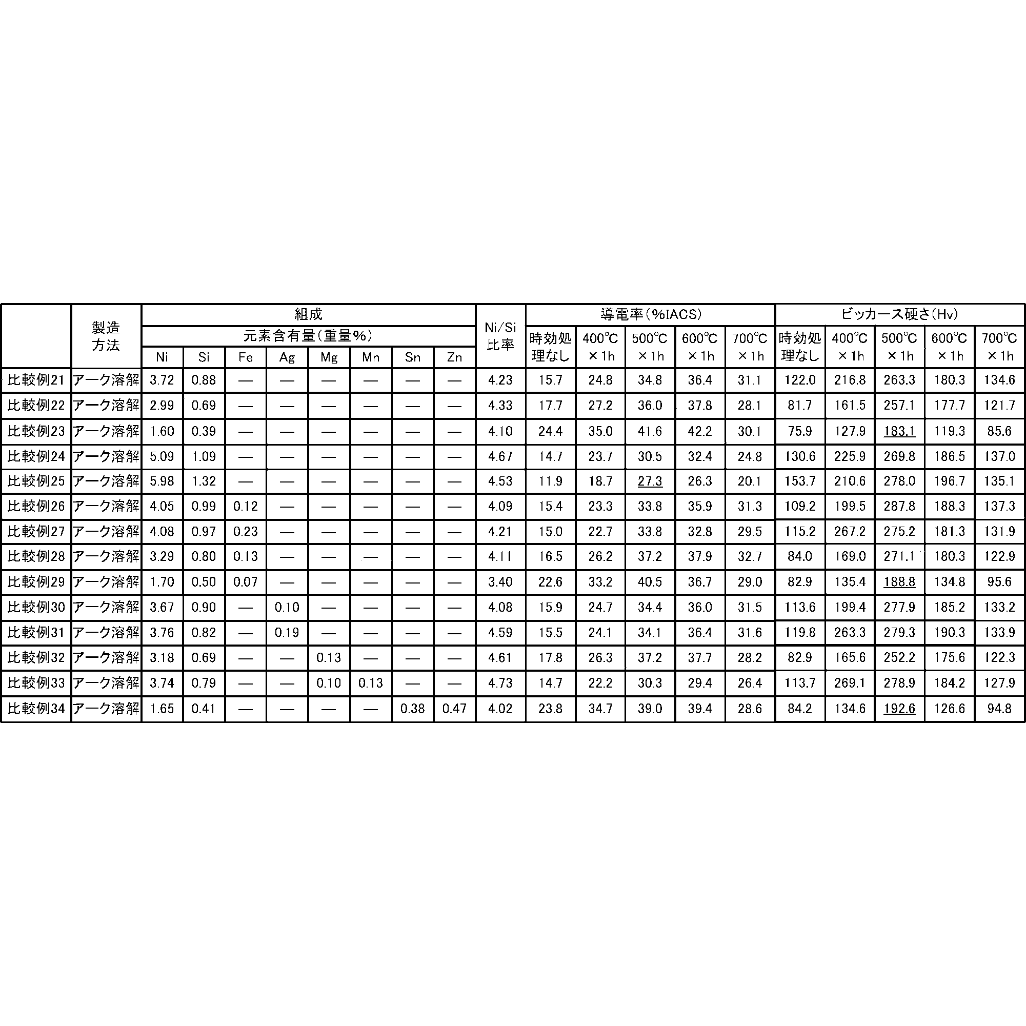
- Table 5 shows the evaluation results of various properties of the arc-melted materials of Comparative Examples 21 to 34.
- the underlined property values indicate values that do not satisfy the condition range for a copper alloy shaped body even after aging treatment at 500°C.
- the rolled arc-melted material was aged in an inert atmosphere at temperatures of 400, 500, 600, and 700°C for 1 hour.
- the electrical conductivity of the arc melted sawn material that had been subjected to aging treatment and rolling processing was measured using an eddy current conductivity meter.
- Vickers hardness was measured using a microhardness tester.
- Table 6 shows the evaluation results of various properties of the arc-melted materials subjected to rolling processing in Comparative Examples 41 to 54.
- the underlined property values indicate values that do not satisfy the condition range for a copper alloy shaped body even after aging treatment at 500°C.
- Figure 5 shows the characteristics of the copper alloy laminate manufactured bodies of Examples 1 to 6 and 10 to 19 after aging treatment at 500°C, the arc melted materials of Comparative Examples 21 to 34, and the rolling processing of Comparative Examples 41 to 54. It is a diagram plotting the characteristics of arc-molten material with electrical conductivity (%IACS) on the X-axis and Vickers hardness (Hv) on the Y-axis.
- %IACS electrical conductivity
- Hv Vickers hardness
Landscapes
- Chemical & Material Sciences (AREA)
- Engineering & Computer Science (AREA)
- Materials Engineering (AREA)
- Manufacturing & Machinery (AREA)
- Mechanical Engineering (AREA)
- Organic Chemistry (AREA)
- Metallurgy (AREA)
- Physics & Mathematics (AREA)
- Plasma & Fusion (AREA)
- Thermal Sciences (AREA)
- Automation & Control Theory (AREA)
- Crystallography & Structural Chemistry (AREA)
- Powder Metallurgy (AREA)
Abstract
Description
積層造形法により積層造形体を造形するために用いられる積層造形用銅合金粉末であって、
ニッケルおよびシリコンを含有し、残部が銅および不可避的不純物からなり、
前記ニッケルの含有量(重量%)を前記シリコンの含有量(重量%)で除した値が3.3以上7.2以下である。
上記の積層造形用銅合金粉末を用いて、積層造形装置により積層造形された銅合金積層造形体であって、
ニッケルの含有量(重量%)をシリコンの含有量(重量%)で除した値が3.3以上7.2以下である。
上記の積層造形用銅合金粉末を用いて、積層造形装置により銅合金積層造形体を積層造形する積層造形工程と、
前記銅合金積層造形体を、450℃以上550℃以下で保持する時効処理工程と、
を含む。
本実施形態においては、ニッケルおよびシリコンを含有し、残部が銅および不可避的不純物からなる積層造形用銅合金粉末と、その積層造形用銅合金粉末を用いて積層造形された銅合金積層造形体について説明する。
本実施形態の積層造形用銅合金粉末の製造方法は特に限定されないが、ガスアトマイズ法、水アトマイズ法、遠心アトマイズ法、プラズマアトマイズ法、プラズマ回転電極法等のように、粉末粒子が溶融状態から急冷凝固される方式が好ましい。量産性の点からは、ガスアトマイズ法が特に好ましい。製造した粉末は、公知の分級方法によって、所定の分級条件にて分級し、適切な粒度の積層造形用銅合金粉末に調整することができる。分級を実施するための分級装置としては、気流分級機を好適に用いることができる。
析出強化型銅合金であるコルソン合金では、基質である銅に過飽和固溶したニッケルおよびシリコンが時効処理によってニッケル-シリコン金属間化合物を生成して析出し、銅合金の強度が向上する。
積層造形用として用いられる粉末には、ホッパーから造形ステージ上への供給工程や、一定の厚みで均一に敷き詰められた粉末層を形成する工程、溶融凝固の工程など、積層造形の各プロセスに適合していることが要求される。そのため、以下の条件が必要とされる。その条件とは、適切な範囲内に調整された粒径、適切な範囲内の見掛密度、供給ホッパーからの供給が可能であり、かつ、適切な粉末層を形成可能とする粉末の流動性である。
銅合金積層造形体の製造方法としては、種々公知の金属積層造形技術を用いることができる。例えば粉末床溶融法では、金属粉末を造形ステージにブレードあるいはローラーなどでならして敷き詰めて粉末層を形成し、形成した粉末層の所定位置にレーザあるいは電子ビームを照射して金属粉末を焼結・溶融させる工程を繰り返しながら積層造形体の作製を行う。金属積層造形の造形プロセスにおいては、高品質な造形体を得るために非常に多数のプロセスパラメータを制御する必要がある。
銅合金積層造形体に時効処理を施すことで、過飽和に固溶したニッケルおよびシリコンが析出し、積層造形体の強度が向上し導電率が向上する。そのため時効処理工程は、本実施形態の高強度かつ高導電率の特性を得るためには必須の工程である。時効処理は、積層造形体を所定の温度に加熱し、所定の時間保持することで実施できる。時効処理は還元性雰囲気もしくは不活性ガス中、真空で行うことが好ましい。
本実施形態においては、ニッケルおよびシリコンと、他の金属元素、例えば鉄、銀、マグネシウム、マンガン、錫、および亜鉛から選択される1種または2種以上を含有し、残部が銅および不可避的不純物からなる積層造形用銅合金粉末と、その積層造形用銅合金粉末を用いて積層造形した銅合金積層造形体について説明する。
本実施形態においては、積層造形により造形された銅合金積層造形体と、従来のアーク溶解または圧延加工によって製造された銅合金積層造形体との特性の比較結果について説明する。
以上、実施形態を参照して本発明を説明したが、本発明は上記実施形態に限定されるものではない。本発明の構成や詳細には、本発明の技術的範囲で当業者が理解し得る様々な変更をすることができる。また、それぞれの実施形態に含まれる別々の特徴を如何様に組み合わせた技術も、本発明の技術的範囲に含まれる。
ニッケルとシリコンとの含有量および含有比率を変化させてニッケルとシリコンとを含有する積層造形用銅合金粉末を製造し、次に積層造形用銅合金粉末を用いて積層造形された銅合金積層造形体を製造し、それらの特性を測定した。
ガスアトマイズ法により、表1に示したニッケルとシリコンとを含有する銅合金の積層造形用銅合金粉末を製造した。そして、得られた積層造形用銅合金粉末を、レーザ方式粉末床溶融法向けとして粒径10μm以上45μm以下に、電子ビーム方式粉末床溶融法向けとして粒径45μm以上105μm以下となるように分級した。

実施例1~6および比較例5~12においては、スキージング性が十分であり、良好に銅合金積層造形体が製造できた。
実施例1~5および比較例5~12の積層造形用銅合金粉末を用いて、波長1064nmのYbファイバレーザ搭載の3D粉末積層造形機(SLM Solutions GmbH、SLM280HL)にて試験に供する積層造形体を製造した。積層造形は、積層厚25μm以上50μm以下、レーザ出力300W以上700W以下、走査速度900mm/sec以上1500mm/sec以下、エネルギー密度150J/mm3以上450J/mm3以下の条件で行った。
実施例1~6および比較例5~12の銅合金積層造形用粉末を用いて製造した積層造形体の相対密度(%)を、置換媒体としてヘリウムガスを使用したアルキメデス法により測定した(AccuPyc1330:株式会社島津製作所製)。測定結果は表2に示した。
ニッケルとシリコンとの含有量および含有比率と、他の金属元素の含有量とを変化させて積層造形用銅合金粉末を製造し、次に積層造形用銅合金粉末を用いて積層造形された銅合金積層造形体を製造し、それらの特性を測定した。
ガスアトマイズ法により、表3に示したニッケルおよびシリコンと、他の金属元素とを含有する銅合金の積層造形用銅合金粉末を製造した。そして、得られた積層造形用銅合金粉末を、レーザ方式粉末床溶融法向けとして粒径10μm以上45μm以下に、電子ビーム方式粉末床溶融法向けとして粒径45μm以上105μm以下となるように分級した。

実施例10~13および15~19の積層造形用銅合金粉末を用いて、波長1064nmのYbファイバレーザ搭載の3D粉末積層造形機(SLM Solutions GmbH、SLM280HL)にて試験に供する積層造形体を製造した。積層造形は、積層厚25μm以上50μm以下、レーザ出力300W以上700W以下、走査速度900mm/sec以上1500mm/sec以下、エネルギー密度150J/mm3以上450J/mm3以下の条件で行った。
実施例10~19の銅合金積層造形用粉末を用いて製造した積層造形体の相対密度(%)を、置換媒体としてヘリウムガスを使用したアルキメデス法により測定した(AccuPyc1330:株式会社島津製作所製)。測定結果は表4に示した。

(アーク溶製材)
鋳造したコルソン合金インゴットに塑性加工および溶体化処理を施す従来の製造方法を用いて作製した銅合金(コルソン合金)の特性と、実施例1~6および10~19の銅合金積層造形体の特性を比較するため、以下の方法を用いて従来法で作製されたコルソン合金の特性評価を行った。鋳造材製造方法の代わりとして、公知の溶製材製造方法であるアーク溶解法を用いた。
次に、得られた比較例21~34のアーク溶製材を、圧延装置を用いて加工率50%で圧延し、塑性加工を行った。その圧延体に、不活性雰囲気中で950℃に温度を設定して1時間の溶体化処理を施した。この圧延加工を加えたアーク溶製材を比較例41~54とした。

Claims (13)
- 積層造形法により積層造形体を造形するために用いられる積層造形用銅合金粉末であって、
ニッケルおよびシリコンを含有し、残部が銅および不可避的不純物からなり、
前記ニッケルの含有量(重量%)を前記シリコンの含有量(重量%)で除した値が3.3以上7.2以下である積層造形用銅合金粉末。 - 前記ニッケルを1.5重量%以上6.0重量%以下含有する請求項1に記載の積層造形用銅合金粉末。
- 前記シリコンを0.35重量%以上1.5重量%以下含有する請求項2に記載の積層造形用銅合金粉末。
- 50%粒径が3μm以上200μm以下である請求項1から3のいずれか1項に記載の積層造形用銅合金粉末。
- JIS Z 2504(ISO 3923-1)の測定法で測定したときの粉末の見掛密度が3.5g/cm3以上である請求項1から3のいずれか1項に記載の積層造形用銅合金粉末。
- せん断試験によって得られた破壊包絡線から求めた銅合金粉末の付着力が、0.600kPa以下である請求項1から3のいずれか1項に記載の積層造形用銅合金粉末。
- さらに、鉄、銀、マグネシウム、マンガン、錫および亜鉛から選択される1種または2種以上を合計で1.0重量%(ただし、鉄、銀、マグネシウム、マンガン、錫、および亜鉛が0重量%である場合を除く)まで含有する請求項1から3のいずれか1項に記載の積層造形用銅合金粉末。
- 請求項1に記載の積層造形用銅合金粉末を用いて、積層造形装置により積層造形された銅合金積層造形体であって、
ニッケルの含有量(重量%)をシリコンの含有量(重量%)で除した値が3.3以上7.2以下である銅合金積層造形体。 - 請求項3に記載の積層造形用銅合金粉末を用いて、積層造形装置により積層造形された銅合金積層造形体であって、
ニッケルの含有量(重量%)をシリコンの含有量(重量%)で除した値が3.3以上7.2以下であり、
前記ニッケルを1.5重量%以上6.0重量%以下、および、前記シリコンを0.35重量%以上1.5重量%以下含有し、残部が銅および不可避的不純物からなる銅合金積層造形体。 - 請求項8または9に記載の銅合金積層造形体であって、
30%IACS以上の導電率、および、200Hv以上のビッカース硬さを有する銅合金積層造形体。 - 請求項7に記載の積層造形用銅合金粉末を用いて、積層造形装置により積層造形された銅合金積層造形体であって、
ニッケルの含有量(重量%)をシリコンの含有量(重量%)で除した値が3.3以上7.2以下であり、
前記ニッケルを1.5重量%以上6.0重量%以下、前記シリコンを0.35重量%以上1.5重量%以下、および、鉄、銀、マグネシウム、マンガン、錫、および亜鉛から選択される1種または2種以上を合計で1.0重量%(ただし、鉄、銀、マグネシウム、マンガン、錫、および亜鉛が0重量%である場合を除く)まで含有し、残部が銅および不可避的不純物からなる銅合金積層造形体。 - 請求項11に記載の銅合金積層造形体であって、
30%IACS以上の導電率、および、200Hv以上のビッカース硬さを有する銅合金積層造形体。 - 請求項1から3のいずれか1項に記載の積層造形用銅合金粉末を用いて、積層造形装置により銅合金積層造形体を積層造形する積層造形工程と、
前記銅合金積層造形体を、450℃以上550℃以下で保持する時効処理工程と、
を含む銅合金積層造形体の製造方法。
Priority Applications (5)
| Application Number | Priority Date | Filing Date | Title |
|---|---|---|---|
| EP22948014.0A EP4541484A4 (en) | 2022-06-24 | 2022-06-24 | COPPER ALLOY POWDER FOR ADDITIVE MANUFACTURING, ADDITIVELY MANUFACTURED COPPER ALLOY ARTICLE, AND METHOD FOR MANUFACTURING ADDITIVELY MANUFACTURED COPPER ALLOY ARTICLE |
| JP2024528230A JP7789207B2 (ja) | 2022-06-24 | 2022-06-24 | 積層造形用銅合金粉末、銅合金積層造形体および銅合金積層造形体の製造方法 |
| KR1020257002771A KR20250029188A (ko) | 2022-06-24 | 2022-06-24 | 적층조형용 구리합금 분말, 구리합금 적층조형체 및 구리합금 적층조형체의 제조 방법 |
| CN202280097400.1A CN119421752A (zh) | 2022-06-24 | 2022-06-24 | 层叠造形用铜合金粉末、铜合金层叠造形体及铜合金层叠造形体的制造方法 |
| PCT/JP2022/025245 WO2023248453A1 (ja) | 2022-06-24 | 2022-06-24 | 積層造形用銅合金粉末、銅合金積層造形体および銅合金積層造形体の製造方法 |
Applications Claiming Priority (1)
| Application Number | Priority Date | Filing Date | Title |
|---|---|---|---|
| PCT/JP2022/025245 WO2023248453A1 (ja) | 2022-06-24 | 2022-06-24 | 積層造形用銅合金粉末、銅合金積層造形体および銅合金積層造形体の製造方法 |
Publications (1)
| Publication Number | Publication Date |
|---|---|
| WO2023248453A1 true WO2023248453A1 (ja) | 2023-12-28 |
Family
ID=89379328
Family Applications (1)
| Application Number | Title | Priority Date | Filing Date |
|---|---|---|---|
| PCT/JP2022/025245 Ceased WO2023248453A1 (ja) | 2022-06-24 | 2022-06-24 | 積層造形用銅合金粉末、銅合金積層造形体および銅合金積層造形体の製造方法 |
Country Status (5)
| Country | Link |
|---|---|
| EP (1) | EP4541484A4 (ja) |
| JP (1) | JP7789207B2 (ja) |
| KR (1) | KR20250029188A (ja) |
| CN (1) | CN119421752A (ja) |
| WO (1) | WO2023248453A1 (ja) |
Citations (7)
| Publication number | Priority date | Publication date | Assignee | Title |
|---|---|---|---|---|
| JPH0931571A (ja) * | 1995-07-17 | 1997-02-04 | Hitachi Powdered Metals Co Ltd | 耐摩耗性銅系焼結合金 |
| JP2005256147A (ja) * | 2004-03-15 | 2005-09-22 | Toyota Motor Corp | 肉盛耐摩耗銅基合金 |
| JP2011157630A (ja) * | 2002-07-05 | 2011-08-18 | Olin Corp | コバルト、ニッケル、珪素を含む銅合金 |
| WO2018062527A1 (ja) * | 2016-09-29 | 2018-04-05 | Jx金属株式会社 | レーザー焼結用表面処理金属粉 |
| JP2018123405A (ja) * | 2017-02-03 | 2018-08-09 | 日産自動車株式会社 | 積層部材の製造方法 |
| US20180311736A1 (en) * | 2017-04-28 | 2018-11-01 | Te Connectivity Corporation | System and Method for Forming Nano-Particles in Additively-Manufactured Metal Alloys |
| JP2021017639A (ja) | 2019-07-23 | 2021-02-15 | 山陽特殊製鋼株式会社 | Cu基合金粉末 |
Family Cites Families (5)
| Publication number | Priority date | Publication date | Assignee | Title |
|---|---|---|---|---|
| MY193663A (en) * | 2015-08-06 | 2022-10-24 | Nissan Motor | Sliding member and manufacturing method therefor |
| WO2018079304A1 (ja) * | 2016-10-25 | 2018-05-03 | 株式会社ダイヘン | 銅合金粉末、積層造形物の製造方法および積層造形物 |
| JP6854140B2 (ja) | 2017-02-03 | 2021-04-07 | 日産自動車株式会社 | 積層体、摺動部材、及び積層体の製造方法 |
| JP7119380B2 (ja) | 2018-01-18 | 2022-08-17 | 三菱マテリアル株式会社 | 銅粉末及びその製造方法 |
| JP7575209B2 (ja) | 2020-07-07 | 2024-10-29 | 古河電気工業株式会社 | 銅合金材およびその製造方法 |
-
2022
- 2022-06-24 EP EP22948014.0A patent/EP4541484A4/en active Pending
- 2022-06-24 JP JP2024528230A patent/JP7789207B2/ja active Active
- 2022-06-24 WO PCT/JP2022/025245 patent/WO2023248453A1/ja not_active Ceased
- 2022-06-24 CN CN202280097400.1A patent/CN119421752A/zh active Pending
- 2022-06-24 KR KR1020257002771A patent/KR20250029188A/ko active Pending
Patent Citations (7)
| Publication number | Priority date | Publication date | Assignee | Title |
|---|---|---|---|---|
| JPH0931571A (ja) * | 1995-07-17 | 1997-02-04 | Hitachi Powdered Metals Co Ltd | 耐摩耗性銅系焼結合金 |
| JP2011157630A (ja) * | 2002-07-05 | 2011-08-18 | Olin Corp | コバルト、ニッケル、珪素を含む銅合金 |
| JP2005256147A (ja) * | 2004-03-15 | 2005-09-22 | Toyota Motor Corp | 肉盛耐摩耗銅基合金 |
| WO2018062527A1 (ja) * | 2016-09-29 | 2018-04-05 | Jx金属株式会社 | レーザー焼結用表面処理金属粉 |
| JP2018123405A (ja) * | 2017-02-03 | 2018-08-09 | 日産自動車株式会社 | 積層部材の製造方法 |
| US20180311736A1 (en) * | 2017-04-28 | 2018-11-01 | Te Connectivity Corporation | System and Method for Forming Nano-Particles in Additively-Manufactured Metal Alloys |
| JP2021017639A (ja) | 2019-07-23 | 2021-02-15 | 山陽特殊製鋼株式会社 | Cu基合金粉末 |
Non-Patent Citations (1)
| Title |
|---|
| See also references of EP4541484A4 |
Also Published As
| Publication number | Publication date |
|---|---|
| JP7789207B2 (ja) | 2025-12-19 |
| CN119421752A (zh) | 2025-02-11 |
| EP4541484A1 (en) | 2025-04-23 |
| EP4541484A4 (en) | 2025-09-03 |
| JPWO2023248453A1 (ja) | 2023-12-28 |
| KR20250029188A (ko) | 2025-03-04 |
Similar Documents
| Publication | Publication Date | Title |
|---|---|---|
| JP7630554B2 (ja) | 銅合金粉末、積層造形物および積層造形物の製造方法ならびに各種金属部品 | |
| JP7314184B2 (ja) | アルミニウム合金からなる部品の製造方法 | |
| CN108431262B (zh) | 高熵合金构件、该合金构件的制造方法、及使用了该合金构件的制造物 | |
| EP3616810A1 (en) | High-strength aluminum alloy laminated molding and production method therefor | |
| CN113348262A (zh) | 制造铝合金零件的方法 | |
| EP4005700B1 (en) | Cu-based alloy powder | |
| JP2017155291A (ja) | 高強度アルミニウム合金積層成形体の製造方法 | |
| JP2016053198A (ja) | 金属成形体および金属成形体用金属粉末 | |
| EP3804879A1 (en) | Cu-based alloy powder | |
| JP7626286B2 (ja) | 金属am用銅合金粉末の製造方法 | |
| JP7394241B2 (ja) | 積層造形用銅合金粉末とその評価方法、銅合金積層造形体の製造方法および銅合金積層造形体 | |
| KR20230009373A (ko) | 알루미늄 합금 부품을 제조하기 위한 방법 | |
| EP3760342B1 (en) | Copper alloy powder having excellent laser absorptivity | |
| WO2023248453A1 (ja) | 積層造形用銅合金粉末、銅合金積層造形体および銅合金積層造形体の製造方法 | |
| JP7774710B2 (ja) | 積層造形用銅合金粉末とその製造方法および評価方法、銅合金積層造形体の製造方法および銅合金積層造形体 | |
| HK40115481A (zh) | 层叠造形用铜合金粉末、铜合金层叠造形体及铜合金层叠造形体的制造方法 | |
| HK40092778A (zh) | 层叠造形用铜合金粉末及其评价方法、铜合金层叠造形体的制造方法及铜合金层叠造形体 | |
| HK40112428A (zh) | 层叠造形用铜合金粉末和其制造方法及评价方法、铜合金层叠造形体的制造方法及铜合金层叠造形体 | |
| TWI908435B (zh) | 積層造形用金屬粉末及積層造形體 | |
| JP2026003389A (ja) | アルミニウム合金積層造形体及びその製造方法 | |
| Kim et al. | Microstructures and mechanical properties of CNT/AZ31 composites produced by mechanical alloying | |
| WO2024090449A1 (ja) | 金属am銅合金粉末および積層造形物の製造方法 |
Legal Events
| Date | Code | Title | Description |
|---|---|---|---|
| 121 | Ep: the epo has been informed by wipo that ep was designated in this application |
Ref document number: 22948014 Country of ref document: EP Kind code of ref document: A1 |
|
| ENP | Entry into the national phase |
Ref document number: 2024528230 Country of ref document: JP Kind code of ref document: A |
|
| WWE | Wipo information: entry into national phase |
Ref document number: 202280097400.1 Country of ref document: CN |
|
| WWE | Wipo information: entry into national phase |
Ref document number: 2022948014 Country of ref document: EP |
|
| WWE | Wipo information: entry into national phase |
Ref document number: 202547004008 Country of ref document: IN |
|
| ENP | Entry into the national phase |
Ref document number: 20257002771 Country of ref document: KR Kind code of ref document: A |
|
| NENP | Non-entry into the national phase |
Ref country code: DE |
|
| ENP | Entry into the national phase |
Ref document number: 2022948014 Country of ref document: EP Effective date: 20250115 |
|
| WWP | Wipo information: published in national office |
Ref document number: 202280097400.1 Country of ref document: CN |
|
| WWP | Wipo information: published in national office |
Ref document number: 1020257002771 Country of ref document: KR |
|
| WWP | Wipo information: published in national office |
Ref document number: 2022948014 Country of ref document: EP |