WO2023281850A1 - 照明光学系および露光装置 - Google Patents
照明光学系および露光装置 Download PDFInfo
- Publication number
- WO2023281850A1 WO2023281850A1 PCT/JP2022/013874 JP2022013874W WO2023281850A1 WO 2023281850 A1 WO2023281850 A1 WO 2023281850A1 JP 2022013874 W JP2022013874 W JP 2022013874W WO 2023281850 A1 WO2023281850 A1 WO 2023281850A1
- Authority
- WO
- WIPO (PCT)
- Prior art keywords
- light
- lens
- optical system
- illumination optical
- elements
- Prior art date
- Legal status (The legal status is an assumption and is not a legal conclusion. Google has not performed a legal analysis and makes no representation as to the accuracy of the status listed.)
- Ceased
Links
Images



Classifications
-
- F—MECHANICAL ENGINEERING; LIGHTING; HEATING; WEAPONS; BLASTING
- F21—LIGHTING
- F21V—FUNCTIONAL FEATURES OR DETAILS OF LIGHTING DEVICES OR SYSTEMS THEREOF; STRUCTURAL COMBINATIONS OF LIGHTING DEVICES WITH OTHER ARTICLES, NOT OTHERWISE PROVIDED FOR
- F21V5/00—Refractors for light sources
- F21V5/02—Refractors for light sources of prismatic shape
-
- G—PHYSICS
- G02—OPTICS
- G02B—OPTICAL ELEMENTS, SYSTEMS OR APPARATUS
- G02B19/00—Condensers, e.g. light collectors or similar non-imaging optics
- G02B19/0004—Condensers, e.g. light collectors or similar non-imaging optics characterised by the optical means employed
- G02B19/0009—Condensers, e.g. light collectors or similar non-imaging optics characterised by the optical means employed having refractive surfaces only
- G02B19/0014—Condensers, e.g. light collectors or similar non-imaging optics characterised by the optical means employed having refractive surfaces only at least one surface having optical power
-
- G—PHYSICS
- G03—PHOTOGRAPHY; CINEMATOGRAPHY; ANALOGOUS TECHNIQUES USING WAVES OTHER THAN OPTICAL WAVES; ELECTROGRAPHY; HOLOGRAPHY
- G03F—PHOTOMECHANICAL PRODUCTION OF TEXTURED OR PATTERNED SURFACES, e.g. FOR PRINTING, FOR PROCESSING OF SEMICONDUCTOR DEVICES; MATERIALS THEREFOR; ORIGINALS THEREFOR; APPARATUS SPECIALLY ADAPTED THEREFOR
- G03F7/00—Photomechanical, e.g. photolithographic, production of textured or patterned surfaces, e.g. printing surfaces; Materials therefor, e.g. comprising photoresists; Apparatus specially adapted therefor
- G03F7/70—Microphotolithographic exposure; Apparatus therefor
- G03F7/70216—Mask projection systems
- G03F7/70308—Optical correction elements, filters or phase plates for manipulating imaging light, e.g. intensity, wavelength, polarisation, phase or image shift
-
- F—MECHANICAL ENGINEERING; LIGHTING; HEATING; WEAPONS; BLASTING
- F21—LIGHTING
- F21K—NON-ELECTRIC LIGHT SOURCES USING LUMINESCENCE; LIGHT SOURCES USING ELECTROCHEMILUMINESCENCE; LIGHT SOURCES USING CHARGES OF COMBUSTIBLE MATERIAL; LIGHT SOURCES USING SEMICONDUCTOR DEVICES AS LIGHT-GENERATING ELEMENTS; LIGHT SOURCES NOT OTHERWISE PROVIDED FOR
- F21K9/00—Light sources using semiconductor devices as light-generating elements, e.g. using light-emitting diodes [LED] or lasers
- F21K9/60—Optical arrangements integrated in the light source, e.g. for improving the colour rendering index or the light extraction
- F21K9/69—Details of refractors forming part of the light source
-
- F—MECHANICAL ENGINEERING; LIGHTING; HEATING; WEAPONS; BLASTING
- F21—LIGHTING
- F21V—FUNCTIONAL FEATURES OR DETAILS OF LIGHTING DEVICES OR SYSTEMS THEREOF; STRUCTURAL COMBINATIONS OF LIGHTING DEVICES WITH OTHER ARTICLES, NOT OTHERWISE PROVIDED FOR
- F21V5/00—Refractors for light sources
- F21V5/007—Array of lenses or refractors for a cluster of light sources, e.g. for arrangement of multiple light sources in one plane
-
- G—PHYSICS
- G02—OPTICS
- G02B—OPTICAL ELEMENTS, SYSTEMS OR APPARATUS
- G02B19/00—Condensers, e.g. light collectors or similar non-imaging optics
-
- G—PHYSICS
- G02—OPTICS
- G02B—OPTICAL ELEMENTS, SYSTEMS OR APPARATUS
- G02B19/00—Condensers, e.g. light collectors or similar non-imaging optics
- G02B19/0033—Condensers, e.g. light collectors or similar non-imaging optics characterised by the use
- G02B19/0047—Condensers, e.g. light collectors or similar non-imaging optics characterised by the use for use with a light source
- G02B19/0052—Condensers, e.g. light collectors or similar non-imaging optics characterised by the use for use with a light source the light source comprising a laser diode
-
- G—PHYSICS
- G02—OPTICS
- G02B—OPTICAL ELEMENTS, SYSTEMS OR APPARATUS
- G02B19/00—Condensers, e.g. light collectors or similar non-imaging optics
- G02B19/0033—Condensers, e.g. light collectors or similar non-imaging optics characterised by the use
- G02B19/0047—Condensers, e.g. light collectors or similar non-imaging optics characterised by the use for use with a light source
- G02B19/0052—Condensers, e.g. light collectors or similar non-imaging optics characterised by the use for use with a light source the light source comprising a laser diode
- G02B19/0057—Condensers, e.g. light collectors or similar non-imaging optics characterised by the use for use with a light source the light source comprising a laser diode in the form of a laser diode array, e.g. laser diode bar
-
- G—PHYSICS
- G02—OPTICS
- G02B—OPTICAL ELEMENTS, SYSTEMS OR APPARATUS
- G02B19/00—Condensers, e.g. light collectors or similar non-imaging optics
- G02B19/0033—Condensers, e.g. light collectors or similar non-imaging optics characterised by the use
- G02B19/0047—Condensers, e.g. light collectors or similar non-imaging optics characterised by the use for use with a light source
- G02B19/0061—Condensers, e.g. light collectors or similar non-imaging optics characterised by the use for use with a light source the light source comprising a LED
-
- G—PHYSICS
- G02—OPTICS
- G02B—OPTICAL ELEMENTS, SYSTEMS OR APPARATUS
- G02B19/00—Condensers, e.g. light collectors or similar non-imaging optics
- G02B19/0033—Condensers, e.g. light collectors or similar non-imaging optics characterised by the use
- G02B19/0047—Condensers, e.g. light collectors or similar non-imaging optics characterised by the use for use with a light source
- G02B19/0061—Condensers, e.g. light collectors or similar non-imaging optics characterised by the use for use with a light source the light source comprising a LED
- G02B19/0066—Condensers, e.g. light collectors or similar non-imaging optics characterised by the use for use with a light source the light source comprising a LED in the form of an LED array
-
- G—PHYSICS
- G02—OPTICS
- G02B—OPTICAL ELEMENTS, SYSTEMS OR APPARATUS
- G02B27/00—Optical systems or apparatus not provided for by any of the groups G02B1/00 - G02B26/00, G02B30/00
- G02B27/09—Beam shaping, e.g. changing the cross-sectional area, not otherwise provided for
- G02B27/0905—Dividing and/or superposing multiple light beams
-
- G—PHYSICS
- G02—OPTICS
- G02B—OPTICAL ELEMENTS, SYSTEMS OR APPARATUS
- G02B27/00—Optical systems or apparatus not provided for by any of the groups G02B1/00 - G02B26/00, G02B30/00
- G02B27/09—Beam shaping, e.g. changing the cross-sectional area, not otherwise provided for
- G02B27/0927—Systems for changing the beam intensity distribution, e.g. Gaussian to top-hat
-
- G—PHYSICS
- G02—OPTICS
- G02B—OPTICAL ELEMENTS, SYSTEMS OR APPARATUS
- G02B27/00—Optical systems or apparatus not provided for by any of the groups G02B1/00 - G02B26/00, G02B30/00
- G02B27/09—Beam shaping, e.g. changing the cross-sectional area, not otherwise provided for
- G02B27/0938—Using specific optical elements
- G02B27/095—Refractive optical elements
- G02B27/0955—Lenses
-
- G—PHYSICS
- G02—OPTICS
- G02B—OPTICAL ELEMENTS, SYSTEMS OR APPARATUS
- G02B27/00—Optical systems or apparatus not provided for by any of the groups G02B1/00 - G02B26/00, G02B30/00
- G02B27/09—Beam shaping, e.g. changing the cross-sectional area, not otherwise provided for
- G02B27/0938—Using specific optical elements
- G02B27/095—Refractive optical elements
- G02B27/0955—Lenses
- G02B27/0961—Lens arrays
-
- G—PHYSICS
- G02—OPTICS
- G02B—OPTICAL ELEMENTS, SYSTEMS OR APPARATUS
- G02B3/00—Simple or compound lenses
- G02B3/0006—Arrays
-
- G—PHYSICS
- G02—OPTICS
- G02B—OPTICAL ELEMENTS, SYSTEMS OR APPARATUS
- G02B3/00—Simple or compound lenses
- G02B3/0006—Arrays
- G02B3/0037—Arrays characterized by the distribution or form of lenses
- G02B3/0056—Arrays characterized by the distribution or form of lenses arranged along two different directions in a plane, e.g. honeycomb arrangement of lenses
-
- G—PHYSICS
- G02—OPTICS
- G02B—OPTICAL ELEMENTS, SYSTEMS OR APPARATUS
- G02B3/00—Simple or compound lenses
- G02B3/0006—Arrays
- G02B3/0037—Arrays characterized by the distribution or form of lenses
- G02B3/0062—Stacked lens arrays, i.e. refractive surfaces arranged in at least two planes, without structurally separate optical elements in-between
-
- G—PHYSICS
- G03—PHOTOGRAPHY; CINEMATOGRAPHY; ANALOGOUS TECHNIQUES USING WAVES OTHER THAN OPTICAL WAVES; ELECTROGRAPHY; HOLOGRAPHY
- G03F—PHOTOMECHANICAL PRODUCTION OF TEXTURED OR PATTERNED SURFACES, e.g. FOR PRINTING, FOR PROCESSING OF SEMICONDUCTOR DEVICES; MATERIALS THEREFOR; ORIGINALS THEREFOR; APPARATUS SPECIALLY ADAPTED THEREFOR
- G03F7/00—Photomechanical, e.g. photolithographic, production of textured or patterned surfaces, e.g. printing surfaces; Materials therefor, e.g. comprising photoresists; Apparatus specially adapted therefor
- G03F7/20—Exposure; Apparatus therefor
-
- G—PHYSICS
- G03—PHOTOGRAPHY; CINEMATOGRAPHY; ANALOGOUS TECHNIQUES USING WAVES OTHER THAN OPTICAL WAVES; ELECTROGRAPHY; HOLOGRAPHY
- G03F—PHOTOMECHANICAL PRODUCTION OF TEXTURED OR PATTERNED SURFACES, e.g. FOR PRINTING, FOR PROCESSING OF SEMICONDUCTOR DEVICES; MATERIALS THEREFOR; ORIGINALS THEREFOR; APPARATUS SPECIALLY ADAPTED THEREFOR
- G03F7/00—Photomechanical, e.g. photolithographic, production of textured or patterned surfaces, e.g. printing surfaces; Materials therefor, e.g. comprising photoresists; Apparatus specially adapted therefor
- G03F7/70—Microphotolithographic exposure; Apparatus therefor
- G03F7/70008—Production of exposure light, i.e. light sources
- G03F7/7005—Production of exposure light, i.e. light sources by multiple sources, e.g. light-emitting diodes [LED] or light source arrays
-
- G—PHYSICS
- G03—PHOTOGRAPHY; CINEMATOGRAPHY; ANALOGOUS TECHNIQUES USING WAVES OTHER THAN OPTICAL WAVES; ELECTROGRAPHY; HOLOGRAPHY
- G03F—PHOTOMECHANICAL PRODUCTION OF TEXTURED OR PATTERNED SURFACES, e.g. FOR PRINTING, FOR PROCESSING OF SEMICONDUCTOR DEVICES; MATERIALS THEREFOR; ORIGINALS THEREFOR; APPARATUS SPECIALLY ADAPTED THEREFOR
- G03F7/00—Photomechanical, e.g. photolithographic, production of textured or patterned surfaces, e.g. printing surfaces; Materials therefor, e.g. comprising photoresists; Apparatus specially adapted therefor
- G03F7/70—Microphotolithographic exposure; Apparatus therefor
- G03F7/70058—Mask illumination systems
- G03F7/70075—Homogenization of illumination intensity in the mask plane by using an integrator, e.g. fly's eye lens, facet mirror or glass rod, by using a diffusing optical element or by beam deflection
-
- G—PHYSICS
- G03—PHOTOGRAPHY; CINEMATOGRAPHY; ANALOGOUS TECHNIQUES USING WAVES OTHER THAN OPTICAL WAVES; ELECTROGRAPHY; HOLOGRAPHY
- G03F—PHOTOMECHANICAL PRODUCTION OF TEXTURED OR PATTERNED SURFACES, e.g. FOR PRINTING, FOR PROCESSING OF SEMICONDUCTOR DEVICES; MATERIALS THEREFOR; ORIGINALS THEREFOR; APPARATUS SPECIALLY ADAPTED THEREFOR
- G03F7/00—Photomechanical, e.g. photolithographic, production of textured or patterned surfaces, e.g. printing surfaces; Materials therefor, e.g. comprising photoresists; Apparatus specially adapted therefor
- G03F7/70—Microphotolithographic exposure; Apparatus therefor
- G03F7/70216—Mask projection systems
- G03F7/70316—Details of optical elements, e.g. of Bragg reflectors, extreme ultraviolet [EUV] multilayer or bilayer mirrors or diffractive optical elements
-
- G—PHYSICS
- G03—PHOTOGRAPHY; CINEMATOGRAPHY; ANALOGOUS TECHNIQUES USING WAVES OTHER THAN OPTICAL WAVES; ELECTROGRAPHY; HOLOGRAPHY
- G03F—PHOTOMECHANICAL PRODUCTION OF TEXTURED OR PATTERNED SURFACES, e.g. FOR PRINTING, FOR PROCESSING OF SEMICONDUCTOR DEVICES; MATERIALS THEREFOR; ORIGINALS THEREFOR; APPARATUS SPECIALLY ADAPTED THEREFOR
- G03F7/00—Photomechanical, e.g. photolithographic, production of textured or patterned surfaces, e.g. printing surfaces; Materials therefor, e.g. comprising photoresists; Apparatus specially adapted therefor
- G03F7/70—Microphotolithographic exposure; Apparatus therefor
- G03F7/70483—Information management; Active and passive control; Testing; Wafer monitoring, e.g. pattern monitoring
- G03F7/7055—Exposure light control in all parts of the microlithographic apparatus, e.g. pulse length control or light interruption
- G03F7/70583—Speckle reduction, e.g. coherence control or amplitude/wavefront splitting
-
- F—MECHANICAL ENGINEERING; LIGHTING; HEATING; WEAPONS; BLASTING
- F21—LIGHTING
- F21Y—INDEXING SCHEME ASSOCIATED WITH SUBCLASSES F21K, F21L, F21S and F21V, RELATING TO THE FORM OR THE KIND OF THE LIGHT SOURCES OR OF THE COLOUR OF THE LIGHT EMITTED
- F21Y2115/00—Light-generating elements of semiconductor light sources
Definitions
- the present invention relates to illumination optical systems and exposure apparatuses.
- Exposure apparatuses and illumination optical systems used in the manufacturing processes of semiconductor devices, flat panel displays, MEMS (Micro Electro Mechanical Systems), etc. are known.
- high-intensity discharge lamps such as ultra-high pressure mercury lamps and metal halide lamps have been used as light sources for exposure equipment.
- light-emitting elements such as LEDs and LDs
- a technology has been proposed in which a plurality of LEDs are used as the light source of an exposure apparatus.
- LEDs emit a small amount of light per chip as a light source for exposure. Therefore, in order to obtain the required high illuminance on the surface to be illuminated, it is required that the light from the plurality of chips be combined by an illumination optical system and guided to the surface to be illuminated.
- Patent Document 1 the images of the light emitting surfaces of a plurality of LEDs are enlarged to a size that covers the effective area of the incident side surface of the fly's eye lens, and the enlarged images overlap each other on the incident side of the fly's eye lens.
- An illumination optical system and an exposure apparatus are disclosed.
- an object of the present invention is to utilize light from a plurality of light emitting elements with high efficiency.
- an illumination optical system is a light source in which a plurality of light emitting elements each emitting light from a light emitting surface are arranged in a direction in which the light emitting surface spreads; a relay optical system that converts a light distribution of light emitted by an element into an illuminance distribution and superimposes a plurality of the illuminance distributions corresponding to the plurality of light emitting elements on a superimposed plane; and light emitted by the relay optical system.
- an optical integrator in which a plurality of wavefront splitting elements for wavefront splitting and transmitting the light as a plurality of light beams are arranged in parallel, and a condenser optical system for superimposing the plurality of light beams on an illuminated surface.
- the light from each light emitting element is superimposed on the overlapping surface as a round illuminance distribution, and the light passing through the round aperture stop is directed to the condenser optical system. It is highly efficient in guiding and highly efficient in utilizing the light emitted from the light source.
- the relay optical system has a plurality of first lens elements corresponding to the plurality of light emitting elements, and a condensing lens group in which each first lens converges the light from each light emitting element. and a plurality of second lens elements corresponding to the plurality of first lens elements, wherein irradiated light having an illuminance distribution corresponding to the light distribution of light from each light emitting element is transmitted through each first lens to each second lens element. and the output surface of each second lens element of the lens array to optically cooperate with each other to superimpose the irradiation light applied to the entrance surface of each second lens element. and a relay lens directed onto the surface and overlapping each other.
- the function of the relay optical system is shared by the condenser lens group, the lens array, and the relay lens, and the relay optical system is easily realized.
- the distance from the relay lens to the entrance surface of the optical integrator is preferably shorter than the distance from the relay lens to the superimposition surface. Even if the incident surface of the optical integrator is positioned at this distance, the light utilization efficiency is almost unchanged and the illuminance distribution is flat to the periphery on the surface of the aperture stop, making it suitable for exposure of finer patterns.
- each of the plurality of second lens elements has a rectangular outer shape when viewed in a direction along the optical axis, and the plurality of second lens elements are bundled. is also preferred.
- the use of square second lens elements improves light utilization efficiency compared to the case where round second lens elements are used.
- the output sides of the plurality of first lens elements each have a rectangular outer shape when viewed along the optical axis, and the plurality of first lens elements Bundled is also preferred.
- the first lens element having a square shape on the output side the light utilization efficiency is improved compared to the case where the round first lens element is used.
- each of the plurality of first lens elements in the condenser lens group is composed of a front element positioned on the light emitting element side and a rear element positioned on the lens array side.
- the front element has a round profile when viewed along the optical axis
- the rear element has a square profile when viewed along the optical axis.
- an exposure apparatus exposes an object to be exposed to the pattern by irradiating a pattern arranged on the surface to be irradiated with the illumination optical system.
- the exposure time for pattern exposure can be shortened by efficient light irradiation.
- the exposure apparatus may include a projection optical system for projecting an image of the pattern irradiated by the illumination optical system onto the exposure target.
- light from a plurality of light emitting elements can be used with high efficiency.
- FIG. 1 is a diagram showing an embodiment of an exposure apparatus of the present invention
- FIG. FIG. 4 is a diagram showing the positional relationship between a light emitting element, a condenser lens, and a lens element
- FIG. 11 shows a condensing lens of the combination lens
- FIG. 10 is a diagram showing the illuminance distribution on the incident surface of the optical integrator in the illumination optical system of the comparative example
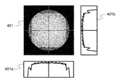
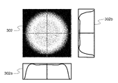
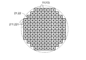
- FIG. 10 is a diagram showing the illuminance distribution at the position of the aperture stop in the illumination optical system of the comparative example; 2 is a diagram showing an illuminance distribution on an incident surface of an optical integrator in the illumination optical system shown in FIG. 1; FIG. 2 is a diagram showing an illuminance distribution at the position of an aperture stop in the illumination optical system shown in FIG. 1; FIG. FIG. 10 is a diagram showing a first modification regarding the arrangement of light emitting elements, condenser lenses, and lens elements; FIG. 10 is a diagram showing a second modification regarding the arrangement of light emitting elements, condenser lenses, and lens elements; It is a figure which shows the modification from which the structure of a lens array differs. FIG.
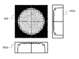
- FIG. 10 is a diagram showing a modified example in which the distance between the relay optical system and the optical integrator is different; 14 is a diagram showing the illuminance distribution on the incident surface of the optical integrator in the illumination optical system shown in FIG. 13; FIG. 14 is a diagram showing the illuminance distribution at the position of the aperture stop in the illumination optical system shown in FIG. 13; FIG.
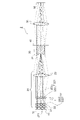
- FIG. 1 is a diagram showing one embodiment of the illumination optical system of the present invention.
- the illumination optical system 1 shown in FIG. 1 is an optical system that irradiates the mask M with light.
- a pattern is formed on the mask M to transmit the irradiated light, and the mask M is arranged on the surface to be irradiated.
- the illumination optical system 1 includes a light source 10, a relay optical system 20, an optical integrator 30, an aperture stop 40, and a condenser lens 50.
- the optical axis AX of the illumination optical system 1 is oriented vertically in the figure.
- the direction of the optical axis AX is used as a reference, the direction along the optical axis AX may be referred to as the Z direction, and the two-dimensional direction perpendicular to the optical axis AX may be referred to as the XY direction.
- the light source 10 has a plurality of light emitting elements 11, and LEDs are used as the light emitting elements 11, for example.
- the light-emitting element 11 emits light from its light-emitting surface, and is not limited to an LED.
- the light-emitting element 11 may emit light from a light-emitting surface, for example, by guiding light from a semiconductor laser through an optical fiber or the like.
- the relay optical system 20 superimposes the light emitted from each light emitting element 11 of the light source 10 and guides it to the incident surface 31 of the optical integrator 30 .
- the detailed structure and action of the relay optical system 20 will be described later.
- the optical integrator 30 divides the wavefront of light incident on the incident surface 31 by a plurality of wavefront dividing elements 32 and transmits the wavefront to the output surface 33 side. Note that the number of wavefront splitting elements 32 in the optical integrator 30 does not depend on the number of light emitting elements 11 in the light source 10 .
- the aperture stop 40 narrows down the light emitted from the emission surface 33 of the optical integrator 30 .
- the aperture stop 40 may be openable and closable, but the aperture stop 40 in this embodiment has a fixed aperture diameter that matches the fineness of the pattern formed on the mask M (whether it is a coarse pattern or a fine pattern).
- the size of the aperture diaphragm 40 corresponds to the NA (numerical aperture) of the illumination optical system, and the size of the aperture diaphragm 40 and the illuminance distribution on the plane of the aperture diaphragm are related to the NA of the projection optical system to determine the resolution for each pattern size of the exposure. Affects performance.
- the condenser lens 50 corresponds to an example of the condenser optical system according to the present invention, and irradiates the surface to be irradiated (that is, the mask M) with the light that has passed through the aperture stop 40 .
- Condenser lens 50 may be a combination lens in which a plurality of lenses are combined.
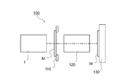
- FIG. 2 is a diagram showing an embodiment of the exposure apparatus of the present invention.
- the exposure apparatus 100 includes an illumination optical system 1 , a mask stage 110 , a projection optical system 120 and a work stage 130 .
- a mask stage 110 holds a mask M, and the illumination optical system 1 irradiates the mask M with light.
- the work stage 130 holds a work W to be exposed, such as a glass substrate or a semiconductor substrate.
- the projection optical system 120 projects the light transmitted through the mask M onto the work W to expose the work W in a pattern.
- the exposure apparatus 100 may be of a type in which the workpiece W is held close to or in contact with the mask M without having the projection optical system 120 .
- the relay optical system 20 has a condenser lens group 21, a lens array 22, and a relay lens 23, for example.
- the condenser lens group 21 has a plurality of condenser lenses 211 corresponding to the plurality of light emitting elements 11 of the light source 10, and the lens array 22 has a plurality of lens elements 221 corresponding to the plurality of condenser lenses 211.
- the condenser lens 211 of the condenser lens group 21 corresponds to an example of the first lens element according to the invention
- the lens element 221 of the lens array 22 corresponds to an example of the second lens element according to the invention.
- Each condensing lens 211 converges the light emitted from each corresponding light emitting element 11 on the incident side of the corresponding lens element 221 .
- the parallel light flux component of the light emitted from the light emitting element 11 is condensed by the condensing lens 211 at a location corresponding to the direction of the parallel light flux.
- the divergent light flux component emitted from one point on the light emitting element 11 is incident on the lens element 221 by the condensing lens 211 as a parallel light flux or as a light flux at an angle close to the parallel light flux.
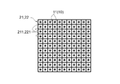
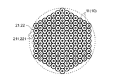
- FIG. 3 is a diagram showing the positional relationship among the light emitting element 11, the condenser lens 211, and the lens element 221. As shown in FIG.
- FIG. 3 shows the positional relationship among the light emitting element 11, the condenser lens 211, and the lens element 221 when the light source 10, the condenser lens group 21, and the lens array 22 are viewed in the Z direction.
- the positional relationship shown in FIG. 3 is the positional relationship when the irradiation shape on the mask M (surface) is square.
- a plurality of light emitting elements 11 are arranged in the XY directions, and each light emitting element 11 has a square light emitting surface.
- Each condensing lens 211 and each lens element 221 are arranged corresponding to each light emitting element 11 .
- the condenser lens 211 has a square outer shape, and the condenser lens group 21 is formed by bundling the square condenser lenses 211 in the XY directions.
- the outer shape of the lens elements 221 is rectangular, and the lens array 22 is formed by bundling the rectangular lens elements 221 in the XY directions.
- the condensing lens group 21 and the lens array 22 also have a rectangular outer shape.
- the condenser lens 211 corresponds to an example of the first lens element of the present invention, and the first lens element of the present invention may have a round outer shape. According to the condensing lens group 21 in which the lenses 211 are bundled, the light emitted from each light emitting element 11 of the light source 10 is efficiently condensed, so that the light utilization efficiency is high.
- the lens element 221 corresponds to an example of the second lens element according to the present invention, and the second lens element according to the present invention may have a round outer shape.
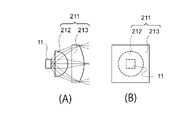
- the condenser lens 211 of the condenser lens group 21 may be a so-called single lens shown in FIG. 1, or may be a combination lens of, for example, two lenses.
- FIG. 4 is a diagram showing the condenser lens 211 of the combination lens.
- FIG. 4 shows a side view (A) and a front view (B).
- a condenser lens 211 of a combined lens is formed by combining a front lens 212 on the side of the light emitting element 11 and a rear lens 213 on the side of the lens array 22 .
- the front lens 212 has a round profile and the rear lens 213 has a square profile.
- the condenser lens 211 is a combination lens, the combination of the round front lens 212 and the square rear lens 213 improves the light utilization efficiency.
- the front lens 212 corresponds to an example of the front element according to the invention
- the rear lens 213 corresponds to an example of the rear element according to the invention. 4 is combined with the lens array 22 shown in FIG.
- the condenser lens group 21 consisting of the condenser lenses 211 shown in FIG. It is expected that the light utilization efficiency is improved by about 10% compared to the case where the array 22 is not combined (comparative example to be described later). Returning to FIG. 1 again, the description is continued.
- the relay lens 23 superimposes the light emitted from each lens element 221 of the lens array 22 and causes the light to enter the incident surface 31 of the optical integrator 30 .
- the divergent light flux component emitted from one point on the output side of the lens array 22 is incident on the incident surface 31 of the optical integrator 30 as a parallel light flux or a light flux at an angle close to the parallel light flux, and is then emitted from the lens array 22.
- the emitted parallel light beam component or the component with an angle close to the parallel light beam is condensed at the center on the incident surface 31 of the optical integrator 30 .
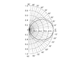
- FIG. 5 is a diagram showing the light distribution characteristics of the light emitting element 11. As shown in FIG.
- FIG. 5 shows polar coordinates with the Z direction at 0°, and the light distribution characteristic of the light emitting element 11 is represented by a solid line.
- the light distribution characteristic indicated by the dotted line in FIG. 5 is the light distribution characteristic when the light source is Lambertian light distribution. Both the solid line and the dotted line are indicated by relative values with the 0° direction set to 1. Compared to the Lambertian light distribution indicated by the dotted line, the light-emitting element 11 has a weaker luminous flux with respect to a large angle, and a smaller value. The luminous flux becomes stronger at the angle.
- each lens element 221 of the lens array 22 is irradiated with the light in the range of -50° to +50° captured by the lens element 211 among the light corresponding to the light distribution characteristics.
- the lens element 221 has a square outer shape
- the light illuminating the incident surface of the lens element 221 has a wider range than the inscribed circle of the square, but the light superimposed on the incident surface 31 of the optical integrator 30 has a shape close to a circle.
- the mask M on the surface to be irradiated is irradiated with the light with high utilization efficiency.
- the illuminance distribution in the embodiment shown in FIG. 1 will be described in comparison with a comparative example.
- FIG. 6 is a diagram showing the illuminance distribution on the incident surface 31 of the optical integrator 30 in the illumination optical system of the comparative example
- FIG. 7 is a diagram showing the illuminance distribution at the position of the aperture stop 40 in the illumination optical system of the comparative example. be.
- FIGS. 6 and 7 show illuminance distribution diagrams 301 and 401 showing two-dimensional illuminance distributions in the XY directions, and illuminance distribution diagrams 301 and 401 on straight lines in the X direction (horizontal direction in the figures) passing through the centers of the illuminance distribution diagrams 301 and 401.
- Illuminance graphs 301a and 401a showing the distributions
- illuminance graphs 301b and 401b showing the illuminance distributions on straight lines in the Y direction (vertical direction in the drawing) passing through the centers of the illuminance distribution diagrams 301 and 401 are shown. (This is the same for illuminance distribution diagrams below.)
- the incident surface 31 of the optical integrator 30 is irradiated with light in a square shape.
- the illuminance distribution is nearly uniform within the range irradiated with light.
- the illuminance distribution in the comparative example is an illuminance distribution designed to maximize the light utilization efficiency on the surface to be illuminated.
- the total amount of light on the entire incident surface 31 of the optical integrator 30 is 756.2 as a relative value based on the amount of light emitted from the light source 10 .
- the total amount of light passing through the aperture stop 40 is 507.0 as the above relative value.
- the illuminance of the light passing through the aperture stop 40 is greatly reduced in the peripheral portions in the vertical and horizontal directions. For fine patterns, it is better to design the illumination range to be wide so that the illumination intensity in this area does not decrease. In this case, the amount of light blocked by the aperture stop 40 increases, and the total amount of light becomes 454.1 in terms of the above relative value, further lowering the light utilization efficiency.
- FIG. 8 is a diagram showing the illuminance distribution on the incident surface 31 of the optical integrator 30 in the illumination optical system 1 shown in FIG. 1.
- FIG. 9 is a diagram showing the illuminance distribution at the position of the aperture stop 40 in the illumination optical system 1 shown in FIG. It is a figure which shows.
- the incident surface 31 of the optical integrator 30 is irradiated with light in a round shape. Further, as shown in the illuminance graphs 302a and 302b, the illuminance distribution is nearly uniform within the range irradiated with light, and the illuminance is slightly higher at the outer edge of the irradiated range. In the illumination optical system 1 of this embodiment, the total amount of light on the entire incident surface 31 of the optical integrator 30 is 729.2 as the above relative value.
- the illumination optical system 1 of the first embodiment the total amount of light passing through the aperture stop 40 is 558.1 in terms of the above relative value, which is higher than the comparative example shown in FIGS. 6 and 7 .
- modified examples of the illumination optical system 1 of this embodiment will be described. 10 and 11 are diagrams showing modifications regarding the arrangement of the light emitting element 11, the condenser lens 211, and the lens element 221, and are examples in which the irradiation shape on the mask M (surface) is circular.
- the light emitting elements 11 of the light source 10 are arranged vertically and horizontally within a circular area indicated by dotted lines.
- the condensing lens 211 and the lens element 221 each have a square outer shape, and each condensing lens 211 and each lens element 221 are arranged corresponding to each light emitting element 11.
- FIG. 10 Even with the circular arrangement shown in FIG. 10, the light utilization efficiency is improved by having each condensing lens 211 and each lens element 221 having a square outer shape.
- the light emitting elements 11 of the light source 10 are arranged in a hexagonal shape within the circular range indicated by the dotted line, and the array of the light emitting elements 11 is such that the rows in three directions different from each other by 60° intersect. It is an array. 11, the condensing lens 211 and the lens element 221 each have a round outer shape, and each condensing lens 211 and each lens element 221 are arranged corresponding to each light emitting element 11. be. It should be noted that each condenser lens 211 and lens element 221 may each have a hexagonal outer shape. In the modification in which each condensing lens 211 and each lens element 221 has a round outer shape, the light utilization efficiency is lower than the arrangement shown in FIGS.
- the irradiation range is designed to be wide on the incident surface of the optical integrator 30 so that the illumination distribution is flat to the periphery on the surface of the aperture diaphragm 40 in the comparative example shown in FIGS.
- Light utilization efficiency is higher than in the case of FIG. 12 is a diagram showing a modification in which the structure of the lens array 22 is different.
- each lens element 221 of the lens array 22 is composed of a first lens 222 and a second lens 223 . That is, the lens array 22 is composed of a pair of the lens array of the first lens 222 and the lens array of the second lens 223 .
- the weight of the lens array 22 can be reduced.
- the lens element 221 composed of a pair of the first lens 222 and the second lens 223 also corresponds to an example of the second lens element according to the invention.
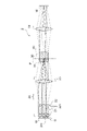
- FIG. 13 shows a modification in which the distance between the relay optical system 20 and the optical integrator 30 is different.
- the structures of the light source 10 and the relay optical system 20, and the structure from the optical integrator 30 to the condenser lens 50 are the same as those of the illumination optical system 1 shown in FIG.
- the distance from the relay optical system 20 to the incident surface 31 of the optical integrator 30 is different between the illumination optical system 3 of the modified example and the illumination optical system 1 shown in FIG.
- the distance in the modified illumination optical system 3 shown in FIG. 13 is shorter than the distance in the illumination optical system 1 shown in FIG.
- the light enters the incident surface 31 of the optical integrator 30 on a surface closer to the relay lens 23 with respect to the superimposing surface P on which the images are superimposed by the relay lens 23 of the relay optical system 20 .
- the illumination light enters the optical integrator 30 on a plane different from the superimposing plane P, but as a result, the light utilization efficiency is almost the same as when the light enters on the superimposing plane P.
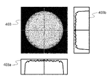
- FIG. 14 is a diagram showing the illuminance distribution on the incident surface 31 of the optical integrator 30 in the illumination optical system 3 shown in FIG. 13, and FIG. 15 shows the illuminance distribution at the position of the aperture stop 40 in the illumination optical system 3 shown in FIG. It is a figure which shows.
- the illumination optical system 3 of the modified example shown in FIG. As shown in the illuminance distribution diagram 303 of FIG. 14, the illumination optical system 3 of the modified example shown in FIG. Also, as shown in the illuminance graphs 303a and 303b, the illuminance distribution is nearly uniform within the range irradiated with light. Illumination optical system 3 shown in FIG. 13 has better uniformity of illuminance distribution than illumination optical system 1 shown in FIG. is 729.1 as the above relative value.
- the light passes through the entire opening of the aperture stop 40 as shown in the illuminance distribution diagram 403 of FIG. Further, as shown in the illuminance graphs 403a and 403b in FIG. 15, the light passing through the aperture stop 40 has a more uniform illuminance distribution within the range of the aperture. As a result, in the illumination optical system 3 shown in FIG. 13, the total amount of light passing through the aperture stop 40 is 563.5 in terms of the above relative value, and the light utilization efficiency is equal to that of the optical integrator 30 shown in the illumination optical system 1 in FIG.
- the illumination intensity distribution can be uniform to the periphery on the surface of the aperture stop 40 without reducing the illumination intensity, making it suitable for exposure of finer patterns. It is superior to the comparative example shown in FIG. 7 and the examples shown in FIGS.
- the incident surface of the optical integrator 30 is arranged so that the distance from the relay lens 23 is long with respect to the superimposed plane P. I don't mind.
- the illumination optical system of the present invention may be applied to an exposure apparatus that uniformly exposes the entire surface of an exposure target. , may be applied to illumination other than exposure.
Landscapes
- Physics & Mathematics (AREA)
- General Physics & Mathematics (AREA)
- Optics & Photonics (AREA)
- Engineering & Computer Science (AREA)
- General Engineering & Computer Science (AREA)
- Microelectronics & Electronic Packaging (AREA)
- Exposure And Positioning Against Photoresist Photosensitive Materials (AREA)
- Microscoopes, Condenser (AREA)
- Exposure Of Semiconductors, Excluding Electron Or Ion Beam Exposure (AREA)
Abstract
Description
そこで、本発明は、複数の発光素子からの光を高い効率で利用することを目的とする。
集光レンズ群、レンズアレイ、およびリレーレンズによりリレー光学系の機能が分担され、リレー光学系が容易に実現される。
上記露光装置において、上記照明光学系によって照射された前記パターンの像を上記露光対象物に投影する投影光学系を備えてもよい。
図1は、本発明の照明光学系の一実施形態を示す図である。
図2は、本発明の露光装置の一実施形態を示す図である。
露光装置100には、照明光学系1と、マスクステージ110と、投影光学系120と、ワークステージ130が備えられている。
マスクステージ110はマスクMを保持し、そのマスクMには照明光学系1によって光が照射される。
ワークステージ130には、例えばガラス基板や半導体基板などといった露光対象となるワークWが保持される。
投影光学系120は、マスクMを透過した光をワークW上に投影してワークWをパターン露光する。
露光装置100は、投影光学系120を有さずに、ワークWがマスクMに近接あるいは接触して保持される方式のものであってもよい。
図1に戻って、リレー光学系20の詳細について説明する。
リレー光学系20は、一例として、集光レンズ群21と、レンズアレイ22と、リレーレンズ23とを有する。
図3は、発光素子11と集光レンズ211とレンズ要素221との位置関係を示す図である。
複数の発光素子11はXY方向に配列されており、各発光素子11は四角い発光面を有している。
集光レンズ群21の集光レンズ211は、図1に示すいわゆる単玉レンズであってもよいが、例えば2枚のレンズによる組み合わせレンズであってもよい。
図4は、組み合わせレンズの集光レンズ211を示す図である。
図4には、側面図(A)と正面図(B)が示されている。
図4に示す集光レンズ211からなる集光レンズ群21が図3に示すレンズアレイ22と組み合わされることにより、図4に示す集光レンズ211からなる集光レンズ群21が図3に示すレンズアレイ22と組み合わされない場合(後述する比較例)と比較して光の利用効率が10%程度向上することが期待される。
再び図1に戻って説明を続ける。
図5は、発光素子11の配光特性を示す図である。
ここで、図1に示す実施形態における照度分布を比較例と比較して説明する。
比較例における照度分布は、被照射面において光の利用効率が最も良くなるよう設計された場合の照度分布である。
オプティカルインテグレータ30の入射面31全体での合計光量は、光源10における発光量を基準とした相対値で756.2となっている。
次に、本実施形態の照明光学系1に対する変形例について説明する。
図10および図11は、発光素子11、集光レンズ211、およびレンズ要素221の配置に関する変形例を示す図であり、マスクM(面)での照射形状が円形である場合の例である。
図10に示す丸い配置であっても、各集光レンズ211および各レンズ要素221が四角い外形を有することで光の利用効率が向上する。
各集光レンズ211および各レンズ要素221が丸い外形を有する変形例では、図3および図10に示す配置と較べると光の利用効率が低いが、発光素子11を点線で示した丸い範囲内に多く配置できる。また開口絞り40面でフラットな照度分布になるため図6、図7の比較例で開口絞り40の面で周辺までフラットな照度分布になるようにオプティカルインテグレータ30の入射面で照射範囲を広く設計した場合と比較すると光の利用効率が高くなる。
図12は、レンズアレイ22の構造が異なる変形例を示す図である。
図13は、リレー光学系20とオプティカルインテグレータ30との距離が異なる変形例を示す図である。
21…集光レンズ群、211…集光レンズ、212…前レンズ、213…後レンズ
22…レンズアレイ、221…レンズ要素、23…リレーレンズ、
30…オプティカルインテグレータ、31…入射面、32…波面分割要素、33…出射面
40…開口絞り、50…コンデンサレンズ、100…露光装置、
110…マスクステージ、120…投影光学系、130…ワークステージ
Claims (8)
- 各々が発光面から光を発する複数の発光素子が、当該発光面の広がる方向に互いに並んでいる光源と、
前記発光素子が発した光の配光分布を照度分布に変換すると共に、前記複数の発光素子に対応した複数の当該照度分布を重畳面上で互いに重ね合わせるリレー光学系と、
前記リレー光学系による照射光を波面分割して複数の光束として伝達する複数の波面分割要素が互いに並列的に配置されたオプティカルインテグレータと、
前記複数の光束を被照射面で重畳させるコンデンサ光学系と、
を備えたことを特徴とする照明光学系。 - 前記リレー光学系が、
前記複数の発光素子に対応した複数の第1レンズ要素を有し、各第1レンズが各発光素子からの光を集光する集光レンズ群と、
前記複数の第1レンズ要素に対応した複数の第2レンズ要素を有し、各発光素子からの光の配光分布に相当する照度分布の照射光が各第1レンズにより各第2レンズ要素の入射面に照射されるレンズアレイと、
前記レンズアレイの各第2レンズ要素の出射面と光学的に協働して、各第2レンズ要素の入射面に照射された各照射光を前記重畳面上に導いて互いに重ね合わせるリレーレンズと、
を備えたことを特徴とする請求項1に記載の照明光学系。 - 前記リレーレンズから前記オプティカルインテグレータの入射面までの距離は、当該リレーレンズから前記重畳面までの距離よりも短いことを特徴とする請求項2に記載の照明光学系。
- 前記レンズアレイは、前記複数の第2レンズ要素のそれぞれが、光軸に沿った方向に見て四角形の外形を有し、当該複数の第2レンズ要素が束ねられたことを特徴とする請求項2または3に記載の照明光学系。
- 前記集光レンズ群は、前記複数の第1レンズ要素のそれぞれの出射側が、光軸に沿った方向に見て四角形の外形を有し、当該複数の第1レンズ要素が束ねられたことを特徴とする請求項2または3に記載の照明光学系。
- 前記集光レンズ群は、前記複数の第1レンズ要素のそれぞれが、前記発光素子側に位置する前要素と前記レンズアレイ側に位置する後要素とを有し、当該前要素は光軸に沿った方向に見て丸い外形を有し、当該後要素は光軸に沿った方向に見て四角形の外形を有することを特徴とする請求項5に記載の照明光学系。
- 請求項1または2に記載の照明光学系で前記被照射面に配置されたパターンを照射して、当該パターンを露光対象物に露光することを特徴とする露光装置。
- 前記照明光学系によって照射された前記パターンの像を前記露光対象物に投影する投影光学系を備えたことを特徴とする請求項7に記載の露光装置。
Priority Applications (4)
| Application Number | Priority Date | Filing Date | Title |
|---|---|---|---|
| KR1020237043662A KR102951745B1 (ko) | 2021-07-08 | 2022-03-24 | 조명 광학계 및 노광 장치 |
| US18/575,358 US12481220B2 (en) | 2021-07-08 | 2022-03-24 | Lighting optical system and exposure apparatus |
| CN202280042886.9A CN117501183A (zh) | 2021-07-08 | 2022-03-24 | 照明光学系统及曝光装置 |
| EP22837272.8A EP4361701A4 (en) | 2021-07-08 | 2022-03-24 | OPTICAL ILLUMINATION SYSTEM AND EXPOSURE DEVICE |
Applications Claiming Priority (2)
| Application Number | Priority Date | Filing Date | Title |
|---|---|---|---|
| JP2021113402A JP7677004B2 (ja) | 2021-07-08 | 2021-07-08 | 照明光学系および露光装置 |
| JP2021-113402 | 2021-07-08 |
Publications (1)
| Publication Number | Publication Date |
|---|---|
| WO2023281850A1 true WO2023281850A1 (ja) | 2023-01-12 |
Family
ID=84801657
Family Applications (1)
| Application Number | Title | Priority Date | Filing Date |
|---|---|---|---|
| PCT/JP2022/013874 Ceased WO2023281850A1 (ja) | 2021-07-08 | 2022-03-24 | 照明光学系および露光装置 |
Country Status (7)
| Country | Link |
|---|---|
| US (1) | US12481220B2 (ja) |
| EP (1) | EP4361701A4 (ja) |
| JP (1) | JP7677004B2 (ja) |
| KR (1) | KR102951745B1 (ja) |
| CN (1) | CN117501183A (ja) |
| TW (1) | TWI905419B (ja) |
| WO (1) | WO2023281850A1 (ja) |
Cited By (1)
| Publication number | Priority date | Publication date | Assignee | Title |
|---|---|---|---|---|
| EP4617772A1 (en) * | 2024-03-11 | 2025-09-17 | Ushio Denki Kabushiki Kaisha | Light source device |
Citations (5)
| Publication number | Priority date | Publication date | Assignee | Title |
|---|---|---|---|---|
| JP2001147305A (ja) * | 1999-11-19 | 2001-05-29 | Seiko Epson Corp | マイクロレンズ用凹部付き基板の製造方法、マイクロレンズ基板、液晶パネル用対向基板、液晶パネルおよび投射型表示装置 |
| JP2003107400A (ja) * | 2001-07-26 | 2003-04-09 | Ricoh Co Ltd | 画像表示装置 |
| JP2007025613A (ja) * | 2004-09-03 | 2007-02-01 | Sanee Giken Kk | 露光用光源 |
| JP2016188878A (ja) | 2015-03-28 | 2016-11-04 | 株式会社ニコン | 照明光学系、露光装置、およびデバイス製造方法 |
| JP2020122921A (ja) * | 2019-01-31 | 2020-08-13 | キヤノン株式会社 | 光源装置、照明装置、露光装置及び物品の製造方法 |
Family Cites Families (14)
| Publication number | Priority date | Publication date | Assignee | Title |
|---|---|---|---|---|
| US5815248A (en) * | 1993-04-22 | 1998-09-29 | Nikon Corporation | Illumination optical apparatus and method having a wavefront splitter and an optical integrator |
| US5822125A (en) * | 1996-12-20 | 1998-10-13 | Eastman Kodak Company | Lenslet array system |
| JP3101613B2 (ja) * | 1998-01-30 | 2000-10-23 | キヤノン株式会社 | 照明光学装置及び投影露光装置 |
| JP3599629B2 (ja) * | 2000-03-06 | 2004-12-08 | キヤノン株式会社 | 照明光学系及び前記照明光学系を用いた露光装置 |
| WO2011012148A1 (en) * | 2009-07-31 | 2011-02-03 | Carl Zeiss Smt Gmbh | Optical beam deflecting element and method of adjustment |
| JP2011216863A (ja) * | 2010-03-17 | 2011-10-27 | Hitachi Via Mechanics Ltd | ビームサイズ可変照明光学装置及びビームサイズ変更方法 |
| TWI519824B (zh) * | 2011-03-25 | 2016-02-01 | 銘異科技股份有限公司 | 混光方法、混光裝置以及應用該混光裝置之小型投影系統 |
| JP2014003086A (ja) * | 2012-06-15 | 2014-01-09 | Ushio Inc | 光照射装置、露光装置 |
| CN102854632A (zh) * | 2012-08-16 | 2013-01-02 | 芜湖雅图数字视频技术有限公司 | 激光光源准直装置、准直装置阵列及照明系统和投影设备 |
| KR101633176B1 (ko) | 2014-05-14 | 2016-07-01 | 주은유브이텍 주식회사 | 자외선 엘이디 모듈 및 이를 포함하는 자외선 노광장치 |
| CN107885038A (zh) * | 2016-09-30 | 2018-04-06 | 上海微电子装备(集团)股份有限公司 | 照明均匀性校正装置、校正方法以及一种曝光投影系统 |
| KR102036749B1 (ko) | 2017-12-14 | 2019-10-28 | 에스엘 주식회사 | 차량용 램프 |
| JP7508278B2 (ja) * | 2020-06-04 | 2024-07-01 | キヤノン株式会社 | 露光装置、露光方法、及び物品の製造方法 |
| JP2024172758A (ja) * | 2023-06-01 | 2024-12-12 | ウシオ電機株式会社 | 照明光学系、露光装置、照射方法、及び部品の製造方法 |
-
2021
- 2021-07-08 JP JP2021113402A patent/JP7677004B2/ja active Active
-
2022
- 2022-03-24 WO PCT/JP2022/013874 patent/WO2023281850A1/ja not_active Ceased
- 2022-03-24 US US18/575,358 patent/US12481220B2/en active Active
- 2022-03-24 CN CN202280042886.9A patent/CN117501183A/zh active Pending
- 2022-03-24 EP EP22837272.8A patent/EP4361701A4/en active Pending
- 2022-03-24 KR KR1020237043662A patent/KR102951745B1/ko active Active
- 2022-04-19 TW TW111114811A patent/TWI905419B/zh active
Patent Citations (5)
| Publication number | Priority date | Publication date | Assignee | Title |
|---|---|---|---|---|
| JP2001147305A (ja) * | 1999-11-19 | 2001-05-29 | Seiko Epson Corp | マイクロレンズ用凹部付き基板の製造方法、マイクロレンズ基板、液晶パネル用対向基板、液晶パネルおよび投射型表示装置 |
| JP2003107400A (ja) * | 2001-07-26 | 2003-04-09 | Ricoh Co Ltd | 画像表示装置 |
| JP2007025613A (ja) * | 2004-09-03 | 2007-02-01 | Sanee Giken Kk | 露光用光源 |
| JP2016188878A (ja) | 2015-03-28 | 2016-11-04 | 株式会社ニコン | 照明光学系、露光装置、およびデバイス製造方法 |
| JP2020122921A (ja) * | 2019-01-31 | 2020-08-13 | キヤノン株式会社 | 光源装置、照明装置、露光装置及び物品の製造方法 |
Non-Patent Citations (1)
| Title |
|---|
| See also references of EP4361701A4 |
Cited By (2)
| Publication number | Priority date | Publication date | Assignee | Title |
|---|---|---|---|---|
| EP4617772A1 (en) * | 2024-03-11 | 2025-09-17 | Ushio Denki Kabushiki Kaisha | Light source device |
| US12595894B2 (en) | 2024-03-11 | 2026-04-07 | Ushio Denki Kabushiki Kaisha | Light source device with fly-eye integrator |
Also Published As
| Publication number | Publication date |
|---|---|
| JP7677004B2 (ja) | 2025-05-15 |
| JP2023009810A (ja) | 2023-01-20 |
| KR20240010018A (ko) | 2024-01-23 |
| KR102951745B1 (ko) | 2026-04-14 |
| EP4361701A4 (en) | 2024-11-06 |
| TW202303219A (zh) | 2023-01-16 |
| US12481220B2 (en) | 2025-11-25 |
| US20240319610A1 (en) | 2024-09-26 |
| TWI905419B (zh) | 2025-11-21 |
| EP4361701A1 (en) | 2024-05-01 |
| CN117501183A (zh) | 2024-02-02 |
Similar Documents
| Publication | Publication Date | Title |
|---|---|---|
| TWI392897B (zh) | 微型光學透鏡、含此透鏡之發光二極體封裝結構、及微型光學透鏡角度的設計方法 | |
| JP4059623B2 (ja) | 照明装置、及び均一照明装置 | |
| JP4670876B2 (ja) | 照明光学系および画像表示装置 | |
| EP3541069B1 (en) | Illumination unit | |
| JP2011128634A (ja) | 照明光学系および画像表示装置 | |
| JP6172540B2 (ja) | 光源装置 | |
| CN112815272B (zh) | 光源系统和发光设备 | |
| KR20110092215A (ko) | 광 조사 장치 | |
| JP6806236B2 (ja) | 照明装置及び方法、露光装置及び方法、並びにデバイス製造方法 | |
| WO2023281850A1 (ja) | 照明光学系および露光装置 | |
| JP2009151313A (ja) | 面を照明する装置、ならびに作業領域に光を作用させる装置 | |
| CN107728433B (zh) | 曝光照明装置 | |
| JP2008249454A (ja) | 照明光学装置および試料検査装置 | |
| JP2006133635A (ja) | 照明光学装置及び光学装置 | |
| WO2017138523A1 (ja) | 光源装置 | |
| WO2016152359A1 (ja) | 光源装置、露光装置 | |
| JP5843905B2 (ja) | 照明光学系、露光装置及びデバイス製造方法 | |
| CN114764186A (zh) | 用于成像应用的自适应照明系统 | |
| US20070058149A1 (en) | Lighting system and exposure apparatus | |
| CN220338298U (zh) | 照明装置 | |
| WO2025204599A1 (ja) | 光源装置 | |
| JP7068659B2 (ja) | 露光用光源装置 | |
| WO2023106113A1 (ja) | 検査システム及び検査用スポット照明装置 | |
| WO2020116081A1 (ja) | 露光用光源装置 | |
| KR20170121570A (ko) | 조명장치 |
Legal Events
| Date | Code | Title | Description |
|---|---|---|---|
| 121 | Ep: the epo has been informed by wipo that ep was designated in this application |
Ref document number: 22837272 Country of ref document: EP Kind code of ref document: A1 |
|
| WWE | Wipo information: entry into national phase |
Ref document number: 202280042886.9 Country of ref document: CN |
|
| ENP | Entry into the national phase |
Ref document number: 20237043662 Country of ref document: KR Kind code of ref document: A |
|
| WWE | Wipo information: entry into national phase |
Ref document number: 1020237043662 Country of ref document: KR |
|
| WWE | Wipo information: entry into national phase |
Ref document number: 18575358 Country of ref document: US |
|
| WWE | Wipo information: entry into national phase |
Ref document number: 2022837272 Country of ref document: EP |
|
| ENP | Entry into the national phase |
Ref document number: 2022837272 Country of ref document: EP Effective date: 20240122 |
|
| NENP | Non-entry into the national phase |
Ref country code: DE |
|
| WWG | Wipo information: grant in national office |
Ref document number: 18575358 Country of ref document: US |