WO2024024497A1 - Dispositif de stockage, appareil électronique, et procédé de commande de dispositif de stockage - Google Patents
Dispositif de stockage, appareil électronique, et procédé de commande de dispositif de stockage Download PDFInfo
- Publication number
- WO2024024497A1 WO2024024497A1 PCT/JP2023/025590 JP2023025590W WO2024024497A1 WO 2024024497 A1 WO2024024497 A1 WO 2024024497A1 JP 2023025590 W JP2023025590 W JP 2023025590W WO 2024024497 A1 WO2024024497 A1 WO 2024024497A1
- Authority
- WO
- WIPO (PCT)
- Prior art keywords
- layer
- magnetoresistive
- storage device
- storage
- resistance
- Prior art date
- Legal status (The legal status is an assumption and is not a legal conclusion. Google has not performed a legal analysis and makes no representation as to the accuracy of the status listed.)
- Ceased
Links
Images




Classifications
-
- G—PHYSICS
- G11—INFORMATION STORAGE
- G11B—INFORMATION STORAGE BASED ON RELATIVE MOVEMENT BETWEEN RECORD CARRIER AND TRANSDUCER
- G11B5/00—Recording by magnetisation or demagnetisation of a record carrier; Reproducing by magnetic means; Record carriers therefor
- G11B5/127—Structure or manufacture of heads, e.g. inductive
- G11B5/33—Structure or manufacture of flux-sensitive heads, i.e. for reproduction only; Combination of such heads with means for recording or erasing only
- G11B5/39—Structure or manufacture of flux-sensitive heads, i.e. for reproduction only; Combination of such heads with means for recording or erasing only using magneto-resistive devices or effects
-
- G—PHYSICS
- G11—INFORMATION STORAGE
- G11C—STATIC STORES
- G11C11/00—Digital stores characterised by the use of particular electric or magnetic storage elements; Storage elements therefor
- G11C11/02—Digital stores characterised by the use of particular electric or magnetic storage elements; Storage elements therefor using magnetic elements
- G11C11/16—Digital stores characterised by the use of particular electric or magnetic storage elements; Storage elements therefor using magnetic elements using elements in which the storage effect is based on magnetic spin effect
-
- G—PHYSICS
- G11—INFORMATION STORAGE
- G11C—STATIC STORES
- G11C11/00—Digital stores characterised by the use of particular electric or magnetic storage elements; Storage elements therefor
- G11C11/02—Digital stores characterised by the use of particular electric or magnetic storage elements; Storage elements therefor using magnetic elements
- G11C11/16—Digital stores characterised by the use of particular electric or magnetic storage elements; Storage elements therefor using magnetic elements using elements in which the storage effect is based on magnetic spin effect
- G11C11/161—Digital stores characterised by the use of particular electric or magnetic storage elements; Storage elements therefor using magnetic elements using elements in which the storage effect is based on magnetic spin effect details concerning the memory cell structure, e.g. the layers of the ferromagnetic memory cell
-
- G—PHYSICS
- G11—INFORMATION STORAGE
- G11C—STATIC STORES
- G11C11/00—Digital stores characterised by the use of particular electric or magnetic storage elements; Storage elements therefor
- G11C11/02—Digital stores characterised by the use of particular electric or magnetic storage elements; Storage elements therefor using magnetic elements
- G11C11/16—Digital stores characterised by the use of particular electric or magnetic storage elements; Storage elements therefor using magnetic elements using elements in which the storage effect is based on magnetic spin effect
- G11C11/165—Auxiliary circuits
- G11C11/1659—Cell access
-
- G—PHYSICS
- G11—INFORMATION STORAGE
- G11C—STATIC STORES
- G11C11/00—Digital stores characterised by the use of particular electric or magnetic storage elements; Storage elements therefor
- G11C11/02—Digital stores characterised by the use of particular electric or magnetic storage elements; Storage elements therefor using magnetic elements
- G11C11/16—Digital stores characterised by the use of particular electric or magnetic storage elements; Storage elements therefor using magnetic elements using elements in which the storage effect is based on magnetic spin effect
- G11C11/165—Auxiliary circuits
- G11C11/1673—Reading or sensing circuits or methods
-
- G—PHYSICS
- G11—INFORMATION STORAGE
- G11C—STATIC STORES
- G11C11/00—Digital stores characterised by the use of particular electric or magnetic storage elements; Storage elements therefor
- G11C11/02—Digital stores characterised by the use of particular electric or magnetic storage elements; Storage elements therefor using magnetic elements
- G11C11/16—Digital stores characterised by the use of particular electric or magnetic storage elements; Storage elements therefor using magnetic elements using elements in which the storage effect is based on magnetic spin effect
- G11C11/165—Auxiliary circuits
- G11C11/1675—Writing or programming circuits or methods
-
- G—PHYSICS
- G11—INFORMATION STORAGE
- G11C—STATIC STORES
- G11C11/00—Digital stores characterised by the use of particular electric or magnetic storage elements; Storage elements therefor
- G11C11/56—Digital stores characterised by the use of particular electric or magnetic storage elements; Storage elements therefor using storage elements with more than two stable states represented by steps, e.g. of voltage, current, phase, frequency
-
- H—ELECTRICITY
- H10—SEMICONDUCTOR DEVICES; ELECTRIC SOLID-STATE DEVICES NOT OTHERWISE PROVIDED FOR
- H10B—ELECTRONIC MEMORY DEVICES
- H10B61/00—Magnetic memory devices, e.g. magnetoresistive RAM [MRAM] devices
-
- H—ELECTRICITY
- H10—SEMICONDUCTOR DEVICES; ELECTRIC SOLID-STATE DEVICES NOT OTHERWISE PROVIDED FOR
- H10D—INORGANIC ELECTRIC SEMICONDUCTOR DEVICES
- H10D48/00—Individual devices not covered by groups H10D1/00 - H10D44/00
- H10D48/40—Devices controlled by magnetic fields
-
- H—ELECTRICITY
- H10—SEMICONDUCTOR DEVICES; ELECTRIC SOLID-STATE DEVICES NOT OTHERWISE PROVIDED FOR
- H10N—ELECTRIC SOLID-STATE DEVICES NOT OTHERWISE PROVIDED FOR
- H10N50/00—Galvanomagnetic devices
- H10N50/10—Magnetoresistive devices
Definitions
- the present disclosure relates to a storage device, an electronic device, and a method for controlling a storage device.
- Magnetoresistive Random Access Memory uses a magnetoresistive element (magnetoresistive memory element) as a storage element, and as it maintains its state depending on the magnetization state of the ferromagnetic material, it remains unchanged even when the power is turned off. It has a non-volatile nature in which recorded data is retained.
- the basic structure of a magnetoresistive element is a sandwich structure in which a non-magnetic thin film of an insulator is sandwiched between two magnetic layers made of thin magnetic films. This structure is called a magnetic tunnel junction (MTJ).
- MTJ magnetic tunnel junction
- the magnetization of one of the two magnetic layers is fixed, and the magnetization of the other magnetic layer (storage layer) is controlled by an external field.
- a state in which the magnetizations of the fixed magnetization layer and the storage layer are parallel to each other is defined as state 0, and a state in which they are antiparallel is defined as state 1. In this way, by rewriting the parallel/antiparallel state of magnetization, the state (“0” or “1”) is stored in a non-volatile manner.
- the memory capacity cannot be said to be sufficient due to various factors such as usage conditions and situations, and an increase in the desired capacity, and further increases in memory capacity are desired. In other words, even at present, it is desired to increase memory capacity while saving space.
- the present disclosure provides a storage device, an electronic device, and a storage device control method that can increase memory capacity while saving space.
- a storage device includes a magnetoresistive storage element that changes into at least four distinguishable resistance states, and that changes the magnetization direction of the magnetoresistive storage element or applies a blow current to the magnetoresistive storage element. and a writing unit that changes the magnetoresistive memory element into the at least four distinguishable resistance states by applying a current to the magnetoresistive memory element.
- An electronic device includes a storage device that stores information, and the storage device includes a magnetoresistive storage element that changes into at least four distinguishable resistance states, and a magnetization direction of the magnetoresistive storage element. and a writing unit that changes the magnetoresistive storage element into the at least four distinguishable resistance states by changing the resistance state or passing a blow current through the magnetoresistive storage element.
- a method for controlling a storage device includes changing the magnetization direction of a magnetoresistive storage element that is variable into at least four distinguishable resistance states, and flowing a blow current through the magnetoresistive storage element. and changing the resistance state of the magnetoresistive storage element into the at least four distinguishable resistance states.
- FIG. 1 is a diagram illustrating a configuration example of a storage device according to an embodiment of the present disclosure.
- 1 is a diagram showing a first configuration example of a memory cell according to an embodiment of the present disclosure.
- FIG. FIG. 7 is a diagram illustrating a second configuration example of a memory cell according to an embodiment of the present disclosure.
- 1 is a diagram showing a first configuration example of a magnetoresistive element according to an embodiment of the present disclosure.
- FIG. FIG. 3 is a diagram illustrating a second configuration example of a magnetoresistive element according to an embodiment of the present disclosure.
- FIG. 2 is a diagram for explaining distinguishable resistance states of a magnetoresistive element according to an embodiment of the present disclosure.
- FIG. 1 is a diagram showing a first configuration example of a memory cell according to an embodiment of the present disclosure.
- FIG. FIG. 7 is a diagram illustrating a second configuration example of a memory cell according to an embodiment of the present disclosure.
- 1 is a diagram showing a
- FIG. 3 is a diagram illustrating multi-leveling based on distinguishable resistance states of a magnetoresistive element according to an embodiment of the present disclosure.
- FIG. 3 is a diagram for explaining quaternization based on the distinguishable resistance state of the magnetoresistive element according to the embodiment of the present disclosure.
- FIG. 3 is a diagram for explaining quinarization based on the identifiable resistance state of the magnetoresistive element according to the embodiment of the present disclosure.
- 1 is a diagram illustrating a configuration example of a read circuit and a write circuit according to an embodiment of the present disclosure.
- FIG. FIG. 2 is a diagram for explaining a first configuration example of a write circuit according to an embodiment of the present disclosure.
- FIG. 7 is a diagram for explaining a second configuration example of a write circuit according to an embodiment of the present disclosure.
- 1 is a diagram showing an example of the configuration of an imaging device. It is a figure showing an example of composition of a distance measuring device.
- FIG. 2 is a diagram showing an example of the appearance of a game device.
- 1 is a diagram showing an example of the configuration of a game device.
- One or more embodiments (including examples and modifications) described below can each be implemented independently. On the other hand, at least a portion of the plurality of embodiments described below may be implemented in combination with at least a portion of other embodiments as appropriate. These multiple embodiments may include novel features that are different from each other. Therefore, these multiple embodiments may contribute to solving mutually different objectives or problems, and may produce mutually different effects. Note that the effects in each embodiment are merely examples and are not limited, and other effects may be provided.
- Embodiment 1-1 Configuration example of storage device 1-2.
- Example of memory cell configuration 1-3 Configuration example of magnetoresistive element 1-4.
- Discernible resistance state of magnetoresistive element 1-5 Multi-leveling based on distinguishable resistance states of magnetoresistive elements 1-6.
- Specific example of multivalue 1-7 Configuration example and operation example of read circuit and write circuit 1-8.
- Other embodiments 3.
- FIG. 1 is a diagram showing a configuration example of a storage device 1 according to this embodiment. This storage device 1 is applied to, for example, an LSI (large scale integrated circuit).
- LSI large scale integrated circuit
- the memory device 1 includes a control circuit 5, a voltage generation circuit 6, a memory cell array 10, a word line control circuit 20, a bit line control circuit 30, and a sense amplifier 40. , a read circuit 50 , and a write circuit 60 .
- the read circuit 50 corresponds to a read section
- the write circuit 60 corresponds to a write section
- each of the control circuits 5, 20, and 30 corresponds to a control section.
- the control circuit 5 processes write/read instructions from an external circuit (for example, an arithmetic circuit) and controls data input/output. For example, the control circuit 5 receives a command (command for writing, reading, etc.) from an external circuit, and controls writing and reading of data based on the received command.
- an external circuit for example, an arithmetic circuit
- the arithmetic circuit may be, for example, a circuit that performs logical operations such as an AI (artificial intelligence) function, a recognition function, or machine learning.
- This arithmetic circuit performs various arithmetic processing based on a program, for example.
- programs, various setting values, and the like may be stored in the storage device 1 on a long-term basis, and data generated through arithmetic processing may be stored on a short-term basis in the storage device 1.
- the voltage generation circuit 6 generates a voltage used when writing and reading data to the memory cell array 10, and supplies the generated voltage to the write circuit 60 and the read circuit 50.
- the memory cell array 10 is composed of memory cells 100 that store data arranged in a two-dimensional matrix.
- the memory cell 100 includes a selection element 110 and a magnetoresistive element (magnetoresistive storage element) 120.
- a VC (Voltage Controlled)-MRAM cell can be used as the memory cell 100.
- the selection element 110 is an element that is connected to one end of the magnetoresistive element 120 and controls the application of voltage to the magnetoresistive element 120.
- an n-channel MOS transistor can be used.
- the magnetoresistive element 120 for example, a magnetoresistive element such as MTJ can be used.
- the magnetization direction can be changed between a first state and a second state by applying a voltage.
- External fields used to control the magnetization direction include a current magnetic field generated by passing current to external wiring, a method that applies current directly to the MTJ and utilizes the spin angular momentum transfer (STT) effect, and voltage.
- STT spin angular momentum transfer
- VCMA voltage controlled magnetic anisotropy
- TMR tunnel magneto-resistance
- the currently mainstream MRAM is STT-MRAM, which can be made smaller and consumes less power than when using a current magnetic field.
- voltage controlled (VC) MRAM using VCMA ie, VC-MRAM
- VC-MRAM voltage controlled MRAM using VCMA
- This VC-MRAM is nonvolatile, has a small area like STT-MRAM, and consumes less power for writing than STT-MRAM, which is comparable to SRAM (Static Random Access Memory).
- SRAM Static Random Access Memory
- VC-MRAM is a nonvolatile memory with small area and power consumption.
- a word line 11 (WL) and a bit line 12 (BL) that transmit control signals are connected to the memory cell 100. Further, in the memory cell 100, a source line 13 (SL) that transmits a signal from the magnetoresistive element 120 is further arranged. In the memory cell array 10, a plurality of word lines 11 are wired to extend in the row direction, and a plurality of bit lines 12 and source lines 13 are wired to extend in the column direction.
- the word line control circuit 20 controls the word line voltage according to the specified address. For example, the word line control circuit 20 selects a word line 11 according to a designated address and outputs a control signal to the selected word line 11.
- the bit line control circuit 30 controls the bit line voltage according to the specified address. For example, the bit line control circuit 30 selects a bit line 12 according to a designated address and outputs a control signal to the selected bit line 12.
- the sense amplifier 40 discriminates the read signal. For example, the sense amplifier 40 reads data by detecting the current flowing through the memory cell 100 during reading. For example, the read data is output to the read circuit 50 and input to the control circuit 5 via the read circuit 50.
- the read circuit 50 controls data read processing.
- the read circuit 50 is a circuit that reads the memory cell 100 at the intersection of the selected word line 11 and bit line 12. This readout circuit 50 reads out the magnetoresistive element 120 via the selection element 110 of the memory cell 100. Reading can be performed by applying a predetermined read voltage to the magnetoresistive element 120 of the memory cell 100 and detecting the current flowing through the memory cell 100. Note that it is preferable that the read voltage has a polarity different from that of the write voltage.
- the write circuit 60 controls data write processing to the memory cell array 10.
- the write circuit 60 is a circuit that writes to the memory cell 100 at the intersection of the selected word line 11 and bit line 12 in the memory cell array 10.
- This write circuit 60 writes to the magnetoresistive element 120 via the selection element 110 of the memory cell 100.
- Writing can be performed by applying a predetermined write voltage to the magnetoresistive element 120 of the memory cell 100.
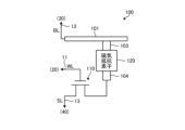
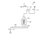
- FIGS. 2 and 3 are diagrams each showing a configuration example of the memory cell 100 according to this embodiment. Each figure is a schematic diagram showing a configuration example of the memory cell 100.
- the selection element 110 and the magnetoresistive element 120 of the memory cell 100 are connected in series, and the selection element 110 has a drain (drain terminal), a source (source terminal), and a gate (gate terminal).
- the contact layer 103 or the contact layer 104 corresponds to a connection layer such as a via.
- the magnetoresistive element 120 of the memory cell 100 is connected to the wiring 101 via the contact layer 103 and to the selection element 110 via the contact layer 104.
- the drain of the selection element 110 is connected to the contact layer 104, and the source thereof is connected to the source line 13 (SL).
- the gate of the selection element 110 is connected to the word line 11 (WL).
- the contact layer 103 is connected to the wiring 101 forming the bit line 12 (BL).
- the magnetoresistive element 120 of the memory cell 100 is connected to the wiring 102 via the contact layer 104 and to the selection element 110 via the contact layer 103.
- the selection element 110 has a drain connected to the bit line 12 (BL) and a source connected to the contact layer 103. Further, the gate of the selection element 110 is connected to the word line 11 (WL). Note that the contact layer 104 is connected to the wiring 102 that constitutes the source line 13 (SL). By applying an on-voltage to the word line 11 (WL), the selection element 110 becomes conductive, and a voltage can be applied to the magnetoresistive element 120.
- the word line 11 (WL) is connected to the word line control circuit 20 (see FIG. 1) as described above.
- the bit line 12 (BL) is connected to a bit line control circuit 30 (see FIG. 1).
- the source line 13 (SL) is connected to the sense amplifier 40 (see FIG. 1).
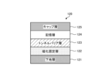
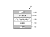
- FIGS. 4 and 5 are diagrams each showing a configuration example of the magnetoresistive element 120 according to this embodiment. Each figure is a cross-sectional view showing a configuration example of the magnetoresistive element 120.
- the magnetoresistive element 120 includes a base layer 121, a magnetization fixed layer 122, a tunnel barrier layer (insulating layer) 123, a storage layer (free layer) 124, and a cap layer 125. Equipped with.
- the magnetoresistive element 120 shown in FIG. 4 is constructed by laminating a base layer 121, a magnetization fixed layer 122, a tunnel barrier layer 123, a storage layer 124, and a cap layer 125 in this order.
- the magnetoresistive element 120 shown in FIG. 5 is configured by laminating a base layer 121, a storage layer 124, a tunnel barrier layer 123, a magnetization fixed layer 122, and a cap layer 125 in this order.
- the base layer 121 is made of noble metal or transition metal elements such as Cr, Ta, Ru, Au, Ag, Cu, Al, Ti, V, Mo, Zr, Hf, Re, W, Pt, Pd, Ir, Rh, etc. Layers and stacked structures thereof can be used. Further, the base layer 121 can also be made of a conductive nitride such as TiN. For example, the base layer 121 is made of a film for controlling the crystal orientation of the magnetization fixed layer 122 and improving the adhesion strength to the lower electrode.
- the magnetization fixed layer 122 is a layer that has magnetic anisotropy and whose magnetization direction remains unchanged.
- This magnetization fixed layer 122 can be made of, for example, CoFeB, CoFeC alloy, NiFeB alloy, NiFeC alloy, or the like.
- the magnetization fixed layer 122 can also have a laminated ferripin structure in which a plurality of ferromagnetic layers are laminated with a nonmagnetic layer interposed therebetween.
- Co, CoFe, CoFeB, etc. can be used as the material of the ferromagnetic layer constituting the magnetization fixed layer 122 of this laminated ferripin structure.
- Ru, Re, Ir, Os, etc. can be used as the material of the nonmagnetic layer.
- the magnetization fixed layer 122 can have a structure in which the direction of magnetization thereof is fixed by utilizing antiferromagnetic coupling between an antiferromagnetic layer and a ferromagnetic layer.
- the material for the antiferromagnetic layer include magnetic materials such as FeMn alloy, PtMn alloy, PtCrMn alloy, NiMn alloy, IrMn alloy, NiO, and Fe2O3.
- non-magnetic elements such as Ag, Cu, Au, Al, Si, Bi, Ta, B, C, O, N, Pd, Pt, Zr, Hf, Ir, W, Mo, Nb, etc. are added to these magnetic materials. can also be added.
- the tunnel barrier layer 123 is arranged adjacent to a storage layer 124, which will be described later, and applies an electric field to the storage layer 124 to impart a voltage-controlled magnetic anisotropy effect.
- This tunnel barrier layer 123 is made of an oxide of at least one element selected from the group of Mg, Al, Ti, Si, Zn, Zr, Hf, Ta, Bi, Cr, Ga, La, Gd, Sr, and Ba.
- it may be composed of a nitride of at least one element selected from the group of Mg, Al, Ti, Si, Zn, Zr, Hf, Ta, Bi, Cr, Ga, La, Gd, Sr, and Ba. can.
- the tunnel barrier layer 123 is preferably 0.6 nm or more.
- the memory layer 124 is a layer that has magnetic anisotropy and has a variable magnetization direction. Furthermore, the storage layer 124 is a layer having a VCMA effect.
- the states in which the magnetization direction of the storage layer 124 is the same as and different from the magnetization direction of the fixed magnetization layer 122 are referred to as a parallel state and an antiparallel state, respectively.
- the magnetoresistive element 120 is in a low resistance state when it is in a parallel state, and is in a high resistance state when it is in an antiparallel state. By applying a voltage to the magnetoresistive element 120 as described above, the magnetization direction of the storage layer 124 can be changed.
- the memory layer 124 can be made of cobalt iron (CoFe), cobalt iron boron (CoFeB), Fe, iron boride (FeB), or the like.
- structures containing transition metals Hf, Ta, W, Re, Ir, Pt, Au, Zr, Nb, Mo, Ru, Rh, Pd, Ag, Ti, V, Cr, Mn, Ni, Cu), etc. You can also pick it up. Further, it may also contain nitrides and oxides.
- iridium (Ir) or osmium (Os) can be used as a material that induces a proximity magnetic moment to a magnetic material. Note that the voltage-controlled magnetic anisotropy effect can also be improved by adding a heavy metal to the memory layer 124.
- the thickness of the memory layer 124 is preferably 3.0 nm or less.
- the memory layer 124 may have a laminated structure in which a plurality of ferromagnetic layers are laminated with a nonmagnetic layer interposed therebetween. At this time, two ferromagnetic layers adjacent to each other via a nonmagnetic layer may be exchange-coupled.
- This non-magnetic layer contains Mg, Al, Ti, Si, Zn, Zr, Hf, Ta, Bi, Cr, Ga, La, Gd, Sr, Ba, W, Re, Ir, Pt, Au, Nb, Mo. , Ru, Rh, Pd, Ag, V, Mn, Ni, Cu, etc.
- the cap layer 125 is a layer that prevents metal from diffusing from the wiring member connected to the magnetoresistive element 120.
- This cap layer 125 can be made of metal such as Cr, Ta, Ru, Au, Ag, Cu, Al, Ti, V, Mo, Zr, Hf, Re, W, Pt, Pd, Ir, Rh, etc. .
- the cap layer 125 can be formed of a layer made of an alloy or a transition metal element containing these elements. Further, the cap layer 125 can also be formed by laminating these layers. Further, the cap layer 125 can also be made of a conductive nitride such as TiN.
- the various layers described above can be formed by, for example, sputtering, ion beam deposition, physical vapor deposition (PVD) such as vacuum evaporation, and chemical vapor deposition (ALD) such as atomic layer deposition. It can be manufactured using a phase epitaxy (CVD) method. Furthermore, patterning of these layers can be performed by reactive ion etching (RIE) or ion milling. Preferably, the various layers are formed successively in a vacuum apparatus, followed by patterning.
- PVD physical vapor deposition
- ALD chemical vapor deposition
- RIE reactive ion etching
- ion milling ion milling
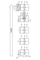
- FIG. 6 is a diagram for explaining the distinguishable resistance states of the magnetoresistive element 120 according to this embodiment.
- the magnetoresistive element 120 has five distinguishable resistance states.
- layers other than the main magnetization fixed layer 122, tunnel barrier layer 123, and storage layer 124 in the magnetoresistive element 120 are appropriately omitted. This also applies to the subsequent FIGS. 7 to 8.
- the five resistance states are "weak short,” “0,” “1,” “complete short,” and “open.”
- the applied voltages for changing these five resistance states are supplied to the magnetoresistive element 120 by the write circuit 60.
- the applied voltage increases from left to right of the arrow in FIG. Note that the relationship between the individual resistance values of "weak short”, “0”, “1”, “complete short”, and “open” will be described in detail later.
- the magnetoresistive element 120 changes from an initial resistance state (for example, a "weak short” resistance state) to a "0" resistance state when a first voltage is applied, and then changes to a "0" resistance state when a second voltage (>first voltage) is applied. When this occurs, the resistance state becomes “1". Furthermore, the magnetoresistive element 120 becomes a "completely shorted” resistance state when a third voltage (>second voltage) is applied, and becomes an "open” resistance state when a fourth voltage (>third voltage) is applied. state.
- an initial resistance state for example, a "weak short” resistance state
- a second voltage >first voltage
- the initial resistance state is, for example, a "weak short” resistance state, but is not limited to this.
- This "weak short” resistance state is a state in which the magnetization fixed layer 122 and the storage layer 124 are electrically connected through the conductive layer 126.
- the conductive layer 126 is, for example, an altered layer.
- the altered layer is, for example, a layer formed by altering one or both of the magnetization fixed layer 122 and the storage layer 124.
- Such a conductive layer 126 is provided on the outer peripheral surface of the magnetoresistive element 120 so as to cross the tunnel barrier layer 123.
- the conductive layer 126 is formed, for example, by narrowing the space of the memory cell 100, by skipping trimming to remove deposits (for example, re-deposition) that will become the conductive layer 126, or by intentionally dropping metal. It is formed by this.
- the conductive layer 126 is formed on the outer peripheral surface of the magnetoresistive element 120, it is not limited thereto, and may be formed within the tunnel barrier layer 123, for example. However, in order to facilitate the formation of the conductive layer 126, it is desirable to form the conductive layer 126 on the outer peripheral surface of the magnetoresistive element 120.
- the magnetoresistive element 120 When the above-mentioned first voltage, second voltage, third voltage, or fourth voltage is applied to the magnetoresistive element 120, a blow current flows through the magnetoresistive element 120, and the conductive layer 126 is destroyed and becomes non-conductive. , the resistance state of the magnetoresistive element 120 changes depending on the first voltage, second voltage, third voltage, or fourth voltage applied to the magnetoresistive element 120.
- the magnetoresistive element 120 changes from its initial resistance state to a "0" resistance state.
- This "0" resistance state is a state in which the magnetization direction of the magnetization fixed layer 122 and the magnetization direction of the storage layer 124 are parallel to each other.
- the magnetoresistive element 120 changes from its initial resistance state to a resistance state of "1".
- This resistance state of "1" is a state in which the magnetization direction of the magnetization fixed layer 122 and the magnetization direction of the storage layer 124 are antiparallel to each other. Note that the magnetoresistive element 120 can return from the resistance state of "1" to the resistance state of "0" by applying the first voltage.
- the magnetoresistive element 120 changes from its initial resistance state to a "completely shorted" resistance state.
- This "completely short-circuit" resistance state is a state in which the tunnel barrier layer 123 is destroyed and is in an energized state.
- the resistance state of the magnetoresistive element 120 can be changed to five resistance states by applying a voltage.
- the magnetoresistive element 120 can change from a "weak short” resistance state to any one of “0", “1”, “complete short”, and “open” resistance state, and can change from “0" to "0". It is possible to change the resistance state from the resistance state to "1”, “completely shorted” or “open”, and from the resistance state "1" to "0", “completely shorted” or “open”. It is possible to go from a "complete short” resistance state to an "open” resistance state.
- the magnetoresistive element 120 is an element in which information can be rewritten.
- the applied voltage supply current
- multi-leveling By determining which of the five resistance states such a magnetoresistive element 120 is in, multi-leveling can be realized. In other words, according to this embodiment, information can be recorded in multiple values, and furthermore, information can be rewritten. In addition, in order to determine which of the five resistance states the resistance state of the magnetoresistive element 120 is, a means for setting a threshold value to realize multi-value will be described in detail below.
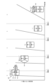
- FIG. 7 is a diagram for explaining multi-leveling based on the distinguishable resistance state of the magnetoresistive element 120 according to this embodiment.
- multi-value bits (5-value bits) of 0, 1, 2, 3, and 4 are realized according to the five distinguishable resistance states of the magnetoresistive element 120.
- 5-value bits a maximum of 5-value bits is realized, the present invention is not limited to this, and for example, 4-value bits of 0, 1, 2, and 3 may be realized.
- FIG. 7 a graph showing the relationship between the resistance value and the amount of variation ( ⁇ ) in the resistance value for each resistance state of the magnetoresistive element 120 is shown.
- the resistance value of the magnetoresistive element 120 increases in the order of "complete short-circuit,” “weak short-circuit,” “0,” “1,” and “open” resistance states. Note that the "weak short” resistance state has a higher resistance value than the "complete short” resistance state.
- information 0 to 4 are associated with the five resistance states of the magnetoresistive element 120. Specifically, a resistance state of "complete short” is associated with 0, a resistance state of "weak short” is associated with 1, a resistance state of "0” is associated with 2, and a resistance state of "1” is associated with resistance state 1. is mapped to 3, and the "open” resistance state is mapped to 4. Then, four threshold values A1, A2, A3, and A4 are set by the readout circuit 50 for the five resistance states. Information is read out by the readout circuit 50 according to these threshold values A1, A2, A3, and A4.
- the information when the resistance value of the magnetoresistive element 120 is below the threshold value A1, the information is 0, and when the resistance value of the magnetoresistive element 120 is below the threshold value A2, which is higher than the threshold value A1, the information is 1, When the resistance value of the magnetoresistive element 120 is less than or equal to the threshold value A3 which is higher than the threshold value A2, the information is 2. If the resistance value of the magnetoresistive element 120 is less than or equal to the threshold value A4, which is higher than the threshold value A3, the information is 3, and if the resistance value of the magnetoresistive element 120 is higher than the threshold value A4, the information is 4.
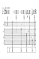
- FIG. 8 is a diagram for explaining quaternization based on the distinguishable resistance state of the magnetoresistive element 120 according to this embodiment.
- the resistance value of the magnetoresistive element 120 is approximately 0-100 ( ⁇ ) in the “complete short” resistance state, approximately 1000 ( ⁇ ) in the “weak short” resistance state, and “ It is about 4000 ( ⁇ ) in the resistance state of “0” and about 12500 ( ⁇ ) in the resistance state of “1”. Accordingly, the threshold Th is set to, for example, 500 ( ⁇ ), 2000 ( ⁇ ), or 8000 ( ⁇ ).
- the readout circuit 50 reads the resistance value of the magnetoresistive element 120 with the threshold value Th set to 500 ( ⁇ ), and takes in the comparison result between the resistance value and the threshold value Th to the first register (1st). For example, the readout circuit 50 compares the read resistance value with 500 ( ⁇ ), and if it determines that the read resistance value is less than 500 ( ⁇ ), the readout circuit 50 sets the determination result to 0 and sets the read resistance value to 500 ( ⁇ ). ( ⁇ ), the determination result is set to 1, and the determination result of 0 or 1 is taken into the first register (1st).
- the readout circuit 50 reads the resistance value of the magnetoresistive element 120 with the threshold value Th set to 2000 ( ⁇ ), and takes in the comparison result between the resistance value and the threshold value Th to the second register (2nd). For example, the readout circuit 50 compares the read resistance value with 2000 ( ⁇ ), and if it determines that the read resistance value is less than 2000 ( ⁇ ), the readout circuit 50 sets the determination result to 0 and the read resistance value is 2000 ( ⁇ ) or less. ( ⁇ ), the determination result is set to 1, and the determination result of 0 or 1 is taken into the second register (2nd).
- the readout circuit 50 reads the resistance value of the magnetoresistive element 120 with the threshold value Th set to 8000 ( ⁇ ), and takes in the comparison result between the resistance value and the threshold value Th to the third register (3rd). For example, the readout circuit 50 compares the read resistance value with 8000 ( ⁇ ), and if it determines that the read resistance value is 8000 ( ⁇ ) or less, it sets the determination result to 0 and the read resistance value is 8000 ( ⁇ ) or less. ( ⁇ ), the determination result is set to 1, and the determination result of 0 or 1 is taken into the third register (3rd).
- the readout circuit 50 realizes 4-value conversion (0, 1, 2, 3) based on each comparison result taken from the first register to the third register, that is, each determination result. For example, if the individual determination results of the first register, second register, and third register are 0, the information becomes 0, and if the determination result of the first register is 1 and the individual determination results of the second register and third register are If the determination result is 0, the information becomes 1. Further, if the individual determination results of the first register and the second register are 1 and the determination result of the third register is 0, the information becomes 2, and the individual determination results of the first register, the second register, and the third register are When the determination result is 1, the information becomes 3.
- FIG. 9 is a diagram for explaining quinarization based on the distinguishable resistance state of the magnetoresistive element 120 according to this embodiment.
- the resistance value of the magnetoresistive element 120 is approximately 0-100 ( ⁇ ) in a "complete short” resistance state, and approximately 1000 ( ⁇ ) in a "weak short” resistance state, as in the example of FIG. ( ⁇ ), approximately 4000 ( ⁇ ) in the “0” resistance state, approximately 12500 ( ⁇ ) in the “1” resistance state, and in addition to the example in Figure 8, the “open” resistance state and ⁇ ( ⁇ ). Therefore, the threshold Th is set to, for example, 500 ( ⁇ ), 2000 ( ⁇ ), 8000 ( ⁇ ), and 20000 ( ⁇ ).
- the readout circuit 50 reads the resistance value of the magnetoresistive element 120 with the threshold Th set at 500 ( ⁇ ), as in the example of FIG. ) is loaded into the first register (1st), the resistance value of the magnetoresistive element 120 is read out with the threshold value Th set to 2000 ( ⁇ ), and the comparison result (discrimination result) between the resistance value and the threshold value Th is stored in the second register (2nd). Incorporate into.
- the readout circuit 50 reads the resistance value of the magnetoresistive element 120 with the threshold value Th set to 8000 ( ⁇ ), loads the comparison result (discrimination result) between the resistance value and the threshold value Th into a third register (3rd), and sets the threshold value Th to the third register (3rd).
- the resistance value of the magnetoresistive element 120 is read with Th set to 20000 ( ⁇ ), and the comparison result (discrimination result) between the resistance value and the threshold value Th is taken into the fourth register (4th).
- the readout circuit 50 realizes quinarization (0, 1, 2, 3, 4) based on each comparison result taken from the first register to the fourth register, that is, each discrimination result. For example, if the individual determination results of the first register, second register, third register, and fourth register are 0, the information becomes 0, and the determination result of the first register is 1, and the second register, third register When the individual determination results of the register and the fourth register are 0, the information becomes 1. Further, if the individual determination results of the first register and the second register are 1, and the determination results of the third register and the fourth register are 0, the information becomes 2, and the information of the first register, the second register, and the third register is 0. When the determination result of each register is 1 and the determination result of the fourth register is 0, the information becomes 3. When the individual determination results of the first register, second register, third register, and fourth register are 1, the information becomes 4.
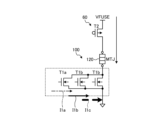
- FIG. 10 is a diagram showing a configuration example of the read circuit 50 and the write circuit 60 according to this embodiment.
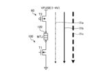
- 11 and 12 are diagrams each illustrating a configuration example of the write circuit 60 according to this embodiment.
- the read circuit 50 includes a charge transistor T3, a bit line selection transistor T4, a reference voltage generator 51, and a comparator 52.
- the parts are arranged in columns.
- This readout circuit 50 is a circuit that reads (discriminates) information recorded in multi-values in the magnetoresistive element 120 from the memory cell 100 to be read.
- the reference voltage generator 51 corresponds to a generation section
- the comparator 52 corresponds to a determination section.
- the charge transistor T3 is a transistor that is turned on in response to a control signal FC(a) applied to its gate terminal.
- the charge transistor T3 is composed of a PMOS type FET (Field Effect Transistor).
- the source terminal of the charge transistor T3 is connected to the potential line of the power supply voltage VDD, the drain terminal is connected to the input terminal of the comparator 52, and the gate terminal is connected to the output terminal of the word line control circuit 20 (or control circuit 5).
- the bit line selection transistor T4 is turned on when a low level control signal FA(n) is input to its gate terminal, and turned off when a high level control signal FA(n) is inputted to its gate terminal.
- the bit line selection transistor T4 is a transistor that is turned on in response to a control signal CL applied to its gate terminal. This bit line selection transistor T4 is connected to the magnetoresistive element 120.
- the bit line selection transistor T4 is composed of an NMOS type FET.
- the source terminal of the bit line selection transistor T4 is connected to one end of the magnetoresistive element 120, the drain terminal is connected to the input terminal of the comparator 52, and the gate terminal is connected to the output terminal of the word line control circuit 20 (or control circuit 5). It is connected.
- the bit line selection transistor T4 is turned on when a high level control signal FA(n) is input to its gate terminal, and turned off when a low level control signal FA(n) is inputted to its gate terminal.
- the reference voltage generator 51 includes a plurality of reference transistors T5 to T9 and a plurality of reference resistance elements R1 to R3. This reference voltage generator 51 is a circuit that generates a reference voltage (reference voltage signal) that becomes a reference (threshold value) when reading out multi-level information recorded in the magnetoresistive element 120.
- the first reference transistor T5 is a transistor that is turned on in response to a control signal RC applied to its gate terminal.
- the first reference transistor T5 is composed of a PMOS type FET.
- the source terminal of the first reference transistor T5 is connected to the potential line of the power supply voltage VDD, the drain terminal is connected to the input terminal of the comparator 52, and the gate terminal is connected to the output terminal of the control circuit 5.
- the first reference transistor T5 is turned on when the low level control signal RC is input to its gate terminal, and turned off when the high level control signal RC is inputted to the first reference transistor T5.
- the second reference transistor T6 is a transistor that is turned on in response to a control signal RCL applied to its gate terminal.
- the second reference transistor T6 is composed of an NMOS type FET.
- the source terminal of the second reference transistor T6 is connected to one end of each of the reference resistance elements R1 to R3, the drain terminal is connected to the input terminal of the comparator 52, and the gate terminal is connected to the output terminal of the control circuit 5.
- the second reference transistor T6 is turned on when the high-level control signal RCL is input to its gate terminal, and turned off when the low-level control signal RCL is input to the second reference transistor T6.
- the third to fifth reference transistors T7 to T9 are transistors that are turned on in response to control signals RA (RA1, RA2, RA3) applied to their respective gate terminals.
- the third to fifth reference transistors T7 to T9 are each configured with an NMOS type FET.
- the individual source terminals of the third to fifth reference transistors T7 to T9 are connected to the ground potential (GND), the individual drain terminals are respectively connected to one end of each of the reference resistance elements R1 to R3, and the individual gate terminals of the third to fifth reference transistors T7 to T9 are connected to the ground potential (GND). are connected to each output terminal of the control circuit 5, respectively.
- the third to fifth reference transistors T7 to T9 are turned on when a high level control signal RA (RA1, RA2, RA3) is input to their gate terminals, and turned off when a low level control signal RA is inputted to their gate terminals. state.
- RA high level control signal
- Each of the reference resistance elements R1 to R3 is a resistance element that defines a resistance value.
- the reference resistance element R1 is a resistance element having a resistance of 500 ( ⁇ ).
- the reference resistance element R2 is a resistance element having a resistance of 2000 ( ⁇ ).
- the reference resistance element R3 is a resistance element having a resistance of 8000 ( ⁇ ).
- One end of each of the reference resistance elements R1 to R3 is connected to the source terminal of the second reference transistor T6, and the other end of each of the reference resistance elements R1 to R3 is connected to the drain terminal of each of the third to fifth reference transistors T7 to T9, respectively. It is connected.
- the reference voltage generator 51 having such a configuration generates a reference voltage Vref according to the individual resistance values of each of the reference resistance elements R1 to R3, for example, 500 ( ⁇ ), 2000 ( ⁇ ), and 8000 ( ⁇ ). This reference voltage Vref functions as a threshold value.
- the reference voltage generator 51 supplies a low level control signal RC, a high level control signal RCL, and a high level control signal to each gate of the first to third reference transistors T5 to T7 in order to generate the first reference current I3.
- a signal RA1 is supplied to each.
- the first to third reference transistors T5 to T7 are turned on, the reference resistance element R1 is biased, and the first reference current I3 is generated.
- the first reference current I3 flows from the power supply voltage VDD toward the ground potential via the reference resistance element R1.
- the reference voltage generator 51 sends a low-level control signal RC and a high-level control signal to each gate of the first, second, and fourth reference transistors T5, T6, and T8.
- a signal RCL and a high level control signal RA2 are respectively supplied.
- the first, second, and fourth reference transistors T5, T6, and T8 are turned on, the reference resistance element R2 is biased, and the second reference current I4 is generated.
- the second reference current I4 flows from the power supply voltage VDD toward the ground potential via the reference resistance element R2.
- the reference voltage generator 51 sends a low-level control signal RC and a high-level control signal to each gate of the first, second, and fifth reference transistors T5, T6, and T9.
- a signal RCL and a high level control signal RA3 are respectively supplied.
- the first, second, and fifth reference transistors T5, T6, and T9 are turned on, the reference resistance element R3 is biased, and the third reference current I5 is generated.
- the third reference current I5 flows from the power supply voltage VDD toward the ground potential via the reference resistance element R3.
- the comparator 52 is composed of, for example, a sense amplifier.
- the comparator 52 corresponds to the sense amplifier 40 (see FIG. 1), and the readout circuit 50 includes the sense amplifier 40; however, the readout circuit 50 and the sense amplifier 40 are not limited to this. It is also possible to provide it as a separate body. In this case, the readout circuit 50 and sense amplifier 40 correspond to the readout section.
- the comparator 52 has a pair of input terminals.
- One input terminal of the comparator 52 is connected to a connection point P1 (hereinafter referred to as the first connection point P1) between the drain terminal of the charge transistor T3 and the drain terminal of the bit line selection transistor T4 in the readout circuit 50.
- the other input terminal of the comparator 52 is connected to a connection point P2 (hereinafter referred to as a second connection point P2) between the drain terminal of the first reference transistor T5 and the drain terminal of the second reference transistor T6 in the reference voltage generator 51. )It is connected to the.
- This comparator 52 has a voltage Vm (voltage related to the resistance value of the magnetoresistive element 120) at the first connection point P1 inputted to one input terminal, and a reference voltage Vm at the second connection point P2 inputted to the other input terminal. It compares the voltage (threshold voltage) with Vref and outputs the comparison result.
- Vm voltage related to the resistance value of the magnetoresistive element 120
- write circuit 60 includes a fuse transistor T2.
- the memory cell 100 includes a selection transistor T1 and a magnetoresistive element 120.
- the selection transistor T1 is an example of the selection element 110 and can function as part of the write circuit 60.
- the selection transistor T1 is a transistor that is turned on in response to a control signal FA(n) applied to its gate terminal. This selection transistor T1 is connected to the magnetoresistive element 120.
- the selection transistor T1 is composed of an NMOS type FET. The source terminal of this selection transistor T1 is connected to the ground potential (GND), the drain terminal is connected to one end of the magnetoresistive element 120, and the gate terminal is connected to the output terminal of the word line control circuit 20 (or control circuit 5). ing. Note that the selection transistor T1 is turned on when a high level control signal FA(n) is input to its gate terminal, and turned off when a low level control signal FA(n) is inputted thereto.
- the fuse transistor T2 is a transistor that is turned on in response to a control signal FB(a) applied to its gate terminal.
- This fuse transistor T2 is connected to the magnetoresistive element 120.
- the fuse transistor T2 is composed of a PMOS type FET.
- the source terminal of this fuse transistor T2 is connected to the power supply voltage VFUSE, the drain terminal is connected to one end of the magnetoresistive element 120, and the gate terminal is connected to the output terminal of the bit line control circuit 30 (or control circuit 5). .
- the fuse transistor T2 is turned on when the low level control signal FB(a) is input to its gate terminal, and turned off when the high level control signal FB(a) is inputted to its gate terminal.
- the power supply voltage VFUSE can be changed within the range of 1 to 4V.
- This power supply voltage VFUSE is changed by the control circuit 5 according to the information to be written (for example, 0, 1, 2, 3), and supplies the magnetoresistive element 120 with a plurality of currents I1a, I1b, and I1c having different magnitudes.
- the power supply voltage VFUSE is a first voltage that changes the magnetoresistive element 120 from a certain resistance state (for example, a "weak short" resistance state) to a state of "0";
- a second voltage (>first voltage) that brings the magnetoresistive element 120 into a "completely shorted" state from a certain resistance state is generated (>second voltage).
- the power supply voltage VFUSE may be generated by the voltage generation circuit 6.
- a plurality of voltages (currents) of different magnitudes can be applied to the magnetoresistive element 120 by means other than changing the voltage value of the power supply voltage VFUSE and supplying a plurality of voltages (currents) of different magnitudes to the magnetoresistive element 120. It is possible to supply For example, the power supply voltage VFUSE may be kept constant, and the power supply voltage VFUSE may be raised and lowered by a raising/lowering circuit to supply a plurality of voltages having different magnitudes to the magnetoresistive element 120.
- three selection transistors T1a, T1b, and T1c may be provided in parallel (in the case of quaternary conversion). These selection transistors T1a, T1b, and T1c function as part of the write circuit 60. In order to generate voltages (currents) of different magnitudes, the write circuit 60 performs a first operation in which only the selection transistor T1a is turned on, a second operation in which only the two selection transistors T1a and T1b are turned on, and A third operation is performed to turn on the three selection transistors T1a, T1b, and T1c.
- the voltage (current) supplied to the magnetoresistive element 120 changes depending on the number of selection transistors T1a, T1b, and T1c in the on state. As a result, a plurality of currents I1a, I1b, and I1c having different magnitudes are supplied to the magnetoresistive element 120. Note that in the case of quinarization, four selection transistors are provided in parallel.
- all transistors T1 to T9 shown in FIG. 10 are in an off state.
- the selection transistor T1 and the fuse transistor T2 are turned on.
- a high level control signal FA(n) is supplied to the selection transistor T1
- a low level control signal FB(a) is supplied to the fuse transistor T2.
- a current I1 flows from the potential line of VFUSE to the magnetoresistive element 120 via the fuse transistor T2.
- VFUSE (1 to 4 V) is changed by the control circuit 5 depending on the information to be written (for example, 0, 1, 2, 3).
- a first voltage, a second voltage, and a third voltage are generated as described above.
- a first current I1a, a second current I1b, and a third current I1c are generated (see FIG. 11).
- the magnetoresistive element 120 changes from a certain resistance state (eg, "weak short") to a "0" resistance state.
- the magnetoresistive element 120 changes from a certain resistance state to a resistance state of "1".
- the third current I1c flows through the magnetoresistive element 120, the magnetoresistive element 120 changes from a certain resistance state to a "completely shorted” resistance state. As a result, data (0, 1, 2, 3) is written to the magnetoresistive element 120.
- the selection transistor T1, charge transistor T3, and bit line selection transistor T4 are turned on. At this time, a high control signal FA(n) is supplied to the selection transistor T1, a low level control signal FC(a) is supplied to the charge transistor T3, and a high control signal CL is supplied to the bit line selection transistor T4. Ru.
- the magnetoresistive element 120 as the read target is selected, and the read current I2 flows from the charge transistor T3 to the magnetoresistive element 120 via the bit line selection transistor T4.
- the path through which this read current I2 flows is the bias path of the magnetoresistive element 120.
- the voltage Vm at the first connection point P1 is input to the first input terminal of the comparator 52 in accordance with the read current I2.
- the third to fifth reference transistors T5 to T7 of the reference voltage generator 51 are turned on.
- the reference voltage generator 51 supplies a low level control signal RC, a high level control signal RCL, and a high level control signal RA1 to each gate of the third to fifth reference transistors T5 to T7, respectively.
- the first reference resistance element R1 is biased by the power supply voltage VDD in the reference voltage generator 51, and the first reference current I3 is generated.
- the reference voltage Vref of the second connection point P2 is input to the second input terminal of the comparator 52 according to the first reference current I3.
- the comparator 52 compares the voltage (Vm) at the first connection point P1 in the readout circuit 50 with the second connection in the reference voltage generator 51 with the first reference current I3 flowing through the first reference resistance element R1.
- the state of the magnetoresistive element 120 is read by comparing it with the reference voltage (Vref) at point P2 (first comparison operation).
- the first comparison operation when the read current I2 flows through the magnetoresistive element 120, the potential (Vm) of the first connection point P1 becomes a potential corresponding to the resistance value of the magnetoresistive element 120.
- the potential (Vref) at the second connection point P2 when a current flows through the first reference resistance element R1, the potential (Vref) at the second connection point P2 is equal to the resistance value (for example, 500 ( ⁇ )) of the first reference resistance element R1. ). Therefore, the first comparison operation between the voltage signal SA1 (Vm) and the reference voltage signal SA2 (Vref) in the comparator 52 essentially involves the resistance value of the magnetoresistive element 120 and the resistance value of the first reference resistance element R1 (i.e. This is equivalent to the operation of comparing the first threshold value).
- the comparator 52 determines whether the voltage Vm at the first connection point P1 is less than or equal to the reference voltage Vref at the second connection point P2 (Vm ⁇ Vref). When the comparator 52 determines that the voltage Vm is less than or equal to the reference voltage Vref, the comparator 52 outputs a signal (comparison result) corresponding to information "0". On the other hand, if it is determined that the voltage Vm is greater than the reference voltage Vref, a signal (comparison result) corresponding to the information "1" is output. This information is stored by the first register of the readout circuit 50. After that, the read circuit 50 performs a second comparison operation.
- the comparator 52 compares the voltage (Vm) at the first connection point P1 in the readout circuit 50 with the second connection in the reference voltage generator 51 with the second reference current I4 flowing through the second reference resistance element R2.
- the state of the magnetoresistive element 120 is read by comparing it with the reference voltage (Vref) at point P2 (second comparison operation).
- This second comparison operation is similar to the first comparison operation except that the reference voltage Vref serving as a threshold value is different from the first comparison operation.
- the reference voltage Vref has a potential corresponding to the resistance value (for example, 2000 ( ⁇ )) of the second reference resistance element R2.
- the information “0” or “1” is stored by the second register of the readout circuit 50.
- the read circuit 50 performs a third comparison operation.
- the comparator 52 compares the voltage (Vm) at the first connection point P1 in the readout circuit 50 with the second connection in the reference voltage generator 51 with the third reference current I5 flowing through the third reference resistance element R3.
- the state of the magnetoresistive element 120 is read by comparing it with the reference voltage (Vref) at point P2 (third comparison operation).
- This second comparison operation is similar to the first comparison operation except that the reference voltage Vref serving as a threshold value is different from the first comparison operation.
- the reference voltage Vref has a potential corresponding to the resistance value (for example, 8000 ( ⁇ )) of the third reference resistance element R3.
- information “0” or “1” is stored by the third register of the readout circuit 50. Thereafter, the read circuit 50 ends the comparison operation.
- the readout circuit 50 realizes 4-value conversion (0, 1, 2, 3) based on each comparison result taken from the first register to the fourth register, that is, the determination result (see FIG. 8). For example, if the individual determination results of the first register, second register, and third register are 0, the information becomes 0, and if the determination result of the first register is 1 and the individual determination results of the second register and third register are If the determination result is 0, the information becomes 1. Further, if the individual determination results of the first register and the second register are 1 and the determination result of the third register is 0, the information becomes 2, and the individual determination results of the first register, the second register, and the third register are When the determination result is 1, the information becomes 3.
- the method for reading information from the magnetoresistive element 120 is not limited to the above-mentioned example. Any method can be used to read information from the magnetoresistive element 120 as long as it can identify the resistance state of the magnetoresistive element 120 using three threshold values. For example, in the above description, the first comparison operation is performed first, then the second comparison operation is performed, and finally, the third comparison operation is performed, but the order of these comparison operations may be reversed.
- the comparison operation is performed three times, but it is also possible to switch whether or not to perform the next comparison operation depending on the comparison result.
- the process proceeds to the second comparison operation, and only when it is determined that the voltage Vm is greater than the reference voltage Vref in the second comparison operation, the third comparison is performed. You may proceed to the operation.
- the comparator 52 determines that the voltage Vm is equal to or lower than the reference voltage Vref in the first comparison operation, it outputs a signal (comparison result) corresponding to the information "0", and in the second comparison operation, the comparator 52 outputs a signal (comparison result) corresponding to the information "0".
- a signal (comparison result) corresponding to the information "1" is output.
- the comparator 52 determines that the voltage Vm is equal to or lower than the reference voltage Vref in the third comparison operation, it outputs a signal (comparison result) corresponding to the information "2", and in the third comparison operation, the voltage Vm is lower than or equal to the reference voltage Vref. If it is determined that the voltage is higher than the reference voltage Vref, a signal (comparison result) corresponding to information "3" is output.
- the comparison operation is performed three times to realize 4-value conversion, but when realizing 5-value conversion, a necessary circuit including a fourth reference resistance element etc. is added, It is sufficient to perform the same comparison operation as described above four times.
- the storage device 1 includes a magnetoresistive element (magnetoresistive storage element) 120 that changes into at least four distinguishable resistance states, and a magnetoresistive element that changes the magnetization direction of the magnetoresistive element 120. and a writing section (for example, a writing circuit 60) that changes the magnetoresistive element 120 into at least four distinguishable resistance states by causing the magnetoresistive element 120 to change or to apply a blow current to the magnetoresistive element 120.
- a magnetoresistive element 120 that changes into at least four distinguishable resistance states
- a writing circuit 60 that changes the magnetoresistive element 120 into at least four distinguishable resistance states by causing the magnetoresistive element 120 to change or to apply a blow current to the magnetoresistive element 120.
- the magnetoresistive element 120 also includes a magnetization fixed layer 122, a storage layer 124, an insulating layer (for example, a tunnel barrier layer 123) provided between the magnetization fixed layer 122 and the storage layer 124, and a magnetization fixed layer 122 and a storage layer 124.
- a conductive layer 126 connecting the memory layer 124 may also be included. This ensures that the magnetoresistive element 120 can be changed into at least four distinguishable resistance states.
- the writing section may also apply a blow current to the magnetoresistive element 120 to destroy the conductive layer 126 and make it non-conductive. Thereby, the resistance state of the magnetoresistive element 120 can be changed.
- the writing section may also apply a blow current to the magnetoresistive element 120 to break the insulating layer and make it conductive. Thereby, the resistance state of the magnetoresistive element 120 can be changed.
- the magnetoresistive element 120 further includes a connection layer (for example, the contact layer 103 or the contact layer 104) laminated on the magnetization fixed layer 122 or the storage layer 124, and the writing section applies a blow current to the magnetoresistive element 120.
- the connection layer may be destroyed and rendered non-conductive. Thereby, the resistance state of the magnetoresistive element 120 can be changed.
- the four resistance states may include a resistance state in which the conductive layer 126 is broken and is in a non-conductive state. This makes it possible to achieve at least four distinguishable resistance states.
- the four resistance states may include a resistance state in which the insulating layer is broken and is in a conductive state. This makes it possible to achieve at least four distinguishable resistance states.
- the magnetoresistive element 120 further includes a connection layer (for example, a contact layer 103 or a contact layer 104) stacked on the magnetization fixed layer 122 or the storage layer 124, and the four resistance states are determined by the connection layer being destroyed. It may also include a resistive state that is a non-conducting state. This makes it possible to achieve at least four distinguishable resistance states.
- a connection layer for example, a contact layer 103 or a contact layer 104
- the magnetoresistive element 120 further includes a connection layer (for example, a contact layer 103 or a contact layer 104) stacked on the magnetization fixed layer 122 or the storage layer 124, and the four resistance states are determined by the connection layer being destroyed. It may also include a resistive state that is a non-conducting state. This makes it possible to achieve at least four distinguishable resistance states.
- the four resistance states are a resistance state in which the magnetization direction of the magnetization fixed layer 122 and the magnetization direction of the storage layer 124 are parallel, and a resistance state in which the magnetization direction of the magnetization fixed layer 122 and the magnetization direction of the storage layer 124 are antiparallel. It may also include the state. This makes it possible to achieve at least four distinguishable resistance states.
- the conductive layer 126 may be formed on the outer peripheral surface of the magnetoresistive element 120 so as to cross the insulating layer. Thereby, the conductive layer 126 can be easily formed on the magnetoresistive element 120.
- the conductive layer 126 may be a degraded layer of one or both of the magnetization fixed layer 122 and the storage layer 124. Thereby, the conductive layer 126 can be easily created in the magnetoresistive element 120 using the altered layer.
- the writing unit may change the magnitude of the blow current to change the magnetoresistive element 120 into at least two distinguishable resistance states. Thereby, the resistance state of the magnetoresistive element 120 can be changed reliably.
- the magnetoresistive element 120 is an element that changes into five distinguishable resistance states, and the writing section can change the magnetization direction of the magnetoresistive element 120 or cause a blow current to flow through the magnetoresistive element 120.
- the magnetoresistive element 120 may be changed into five distinguishable resistance states. This realizes quinarization, so the memory capacity can be increased without increasing the number of memory cells 100.
- the writing unit may change the magnitude of the blow current to change the magnetoresistive element 120 into three distinguishable resistance states. Thereby, the resistance state of the magnetoresistive element 120 can be changed reliably.
- the writing section may change the magnitude of the blow current by using a plurality of power supply voltages with different output voltages (for example, power supply voltage VFUSE (1 to 4 V)). Thereby, blow currents having different magnitudes can be easily generated.
- a plurality of power supply voltages with different output voltages for example, power supply voltage VFUSE (1 to 4 V)
- the writing section includes a plurality of transistors (for example, each selection transistor T1a, T1b, T1c) connected in parallel, and changes the conduction and non-conduction of each of the plurality of transistors to change the magnitude of the blow current. You can. Thereby, blow currents having different magnitudes can be easily generated.
- the storage device 1 further includes a readout section (for example, a readout circuit 50) that reads out a voltage related to the resistance value of the magnetoresistive element 120, and the readout section has a plurality of readout sections for determining at least four distinguishable resistance states.
- a generation unit e.g., reference voltage generator 51
- a determination unit e.g., comparator 52
- the voltage and a plurality of reference voltages may have. Thereby, at least four distinguishable resistance states of the magnetoresistive element 120 can be reliably determined.
- the magnetoresistive element 120 is an element that changes into five distinguishable resistance states
- the generation section generates a plurality of reference voltages for discriminating between the five discriminable resistance states
- the discriminating section The voltage and multiple reference voltages may be compared to determine five distinct resistance states. Thereby, the five distinguishable resistance states of the magnetoresistive element 120 can be reliably determined.
- each component of each device shown in the drawings is functionally conceptual, and does not necessarily need to be physically configured as shown in the drawings.
- the specific form of distributing and integrating each device is not limited to what is shown in the diagram, and all or part of the devices can be functionally or physically distributed or integrated in arbitrary units depending on various loads and usage conditions. Can be integrated and configured.
- the imaging device 300, the distance measuring device 400, and the game device 900 use the storage device 1 according to each of the above-described embodiments as a memory.
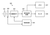
- FIG. 13 is a diagram showing an example of a schematic configuration of the imaging device 300.
- This imaging device 300 is an example of an electronic device to which the storage device 1 according to the present embodiment is applied.
- Examples of the imaging device 300 include electronic devices such as digital still cameras, video cameras, and smartphones and mobile phones that have an imaging function.
- the imaging device 300 includes an optical system 301, a shutter device 302, an image sensor 303, a control circuit (drive circuit) 304, a signal processing circuit 305, a monitor 306, and a memory 307.
- This imaging device 300 is capable of capturing still images and moving images.
- the optical system 301 has one or more lenses. This optical system 301 guides light (incident light) from a subject to an image sensor 303 and forms an image on the light receiving surface of the image sensor 303 .
- the shutter device 302 is arranged between the optical system 301 and the image sensor 303.
- the shutter device 302 controls the light irradiation period and the light blocking period to the image sensor 303 under the control of the control circuit 304.
- the image sensor 303 accumulates signal charges for a certain period of time according to the light that is imaged on the light receiving surface via the optical system 301 and the shutter device 302.
- the signal charge accumulated in the image sensor 303 is transferred according to a drive signal (timing signal) supplied from the control circuit 304.
- the control circuit 304 outputs a drive signal that controls the transfer operation of the image sensor 303 and the shutter operation of the shutter device 302, and drives the image sensor 303 and the shutter device 302.
- the signal processing circuit 305 performs various signal processing on the signal charges output from the image sensor 303.
- An image (image data) obtained by signal processing by the signal processing circuit 305 is supplied to a monitor 306 and also to a memory 307.
- the monitor 306 displays a moving image or a still image captured by the image sensor 303 based on the image data supplied from the signal processing circuit 305.
- a panel display device such as a liquid crystal panel or an organic EL (Electro Luminescence) panel is used.
- the memory 307 stores image data supplied from the signal processing circuit 305, that is, image data of a moving image or a still image captured by the image sensor 303.
- the memory 307 corresponds to the storage device 1 according to the embodiment described above.
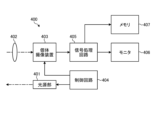
- FIG. 14 is a diagram showing an example of a schematic configuration of the distance measuring device 400.
- This distance measuring device 400 is an example of an electronic device to which the storage device 1 according to the present embodiment is applied.
- the distance measuring device 400 includes a light source section 401, an optical system 402, a solid-state imaging device (image sensor) 403, a control circuit (drive circuit) 404, a signal processing circuit 405, A monitor 406 and a memory 407 are provided.
- This distance measuring device 400 projects light toward a subject from a light source unit 401 and receives light (modulated light or pulsed light) reflected from the surface of the subject, thereby creating a distance image according to the distance to the subject. can be obtained.
- the light source unit 401 emits light toward the subject.
- a vertical cavity surface emitting laser (VCSEL) array that emits laser light as a surface light source or a laser diode array in which laser diodes are arranged in a line is used.
- the laser diode array is supported by a predetermined driving section (not shown) and is scanned in a direction perpendicular to the direction in which the laser diodes are arranged.
- the optical system 402 has one or more lenses. This optical system 402 guides light (incident light) from a subject to a solid-state imaging device 403 and forms an image on a light-receiving surface (sensor section) of the solid-state imaging device 403 .
- the solid-state imaging device 403 accumulates signal charges according to the light that is imaged on the light-receiving surface via the optical system 402. A distance signal indicating the distance determined from the light reception signal (APD OUT) output from the solid-state imaging device 403 is supplied to the signal processing circuit 405.
- a solid-state imaging device such as an image sensor is used.
- the control circuit 404 outputs a drive signal (control signal) that controls the operation of the light source section 401, the solid-state imaging device 403, etc., and drives the light source section 401, the solid-state imaging device 403, etc.
- the signal processing circuit 405 performs various signal processing on the distance signal supplied from the solid-state imaging device 403. For example, the signal processing circuit 405 performs image processing (for example, histogram processing, peak detection processing, etc.) to construct a distance image based on the distance signal. An image (image data) obtained by signal processing by the signal processing circuit 405 is supplied to a monitor 406 and also to a memory 407.
- image processing for example, histogram processing, peak detection processing, etc.
- the monitor 406 displays the distance image captured by the image sensor 303 based on the image data supplied from the signal processing circuit 405.
- a panel display device such as a liquid crystal panel or an organic EL panel is used.
- the memory 407 stores image data supplied from the signal processing circuit 405, that is, image data of a distance image captured by the image sensor 303.
- the memory 407 corresponds to the storage device 1 according to the embodiment described above.
- FIG. 15 is a perspective view (external perspective view) showing an example of a schematic configuration of the game device 900.
- FIG. 16 is a block diagram showing an example of a schematic configuration of game device 900.
- This game device 900 is an example of an electronic device to which the storage device 1 according to the present embodiment is applied.
- the game device 900 has an external appearance in which each component is arranged inside and outside of an outer casing 901 formed in a horizontally long and flat shape, for example.
- a display panel 902 is provided on the front surface of the outer casing 901 at the center in the longitudinal direction. Further, an operation key 903 and an operation key 904 are provided on the left and right sides of the display panel 902, respectively, and are spaced apart from each other in the circumferential direction. Furthermore, an operation key 905 is provided at the lower end of the front surface of the outer casing 901.
- the operation keys 903, 904, and 905 function as direction keys or enter keys, and are used to select menu items displayed on the display panel 902, advance the game, and the like.
- a connection terminal 906 for connecting an external device, a supply terminal 907 for power supply, a light receiving window 908 for infrared communication with the external device, and the like are provided on the top surface of the outer casing 901.
- the game device 900 includes an arithmetic processing unit 910 including a CPU (Central Processing Unit), a storage unit 920 that stores various information, and a control unit 930 that controls each component of the game device 900. Be prepared.
- the arithmetic processing unit 910 and the control unit 930 are supplied with power from, for example, a battery (not shown) or the like.
- the arithmetic processing unit 910 generates a menu screen for allowing the user to set various information or select an application. Further, the arithmetic processing unit 910 executes an application selected by the user.
- the storage unit 920 holds various information set by the user.
- the storage unit 920 corresponds to the storage device 1 according to the embodiment described above.
- the control unit 930 includes an input reception unit 931, a communication processing unit 933, and a power control unit 935.
- the input reception unit 931 detects the states of the operation keys 903, 904, and 905, for example.
- the communication processing unit 933 performs communication processing with external devices.
- Power control section 935 controls power supplied to each section of game device 900.
- the storage device 1 may be mounted on the same semiconductor chip together with a semiconductor circuit forming an arithmetic unit or the like to form a semiconductor device (System-on-a-Chip: SoC).
- SoC System-on-a-Chip
- the storage device 1 can be installed in various electronic devices that can be equipped with a memory (storage unit) as described above.
- the storage device 1 includes an HDD (hard disk drive), a notebook PC (personal computer), a mobile device (for example, a smartphone or a tablet PC), and a PDA (personal digital assistant). , wearable devices, music equipment, and various other electronic devices.
- the storage device 1 is used as various types of memory such as storage.
- the present technology can also have the following configuration.
- a storage device comprising: (2) The magnetoresistive storage element includes a magnetization fixed layer, a storage layer, an insulating layer provided between the magnetization fixed layer and the storage layer, and a conductive layer connecting the magnetization fixed layer and the storage layer. , The storage device according to (1) above.
- the writing unit causes the blow current to flow through the magnetoresistive storage element to destroy the conductive layer and bring it into a non-conductive state.
- the writing unit causes the blow current to flow through the magnetoresistive storage element to destroy the insulating layer and bring it into a conductive state.
- the magnetoresistive storage element further includes a connection layer laminated on the magnetization fixed layer or the storage layer, The writing unit causes the blow current to flow through the magnetoresistive storage element to destroy the connection layer and bring it into a non-conductive state.
- the four resistance states include a resistance state in which the conductive layer is broken and is in a non-conductive state.
- the four resistance states include a resistance state in which the insulating layer is broken and is in a conductive state.
- the magnetoresistive storage element further includes a connection layer laminated on the magnetization fixed layer or the storage layer,
- the four resistance states include a resistance state in which the connection layer is destroyed and is in a non-conducting state.
- the four resistance states include a resistance state in which the magnetization direction of the magnetization fixed layer and the magnetization direction of the storage layer are parallel, and a resistance state in which the magnetization direction of the magnetization fixed layer and the magnetization direction of the storage layer are antiparallel.
- the storage device according to any one of (6) to (8) above. (10) The conductive layer is formed on the outer peripheral surface of the magnetoresistive memory element so as to cross the insulating layer. The storage device according to any one of (2) to (9) above. (11) The conductive layer is a modified layer of one or both of the magnetization fixed layer and the storage layer, The storage device according to any one of (2) to (10) above.
- the writing unit changes the magnitude of the blow current to change the magnetoresistive storage element into at least two distinguishable resistance states.
- the storage device according to any one of (1) to (11) above.
- the magnetoresistive storage element is an element that changes into five distinguishable resistance states
- the writing unit changes the magnetoresistive storage element into the five distinguishable resistance states by changing the magnetization direction of the magnetoresistive storage element or flowing a blow current through the magnetoresistive storage element.
- the writing unit changes the magnitude of the blow current to change the magnetoresistive storage element into the three distinguishable resistance states;
- the storage device according to (13) above.
- the writing unit changes the magnitude of the blow current using a plurality of power supply voltages having different output voltages.
- the storage device has a plurality of transistors connected in parallel, and changes conduction and non-conduction of each of the plurality of transistors to change the magnitude of the blow current.
- the storage device according to any one of (1) to (14) above.
- (17) further comprising a readout unit that reads out a voltage related to the resistance value of the magnetoresistive memory element,
- the reading section includes: a generation unit that generates a plurality of reference voltages for determining the at least four distinguishable resistance states; a determining unit that compares the voltage and the plurality of reference voltages to determine the at least four distinguishable resistance states; has,
- the storage device according to any one of (1) to (16) above.
- the magnetoresistive storage element is an element that changes into five distinguishable resistance states
- the generation unit generates a plurality of reference voltages for determining the five distinguishable resistance states
- the determining unit compares the voltage and the plurality of reference voltages to determine the five distinguishable resistance states.
- the storage device is a magnetoresistive storage element that changes into at least four distinguishable resistance states; a writing unit that changes the magnetoresistive storage element into the at least four distinguishable resistance states by changing the magnetization direction of the magnetoresistive storage element or applying a blow current to the magnetoresistive storage element; Electronic equipment with.
- the resistance state of the magnetoresistive storage element can be identified by changing the magnetization direction of the magnetoresistive storage element, which can be varied into at least four distinguishable resistance states, or by passing a blow current through the magnetoresistive storage element. change into at least four resistance states, How to control storage devices.
- An electronic device comprising the storage device according to any one of (1) to (18) above.
- (22) A method for controlling a storage device, which controls the storage device according to any one of (1) to (18) above.
Landscapes
- Engineering & Computer Science (AREA)
- Computer Hardware Design (AREA)
- Manufacturing & Machinery (AREA)
- Hall/Mr Elements (AREA)
- Mram Or Spin Memory Techniques (AREA)
- Magnetic Heads (AREA)
- Semiconductor Memories (AREA)
Abstract
Priority Applications (1)
| Application Number | Priority Date | Filing Date | Title |
|---|---|---|---|
| US18/881,745 US20260004836A1 (en) | 2022-07-28 | 2023-07-11 | Storage device, electronic apparatus, and storage device control method |
Applications Claiming Priority (2)
| Application Number | Priority Date | Filing Date | Title |
|---|---|---|---|
| JP2022120138A JP2024017480A (ja) | 2022-07-28 | 2022-07-28 | 記憶装置、電子機器及び記憶装置の制御方法 |
| JP2022-120138 | 2022-07-28 |
Publications (1)
| Publication Number | Publication Date |
|---|---|
| WO2024024497A1 true WO2024024497A1 (fr) | 2024-02-01 |
Family
ID=89706202
Family Applications (1)
| Application Number | Title | Priority Date | Filing Date |
|---|---|---|---|
| PCT/JP2023/025590 Ceased WO2024024497A1 (fr) | 2022-07-28 | 2023-07-11 | Dispositif de stockage, appareil électronique, et procédé de commande de dispositif de stockage |
Country Status (3)
| Country | Link |
|---|---|
| US (1) | US20260004836A1 (fr) |
| JP (1) | JP2024017480A (fr) |
| WO (1) | WO2024024497A1 (fr) |
Citations (4)
| Publication number | Priority date | Publication date | Assignee | Title |
|---|---|---|---|---|
| JP2002246567A (ja) * | 2001-02-14 | 2002-08-30 | Toshiba Corp | 磁気ランダムアクセスメモリ |
| JP2008187183A (ja) * | 2007-01-30 | 2008-08-14 | Samsung Electronics Co Ltd | 磁気及び抵抗メモリ要素等を有するマルチビットのメモリセル等を備えるメモリ装置及びその製造方法 |
| JP2009059807A (ja) * | 2007-08-30 | 2009-03-19 | Fujitsu Ltd | 磁気トンネル素子、これを利用した半導体装置およびその製造方法 |
| JP2020155727A (ja) * | 2019-03-22 | 2020-09-24 | ソニーセミコンダクタソリューションズ株式会社 | 半導体装置及びこれを備えた電子機器 |
-
2022
- 2022-07-28 JP JP2022120138A patent/JP2024017480A/ja active Pending
-
2023
- 2023-07-11 WO PCT/JP2023/025590 patent/WO2024024497A1/fr not_active Ceased
- 2023-07-11 US US18/881,745 patent/US20260004836A1/en active Pending
Patent Citations (4)
| Publication number | Priority date | Publication date | Assignee | Title |
|---|---|---|---|---|
| JP2002246567A (ja) * | 2001-02-14 | 2002-08-30 | Toshiba Corp | 磁気ランダムアクセスメモリ |
| JP2008187183A (ja) * | 2007-01-30 | 2008-08-14 | Samsung Electronics Co Ltd | 磁気及び抵抗メモリ要素等を有するマルチビットのメモリセル等を備えるメモリ装置及びその製造方法 |
| JP2009059807A (ja) * | 2007-08-30 | 2009-03-19 | Fujitsu Ltd | 磁気トンネル素子、これを利用した半導体装置およびその製造方法 |
| JP2020155727A (ja) * | 2019-03-22 | 2020-09-24 | ソニーセミコンダクタソリューションズ株式会社 | 半導体装置及びこれを備えた電子機器 |
Also Published As
| Publication number | Publication date |
|---|---|
| JP2024017480A (ja) | 2024-02-08 |
| US20260004836A1 (en) | 2026-01-01 |
Similar Documents
| Publication | Publication Date | Title |
|---|---|---|
| US8228715B2 (en) | Structures and methods for a field-reset spin-torque MRAM | |
| KR100885184B1 (ko) | 전기장 및 자기장에 의해 독립적으로 제어될 수 있는 저항특성을 갖는 메모리 장치 및 그 동작 방법 | |
| US8514615B2 (en) | Structures and methods for a field-reset spin-torque MRAM | |
| US8331136B2 (en) | Recording method of nonvolatile memory and nonvolatile memory | |
| US7684234B2 (en) | Methods and apparatus for thermally assisted programming of a magnetic memory device | |
| US20080219043A1 (en) | Word Line Transistor Strength Control for Read and Write in Spin Transfer Torque Magnetoresistive Random Access Memory | |
| JP2011501342A (ja) | ビット線をグランドレベルにプリチャージする構成のスピントランスファートルク磁気ランダムアクセスメモリにおける読み出し動作 | |
| JP2016225633A (ja) | 外部強磁性バイアス膜を用いる電圧制御磁気異方性スイッチング装置 | |
| US6847544B1 (en) | Magnetic memory which detects changes between first and second resistive states of memory cell | |
| US6754097B2 (en) | Read operations on multi-bit memory cells in resistive cross point arrays | |
| KR20180049416A (ko) | 비휘발성 메모리 장치 및 그것의 동작 방법 | |
| KR20170033383A (ko) | 자기장-지원 메모리 동작 | |
| US7079148B2 (en) | Non-volatile memory parallel processor | |
| KR102455151B1 (ko) | 자기 저항 랜덤 액세스 메모리 내에서 자기-참조 읽기를 수행하는 방법 및 장치 | |
| EP4621780A1 (fr) | Dispositif de stockage, appareil électronique, et procédé de commande de dispositif de stockage | |
| US7751231B2 (en) | Method and integrated circuit for determining the state of a resistivity changing memory cell | |
| US20050195644A1 (en) | Magnetoresistive random access memory and driving method thereof | |
| WO2024024497A1 (fr) | Dispositif de stockage, appareil électronique, et procédé de commande de dispositif de stockage | |
| US20250252988A1 (en) | Storage device, electronic apparatus, and storage device control method | |
| EP4618085A1 (fr) | Dispositif de stockage, appareil électronique, et procédé de commande de dispositif de stockage | |
| US20200027491A1 (en) | Memory cell, methods of forming and operating the same | |
| JP2024009430A (ja) | 記憶装置 | |
| JP2024103230A (ja) | 記憶装置、電子機器及び記憶装置の制御方法 |
Legal Events
| Date | Code | Title | Description |
|---|---|---|---|
| 121 | Ep: the epo has been informed by wipo that ep was designated in this application |
Ref document number: 23846228 Country of ref document: EP Kind code of ref document: A1 |
|
| WWE | Wipo information: entry into national phase |
Ref document number: 18881745 Country of ref document: US |
|
| NENP | Non-entry into the national phase |
Ref country code: DE |
|
| 122 | Ep: pct application non-entry in european phase |
Ref document number: 23846228 Country of ref document: EP Kind code of ref document: A1 |
|
| WWP | Wipo information: published in national office |
Ref document number: 18881745 Country of ref document: US |