WO2024080077A1 - 表示装置 - Google Patents
表示装置 Download PDFInfo
- Publication number
- WO2024080077A1 WO2024080077A1 PCT/JP2023/033678 JP2023033678W WO2024080077A1 WO 2024080077 A1 WO2024080077 A1 WO 2024080077A1 JP 2023033678 W JP2023033678 W JP 2023033678W WO 2024080077 A1 WO2024080077 A1 WO 2024080077A1
- Authority
- WO
- WIPO (PCT)
- Prior art keywords
- reflecting
- light
- display device
- reflective
- symbol
- Prior art date
- Legal status (The legal status is an assumption and is not a legal conclusion. Google has not performed a legal analysis and makes no representation as to the accuracy of the status listed.)
- Ceased
Links
Images




Classifications
-
- G—PHYSICS
- G02—OPTICS
- G02B—OPTICAL ELEMENTS, SYSTEMS OR APPARATUS
- G02B6/00—Light guides; Structural details of arrangements comprising light guides and other optical elements, e.g. couplings
- G02B6/0001—Light guides; Structural details of arrangements comprising light guides and other optical elements, e.g. couplings specially adapted for lighting devices or systems
- G02B6/0011—Light guides; Structural details of arrangements comprising light guides and other optical elements, e.g. couplings specially adapted for lighting devices or systems the light guides being planar or of plate-like form
- G02B6/0033—Means for improving the coupling-out of light from the light guide
- G02B6/0035—Means for improving the coupling-out of light from the light guide provided on the surface of the light guide or in the bulk of it
- G02B6/0036—2-D arrangement of prisms, protrusions, indentations or roughened surfaces
-
- F—MECHANICAL ENGINEERING; LIGHTING; HEATING; WEAPONS; BLASTING
- F21—LIGHTING
- F21S—NON-PORTABLE LIGHTING DEVICES; SYSTEMS THEREOF; VEHICLE LIGHTING DEVICES SPECIALLY ADAPTED FOR VEHICLE EXTERIORS
- F21S2/00—Systems of lighting devices, not provided for in main groups F21S4/00 - F21S10/00 or F21S19/00, e.g. of modular construction
-
- G—PHYSICS
- G02—OPTICS
- G02B—OPTICAL ELEMENTS, SYSTEMS OR APPARATUS
- G02B6/00—Light guides; Structural details of arrangements comprising light guides and other optical elements, e.g. couplings
- G02B6/0001—Light guides; Structural details of arrangements comprising light guides and other optical elements, e.g. couplings specially adapted for lighting devices or systems
- G02B6/0011—Light guides; Structural details of arrangements comprising light guides and other optical elements, e.g. couplings specially adapted for lighting devices or systems the light guides being planar or of plate-like form
- G02B6/0013—Means for improving the coupling-in of light from the light source into the light guide
- G02B6/0023—Means for improving the coupling-in of light from the light source into the light guide provided by one optical element, or plurality thereof, placed between the light guide and the light source, or around the light source
- G02B6/0031—Reflecting element, sheet or layer
-
- G—PHYSICS
- G02—OPTICS
- G02B—OPTICAL ELEMENTS, SYSTEMS OR APPARATUS
- G02B6/00—Light guides; Structural details of arrangements comprising light guides and other optical elements, e.g. couplings
- G02B6/0001—Light guides; Structural details of arrangements comprising light guides and other optical elements, e.g. couplings specially adapted for lighting devices or systems
- G02B6/0011—Light guides; Structural details of arrangements comprising light guides and other optical elements, e.g. couplings specially adapted for lighting devices or systems the light guides being planar or of plate-like form
- G02B6/0033—Means for improving the coupling-out of light from the light guide
- G02B6/0058—Means for improving the coupling-out of light from the light guide varying in density, size, shape or depth along the light guide
- G02B6/006—Means for improving the coupling-out of light from the light guide varying in density, size, shape or depth along the light guide to produce indicia, symbols, texts or the like
-
- G—PHYSICS
- G02—OPTICS
- G02B—OPTICAL ELEMENTS, SYSTEMS OR APPARATUS
- G02B6/00—Light guides; Structural details of arrangements comprising light guides and other optical elements, e.g. couplings
- G02B6/0001—Light guides; Structural details of arrangements comprising light guides and other optical elements, e.g. couplings specially adapted for lighting devices or systems
- G02B6/0011—Light guides; Structural details of arrangements comprising light guides and other optical elements, e.g. couplings specially adapted for lighting devices or systems the light guides being planar or of plate-like form
- G02B6/0065—Manufacturing aspects; Material aspects
-
- G—PHYSICS
- G09—EDUCATION; CRYPTOGRAPHY; DISPLAY; ADVERTISING; SEALS
- G09F—DISPLAYING; ADVERTISING; SIGNS; LABELS OR NAME-PLATES; SEALS
- G09F13/00—Illuminated signs; Luminous advertising
- G09F13/18—Edge-illuminated signs
-
- F—MECHANICAL ENGINEERING; LIGHTING; HEATING; WEAPONS; BLASTING
- F21—LIGHTING
- F21Y—INDEXING SCHEME ASSOCIATED WITH SUBCLASSES F21K, F21L, F21S and F21V, RELATING TO THE FORM OR THE KIND OF THE LIGHT SOURCES OR OF THE COLOUR OF THE LIGHT EMITTED
- F21Y2115/00—Light-generating elements of semiconductor light sources
- F21Y2115/10—Light-emitting diodes [LED]
Definitions
- the present invention relates to a display device.
- Patent Document 1 relates to a light guide plate display device that is capable of displaying a pattern on the display surface of a light guide by reflecting light that is irradiated from a light source device onto the side of a light guide and enters the inside of the light guide with the reflective slope of a prism, and discloses a technique for making the area of the reflective slope of the prism farther from the light source device larger than the area of the reflective slope of the prism closer to the light source device in order to balance the brightness of the pattern display.
- Patent Document 1 causes the area of each prism to be displayed differently between multiple pattern displays, which may cause a sense of discomfort to a user viewing multiple pattern displays.
- a display device includes a light source and a transparent, flat light guide into which light emitted from the light source is incident from a first side.
- the light guide has a reflecting portion composed of a plurality of reflective surfaces inclined with respect to a bottom surface at each of a plurality of positions corresponding to a plurality of symbols.
- Each of the plurality of reflecting portions reflects the light incident from the first side by the plurality of reflective surfaces, thereby displaying a plurality of symbols on the display surface. The closer the reflecting portion is to the light source, the smaller the inclination angle of the reflective surface with respect to the bottom surface.
- multiple symbols can be displayed on the display surface of the light guide with uniform brightness without adjusting the area of the reflective portion.
- FIG. 1 is a plan view of a display device according to an embodiment
- FIG. 1 is a side view of a display device according to an embodiment
- FIG. 1 is an enlarged view of a reflective surface of a display device according to an embodiment
- FIG. 1 is an enlarged view of a reflective surface of a display device according to an embodiment
- FIG. 13 is a diagram showing the relationship between the inclination angle of the reflective surface and the luminance of a symbol in a display device according to an embodiment.
- FIG. 13 is a diagram showing the relationship between the inclination angle of the reflective surface and the luminance of a symbol in a display device according to an embodiment.
- 1 is a side view of a display device according to a first modified example
- 13 is a side view of a display device according to a second modified example.
- the Z-axis direction in the drawings will be the up-down direction
- the Y-axis direction in the drawings will be the left-right direction
- the X-axis direction in the drawings will be the front-rear direction.
- the positive Z-axis direction will be the up direction
- the positive Y-axis direction will be the right direction
- the positive X-axis direction will be the front.
- Fig. 1 is a plan view of a display device 100 according to an embodiment.
- Fig. 2 is a side view of the display device 100 according to an embodiment.
- the display device 100 includes a light guide 110 and a light source 120.
- the light guide 110 is a transparent, flat member.
- the light guide 110 is made of a transparent resin material.
- the light guide 110 has a rectangular shape with the longitudinal direction being the left-right direction (Y-axis direction) when viewed in a plan view from above (positive Z-axis direction).
- the light guide 110 is flat and has a constant thickness in the up-down direction (Z-axis direction).
- the light guide 110 has a display surface 111, a bottom surface 112, a first side surface 113, and a plurality of reflective portions 130.
- Display surface 111 is the upper surface (horizontal surface on the positive side of the Z axis) of light guide 110.
- a plurality of symbols are displayed on display surface 111 when light source 120 emits light.
- symbol S1 and symbol S2 are displayed side by side in the left-right direction (Y axis direction) on display surface 111.
- Symbol S1 is displayed in an area to the left of the center of display surface 111 (negative side of the Y axis).
- Symbol S2 is displayed in an area to the right of the center of display surface 111 (positive side of the Y axis).
- symbol S1 is the letter "X”.
- Symbol S2 is the letter "Y".
- the bottom surface 112 is the bottom surface of the light guide 110 (the horizontal surface on the negative side of the Z axis).
- the bottom surface 112 is parallel to the display surface 111.
- a plurality of reflecting portions 130 are provided on the bottom surface 112.
- the first side 113 is the left side of the light guide 110 (the side on the negative Y-axis (vertical surface)).
- the first side 113 faces the light source 120, and allows the light emitted from the light source 120 to enter the light guide 110.
- the multiple reflecting portions 130 are provided on the bottom surface 112 of the light guide 110 at positions corresponding to the multiple symbols.
- two reflecting portions 130-1, 130-2 are provided on the bottom surface 112 of the light guide 110, aligned in the left-right direction (Y-axis direction) to correspond to the two symbols S1, S2 displayed on the display surface 111.
- the reflecting portion 130-1 is provided on the bottom surface 112 of the light guide 110 at a position corresponding to the symbol S1 (directly below the symbol S1).
- the reflecting portion 130-2 is provided on the bottom surface 112 of the light guide 110 at a position corresponding to the symbol S2 (directly below the symbol S2).
- Each of the reflecting sections 130-1 and 130-2 has a plurality of reflecting surfaces 131 that are inclined with respect to the bottom surface 112. Each of the plurality of reflecting surfaces 131 is inclined toward the first side surface 113, so that the light propagating through the light guide 110 from the first side surface 113 side can be reflected upward (positive direction of the Z axis).
- the multiple reflective surfaces 131 are arranged side by side on the bottom surface 112 so that, when viewed in a plan view from above (positive direction of the Z axis), their overall shape is the same as the shape of the corresponding symbol. In other words, the multiple reflective surfaces 131 are arranged closely together within an area surrounded by the outer shape of the symbol. As a result, the multiple reflective surfaces 131 are able to reflect reflected light, whose overall shape is the same as the shape of the corresponding symbol when viewed in a plan view from above (positive direction of the Z axis), upward (positive direction of the Z axis), and are therefore visually recognized as the shape of the symbol.
- each of the multiple reflective surfaces 131 is formed on the bottom surface 112 of the light guide 110 by forming a recess 133 that is recessed upward (positive Z-axis direction) with respect to the bottom surface 112 and has a triangular cross section when viewed from the front-to-back direction (X-axis direction).
- the light source 120 is disposed to the left of the first side surface 113 of the light guide 110 (negative side of the Y axis) and opposite the first side surface 113.
- the light source 120 is driven by a drive circuit (not shown) to emit light toward the right (positive direction of the Y axis), thereby irradiating the light toward the first side surface 113 of the light guide 110.
- the light source 120 causes light to enter the light guide 110 from the first side surface 113 of the light guide 110.
- an LED Light Emitting Diode
- Display Function of Display Device 100 In the display device 100 configured as described above, when the light source 120 is driven to emit light, the light emitted from the light source 120 is incident on the light guide 110 from the first side surface 113 of the light guide 110. Most of the light incident on the light guide 110 propagates within the light guide 110 while being totally reflected.
- a portion of the light propagating within the light guide 110 is reflected upward (positive direction of the Z axis) by multiple reflective surfaces 131 provided in the reflecting portion 130-1, and is emitted upward (positive direction of the Z axis) from the display surface 111 of the light guide 110 while maintaining an overall shape identical to that of the symbol S1 when viewed in a plan view from above (positive direction of the Z axis).
- This causes the symbol S1 to be displayed on the display surface 111 of the light guide 110, and therefore the symbol S1 can be viewed from above (positive direction of the Z axis).
- another portion of the light propagating within the light guide 110 is reflected upward (positive direction of the Z axis) by the multiple reflective surfaces 131 of the reflecting section 130-2, and is emitted upward (positive direction of the Z axis) from the display surface 111 of the light guide 110 while maintaining an overall shape identical to the shape of the symbol S2 when viewed in a plan view from above (positive direction of the Z axis).
- the symbol S2 is displayed on the display surface 111 of the light guide 110, and therefore the symbol S2 can be viewed from above (positive direction of the Z axis).
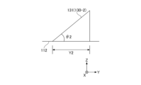
- FIG. 3A and 3B are enlarged views of the reflective surfaces 131 of the display device 100 according to an embodiment.
- Fig. 3A shows one of the reflective surfaces 131 of the reflector 130-1.
- Fig. 3B shows one of the reflective surfaces 131 of the reflector 130-2.
- reflecting section 130-1 is closer to light source 120 than reflecting section 130-2. For this reason, as shown in FIG. 3, the inclination angle ⁇ 1 of the multiple reflecting surfaces 131 of reflecting section 130-1 is set smaller than the inclination angle ⁇ 2 of the multiple reflecting surfaces 131 of reflecting section 130-2.
- the direction of the reflected light with the maximum light intensity is shifted from the vertical direction, and in one embodiment of the display device 100, the component of the amount of light reflected by the multiple reflective surfaces 131 in the direction of the symbol S1 (upward and vertical) (i.e., the light emitted from the display surface 111 to display the symbol S1) out of the light irradiated to the reflecting portion 130-1 can be reduced compared to when the direction of the reflected light with the maximum light intensity is vertical.
- the direction of reflected light with the greatest amount of light is vertical in the reflecting section 130-2 that is farthest from the light source 120, so that the amount of light reflected by the multiple reflecting surfaces 131 in the direction of the symbol S2 (upward and vertical) (i.e., the light emitted from the display surface 111 to display the symbol S2) can be increased among the light irradiated to the reflecting section 130-2.
- the amount of light is greatest in a specific direction and tends to decrease when it deviates from that direction.
- the direction in which the amount of light is greatest is the vertical direction, but in reflector 130-1, the tilt angle ⁇ 1 is set smaller than the tilt angle ⁇ 2 so that the direction in which the amount of light is greatest is shifted in the direction opposite to the light source.
- the amount of light irradiated to the reflecting portion 130-1 closer to the light source 120 is relatively large (the amount of attenuation is small due to the small number of total reflections) because it is closer to the light source 120, and the luminance of the symbol S1 would be relatively high if left as is.
- the luminance of the symbol S1 can be reduced to an appropriate level.
- the amount of light irradiated to the reflecting portion 130-2 farther from the light source 120 is relatively small (there is a large amount of attenuation due to the large number of total reflections) because of the distance from the light source 120, and as is, the luminance of the symbol S2 is relatively low.
- the luminance of the symbol S2 can be increased.
- the display device 100 of one embodiment it is possible to suppress the difference in brightness between the brightness of the symbol S1 and the brightness of the symbol S2 displayed on the display surface 111 of the light guide 110. Therefore, according to the display device 100 of one embodiment, it is possible to display a plurality of symbols on the display surface 111 of the light guide 110 so that the brightness is uniform, without adjusting the area of the reflective portion 130.
- the multiple reflective surfaces 131 provided on each of the reflecting sections 130-1 and 130-2 have the same inclination angle, but this is not limited thereto, and the multiple reflective surfaces 131 provided on any one of the reflecting sections 130-1 and 130-2 may have different inclination angles depending on the distance from the light source 120.
- the projected areas of the individual reflective surfaces 131 in the plan view from the display surface 111 side of the light guide 110 are equal among the multiple reflective sections 130 .
- the inclination angles of the reflecting surface 131 of the reflecting section 130-1 and the reflecting surface 131 of the reflecting section 130-2 are different, but the width Y1 in the left-right direction (Y-axis direction) of the reflecting surface 131 of the reflecting section 130-1 and the width Y2 in the left-right direction (Y-axis direction) of the reflecting surface 131 of the reflecting section 130-2 are equal to each other.
- the width in the front-back direction (X-axis direction) of the reflecting surface 131 of the reflecting section 130-1 and the width in the front-back direction (X-axis direction) of the reflecting surface 131 of the reflecting section 130-2 are equal to each other.
- the individual projected areas of the reflective surface 131 of the reflecting section 130-1 and the reflective surface 131 of the reflecting section 130-2 are equal to each other when viewed in a plan view from the display surface 111 side (positive side of the Z axis) of the light guide 110. Furthermore, the multiple reflective surfaces 131 of the reflecting section 130-1 and the multiple reflective surfaces 131 of the reflecting section 130-2 are arranged with equal spacing and equal density when viewed in a plan view from the display surface 111 side (positive side of the Z axis) of the light guide 110.
- the display device 100 of one embodiment when the light source 120 is not lit, the apparent brightness difference caused by the projected area of the reflective surface 131 of the symbol S1 and the symbol S2 displayed on the display surface 111 of the light guide 110 can be suppressed. That is, when the light source 120 is not lit, the reflective surface 131 reflects external light, and the surface of the reflective surface 131 may appear whitish. If the projected area of the reflective surface 131 is different in a plan view from the display surface 111 side (positive side of the Z axis) of the display surface 111, since each reflective surface 131 itself is very fine, it is almost impossible to see directly, but when the symbol is viewed as a whole, the apparent brightness appears different. However, according to the display device 100 of one embodiment, the projected area of each reflective surface 131 is equal between the multiple symbols displayed on the display surface 111 of the light guide 110, so that a user viewing the multiple symbols does not feel uncomfortable.
- the projected areas of the reflecting surfaces 131 of the reflecting sections 130-1 and 130-2 are equal, but instead, the actual areas of the reflecting surfaces 131 of the reflecting sections 130-1 and 130-2 may be equal. In this case, the projected areas of the reflecting surfaces 131 of the reflecting sections 130-1 and 130-2 will be different, but for example, by reducing the projected areas, it will be possible to achieve effects such as allowing the reflecting surfaces 131 to be arranged more closely together.
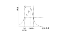
- FIG. 4 is a diagram showing the relationship between the inclination angle of the reflective surface 131 and the luminance of the symbol in the positive Z-axis direction (above and vertical to the symbol) in the display device 100 according to one embodiment, and shows the results obtained by simulation.
- the inclination angle of the reflective surface 131 is set for each of the multiple reflective sections 130-1, 130-2 so that the luminance of the multiple symbols displayed on the display surface 111 of the light guide 110 is equal.
- FIG. 4A is a graph showing the relationship between the inclination angle of the reflecting surface 131 of the reflecting unit 130-1 and the brightness of the symbol S1 displayed on the display surface 111.
- FIG. 4B is a graph showing the relationship between the inclination angle of the reflecting surface 131 of the reflecting unit 130-2 and the brightness of the symbol S2 displayed on the display surface 111.
- the inclination angle on the horizontal axis refers to the inclination angle of the reflecting surface 131 relative to the bottom surface 112.
- the inclination angle D21 at which the luminance of the symbol S2 is at its maximum is set as the inclination angle ⁇ 2 of the multiple reflecting surfaces 131.
- the inclination angle of the multiple reflective surfaces 131 of the reflective portion 130-2 (i.e., the reflective portion 130 furthest from the light source 120) is set so that maximum brightness is obtained when the symbol S2 corresponding to the reflective portion 130-2 is viewed from the display surface 111 side.
- the inclination angle D13 at which the luminance of the symbol S1 is equal to the luminance of the symbol S2 is set as the inclination angle ⁇ 1 of the multiple reflecting surfaces 131.
- the inclination of the curve showing the relationship between the inclination angle of the reflecting surface 131 and the brightness of the symbol S1 is greater for the inclination angle D11 than for the inclination angle D13. For this reason, even if the inclination angle deviates from the reference angle due to processing or installation, the effect on the change in brightness is smaller for the inclination angle D13.
- the light emitted from the light source 120 is directed toward the positive side of the Y axis, and when the inclination angle of the reflecting surface increases, the angle of incidence (angle of reflection) of the light on the reflecting surface tends to decrease, and when the angle of incidence is small, the light is emitted without being totally reflected, resulting in a large change in brightness.
- the angle of the reflecting surface decreases, the angle of reflection of the light on the reflecting surface tends to increase, and the totally reflected light maintains its totally reflected state, so the brightness does not change significantly.
- the display device 100 can easily make the luminance of the symbol S1 and the luminance of the symbol S2 displayed on the display surface 111 of the light guide 110 equal.
- the suitable inclination angles ⁇ 1 and ⁇ 2 of the reflecting surface 131 can be determined by a predetermined formula, simulation, etc.
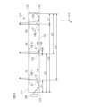
- Fig. 5 is a side view of a display device 100-2 according to the first modified example.
- the display device 100-2 has, as an example of the multiple reflectors 130, reflectors 130-1, 130-2, and 130-3, in that order from the light source 120 side (negative side of the Y axis).
- Reflector 130-1 displays symbol S1 on display surface 111 of light guide 110.
- Reflector 130-2 displays symbol S2 on display surface 111 of light guide 110.
- Reflector 130-3 displays symbol S3 on display surface 111 of light guide 110.
- Each of the reflecting sections 130-1, 130-2, and 130-3 has a plurality of reflecting surfaces 131 facing the first side surface 113 (negative side of the Y axis) on the bottom surface 112 of the light guide 110.
- FIG. 5 shows one representative of the plurality of reflecting surfaces 131 provided on the reflecting sections 130-1, 130-2, and 130-3.
- the light guide 110 has a side reflector 115 on the second side 114, which is the side opposite to the first side 113.
- the side reflector 115 is provided so as to cover the entire area of the second side 114.
- the side reflector 115 reflects the light irradiated to the second side 114, among the light propagating inside the light guide 110, to the inside of the light guide 110.
- the display device 100-2 according to the first modification can irradiate the reflectors 130-1, 130-2, and 130-3 with light from the second side 114 side (the positive side of the Y axis), thereby improving the brightness of each symbol on the display surface 111.
- an aluminum reflective sheet, a white reflective sheet, or white paint is used as the side reflector 115.
- the reflecting sections 130-1, 130-2, and 130-3 each have a second reflecting surface 132 formed integrally with each of the multiple reflecting surfaces 131, the second reflecting surface 132 facing the side reflecting section 115 (positive side of the Y axis).
- the reflecting portion 130 closer to the first side surface 113 is closer to the light source 120 and therefore the greater the amount of light irradiated from the first side surface 113 side (negative side of the Y-axis), but the amount of light reflected by the multiple reflecting surfaces 131 in the direction of the symbol (upward and vertically) (i.e., the light emitted from the display surface 111 to display the symbol) can be made relatively small.
- the inclination angle of the second reflecting surface 132 of the reflecting portion 130 relative to the bottom surface 112 of the light guide 110 becomes smaller the closer the reflecting portion 130 is to the side reflecting portion 115.
- the reflecting section 130-1 has a relatively large amount of light irradiated from the first side surface 113 (negative side of the Y-axis) because the distance L1 from the first side surface 113 is short, but because the inclination angle of the reflecting surface 131 with respect to the bottom surface 112 is relatively small, the amount of light reflected by the reflecting surface 131 in the direction of the symbol S1 (upward and vertically) can be relatively small, and therefore the brightness of the symbol S1 displayed on the display surface 111 can be made appropriate.
- the distance L3' from the side reflector 115 to the reflector 130-1 is long, the amount of light irradiated from the side reflector 115 side (positive side of the Y axis) is relatively small, but since the inclination angle of the second reflector 132 is relatively large, the amount of light reflected by the second reflector 132 in the direction of the symbol S1 (upward and vertically) can be relatively large, and therefore the brightness of the symbol S1 displayed on the display surface 111 can be made appropriate.
- the reflective section 130-2 has a medium distance L2 from the first side surface 113, and therefore the amount of light irradiated from the first side surface 113 (negative side of the Y-axis) is medium, but the inclination angle of the reflective surface 131 with respect to the bottom surface 112 is medium, and therefore the amount of light reflected by the reflective surface 131 in the direction of the symbol S2 (upward and vertically) can be medium, and therefore the brightness of the symbol S2 displayed on the display surface 111 can be made appropriate.
- the distance L2' from the side reflector 115 to the reflector 130-2 is medium, the amount of light irradiated from the side reflector 115 (positive side of the Y axis) is relatively medium, but since the inclination angle of the second reflector 132 is medium, the amount of light reflected by the second reflector 132 in the direction of the symbol S2 (upward and vertical) can be made medium, and therefore the brightness of the symbol S2 displayed on the display surface 111 can be made appropriate.
- the distance L3 from the first side surface 113 of the reflective section 130-3 is long, the amount of light irradiated from the first side surface 113 side (negative side of the Y-axis) is relatively small, but since the inclination angle of the reflective surface 131 with respect to the bottom surface 112 is relatively large, the amount of light reflected by the reflective surface 131 in the direction of the symbol S1 (upward and vertically) can be relatively large, and therefore the brightness of the symbol S3 displayed on the display surface 111 can be made appropriate.
- the distance L1' from the side reflector 115 to the reflector 130-3 is short, the amount of light irradiated from the side reflector 115 side (positive side of the Y axis) is relatively large, but since the inclination angle of the second reflector surface 132 is relatively small, the amount of light reflected by the second reflector surface 132 in the direction of the symbol S1 (upward and vertically) can be relatively small, and therefore the brightness of the symbol S3 displayed on the display surface 111 can be made appropriate.
- the display device 100 according to the first modified example can easily equalize the luminance of the symbols S1, S2, and S3 displayed on the display surface 111 of the light guide 110.
- the light guide 110 has a symmetrical structure in the left-right direction (Y-axis direction) in order to equalize the brightness of the symbols on the display surface 111 when the light source 120 is not lit.
- the distance L1 from the first side surface 113 of the reflecting portion 130-1 is equal to the distance L1' from the side surface reflecting portion 115 of the reflecting portion 130-3. Furthermore, the inclination angle of the reflecting surface 131 of the reflecting portion 130-1 is equal to the inclination angle of the second reflecting surface 132 of the reflecting portion 130-3. Furthermore, the inclination angle of the second reflecting surface 132 of the reflecting portion 130-1 is equal to the inclination angle of the reflecting surface 131 of the reflecting portion 130-3.
- the distance L2 from the first side surface 113 of the reflecting portion 130-2 is equal to the distance L2' from the side surface reflecting portion 115 of the reflecting portion 130-2. Furthermore, the inclination angle of the reflecting surface 131 of the reflecting portion 130-2 is equal to the inclination angle of the second reflecting surface 132 of the reflecting portion 130-2.
- the width W of the recess 133 formed by the adjacent reflective surface 131 and second reflective surface 132 is equal for reflective portions 130-1, 130-2, and 130-3. This allows the projection area of the recess 133 onto the XY plane to be the same. As a result, the size of the recess 133 can be made the same for all symbols, and the spacing (layout density) can be made constant, making it possible to keep the brightness of each symbol constant when the light source 120 is not lit.
- the reflective surface 131 and the second reflective surface 132 are configured to form a triangular shape (prism shape), but this is not limited thereto, and the reflective surface 131 and the second reflective surface 132 may be configured to form other shapes (e.g., a moon-cut shape, etc.).
- a second light source e.g., an LED
- the display device 100-2 according to the first modification can also irradiate the reflectors 130-1, 130-2, and 130-3 with light from the second side surface 114 side (the positive Y-axis side), thereby improving the brightness of each symbol on the display surface 111.
- the symbol S2 may be omitted, or a symbol may be added.
- Fig. 6 is a side view of a display device 100-3 according to the second modified example.
- the display device 100-3 according to the second modification is different from the display device 100-2 according to the first modification in that the upper end of the side reflector 115 is provided with an upper extension 115A that extends toward the first side 113 (negative Y-axis side) so as to cover part of the display surface 111, and the lower end of the side reflector 115 is provided with a lower extension 115B that extends toward the first side 113 (negative Y-axis side) so as to cover part of the bottom surface 112.
- the display device 100-3 of the second modified example is able to suppress leakage of light from the display surface 111 and bottom surface 112 by allowing the light reflected by the side reflecting portion 115 to be further reflected by the upper extension portion 115A and the lower extension portion 115B.
- the reflective surface may be formed by forming a convex portion that protrudes downward on the bottom surface of the light guide, rather than by forming a concave portion that is concave upward on the bottom surface of the light guide.
- the reflective surface may be formed by forming a concave portion that is recessed downward on the display surface (upper surface) of the light guide, or by forming a convex portion that protrudes upward on the display surface (upper surface) of the light guide.
Landscapes
- Physics & Mathematics (AREA)
- General Physics & Mathematics (AREA)
- Optics & Photonics (AREA)
- Engineering & Computer Science (AREA)
- Manufacturing & Machinery (AREA)
- General Engineering & Computer Science (AREA)
- Theoretical Computer Science (AREA)
- Instrument Panels (AREA)
- Illuminated Signs And Luminous Advertising (AREA)
Abstract
Description
図1は、一実施形態に係る表示装置100の平面図である。図2は、一実施形態に係る表示装置100の側面図である。図1および図2に示すように、表示装置100は、導光体110と、光源120とを備える。
以上のように構成された表示装置100は、光源120が駆動されて発光すると、光源120から発せられた光が、導光体110の第1の側面113から、導光体110内に入射される。導光体110内に入射された光の殆どは、導光体110内を全反射しながら伝搬する。
図3は、一実施形態に係る表示装置100が備える反射面131の拡大図である。図3Aは、反射部130-1が備える複数の反射面131のうちの一つを代表的に示す。図3Bは、反射部130-2が備える複数の反射面131のうちの一つを代表的に示す。
また、一実施形態に係る表示装置100においては、複数の反射部130の間で、導光体110の表示面111側からの平面視における、個々の反射面131の投影面積が等しくなっている。
図4は、一実施形態に係る表示装置100における、反射面131の傾斜角度とシンボルのZ軸正方向(シンボルの上方でかつ垂直方向)の輝度との関係を示す図であり、シュミレーションによって求めた結果を示す。
以下、図5を参照して、一実施形態に係る表示装置100の第1変形例を説明する。図5は、第1変形例に係る表示装置100-2の側面図である。
以下、図6を参照して、一実施形態に係る表示装置100の第2変形例を説明する。図6は、第2変形例に係る表示装置100-3の側面図である。
110 導光体
111 表示面
112 底面
113 第1の側面
114 第2の側面
115 側面反射部
115A 上側延長部
115B 下側延長部
120 光源
130,130-1,130-2,130-3 反射部
131 反射面
132 第2反射面
133 凹部
S1,S2,S3 シンボル
Claims (6)
- 光源と、
前記光源から発せられた光が第1の側面から入射される、透明且つ平板状の導光体と
を備え、
前記導光体は、
複数のシンボルに対応する複数の位置の各々に、底面に対して傾斜した複数の反射面からなる反射部を有し、
複数の前記反射部の各々が、前記複数の反射面によって前記第1の側面から入射された前記光を反射することにより、表示面に前記複数のシンボルを表示し、
前記反射部は、前記光源に近いほど、前記底面に対する前記反射面の傾斜角度が小さい
ことを特徴とする表示装置。 - 前記光源から最も遠い前記反射部は、
前記表示面側から当該反射部に対応するシンボルを視認したときに最大の輝度が得られるように、前記複数の反射面の傾斜角度が設定されている
ことを特徴とする請求項1に記載の表示装置。 - 前記表示面に表示される前記複数のシンボルの間で輝度が等しくなるように、複数の前記反射部の各々に対し、前記複数の反射面の前記傾斜角度が設定されている
ことを特徴とする請求項1に記載の表示装置。 - 複数の前記反射部の間で、前記表示面側からの平面視における、個々の前記反射面の投影面積が等しい
ことを特徴とする請求項1に記載の表示装置。 - 前記導光体は、
前記第1の側面とは反対側の第2の側面に側面反射部を有し、
複数の前記反射部の各々は、
前記複数の反射面の各々に対し、前記側面反射部側を向いた第2反射面が一体に形成されており、
前記反射部は、
前記側面反射部に近いほど、前記底面に対する前記第2反射面の傾斜角度が小さい
ことを特徴とする請求項1に記載の表示装置。 - 前記側面反射部は、
前記表示面の一部を覆うように、上端部から前記第1の側面側に延長された上側延長部と、
前記底面の一部を覆うように、下端部から前記第1の側面側に延長された下側延長部と
を有することを特徴とする請求項5に記載の表示装置。
Priority Applications (4)
| Application Number | Priority Date | Filing Date | Title |
|---|---|---|---|
| JP2024551344A JP7811277B2 (ja) | 2022-10-14 | 2023-09-15 | 表示装置 |
| CN202380070005.9A CN119968535A (zh) | 2022-10-14 | 2023-09-15 | 显示装置 |
| DE112023004296.9T DE112023004296T5 (de) | 2022-10-14 | 2023-09-15 | Displayvorrichtung |
| US19/173,161 US20250237802A1 (en) | 2022-10-14 | 2025-04-08 | Display device |
Applications Claiming Priority (2)
| Application Number | Priority Date | Filing Date | Title |
|---|---|---|---|
| JP2022-165543 | 2022-10-14 | ||
| JP2022165543 | 2022-10-14 |
Related Child Applications (1)
| Application Number | Title | Priority Date | Filing Date |
|---|---|---|---|
| US19/173,161 Continuation US20250237802A1 (en) | 2022-10-14 | 2025-04-08 | Display device |
Publications (1)
| Publication Number | Publication Date |
|---|---|
| WO2024080077A1 true WO2024080077A1 (ja) | 2024-04-18 |
Family
ID=90669099
Family Applications (1)
| Application Number | Title | Priority Date | Filing Date |
|---|---|---|---|
| PCT/JP2023/033678 Ceased WO2024080077A1 (ja) | 2022-10-14 | 2023-09-15 | 表示装置 |
Country Status (5)
| Country | Link |
|---|---|
| US (1) | US20250237802A1 (ja) |
| JP (1) | JP7811277B2 (ja) |
| CN (1) | CN119968535A (ja) |
| DE (1) | DE112023004296T5 (ja) |
| WO (1) | WO2024080077A1 (ja) |
Citations (3)
| Publication number | Priority date | Publication date | Assignee | Title |
|---|---|---|---|---|
| JPH07294745A (ja) * | 1994-04-25 | 1995-11-10 | Fanuc Ltd | バックライトパネル |
| JP2003519810A (ja) * | 2000-01-06 | 2003-06-24 | コーニンクレッカ フィリップス エレクトロニクス エヌ ヴィ | 照明装置及び発光パネル |
| JP2019053186A (ja) * | 2017-09-14 | 2019-04-04 | 株式会社ジャパンディスプレイ | 表示装置 |
Family Cites Families (6)
| Publication number | Priority date | Publication date | Assignee | Title |
|---|---|---|---|---|
| WO2000052667A1 (en) * | 1999-03-02 | 2000-09-08 | Matsushita Electric Industrial Co., Ltd. | Illuminating device and display device provided with the device |
| CN102997106A (zh) * | 2011-09-09 | 2013-03-27 | 柯尼卡美能达先进多层薄膜株式会社 | 照明装置以及照明台灯 |
| JP2014103049A (ja) * | 2012-11-21 | 2014-06-05 | Sony Corp | 光源デバイスおよび表示装置、ならびに電子機器 |
| JP6365115B2 (ja) * | 2014-08-25 | 2018-08-01 | オムロン株式会社 | 表示装置 |
| JP2017107048A (ja) * | 2015-12-09 | 2017-06-15 | オムロン株式会社 | 表示装置及び遊技機 |
| TWI755864B (zh) * | 2020-09-24 | 2022-02-21 | 誠屏科技股份有限公司 | 光源模組 |
-
2023
- 2023-09-15 JP JP2024551344A patent/JP7811277B2/ja active Active
- 2023-09-15 DE DE112023004296.9T patent/DE112023004296T5/de active Pending
- 2023-09-15 CN CN202380070005.9A patent/CN119968535A/zh active Pending
- 2023-09-15 WO PCT/JP2023/033678 patent/WO2024080077A1/ja not_active Ceased
-
2025
- 2025-04-08 US US19/173,161 patent/US20250237802A1/en active Pending
Patent Citations (3)
| Publication number | Priority date | Publication date | Assignee | Title |
|---|---|---|---|---|
| JPH07294745A (ja) * | 1994-04-25 | 1995-11-10 | Fanuc Ltd | バックライトパネル |
| JP2003519810A (ja) * | 2000-01-06 | 2003-06-24 | コーニンクレッカ フィリップス エレクトロニクス エヌ ヴィ | 照明装置及び発光パネル |
| JP2019053186A (ja) * | 2017-09-14 | 2019-04-04 | 株式会社ジャパンディスプレイ | 表示装置 |
Also Published As
| Publication number | Publication date |
|---|---|
| US20250237802A1 (en) | 2025-07-24 |
| JP7811277B2 (ja) | 2026-02-04 |
| CN119968535A (zh) | 2025-05-09 |
| DE112023004296T5 (de) | 2025-08-14 |
| JPWO2024080077A1 (ja) | 2024-04-18 |
Similar Documents
| Publication | Publication Date | Title |
|---|---|---|
| US6139163A (en) | Planar light source unit | |
| JP6220152B2 (ja) | 表示装置 | |
| CN101295042B (zh) | 背光模组及其光学板 | |
| CN101295040B (zh) | 背光模组及其光学板 | |
| TW201430462A (zh) | 面光源裝置 | |
| CN104062803B (zh) | 显示装置的背光单元 | |
| JP2015014789A (ja) | 光学レンズ、発光装置及び表示装置 | |
| JP4140710B2 (ja) | 表示装置 | |
| CN102588766A (zh) | 发光装置和图像显示设备 | |
| JP2013012380A (ja) | 光束制御部材、この光束制御部材を備えた発光装置およびこの発光装置を備えた面光源装置 | |
| US8390470B2 (en) | Display device | |
| JP4708440B2 (ja) | 面光源装置 | |
| JP4485999B2 (ja) | 面光源装置 | |
| JP7811277B2 (ja) | 表示装置 | |
| CN110291328A (zh) | 光束控制部件、发光装置及面光源装置 | |
| TWI722799B (zh) | 面光源裝置及液晶顯示裝置 | |
| JP7238551B2 (ja) | 表示装置及び画像形成装置 | |
| JP7606938B2 (ja) | ヘッドアップディスプレイ及び表示装置 | |
| KR101732020B1 (ko) | 백라이트 유닛 및 이를 포함하는 표시 장치 | |
| KR20120085181A (ko) | 도광판 및 면광원 장치 | |
| JP7504590B2 (ja) | 面光源装置および表示装置 | |
| JP2024006330A (ja) | 面光源装置および表示装置 | |
| JP6820778B2 (ja) | 光束制御部材、発光装置および面光源装置 | |
| JPWO2017154841A1 (ja) | 面状発光モジュール及び照明装置 | |
| WO2020196572A1 (ja) | 面光源装置および表示装置 |
Legal Events
| Date | Code | Title | Description |
|---|---|---|---|
| 121 | Ep: the epo has been informed by wipo that ep was designated in this application |
Ref document number: 23877083 Country of ref document: EP Kind code of ref document: A1 |
|
| WWE | Wipo information: entry into national phase |
Ref document number: 202380070005.9 Country of ref document: CN |
|
| WWE | Wipo information: entry into national phase |
Ref document number: 2024551344 Country of ref document: JP |
|
| WWP | Wipo information: published in national office |
Ref document number: 202380070005.9 Country of ref document: CN |
|
| WWE | Wipo information: entry into national phase |
Ref document number: 112023004296 Country of ref document: DE |
|
| WWP | Wipo information: published in national office |
Ref document number: 112023004296 Country of ref document: DE |
|
| 122 | Ep: pct application non-entry in european phase |
Ref document number: 23877083 Country of ref document: EP Kind code of ref document: A1 |