WO2024162000A1 - Dispositif de détection de lumière et appareil électronique - Google Patents
Dispositif de détection de lumière et appareil électronique Download PDFInfo
- Publication number
- WO2024162000A1 WO2024162000A1 PCT/JP2024/001099 JP2024001099W WO2024162000A1 WO 2024162000 A1 WO2024162000 A1 WO 2024162000A1 JP 2024001099 W JP2024001099 W JP 2024001099W WO 2024162000 A1 WO2024162000 A1 WO 2024162000A1
- Authority
- WO
- WIPO (PCT)
- Prior art keywords
- polarization
- additional
- light
- polarized light
- unit
- Prior art date
- Legal status (The legal status is an assumption and is not a legal conclusion. Google has not performed a legal analysis and makes no representation as to the accuracy of the status listed.)
- Ceased
Links
Images















Classifications
-
- G—PHYSICS
- G02—OPTICS
- G02B—OPTICAL ELEMENTS, SYSTEMS OR APPARATUS
- G02B5/00—Optical elements other than lenses
- G02B5/30—Polarising elements
-
- H—ELECTRICITY
- H10—SEMICONDUCTOR DEVICES; ELECTRIC SOLID-STATE DEVICES NOT OTHERWISE PROVIDED FOR
- H10F—INORGANIC SEMICONDUCTOR DEVICES SENSITIVE TO INFRARED RADIATION, LIGHT, ELECTROMAGNETIC RADIATION OF SHORTER WAVELENGTH OR CORPUSCULAR RADIATION
- H10F39/00—Integrated devices, or assemblies of multiple devices, comprising at least one element covered by group H10F30/00, e.g. radiation detectors comprising photodiode arrays
- H10F39/10—Integrated devices
- H10F39/12—Image sensors
Definitions
- This disclosure relates to a light detection device and an electronic device.
- a polarized image sensor (light detection device) equipped with a polarizer can obtain, in addition to brightness and color information, polarization information that cannot be detected by image sensors without polarizers, and it is also possible to grasp the shape of the subject from such polarization information. For this reason, polarized image sensors can be used in the inspection of objects that are difficult to visualize or recognize using images output by image sensors without polarizers, and it is expected that they will continue to be used in a variety of industrial equipment fields.
- Patent Document 1 discloses a solid-state imaging element that includes a wire-grid polarizer and a photoelectric conversion element.
- polarized waves of incident light that pass through a wire-grid polarizer enter a photoelectric conversion element (light-receiving pixel) and are received.
- a wire-grid polarizer transmits only polarized light that vibrates in a desired direction from the incident light and blocks polarized light that vibrates in other directions, resulting in large optical losses and low light transmittance.
- solid-state imaging elements equipped with wire-grid polarizers tend to exhibit low sensitivity and low extinction ratios.
- polarizers with metasurface structures tend to exhibit superior light transmittance compared to wire-grid polarizers.
- each light-receiving pixel receives not only polarized light that vibrates in the desired direction, but also polarized light that vibrates in a direction different from the desired direction, making it difficult to achieve a good extinction ratio.
- the present disclosure provides a technology that is advantageous in suppressing reception of undesired polarized light while achieving good sensitivity to the desired polarized light in each light receiving pixel.
- a light detection device that includes a polarization control unit that includes a plurality of microstructures arranged two-dimensionally and selectively transmits a plurality of polarized light beams in incident light, an additional polarizer that receives the plurality of polarized light beams from the polarization control unit and selectively transmits the plurality of polarized light beams, and a photoelectric conversion unit that includes a plurality of light receiving pixels that receive the plurality of polarized light beams from the additional polarizer, and the plurality of polarized light beams that transmit each of the polarization control unit and the additional polarizer include a first polarized light beam, a second polarized light beam, a third polarized light beam, and a fourth polarized light beam that have mutually different vibration directions.
- the polarization control unit may focus each of the multiple polarized lights toward different regions of the additional polarizer.
- the additional polarizer may include a wire grid polarizer.
- the additional polarizer may include a photonic crystal polarizer.
- the additional polarizer may include a plurality of additional polarization pixels and an additional polarization shielding portion provided between adjacent additional polarization pixels, and each of the plurality of additional polarization pixels may selectively transmit any one of the first polarization, the second polarization, the third polarization, and the fourth polarization.
- the first polarized light and the second polarized light may have vibration directions that differ by 90 degrees from each other
- the third polarized light and the fourth polarized light may have vibration directions that differ by 90 degrees from each other
- the second polarized light and the third polarized light may have vibration directions that differ by 45 degrees from each other.
- the polarization control unit may include a first unit polarization control unit that selectively transmits the first polarized light and the second polarized light, and a second unit polarization control unit that selectively transmits the third polarized light and the fourth polarized light
- the additional polarizer may include a plurality of additional polarization pixels that selectively transmit any of the first polarized light, the second polarized light, the third polarized light, and the fourth polarized light
- the first unit polarization control unit may focus the first polarized light toward the additional polarization pixels that selectively transmit the first polarized light and focus the second polarized light toward the additional polarization pixels that selectively transmit the second polarized light
- the second unit polarization control unit may focus the third polarized light toward the additional polarization pixels that selectively transmit the third polarized light and focus the fourth polarized light toward the additional polarization pixels that selectively transmit the fourth polarized light.
- the optical detection device may include a waveguide provided between the polarization control unit and the additional polarizer, and the waveguide may have a first unit polarization waveguide through which the first and second polarized lights output from the first unit polarization control unit travel toward the additional polarizer, and a second unit polarization waveguide through which the third and fourth polarized lights output from the second unit polarization control unit travel toward the additional polarizer, and a polarization control light shielding unit may be provided between adjacent first and second unit polarization waveguides.
- the polarization control light blocking portion may include a metal.
- the polarization control light blocking portion may include an air layer.
- the multiple light receiving pixels may have a diagonal lattice arrangement.
- the additional polarizer may include a number of additional polarizing pixels having a diagonal grid arrangement.
- the polarization control unit may include multiple unit polarization control units having a diagonal grid arrangement.
- Another aspect of the present disclosure relates to an electronic device that includes any of the above-mentioned photodetection devices.
- FIG. 1 is a schematic diagram showing an example of the configuration of an image sensor.
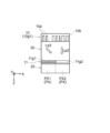
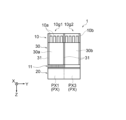
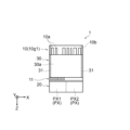
- FIG. 2A is a partial cross-sectional view (XZ cross-sectional view) illustrating an outline of an image sensor of a first example of the first embodiment.
- FIG. 2B is a partial cross-sectional view (XZ cross-sectional view) illustrating an outline of an image sensor of a first example of the first embodiment.
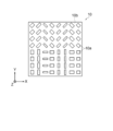
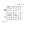
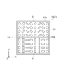
- FIG. 3 is a plan view showing an outline of the polarization control section (particularly the polarization control unit) of the first example of the first embodiment.
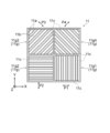
- FIG. 4 is a plan view showing an outline of an additional polarizer (particularly an additional polarizing pixel unit) of a first example of the first embodiment.
- FIG. 5 is a plan view of a polarization control section (particularly a polarization control unit) showing an example of a unit polarization control section.
- FIG. 6 is a plan view of an additional polarizer (particularly an additional polarization pixel unit) illustrating the correspondence between the additional polarization pixels of the additional polarizer shown in FIG. 4 and the vibration directions of the assigned polarization.
- FIG. 9 is a plan view showing an outline of a modified example of an additional polarizer.
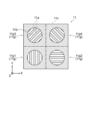
- FIG. 10 is a diagram showing an example of the results (received light power distribution) of a wave simulation by the FDTD method in a photoelectric conversion section (particularly a light receiving pixel unit including the first to fourth light receiving pixels).
- FIG. 11 is a plan view showing an outline of a polarization control section (particularly, a polarization control unit) of a second example of the first embodiment.
- FIG. 12 is a plan view illustrating an outline of an additional polarizer (particularly an additional polarization pixel unit) according to a second example of the first embodiment.
- FIG. 13 is a plan view showing an outline of a polarization control section (particularly, a polarization control unit) according to a third example of the first embodiment.
- FIG. 14 is a plan view illustrating an outline of an additional polarizer (particularly an additional polarization pixel unit) according to a third example of the first embodiment.
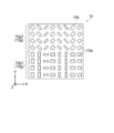
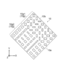
- FIG. 15 is a plan view showing an outline of a polarization control section (particularly, a polarization control unit) according to a fourth example of the first embodiment.
- FIG. 13 is a plan view showing an outline of a polarization control section (particularly, a polarization control unit) according to a third example of the first embodiment.
- FIG. 14 is a plan view showing an outline of a polarization control section (particularly, a polarization control unit) according to a fourth example of the first embodiment.
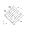
- FIG. 16 is a plan view illustrating an outline of an additional polarizer (particularly an additional polarization pixel unit) according to a fourth example of the first embodiment.
- FIG. 17 is a plan view showing an outline of a polarization control section (particularly, a polarization control unit) according to a fifth example of the first embodiment.
- FIG. 18 is a plan view illustrating an outline of an additional polarizer (particularly an additional polarization pixel unit) according to a fifth example of the first embodiment.
- FIG. 19 is a plan view showing an outline of a polarization control section (particularly, a polarization control unit) according to a sixth example of the first embodiment.
- FIG. 17 is a plan view showing an outline of a polarization control section (particularly, a polarization control unit) according to a fifth example of the first embodiment.
- FIG. 20 is a plan view illustrating an outline of an additional polarizer (particularly an additional polarization pixel unit) according to a sixth example of the first embodiment.
- FIG. 21 is a schematic plan view illustrating a portion of a photoelectric conversion unit including light-receiving pixels arranged in a square lattice.
- FIG. 22 is a schematic plan view illustrating a portion of a photoelectric conversion unit including light receiving pixels arranged in a diagonal lattice.
- FIG. 21 is a schematic plan view illustrating a portion of a photoelectric conversion unit including light-receiving pixels arranged in a square lattice.
- FIG. 22 is a schematic plan view illustrating a portion of a photoelectric conversion unit including light receiving pixels arranged in a diagonal lat
- FIG. 25 is a plan view of a polarization control section (particularly a polarization control unit) showing an example of a unit polarization control section of the first example of the second embodiment.
- FIG. 26 is a plan view illustrating an outline of an additional polarizer (particularly an additional polarization pixel unit) of a first example of the second embodiment.
- FIG. 27 is a perspective view illustrating an outline of an additional polarizer of a first example of the second embodiment.
- FIG. 28 is a plan view showing an outline of a polarization control section (particularly, a polarization control unit) of a second example of the second embodiment.
- FIG. 29 is a plan view illustrating an outline of an additional polarizer (particularly an additional polarization pixel unit) of a second example of the second embodiment.
- FIG. 30 is a plan view showing an outline of a polarization control section (particularly a polarization control unit) of a third example of the second embodiment.
- FIG. 31 is a plan view illustrating an outline of an additional polarizer (particularly an additional polarization pixel unit) of a third example of the second embodiment.
- FIG. 32 is a plan view showing an outline of a polarization control section (particularly a polarization control unit) of a fourth example of the second embodiment.
- FIG. 33 is a plan view illustrating an outline of an additional polarizer (particularly an additional polarization pixel unit) of a fourth example of the second embodiment.
- FIG. 34 is a plan view showing an outline of a polarization control section (particularly, a polarization control unit) of a fifth example of the second embodiment.
- FIG. 35 is a plan view illustrating an outline of an additional polarizer (particularly an additional polarization pixel unit) of a fifth example of the second embodiment.
- FIG. 36 is a plan view showing an outline of a polarization control section (particularly a polarization control unit) of a sixth example of the second embodiment.
- FIG. 37 is a plan view illustrating an outline of an additional polarizer (particularly an additional polarization pixel unit) of a sixth example of the second embodiment.
- FIG. 38 is a plan view of a polarization control section showing a first modified example of an image sensor.
- 39 is a cross-sectional view showing an example of the YZ plane of the image sensor shown in FIG.
- FIG. 40 is a cross-sectional view showing an example of the XZ plane of the image sensor shown in FIG. FIG.
- FIG. 41 is a cross-sectional view for explaining an example of a method for manufacturing an image sensor (particularly, an image sensor including a wire-grid type additional polarizer).
- FIG. 42 is a cross-sectional view illustrating an example of a manufacturing method for an image sensor (particularly, an image sensor including a wire-grid type additional polarizer).
- FIG. 43 is a cross-sectional view illustrating an example of a manufacturing method for an image sensor (particularly, an image sensor including a wire-grid type additional polarizer).
- FIG. 44 is a cross-sectional view illustrating an example of a manufacturing method for an image sensor (particularly, an image sensor including a wire-grid type additional polarizer).
- FIG. 45 is a cross-sectional view illustrating an example of a manufacturing method for an image sensor (particularly, an image sensor including a wire-grid type additional polarizer).
- FIG. 46 is a cross-sectional view illustrating an example of a manufacturing method for an image sensor (particularly, an image sensor including a wire-grid type additional polarizer).
- FIG. 47 is a cross-sectional view illustrating an example of a manufacturing method for an image sensor (particularly, an image sensor including a wire-grid type additional polarizer).
- FIG. 48 is a cross-sectional view illustrating an example of a manufacturing method for an image sensor (particularly, an image sensor including a wire-grid type additional polarizer).
- each element in the drawings is shown diagrammatically or conceptually. Therefore, the characteristics of each element in the drawings, such as the size and shape, may differ from the characteristics of the corresponding element in reality. Furthermore, the size ratios between elements in the drawings may differ from the size ratios between corresponding elements in the actual device. Furthermore, the size and shape of each element and the size ratios between elements do not necessarily match between drawings, and one or more specific elements may be exaggerated in each drawing.
- the X, Y, and Z directions are mutually perpendicular.
- the X direction may correspond to the horizontal direction
- the Y direction may correspond to the vertical direction (height direction)
- the Z direction may correspond to the depth direction.
- FIG. 1 is a schematic diagram showing an example of the configuration of an image sensor 1.
- the polarization control unit (polarization splitter) 10, additional polarizer 11, and photoelectric conversion unit 20 are shown as viewed from an angle, and the optical system OP is shown as viewed from the side.
- Image sensor 1 can typically be configured as a CCD (Charge Coupled Device) image sensor or a CMOS (Complementary Metal Oxide Semiconductor) image sensor. However, image sensor 1 can be configured as any imaging device.
- CCD Charge Coupled Device
- CMOS Complementary Metal Oxide Semiconductor
- the image sensor 1 receives light from an external subject, acquires data on various pieces of information including the intensity and color of the light, and generates an image of the subject.
- the polarization information of the light from the subject contains useful information that cannot be acquired from the light intensity and color (wavelength) alone, and may include, for example, information on the shape of the subject's surface and information on the material of the subject. Polarized imaging technology that uses such polarization information can be used in a variety of fields, such as in-vehicle cameras, IoT (Internet of Things) devices, and medical devices.
- the image sensor 1 shown in FIG. 1 includes an optical system OP, a polarization control unit 10, an additional polarizer 11, and a photoelectric conversion unit 20.
- the optical system OP includes a lens that collects incident light L from a subject.
- the incident light L that passes through the optical system OP includes frontal incident light La that travels in the optical axis direction of the principal ray, and oblique incident light Lb that travels in a direction oblique to the optical axis of the principal ray.
- the optical axis direction coincides with the Z direction.
- the photoelectric conversion unit 20 includes a number of light-receiving pixels PX that receive incident light L (particularly a number of polarized lights extracted from the incident light L).
- the multiple light-receiving pixels PX are arranged two-dimensionally in the X and Y directions, and the photoelectric conversion unit 20 as a whole has a rectangular shape with sides extending in the X and Y directions.
- the light-receiving pixel PX located at the center of the photoelectric conversion unit 20 (0% image height) receives frontal incident light La.
- the light-receiving pixel PX located away from the center of the photoelectric conversion unit 20 receives oblique incident light Lb.
- Each light-receiving pixel PX has a photodiode made of a Si (silicon) semiconductor material or the like. Note that the light absorption coefficient of each light-receiving pixel PX is not necessarily large, since the absorption rate (sensitivity) of the incident light can change depending on the wavelength (e.g., 940 nm) of the incident light (polarized light). Therefore, as an example, a light scatterer (not shown) may be placed on the surface (light-receiving surface) of each light-receiving pixel PX to scatter the incident light, thereby increasing the optical path length of the incident light at each light-receiving pixel PX and improving the sensitivity of each light-receiving pixel PX.
- a light scatterer may be placed on the surface (light-receiving surface) of each light-receiving pixel PX to scatter the incident light, thereby increasing the optical path length of the incident light at each light-receiving pixel PX and improving the sensitivity
- the polarization control unit 10 and the additional polarizer 11 are disposed in the optical path between the optical system OP and the photoelectric conversion unit 20, and are arranged to cover the multiple light receiving pixels PX (particularly the light receiving surfaces) of the photoelectric conversion unit 20.
- the polarization control unit 10 has a metasurface structure including a large number (multiple) of microstructures also called "meta-atoms".
- the additional polarizer 11 is a polarizer that does not have a metasurface structure.
- the additional polarizer 11 it is possible to use a polarizer of any structure (for example, a wire grid type polarizer or a photonic crystal type polarizer described below) that can extract the desired linearly polarized light from the incident light L.
- the polarization control unit 10 and the additional polarizer 11 in the portions covering the light-receiving pixels PX located in the center of the photoelectric conversion unit 20 perform polarization control of the frontal incident light La, and focus the frontal incident light La (particularly the polarized component) on the light-receiving pixels PX located in the center of the photoelectric conversion unit 20.
- the polarization control unit 10 and the additional polarizer 11 in the portions covering the light-receiving pixels PX located at the ends of the photoelectric conversion unit 20 perform polarization control of the oblique incident light Lb, and focus the oblique incident light Lb (particularly the polarized component) on the light-receiving pixels PX located at the ends of the photoelectric conversion unit 20. In this way, each portion of the polarization control unit 10 and the additional polarizer 11 selectively passes specific polarized components contained in the incident light L incident at various angles, and focuses them on the corresponding light-receiving pixels PX.
- the additional polarizer 11 is disposed between the polarization control unit 10 and the photoelectric conversion unit 20 in the optical axis direction, and receives multiple polarized light from the polarization control unit 10 and selectively transmits the multiple polarized light.
- the polarization control unit 10 focuses the multiple polarized light toward different regions of the additional polarizer 11 (multiple additional polarization pixels described below), as described below.
- the multiple light-receiving pixels PX of the photoelectric conversion unit 20 receive the multiple polarized light selectively emitted from the additional polarizer 11.
- a polarization control unit 10 (particularly a unit polarization control unit described below) and an additional polarizer 11 (particularly an additional polarization pixel described below) are assigned to each light-receiving pixel PX so that polarized light vibrating in the desired direction is selectively incident thereon.
- the multiple polarized lights that are transmitted through the polarization control unit 10 and the additional polarizer 11 and received by the photoelectric conversion unit 20 include a first polarized light, a second polarized light, a third polarized light, and a fourth polarized light that have different vibration directions.
- the specific vibration directions of the first to fourth polarized light are not limited.
- the first and second polarized light have vibration directions that differ by 90 degrees from each other
- the third and fourth polarized light have vibration directions that differ by 90 degrees from each other
- the second and third polarized light have vibration directions that differ by 45 degrees from each other.
- the first to fourth polarized light have vibration directions of 0 degrees, +90 degrees, -45 degrees, and +45 degrees based on the propagation direction, respectively.
- the vibration direction of 0 degrees may be a direction that coincides with the X direction
- the vibration direction of +90 degrees may be a direction that coincides with the Y direction
- the vibration directions of -45 degrees and +45 degrees may be directions that are oblique to the X direction and the Y direction.
- the image sensor 1 (particularly the polarization control unit 10 and the additional polarizer 11) described above can have various configurations. A typical embodiment of the image sensor 1 will be described below.
- the additional polarizer 11 in this embodiment includes a wire grid type polarizer.
- FIG. 2A and 2B are partial cross-sectional views (XZ cross-sectional views) showing an outline of the image sensor 1 of the first example of the first embodiment, and show the case where the incident light L is perpendicularly incident on the image sensor 1 (particularly the polarization control unit 10).
- FIG. 2A shows the first light receiving pixel PX1 and the second light receiving pixel PX2
- FIG. 2B shows the third light receiving pixel PX3 and the fourth light receiving pixel PX4.
- FIG. 3 is a plan view showing an outline of the polarization control unit 10 (particularly the polarization control unit) of the first example of the first embodiment.
- FIG. 4 is a plan view showing an outline of the additional polarizer 11 (particularly the additional polarization pixel unit) of the first example of the first embodiment.
- FIG. 5 is a plan view of the polarization control unit 10 (particularly the polarization control unit) showing an example of a unit polarization control unit 10g.
- FIG. 6 is a plan view of the additional polarizer 11 (particularly the additional polarization pixel unit) showing the correspondence between the additional polarization pixels 11g of the additional polarizer 11 shown in FIG. 4 and the vibration directions P1 to P4 of the assigned polarization.
- the polarization control unit 10, the additional polarizer 11, and the photoelectric conversion unit 20 each have a square pixel array.
- four light receiving pixels PX arranged in a square lattice arrangement with two light receiving pixels PX lined up in the X direction and two light receiving pixels PX lined up in the Y direction, form one light receiving pixel unit, and multiple such light receiving pixel units are arranged in the X direction and Y direction.
- the four light receiving pixels PX (first light receiving pixel PX1 to fourth light receiving pixel PX4) included in each light receiving pixel unit are assigned to the first polarization Lp1 to fourth polarization Lp4, respectively (see Figures 2A and 2B).
- the phase of the polarization information acquired by the image sensor 1, which is capable of separating and receiving polarized light vibrating in four directions, makes it possible to estimate the normal vector of the subject's surface, and thus to grasp the shape of the subject.
- the additional polarizer 11 which is a wire grid polarizer, includes a large number of wires 11a (see FIG. 4).
- Each wire 11a is made of a metal such as aluminum (Al), but may be made of other materials.
- the inter-wire portions 11b between adjacent wires 11a are polarized light transmitting regions, and may be configured as spaces (air regions) or may be configured of a low refractive index material (for example, silicon dioxide (SiO 2 )).
- a low refractive index material for example, silicon dioxide (SiO 2 )
- the additional polarizer 11 is divided into a number of additional polarization pixels 11g as shown in FIG. 4.
- the multiple additional polarization pixels 11g included in the additional polarizer 11 in this example have a square lattice arrangement.
- four additional polarization pixels 11g arranged in a square lattice arrangement with two additional polarization pixels 11g arranged in the X direction and two additional polarization pixels 11g arranged in the Y direction, constitute one additional polarization pixel unit, and multiple such additional polarization pixel units are arranged in the X direction and Y direction.
- These four additional polarization pixels 11g included in each additional polarization pixel unit are assigned to the first polarization Lp1 to the fourth polarization Lp4, respectively.
- each additional polarization pixel 11g selectively transmits one of the first polarization Lp1, the second polarization Lp2, the third polarization Lp3, and the fourth polarization Lp4.
- the extension direction of the wire line 11a of each additional polarization pixel 11g is determined according to the vibration direction of the assigned polarization, and is a direction that forms an angle of 90 degrees with respect to the vibration direction of the assigned polarization (see FIG. 6).
- the additional polarizer 11 further has a frame-shaped additional polarizing light-shielding portion 11c (see FIG. 4) that is arranged to surround each additional polarizing pixel 11g.
- the additional polarizing light-shielding portion 11c has any configuration and any composition that can block the transmission of light (particularly polarized light). Therefore, the additional polarizing light-shielding portion 11c may be configured to block light by reflecting light, or may be configured to block light by absorbing light.
- the additional polarized light shielding portion 11c thus provided between adjacent additional polarized pixels 11g can suppress leakage (crosstalk) of light (especially polarized light) between adjacent additional polarized pixels 11g, which is advantageous for obtaining a high extinction ratio.
- the polarization control unit 10 of the metasurface structure is provided upstream of the additional polarizer 11 in the incident direction A0 of the incident light L.
- This polarization control unit 10 exhibits a polarization splitter function that selectively transmits and separates multiple polarized lights (first polarized light Lp1 to fourth polarized light Lp4) in the incident light L.
- a waveguide 30 is provided between the polarization control unit 10 and the photoelectric conversion unit 20 (each light receiving pixel PX).
- the waveguide 30 can have any configuration, and the material that can be used to form the waveguide 30 is not limited.
- the waveguide 30 may be made of any transparent material selected from the group consisting of amorphous silicon, polycrystalline silicon, germanium, titanium oxide, niobium oxide, tantalum oxide, aluminum oxide, hafnium oxide, silicon nitride, silicon oxide, silicon nitride oxide, silicon carbide, silicon oxide carbide, silicon nitride carbide, and zirconium oxide.
- the multiple meta-atoms (microstructures) 10a included in the polarization control unit 10 are arranged two-dimensionally in the X and Y directions as shown in FIG. 3, and are arranged in a plane that is approximately parallel to the light receiving surface of the light receiving pixel PX (photoelectric conversion unit 20).
- the refractive index of each meta-atom 10a is greater than the refractive index of the area between the meta-atoms 10a (i.e., the peripheral portion 10b of the structure).
- each meta-atom 10a may have any configuration, and the material that can form each meta-atom 10a is not limited.
- each meta-atom 10a may be made of any of amorphous silicon ( ⁇ -Si), polycrystalline silicon (Poly-Si), germanium, titanium oxide (TiO 2 ), niobium oxide, tantalum oxide, aluminum oxide, hafnium oxide, silicon nitride (SiN, Si 3 N 4 ), silicon oxide, silicon nitride oxide, silicon carbide, silicon oxide carbide, silicon nitride carbide, zirconium oxide, gallium nitride (GaN), gallium arsenide (GaAs), and indium phosphide (InP).
- ⁇ -Si amorphous silicon
- Poly-Si polycrystalline silicon
- germanium titanium oxide
- TiO 2 titanium oxide
- niobium oxide tantalum oxide
- aluminum oxide hafnium oxide
- silicon nitride SiN, Si 3 N 4
- the regions between the meta-atoms 10a can have any configuration, for example they can be provided as spaces or can be made of a solid material such as silicon dioxide.
- the meta-atom 10a and the waveguide 30 are made of different materials.
- the waveguide 30 is made of silicon oxide film or titanium oxide
- the meta-atom 10a may be made of single crystal silicon or amorphous silicon.
- the peripheral portion 10b of the structure may be made of a material different from that of the waveguide 30, or may be made of the same material as the waveguide 30.
- Each meta atom 10a has a pillar shape, and is ideally configured as a rectangular parallelepiped with a rectangular cross-sectional shape and planar shape. In reality, however, when the polarization control unit 10 is fabricated by processing using a lithography photomask, the corners of each meta atom 10a may be rounded. Even if the corners of each meta atom 10a are rounded, the polarization control unit 10 can fully function as a polarization splitter. In this way, the shape of each meta atom 10a is not limited, and the cross-sectional shape and planar shape of each meta atom 10a may be any polygonal, elliptical, hollow, or other shape.
- the polarization control unit 10 includes multiple types of unit polarization control units 10g that separate and emit (focus) polarized light that vibrates in different directions (see Figure 5).
- Each unit polarization control unit 10g in this example is provided in a range corresponding to two light-receiving pixels PX (i.e., an area covering two light-receiving pixels PX), and selectively emits two polarized components in the incident light L in directions different from each other to focus the light. This enables each unit polarization control unit 10g to focus polarized light that is incident on a range corresponding to two pixels (multiple pixels) of the incident light L onto the additional polarizer 11 (additional polarization pixel 11g) and photoelectric conversion unit 20 (light-receiving pixel PX) that correspond to one pixel (single pixel).
- the multiple unit polarization control units 10g include a first unit polarization control unit 10g1 and a second unit polarization control unit 10g2.
- one first unit polarization control unit 10g1 and one second unit polarization control unit 10g2 adjacent in the Y direction are considered as one polarization control unit, and multiple such polarization control units are arranged in the X and Y directions.
- the first unit polarization control unit 10g1 is assigned to the first additional polarization pixel 11g1 and the second additional polarization pixel 11g2, and is therefore assigned to the first light receiving pixel PX1 and the second light receiving pixel PX2.
- the second unit polarization control unit 10g2 is assigned to the third additional polarization pixel 11g3 and the fourth additional polarization pixel 11g4, and is therefore assigned to the third light receiving pixel PX3 and the fourth light receiving pixel PX4.
- the multiple meta atoms 10a included in each first unit polarization control unit 10g1 are linearly arranged along each of the vibration direction P1 (0 degrees: X direction) of the first polarized light Lp1 and the vibration direction P2 (90 degrees: Y direction) of the second polarized light Lp2 in the incident light L.
- the multiple meta atoms 10a of each first unit polarization control unit 10g1 include multiple meta atoms 10a whose sizes are different from each other in the vibration direction P1 (X direction) of the first polarized light Lp1 and the vibration direction P2 (Y direction) of the second polarized light Lp2 in the incident light L.
- each second unit polarization control unit 10g2 are linearly arranged along the vibration direction P3 (-45 degrees) of the third polarization Lp3 and the vibration direction P4 (+45 degrees) of the fourth polarization Lp4, and include multiple meta atoms 10a whose sizes in the vibration directions P3 and P4 are different from each other.
- each unit polarization control unit 10g selectively emits (focuses) the polarized components in the incident light L toward the additional polarizer 11 (particularly the corresponding additional polarization pixel 11g).
- the first unit polarization control unit 10g1 selectively transmits the first polarized light Lp1 and the second polarized light Lp2 in the incident light L, and outputs (concentrates) the first polarized light Lp1 toward the first additional polarization pixel 11g1 while outputting (concentrates) the second polarized light Lp2 toward the second additional polarization pixel 11g2.
- the traveling direction of the first polarized light Lp1 from the first unit polarization control unit 10g1 toward the first additional polarization pixel 11g1 is represented by "A1”.
- the traveling direction of the second polarized light Lp2 from the first unit polarization control unit 10g1 toward the second additional polarization pixel 11g2 is represented by "A2".
- the first polarized light Lp1 emitted from the portion of the first unit polarization control unit 10g1 that covers the first light receiving pixel PX1 travels toward the first light receiving pixel PX1 along the Z direction or along an oblique direction that is slightly inclined relative to the Z direction.
- the first polarized light Lp1 emitted from the portion of the first unit polarization control unit 10g1 that covers the second light receiving pixel PX2 travels toward the first light receiving pixel PX1 along an oblique direction that is greatly inclined relative to the Z direction (the lower left direction in FIG. 7).
- the second polarized light Lp2 emitted from the portion of the first unit polarization control unit 10g1 that covers the second light receiving pixel PX2 travels toward the second light receiving pixel PX2 along the Z direction or along an oblique direction that is slightly inclined relative to the Z direction.
- the second polarized light Lp2 emitted from the portion of the first unit polarization control unit 10g1 that covers the first light receiving pixel PX1 travels toward the second light receiving pixel PX2 along an oblique direction that is greatly inclined relative to the Z direction (the lower right direction in FIG. 8).
- the second unit polarization control unit 10g2 selectively transmits the third polarized light Lp3 and the fourth polarized light Lp4, and outputs (focuses) the third polarized light Lp3 toward the third additional polarization pixel 11g3 while outputting (focuses) the fourth polarized light Lp4 toward the fourth additional polarization pixel 11g4.
- the traveling direction of the third polarized light Lp3 from the second unit polarization control unit 10g2 toward the third additional polarization pixel 11g3 is represented by "A3”.
- the traveling direction of the fourth polarized light Lp4 from the second unit polarization control unit 10g2 toward the fourth additional polarization pixel 11g4 is represented by "A4".
- the polarization control unit 10 can focus the corresponding desired polarized light on each additional polarization pixel 11g of the additional polarizer 11. As a result, it is possible to suppress the incidence of undesired polarized light on each additional polarization pixel 11g, and effectively reduce the loss of light in the additional polarizer 11.
- Each additional polarization pixel 11g also effectively blocks the transmission of undesired polarization while allowing the transmission of the desired polarization.
- the image sensor 1 of this example therefore ensures good light-receiving sensitivity to the desired polarized light in each light-receiving pixel PX while suppressing reception of undesired polarized light, which is advantageous in achieving a high extinction ratio.
- the image sensor 1 may have a configuration different from that shown in Figures 2A to 8 above.
- FIG. 9 is a plan view showing an outline of one modified example of the additional polarizer 11.
- the additional polarized light-shielding portion 11c of the additional polarizer 11 is provided so that the distance between the substantial light-transmitting areas (inter-wire portions 11b) of adjacent additional polarized pixels 11g is large.
- the additional polarized light-shielding portion 11c is provided so that the substantial light-transmitting area (inter-wire portions 11b) of each additional polarized pixel 11g has a circular planar shape at the center of each pixel.
- the additional polarized light shielding portion 11c is provided as an aperture that limits the light-transmitting area in each additional polarized pixel 11g through which light (particularly polarized light) can pass, thereby suppressing the incidence of undesired polarized light on each light-receiving pixel PX, thereby improving the extinction ratio.
- incident light L having a wavelength of 940 nm was made to be perpendicularly incident on the image sensor 1 having the structure shown in Figures 1 to 8.
- FIG. 10 is a diagram showing an example of the results (receiving light power distribution) of a wave simulation performed by the FDTD method in the photoelectric conversion unit 20 (particularly the light receiving pixel unit PXg including the first light receiving pixel PX1 to the fourth light receiving pixel PX4).
- areas represented in colors closer to white indicate that they receive the first polarized light Lp1 more strongly, and areas represented in colors closer to black indicate that the received light intensity of the first polarized light Lp1 is weaker.
- the first light receiving pixel PX1 received the first polarized light Lp1 relatively strongly, and the light receiving intensity of the first light receiving pixel PX1 by the other light receiving pixels PX (particularly the second light receiving pixel PX2) was relatively weak.
- the first polarized light Lp1 is focused on the first additional polarization pixel 11g1 by the polarization control unit 10 (particularly the first unit polarization control unit 10g1), and is guided to pass through the first additional polarization pixel 11g1 and to be incident on the first light receiving pixel PX1 in a concentrated manner.
- the first polarized light Lp1 is guided by the polarization control unit 10 so that it does not enter any additional polarization pixels 11g other than the first additional polarization pixel 11g1, and thus does not actually enter any light receiving pixel PX other than the first light receiving pixel PX1.
- the simulation results shown in FIG. 10 are consistent with the structural characteristics of the image sensor 1 shown in FIGS. 1 to 8, and confirm that the image sensor 1 shown in FIGS. 1 to 8 is advantageous for selectively concentrating and receiving the first polarized light Lp1 by the first light receiving pixel PX1.
- Figure 10 shows the simulation results for the first polarized light Lp1
- similar simulation results were obtained for the other polarized lights (second polarized light Lp2 to fourth polarized light Lp4).
- the simulation results support the idea that the image sensor 1 shown in Figures 1 to 8 is advantageous for selectively concentrating and receiving the second polarized light Lp2 to fourth polarized light Lp4 by the second light receiving pixel PX2 to fourth light receiving pixel PX4, respectively.
- simulations based on the presence or absence of the polarization control unit 10 and the additional polarizer 11. That is, simulations were also performed based on "an image sensor 1 having a polarization control unit 10 and an additional polarizer 11" and “an image sensor 1 having only one of the polarization control unit 10 and the additional polarizer 11 (without the other)."
- the "image sensor 1 having the polarization control unit 10 and the additional polarizer 11” has the structure shown in the above-mentioned Figures 1 to 8.
- the “image sensor 1 having only one of the polarization control unit 10 and the additional polarizer 11” has a structure in which the polarization control unit 10 or the additional polarizer 11 has been removed from the structure shown in the above-mentioned Figures 1 to 8.
- the configuration other than the polarization control unit 10 and the additional polarizer 11 was common among the image sensors 1 for which the simulations were performed.
- Table 1 shows example results of a simulation performed based on "an image sensor 1 having a polarization control unit 10 and an additional polarizer 11" and "an image sensor 1 having only one of the polarization control unit 10 and the additional polarizer 11.”
- incident light L (particularly the first polarized light Lp1 (i.e., the incident light L that does not include the second polarized light Lp2 to the fourth polarized light Lp4 and only includes the first polarized light Lp1)) with the same light intensity was made to enter the image sensor 1 perpendicularly.
- light receiving power of the first light receiving pixel and “light receiving power of the second light receiving pixel” are numerical values indicating the light receiving intensity of the first polarized light Lp1 by the first light receiving pixel PX1 and the second light receiving pixel PX2, respectively.
- the light receiving power of the first light receiving pixel PX1 for the first polarization Lp1 increases by about three times compared to when only the additional polarizer 11 is provided (number “2").
- the light receiving power of the second light receiving pixel PX2 for the first polarization Lp1 decreases to about 1/5 compared to when only the additional polarizer 11 is provided (number "2").
- the extinction ratio increased by about 12 times when the polarization control unit 10 and the additional polarizer 11 were provided (number “3") compared to when only the additional polarizer 11 was provided (number “2"). Also, the extinction ratio increased by about 204 times when the polarization control unit 10 and the additional polarizer 11 were provided (number "3") compared to when only the polarization control unit 10 was provided (number "1").
- FIG. 11 is a plan view showing an outline of the polarization control section 10 (particularly the polarization control unit) of the second example of the first embodiment.
- FIG. 12 is a plan view showing an outline of the additional polarizer 11 (particularly the additional polarization pixel unit) of the second example of the first embodiment.
- the arrangement of the third light receiving pixel PX3 and the fourth light receiving pixel PX4 in each light receiving pixel unit PXg of the photoelectric conversion unit 20 is swapped with the arrangement in the first example described above (see FIG. 10). That is, the fourth light receiving pixel PX4 is arranged adjacent to the first light receiving pixel PX1 in the Y direction, and the third light receiving pixel PX3 is arranged adjacent to the second light receiving pixel PX2 in the Y direction.
- the arrangement of the third additional polarization pixel 11g3 and the fourth additional polarization pixel 11g4 in each additional polarization pixel unit of the additional polarizer 11 is swapped with the arrangement in the first example (see FIG. 4). That is, the fourth additional polarization pixel 11g4 is arranged adjacent to the first additional polarization pixel 11g1 in the Y direction, and the third additional polarization pixel 11g3 is arranged adjacent to the second additional polarization pixel 11g2 in the Y direction.
- the arrangement of the first light receiving pixel PX1 and the second light receiving pixel PX2 of each light receiving pixel unit PXg in the second example is the same as the arrangement in the first example described above (see FIG. 10). Therefore, in the second example, as shown in FIG. 12, the arrangement of the first additional polarization pixel 11g1 and the second additional polarization pixel 11g2 in each additional polarization pixel unit of the additional polarizer 11 is the same as the arrangement in the first example (see FIG. 4).
- the polarization control unit 10 has a metasurface structure (multiple metaatoms 10a and a structure peripheral portion 10b) that selectively emits the first polarized light Lp1 to the fourth polarized light Lp4 toward each of the above-mentioned first additional polarization pixel 11g1 to fourth additional polarization pixel 11g4.
- the first polarized light Lp1 to the fourth polarized light Lp4 are focused on the first additional polarization pixel 11g1 to the fourth additional polarization pixel 11g4 of the additional polarizer 11 by the polarization control unit 10, and selectively transmitted through each of the first additional polarization pixel 11g1 to the fourth additional polarization pixel 11g4.
- the first polarized light Lp1 to the fourth polarized light Lp4 are selectively received by each of the first light receiving pixel PX1 to the fourth light receiving pixel PX4 of the photoelectric conversion unit 20.
- FIG. 13 is a plan view showing an outline of the polarization control section 10 (particularly the polarization control unit) of the third example of the first embodiment.
- FIG. 14 is a plan view showing an outline of the additional polarizer 11 (particularly the additional polarization pixel unit) of the third example of the first embodiment.
- the arrangement of the first light receiving pixel PX1 and the second light receiving pixel PX2 in each light receiving pixel unit PXg of the photoelectric conversion unit 20 is swapped with the arrangement in the first example described above (see FIG. 10). That is, the fourth light receiving pixel PX4 is arranged adjacent to the first light receiving pixel PX1 in the Y direction, and the third light receiving pixel PX3 is arranged adjacent to the second light receiving pixel PX2 in the Y direction.
- the arrangement of the first additional polarization pixel 11g1 and the second additional polarization pixel 11g2 in each additional polarization pixel unit of the additional polarizer 11 is swapped with the arrangement in the first example (see FIG. 4). That is, the fourth additional polarization pixel 11g4 is arranged adjacent to the first additional polarization pixel 11g1 in the Y direction, and the third additional polarization pixel 11g3 is arranged adjacent to the second additional polarization pixel 11g2 in the Y direction.
- the arrangement of the third light receiving pixel PX3 and the fourth light receiving pixel PX4 of each light receiving pixel unit PXg in the third example is the same as the arrangement in the first example described above. Also, the arrangement of the third additional polarization pixel 11g3 and the fourth additional polarization pixel 11g4 of each additional polarization pixel unit in the third example is the same as the arrangement in the first example described above.
- the polarization control unit 10 has a metasurface structure (multiple metaatoms 10a and a structure peripheral portion 10b) that selectively emits the first polarized light Lp1 to the fourth polarized light Lp4 toward each of the above-mentioned first additional polarization pixel 11g1 to fourth additional polarization pixel 11g4.
- the first polarized light Lp1 to the fourth polarized light Lp4 are focused on the first additional polarization pixel 11g1 to the fourth additional polarization pixel 11g4 of the additional polarizer 11 by the polarization control unit 10, and selectively transmitted through each of the first additional polarization pixel 11g1 to the fourth additional polarization pixel 11g4.
- the first polarized light Lp1 to the fourth polarized light Lp4 are selectively received by each of the first light receiving pixel PX1 to the fourth light receiving pixel PX4 of the photoelectric conversion unit 20.
- FIG. 15 is a plan view showing an outline of the polarization control unit 10 (particularly the polarization control unit) of the fourth example of the first embodiment.
- FIG. 16 is a plan view showing an outline of the additional polarizer 11 (particularly the additional polarization pixel unit) of the fourth example of the first embodiment.
- FIG. 17 is a plan view showing an outline of the polarization control unit 10 (particularly the polarization control unit) of the fifth example of the first embodiment.
- FIG. 18 is a plan view showing an outline of the additional polarizer 11 (particularly the additional polarization pixel unit) of the fifth example of the first embodiment.
- FIG. 19 is a plan view showing an outline of the polarization control unit 10 (particularly the polarization control unit) of the sixth example of the first embodiment.
- FIG. 20 is a plan view showing an outline of the additional polarizer 11 (particularly the additional polarization pixel unit) of the sixth example of the first embodiment.
- the multiple light receiving pixels PX have a diagonal lattice arrangement and are arranged two-dimensionally in a direction tilted with respect to each of the X and Y directions (for example, a direction tilted at 45 degrees with respect to each of the X and Y directions).
- the multiple unit polarization control units 10g included in the polarization control unit 10 have a diagonal lattice arrangement (see Figures 15, 17, and 19).
- the multiple additional polarization pixels 11g included in the additional polarizer 11 have a diagonal lattice arrangement (see Figures 16, 18, and 20).
- a plurality of light receiving pixel units, a plurality of additional polarization pixel units, and a plurality of polarization control units are arranged two-dimensionally in directions oblique to each of the X and Y directions.
- the relative arrangements of the first to fourth light receiving pixels PX1 to PX4 that receive the first to fourth polarized lights Lp1 to Lp4, respectively, are different.
- the first light receiving pixel PX1 and the third light receiving pixel PX3 are arranged in the X direction
- the second light receiving pixel PX2 and the fourth light receiving pixel PX4 are arranged in the Y direction. Therefore, as shown in FIG. 16, in each additional polarization unit, the first additional polarization pixel 11g1 and the third additional polarization pixel 11g3 are arranged in the X direction, and the second additional polarization pixel 11g2 and the fourth additional polarization pixel 11g4 are arranged in the Y direction.
- the third light receiving pixel PX3 and the second light receiving pixel PX2 are arranged in the X direction, and the fourth light receiving pixel PX4 and the first light receiving pixel PX1 are arranged in the Y direction. Therefore, as shown in FIG. 18, in each additional polarization unit, the third additional polarization pixel 11g3 and the second additional polarization pixel 11g2 are arranged in the X direction, and the fourth additional polarization pixel 11g4 and the first additional polarization pixel 11g1 are arranged in the Y direction.
- the fourth light receiving pixel PX4 and the first light receiving pixel PX1 are arranged in the X direction, and the third light receiving pixel PX3 and the second light receiving pixel PX2 are arranged in the Y direction. Therefore, as shown in FIG. 20, in each additional polarization unit, the fourth additional polarization pixel 11g4 and the first additional polarization pixel 11g1 are arranged in the X direction, and the third additional polarization pixel 11g3 and the second additional polarization pixel 11g2 are arranged in the Y direction.
- FIG. 21 is a schematic plan view showing a portion of a photoelectric conversion unit 20 including light-receiving pixels PX arranged in a square lattice.
- FIG. 22 is a schematic plan view showing a portion of a photoelectric conversion unit 20 including light-receiving pixels PX arranged in a diagonal lattice.
- a specific light receiving pixel (one of the first light receiving pixel PX1 to the fourth light receiving pixel PX4) for receiving a specific polarized light (one of the first polarized light Lp1 to the fourth polarized light Lp4) is represented by "PXn.”
- the periodic distance in the X direction between the specific light receiving pixels PXn (X-direction periodic distance) is represented by "Tx”
- the periodic distance in the Y direction between the specific light receiving pixels PXn (Y-direction periodic distance) is represented by "Ty.”
- the light-receiving pixels PX in the diagonal lattice arrangement have smaller periodic distances Tx and Ty in the X direction (specifically, 1/ ⁇ 2 times the periodic distances Tx and Ty in the Y direction) than the light-receiving pixels PX in the square lattice arrangement (FIG. 21).
- the light-receiving pixels PX in the diagonal lattice array (FIG. 22) have substantially finer (higher) resolution in the X direction (corresponding to the horizontal direction) and Y direction (corresponding to the vertical direction) compared to the light-receiving pixels PX in the square lattice array (FIG. 21). Therefore, the image sensors 1 in the fourth to sixth examples described above, which are based on a diagonal lattice array, are advantageous in obtaining images with higher resolution in the horizontal and vertical directions compared to the image sensors 1 in the first to third examples described above, which are based on a square lattice array.
- the image sensor 1 of the fourth to sixth examples described above which is based on a diagonal grid array, is advantageous for acquiring images with a resolution that is preferable in terms of human visual characteristics.
- the metasurface-structured polarization control unit 10 collects light from a wide range and emits multiple polarized lights (four types of polarized light) toward separate additional polarization pixels 11g and separate light-receiving pixels PX.
- an image sensor 1 equipped with such a polarization control unit 10 and additional polarizer 11 is prone to degradation of resolution, but by adopting the above-mentioned diagonal lattice array, degradation of resolution can be effectively suppressed.
- the image sensors 1 of the fourth to sixth examples based on the diagonal lattice array may have the same configuration as the image sensors 1 of the first to third examples based on the square lattice array, except for the configuration described above.
- the additional polarizers 11 of the second to sixth examples may have additional polarized light-shielding portions 11c that limit the effective light-transmitting area of each additional polarized pixel 11g and increase the distance between the light-transmitting areas of adjacent additional polarized pixels 11g, as shown in FIG. 9, as in the first example.
- the additional polarizer 11 in this embodiment includes a photonic crystal polarizer.
- FIG. 25 is a plan view of the polarization control unit 10 (particularly the polarization control unit) showing an example of the unit polarization control unit 10g of the first example of the second embodiment.
- FIG. 26 is a plan view showing an outline of the additional polarizer 11 (particularly the additional polarization pixel unit) of the first example of the second embodiment.
- FIG. 27 is a perspective view showing an outline of the additional polarizer 11 of the first example of the second embodiment.
- the photonic crystal polarizer that constitutes the additional polarizer 11 has the property of selectively transmitting and emitting polarized light depending on the vibration direction, similar to the wire grid polarizer described above.
- a photonic crystal polarizer has a photonic crystal structure in which materials with different refractive indices are arranged periodically, and the additional polarizer 11 in this example includes a low refractive index material 11d and a high refractive index material 11e arranged periodically.
- the additional polarizer 11 can form a one-dimensional photonic band gap by having a multilayer film of, for example, an amorphous silicon ( ⁇ -Si) layer with a high refractive index and a silicon oxide (SiO 2 ) layer with a low refractive index.
- the photonic crystal type additional polarizer 11 may be composed of a combination of a low refractive index material 11d and a high refractive index material 11e based on other compositions.
- the high refractive index material 11e may be titanium oxide ( TiO2 ), silicon nitride ( Si3N4 ), tantalum oxide ( Ta2O5 ) or hafnium oxide ( HfO2 ).
- the additional polarizing unit of the additional polarizer 11 in this example includes a first additional polarizing pixel 11g1 to a fourth additional polarizing pixel 11g4 in a square pixel array having a photonic crystal structure that selectively transmits each of the first polarized light Lp1 to the fourth polarized light Lp4.
- a frame-shaped member with excellent light-shielding properties e.g., a light-shielding film made of tungsten (W) is installed as the additional polarized light-shielding portion 11c provided between adjacent additional polarizing pixels 11g.
- the first polarized light Lp1 to the fourth polarized light Lp4 are focused on the first additional polarization pixel 11g1 to the fourth additional polarization pixel 11g4 of the additional polarizer 11 by the polarization control unit 10.
- the first polarized light Lp1 to the fourth polarized light Lp4 are selectively transmitted through the first additional polarization pixel 11g1 to the fourth additional polarization pixel 11g4, respectively, and are selectively received by the first light receiving pixel PX1 to the fourth light receiving pixel PX4 of the photoelectric conversion unit 20, respectively.
- FIG. 28 is a plan view showing an outline of the polarization control unit 10 (particularly the polarization control unit) of the second example of the second embodiment.
- FIG. 29 is a plan view showing an outline of the additional polarizer 11 (particularly the additional polarization pixel unit) of the second example of the second embodiment.
- FIG. 30 is a plan view showing an outline of the polarization control unit 10 (particularly the polarization control unit) of the third example of the second embodiment.
- FIG. 31 is a plan view showing an outline of the additional polarizer 11 (particularly the additional polarization pixel unit) of the third example of the second embodiment.
- FIG. 32 is a plan view showing an outline of the polarization control unit 10 (particularly the polarization control unit) of the fourth example of the second embodiment.
- FIG. 33 is a plan view showing an outline of the additional polarizer 11 (particularly the additional polarization pixel unit) of the fourth example of the second embodiment.
- FIG. 34 is a plan view showing an outline of the polarization control unit 10 (particularly the polarization control unit) of the fifth example of the second embodiment.
- FIG. 35 is a plan view showing an outline of the additional polarizer 11 (particularly the additional polarization pixel unit) of the fifth example of the second embodiment.
- FIG. 36 is a plan view showing an outline of the polarization control unit 10 (particularly the polarization control unit) of the sixth example of the second embodiment.
- FIG. 37 is a plan view showing an outline of the additional polarizer 11 (particularly the additional polarization pixel unit) of the sixth example of the second embodiment.
- the first to sixth examples of the second embodiment are different from each other in the relative arrangement between the first light receiving pixel PX1 to the fourth light receiving pixel PX4 that receive the first polarized light Lp1 to the fourth polarized light Lp4, as in the first to sixth examples of the first embodiment described above.
- first light receiving pixel PX1 to the fourth light receiving pixel PX4 in the first to sixth examples of the second embodiment are arranged in the same manner as the first light receiving pixel PX1 to the fourth light receiving pixel PX4 in the first to sixth examples of the first embodiment described above.
- the first unit polarization control unit 10g1 and the second unit polarization control unit 10g2 in the first to sixth examples of the second embodiment are arranged in the same manner as the first to sixth examples of the first embodiment (see Figures 25, 28, 30, 32, 34, and 36).
- the first to fourth additional polarization pixels 11g1 to 11g4 in the first to sixth examples of the second embodiment are arranged in the same manner as the first to fourth additional polarization pixels 11g1 to 11g4 in the first to sixth examples of the first embodiment (see Figures 26, 29, 31, 33, 35, and 37).
- the additional polarizer 11 in each example of this embodiment may have an additional polarized light shielding portion 11c so as to limit the actual light receiving area of each additional polarized pixel 11g and increase the distance between the light receiving areas of adjacent additional polarized pixels 11g, as shown in FIG. 9 above.
- Fig. 38 is a plan view of a polarization control unit 10 showing a first modified example of the image sensor 1.
- Fig. 39 is a cross-sectional view showing an example of the YZ plane of the image sensor 1 shown in Fig. 38.
- Fig. 40 is a cross-sectional view showing an example of the XZ plane of the image sensor 1 shown in Fig. 38.
- the waveguide 30 provided between the polarization control unit 10 and the additional polarizer 11 has a first unit polarization waveguide 30a and a second unit polarization waveguide 30b.
- a polarization control shading unit 31 is provided between the adjacent first unit polarization waveguide 30a and second unit polarization waveguide 30b.
- the polarization control shading unit 31 extends in the Z direction in the waveguide 30 and also extends in the Z direction so as to penetrate the polarization control unit 10 (particularly the portion including the boundary between the first unit polarization control unit 10g1 and the second unit polarization control unit 10g2).
- the first unit polarization waveguide 30a is the region through which the first polarized light Lp1 and the second polarized light Lp2 output from the first unit polarization control unit 10g1 pass as they travel toward the additional polarizer 11 (particularly the first additional polarization pixel 11g1 and the second additional polarization pixel 11g2).
- the second unit polarization waveguide 30b is the region through which the third polarized light Lp3 and the fourth polarized light Lp4 output from the second unit polarization control unit 10g2 pass as they travel toward the additional polarizer 11 (particularly the third additional polarization pixel 11g3 and the fourth additional polarization pixel 11g4).
- the polarization control shading section 31 has any configuration and any composition capable of blocking the transmission of light (particularly polarized light), and may be configured to block light by reflecting it, or may be configured to block light by absorbing it.
- the polarization control shading section 31 may include a member (e.g., a plate-shaped metal (e.g., aluminum)) that exhibits high reflectivity for light (particularly polarized light).
- the polarization control shading section 31 may also include a layer (e.g., a low refractive index layer such as an air layer) with a different refractive index composition from the waveguide 30 (first unit polarization waveguide 30a and second unit polarization waveguide 30b).
- the first polarized light Lp1 and the second polarized light Lp2 in the incident light L that is incident on the first unit polarization control unit 10g1 of the polarization control unit 10 pass through the common first unit polarization waveguide 30a and are incident on the first additional polarization pixel 11g1 and the second additional polarization pixel 11g2, respectively.
- the third polarized light Lp3 and the fourth polarized light Lp4 in the incident light L that is incident on the second unit polarization control unit 10g2 of the polarization control unit 10 pass through the common second unit polarization waveguide 30b and are incident on the third additional polarization pixel 11g3 and the fourth additional polarization pixel 11g4, respectively.
- the polarization control light shielding portion 31 optically separates the first unit polarization waveguide 30a through which the first polarized light Lp1 and the second polarized light Lp2 pass, from the second unit polarization waveguide 30b through which the third polarized light Lp3 and the fourth polarized light Lp4 pass.
- This suppresses crosstalk between the "first polarized light Lp1 and the second polarized light Lp2" and the "third polarized light Lp3 and the fourth polarized light Lp4" without interfering with the "split between the first polarized light Lp1 and the second polarized light Lp2" and the "split between the third polarized light Lp3 and the fourth polarized light Lp4".
- the extinction ratio of the image sensor 1 can be improved.
- the polarization control shading section 31 is provided not only in the waveguide 30 but also in the polarization control section 10. However, it is also possible that the polarization control shading section 31 is provided only in the waveguide 30 and the polarization control section 10 does not need to have a polarization control shading section 31.
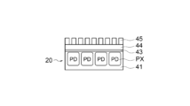
- Figures 41 to 48 are cross-sectional views illustrating an example of a manufacturing method for an image sensor 1 (particularly an image sensor 1 having a wire-grid type additional polarizer 11).
- a substrate 41 having a photodiode PD that constitutes a light-receiving pixel PX is prepared.
- the photodiode PD can be formed on the substrate 41 by any method.
- a photodiode PD can be formed for each pixel by doping a p-type Si substrate 41 by ion-implanting an n-type dopant, and activating the doped material by high-temperature annealing.
- an anti-reflection film (AR (Anti-Reflection) film) 43, a silicon dioxide film 44, and an aluminum film 45 are sequentially deposited and stacked on the substrate 41 so as to cover the photodiode PD.
- the anti-reflection film 43, the silicon dioxide film 44, and the aluminum film 45 can be stacked on the substrate 41 by any method (CVD (Chemical Vapor Deposition) is one example).
- the aluminum film 45 is processed to form an additional polarizer 11 as a wire grid type polarizer.
- the aluminum film 45 can be processed into a wire grid polarizer by any method.
- fine grooves through holes are formed in the aluminum film 45 by dry etching using a photoresist based on lithography technology (e.g., reactive ion etching (RIE)) (see Figure 43).
- RIE reactive ion etching
- a silicon dioxide film 46 is formed and laminated on the aluminum film 45 by any method (e.g., CVD), so that the fine grooves in the aluminum film 45 are filled with silicon dioxide (see Figure 44).
- an additional polarizer 11 is formed having wire lines 11a made of aluminum and inter-wire portions 11b made of silicon dioxide.
- the waveguide 30 is also formed by the silicon dioxide film 46 on the aluminum film 45.
- the polarization control unit 10 is formed on the silicon dioxide film 46 (waveguide 30).
- an amorphous silicon film 47 is formed and laminated on a silicon dioxide film 46 by any method (for example, CVD). Then, as shown in FIG. 46, a fine groove (through hole) is formed in the amorphous silicon film 47 by any method (for example, dry etching such as RIE). Then, as shown in FIG. 47, a silicon dioxide film 48 is formed and laminated on the amorphous silicon film 47 by any method (for example, CVD), so that the fine groove in the amorphous silicon film 47 is filled with silicon dioxide.
- CVD chemical etching
- a polarization control section 10 is formed with a metasurface structure having meta-atoms 10a made of amorphous silicon and a peripheral portion 10b of the structure made of silicon dioxide.
- holes are formed in the silicon dioxide film 48, the silicon dioxide filling the fine grooves of the amorphous silicon film 47 (structure peripheral portion 10b), and the silicon dioxide film 46.
- the holes can be formed by any method (e.g., dry etching such as RIE), and constitute the polarization control light shielding portion 31 (air layer).
- the image sensor 1 can be mass-produced.
- a polarization control unit 10 having a metasurface structure and a polarization splitter function is arranged as an upper layer of an additional polarizer 11 having a polarization filter function.
- the disclosed technology can be applied to various electronic devices and can be used in the general optoelectronics field (including fields related to image sensors).
- the image sensor 1 of each of the above-mentioned embodiments and modifications can be used as an imaging device included in a camera system.
- the image sensor 1 of each of the above-mentioned embodiments and modifications can also be applied to light detection devices other than imaging devices, making it possible to provide various electronic devices equipped with such light detection devices.
- Such electronic devices are capable of deriving the shape of a subject based on the detection results (including polarization information) of the light detection device (image sensor 1), and are particularly useful in situations where high sensitivity and extinction ratio are required, making it possible to detect the movement and shape of a subject with high accuracy and high speed.
- the optical detection device and electronic device disclosed herein are therefore capable of recognizing gestures made by humans based on the detection results (including polarization information), and can also be configured as a head-mounted display to detect the user's line of sight (eye movement, etc.).
- the optical detection device and electronic device disclosed herein can be applied, for example, to gaming applications, and can also be applied to VR (Virtual Reality) technology and AR (Augmented Reality) technology.
- optical detection device and electronic device disclosed herein are capable of high-speed detection of the subject shape based on the detection results (including polarization information), and therefore can be applied to cameras for industrial machinery, for example, manufacturing equipment such as product assembly systems using robots.
- the technical categories that embody the above-mentioned technical ideas are not limited.
- the above-mentioned technical ideas may be embodied by a computer program that causes a computer to execute one or more procedures (steps) included in a method of manufacturing or using the above-mentioned device.
- the above-mentioned technical ideas may also be embodied by a computer-readable non-transitory recording medium on which such a computer program is recorded.
- the present disclosure may also have the following configuration.
- a polarization control section that includes a plurality of microstructures that are two-dimensionally arranged and that selectively transmits a plurality of polarized lights in the incident light; an additional polarizer that receives the plurality of polarized lights from the polarization control unit and selectively transmits the plurality of polarized lights; a photoelectric conversion unit including a plurality of light receiving pixels that receive the plurality of polarized lights from the additional polarizer, The plurality of polarized lights transmitted through each of the polarization control unit and the additional polarizer include first polarized lights, second polarized lights, third polarized lights, and fourth polarized lights having different vibration directions from each other. Light detection device.
- the additional polarizer includes a wire grid polarizer. 3.
- the additional polarizer includes a photonic crystal polarizer. 3.
- the additional polarizer includes a plurality of additional polarization pixels and an additional polarization light shielding portion provided between adjacent additional polarization pixels; each of the plurality of additional polarization pixels selectively transmits any one of the first polarization, the second polarization, the third polarization, and the fourth polarization; 5.
- the optical detection device according to any one of items 1 to 4.
- the first polarized light and the second polarized light have vibration directions that are different by 90 degrees from each other, the third polarized light and the fourth polarized light have vibration directions that are different by 90 degrees from each other, The second polarized light and the third polarized light have vibration directions that differ by 45 degrees from each other.
- Item 6 A light detection device according to any one of items 1 to 5.
- the polarization control unit is a first unit polarization control section that selectively transmits the first polarized light and the second polarized light; a second unit polarization control section that selectively transmits the third polarized light and the fourth polarized light; Including, the additional polarizer includes a plurality of additional polarization pixels that selectively transmit any one of the first polarization, the second polarization, the third polarization, and the fourth polarization,
- the first unit polarization control section is Concentrating the first polarized light toward an additional polarization pixel that selectively transmits the first polarized light; Concentrating the second polarized light toward an additional polarization pixel that selectively transmits the second polarized light;
- the second unit polarization control section is Concentrating the third polarized light toward an additional polarization pixel that selectively transmits the third polarized light; Concentrating the fourth polarized light toward an additional polarization pixel that selectively transmits the fourth polarized light.
- a waveguide is provided between the polarization control section and the additional polarizer,
- the waveguide is a first unit polarization waveguide through which the first polarized light and the second polarized light output from the first unit polarization control section travel toward the additional polarizer;
- a second unit polarization waveguide through which the third polarized light and the fourth polarized light output from the second unit polarization control section travel toward the additional polarizer, a polarization control light shielding portion is provided between the first unit polarization waveguide and the second unit polarization waveguide adjacent to each other;
- Item 8 The optical detection device according to item 7.
- the polarization-control light shield includes a metal.
- Item 9 The optical detection device according to item 8.
- the polarization control light shielding portion includes an air layer.
- Item 9 The optical detection device according to item 8.
- the plurality of light receiving pixels have a diagonal lattice arrangement.
- the optical detection device according to any one of items 1 to 10.
- the additional polarizer includes a plurality of additional polarizing pixels having a diagonal lattice arrangement. Item 12. A light detection device according to any one of items 1 to 11.
- the polarization control unit includes a plurality of unit polarization control units having a diagonal lattice arrangement, Item 13.
- a light detection device according to any one of items 1 to 12.
- a polarization control section that includes a plurality of microstructures that are two-dimensionally arranged and that selectively transmits a plurality of polarized lights in the incident light; an additional polarizer that receives the plurality of polarized lights from the polarization control unit and selectively transmits the plurality of polarized lights; a photoelectric conversion unit including a plurality of light receiving pixels that receive the plurality of polarized lights from the additional polarizer; An electronic device comprising a photodetector, wherein the plurality of polarized lights passing through each of the polarization control unit and the additional polarizer include a first polarized light, a second polarized light, a third polarized light and a fourth polarized light having mutually different vibration directions.
- the additional polarizer includes a wire grid polarizer.
- Item 16 The electronic device according to item 14 or 15.
- the additional polarizer includes a photonic crystal polarizer.
- Item 16 The electronic device according to item 14 or 15.
- the additional polarizer includes a plurality of additional polarization pixels and an additional polarization light shielding portion provided between adjacent additional polarization pixels; each of the plurality of additional polarization pixels selectively transmits any one of the first polarization, the second polarization, the third polarization, and the fourth polarization; Item 18.
- An electronic device according to any one of items 14 to 17.
- the first polarized light and the second polarized light have vibration directions that are different by 90 degrees from each other, the third polarized light and the fourth polarized light have vibration directions that are different by 90 degrees from each other, The second polarized light and the third polarized light have vibration directions that differ by 45 degrees from each other.
- An electronic device according to any one of items 14 to 18.
- the polarization control unit is a first unit polarization control section that selectively transmits the first polarized light and the second polarized light; a second unit polarization control section that selectively transmits the third polarized light and the fourth polarized light; Including, the additional polarizer includes a plurality of additional polarization pixels that selectively transmit any one of the first polarization, the second polarization, the third polarization, and the fourth polarization,
- the first unit polarization control section is Concentrating the first polarized light toward an additional polarization pixel that selectively transmits the first polarized light; Concentrating the second polarized light toward an additional polarization pixel that selectively transmits the second polarized light;
- the second unit polarization control section is Concentrating the third polarized light toward an additional polarization pixel that selectively transmits the third polarized light; Concentrating the fourth polarized light toward an additional polarization pixel that selectively transmits the fourth polarized light.
- a waveguide is provided between the polarization control section and the additional polarizer,
- the waveguide is a first unit polarization waveguide through which the first polarized light and the second polarized light output from the first unit polarization control section travel toward the additional polarizer;
- a second unit polarization waveguide through which the third polarized light and the fourth polarized light output from the second unit polarization control section travel toward the additional polarizer, a polarization control light shielding portion is provided between the first unit polarization waveguide and the second unit polarization waveguide adjacent to each other;
- the polarization-control light shield includes a metal. 22. The electronic device according to item 21.
- the polarization control light shielding portion includes an air layer. 22. The electronic device according to item 21.
- the plurality of light receiving pixels have a diagonal lattice arrangement.
- Item 24 An electronic device according to any one of items 14 to 23.
- the additional polarizer includes a plurality of additional polarizing pixels having a diagonal lattice arrangement. Item 25. An electronic device according to any one of items 14 to 24.
- the polarization control unit includes a plurality of unit polarization control units having a diagonal lattice arrangement, Item 26.
- An electronic device according to any one of items 14 to 25.
Landscapes
- Physics & Mathematics (AREA)
- General Physics & Mathematics (AREA)
- Optics & Photonics (AREA)
- Solid State Image Pick-Up Elements (AREA)
- Polarising Elements (AREA)
Abstract
Le problème décrit par la présente invention est de fournir des techniques avantageuses pour limiter la réception de lumière d'une polarisation indésirable tout en obtenant une excellente sensibilité de réception de la lumière d'une polarisation souhaitée dans chaque pixel de réception de lumière. La solution selon l'invention porte sur un dispositif de détection de lumière qui comprend : une unité de commande de polarisation qui comprend un réseau bidimensionnel d'une pluralité de microstructures, et qui transmet sélectivement une pluralité de polarisations dans une lumière d'entrée ; un polariseur supplémentaire dans lequel pénètre une pluralité de polarisations provenant de l'unité de commande de polarisation et qui transmet sélectivement la pluralité de polarisations ; et une unité de conversion photoélectrique qui comprend une pluralité de pixels de réception de lumière pour recevoir la lumière d'une pluralité de polarisations provenant du polariseur supplémentaire. La pluralité de polarisations transmises par l'unité de commande de polarisation et le polariseur supplémentaire comprend une première polarisation, une deuxième polarisation, une troisième polarisation et une quatrième polarisation qui ont des directions d'oscillation mutuellement différentes.
Applications Claiming Priority (2)
| Application Number | Priority Date | Filing Date | Title |
|---|---|---|---|
| JP2023-014713 | 2023-02-02 | ||
| JP2023014713A JP2024110240A (ja) | 2023-02-02 | 2023-02-02 | 光検出装置及び電子機器 |
Publications (1)
| Publication Number | Publication Date |
|---|---|
| WO2024162000A1 true WO2024162000A1 (fr) | 2024-08-08 |
Family
ID=92146406
Family Applications (1)
| Application Number | Title | Priority Date | Filing Date |
|---|---|---|---|
| PCT/JP2024/001099 Ceased WO2024162000A1 (fr) | 2023-02-02 | 2024-01-17 | Dispositif de détection de lumière et appareil électronique |
Country Status (2)
| Country | Link |
|---|---|
| JP (1) | JP2024110240A (fr) |
| WO (1) | WO2024162000A1 (fr) |
Cited By (1)
| Publication number | Priority date | Publication date | Assignee | Title |
|---|---|---|---|---|
| WO2026048314A1 (fr) * | 2024-08-30 | 2026-03-05 | ソニーセミコンダクタソリューションズ株式会社 | Élément optique, dispositif de photodétection et appareil électronique |
Citations (6)
| Publication number | Priority date | Publication date | Assignee | Title |
|---|---|---|---|---|
| JP2010050702A (ja) * | 2008-08-21 | 2010-03-04 | Fujifilm Corp | 撮像装置 |
| WO2017169968A1 (fr) * | 2016-03-30 | 2017-10-05 | 富士フイルム株式会社 | Film optique stratifié et capteur d'imagerie de polarisation |
| CN108007575A (zh) * | 2017-11-29 | 2018-05-08 | 中国科学院光电技术研究所 | 一种基于二元数字编码双折射晶体的小型化全斯托克斯矢量偏振成像装置 |
| JP2018182022A (ja) * | 2017-04-11 | 2018-11-15 | ソニーセミコンダクタソリューションズ株式会社 | 固体撮像装置 |
| JP2020051868A (ja) * | 2018-09-26 | 2020-04-02 | 日本電信電話株式会社 | 偏光イメージング撮像システム |
| WO2021234924A1 (fr) * | 2020-05-21 | 2021-11-25 | 日本電信電話株式会社 | Élément de capture d'image et dispositif de capture d'image |
-
2023
- 2023-02-02 JP JP2023014713A patent/JP2024110240A/ja active Pending
-
2024
- 2024-01-17 WO PCT/JP2024/001099 patent/WO2024162000A1/fr not_active Ceased
Patent Citations (6)
| Publication number | Priority date | Publication date | Assignee | Title |
|---|---|---|---|---|
| JP2010050702A (ja) * | 2008-08-21 | 2010-03-04 | Fujifilm Corp | 撮像装置 |
| WO2017169968A1 (fr) * | 2016-03-30 | 2017-10-05 | 富士フイルム株式会社 | Film optique stratifié et capteur d'imagerie de polarisation |
| JP2018182022A (ja) * | 2017-04-11 | 2018-11-15 | ソニーセミコンダクタソリューションズ株式会社 | 固体撮像装置 |
| CN108007575A (zh) * | 2017-11-29 | 2018-05-08 | 中国科学院光电技术研究所 | 一种基于二元数字编码双折射晶体的小型化全斯托克斯矢量偏振成像装置 |
| JP2020051868A (ja) * | 2018-09-26 | 2020-04-02 | 日本電信電話株式会社 | 偏光イメージング撮像システム |
| WO2021234924A1 (fr) * | 2020-05-21 | 2021-11-25 | 日本電信電話株式会社 | Élément de capture d'image et dispositif de capture d'image |
Cited By (1)
| Publication number | Priority date | Publication date | Assignee | Title |
|---|---|---|---|---|
| WO2026048314A1 (fr) * | 2024-08-30 | 2026-03-05 | ソニーセミコンダクタソリューションズ株式会社 | Élément optique, dispositif de photodétection et appareil électronique |
Also Published As
| Publication number | Publication date |
|---|---|
| JP2024110240A (ja) | 2024-08-15 |
Similar Documents
| Publication | Publication Date | Title |
|---|---|---|
| US11733100B2 (en) | Polarization imaging system | |
| US9590004B2 (en) | Solid-state imaging device and imaging apparatus | |
| KR102201627B1 (ko) | 고체 촬상 소자 및 촬상 장치 | |
| EP2432019B1 (fr) | Dispositif d'imagerie et appareil d'imagerie | |
| KR102772647B1 (ko) | 편광 스크램블링을 위한 광 가이드 광학 요소 | |
| CN105280655B (zh) | 光电转换装置与成像系统 | |
| JP7364066B2 (ja) | 撮像素子及び撮像装置 | |
| US20110074960A1 (en) | Solid state imaging device | |
| WO2019202890A1 (fr) | Élément de capture d'image couleur et dispositif de capture d'image | |
| EP3338305B1 (fr) | Système et procédé d'extension de la réponse spectrale dans le proche infrarouge pour systèmes d'imagerie | |
| KR102832511B1 (ko) | 분광소자 어레이, 촬상소자 및 촬상장치 | |
| JP6981496B2 (ja) | カラー撮像素子および撮像装置 | |
| US9565381B2 (en) | Solid-state image sensor and image-capturing device | |
| US20160071895A1 (en) | Image sensor and electronic device including the same | |
| WO2024162000A1 (fr) | Dispositif de détection de lumière et appareil électronique | |
| US20240201016A1 (en) | Polarizing filter and polarimetric image sensor integrating such a filter | |
| US20210263219A1 (en) | Planar Lightwave Circuit and Optical Device | |
| US20170077154A1 (en) | Image sensor and image pickup apparatus including the same | |
| US12584795B2 (en) | Polarimetric image sensor | |
| CN218824769U (zh) | 光学模组及光学设备 | |
| JP7563471B2 (ja) | 撮像素子及び撮像装置 | |
| KR20230154741A (ko) | 색분리 메타 구조를 포함하는 이미지 센서와 이러한 이미지 센서를 포함하는 전자장치 | |
| JP2025016280A (ja) | 光検出装置 | |
| Maekawa et al. | Proposal of single-layer full-color AR glasses with two-dimensional mesh diffraction gratings | |
| US20250362522A1 (en) | Photodetection device |
Legal Events
| Date | Code | Title | Description |
|---|---|---|---|
| 121 | Ep: the epo has been informed by wipo that ep was designated in this application |
Ref document number: 24749954 Country of ref document: EP Kind code of ref document: A1 |
|
| NENP | Non-entry into the national phase |
Ref country code: DE |
|
| 122 | Ep: pct application non-entry in european phase |
Ref document number: 24749954 Country of ref document: EP Kind code of ref document: A1 |