WO2024190845A1 - 伝送回路 - Google Patents
伝送回路 Download PDFInfo
- Publication number
- WO2024190845A1 WO2024190845A1 PCT/JP2024/009897 JP2024009897W WO2024190845A1 WO 2024190845 A1 WO2024190845 A1 WO 2024190845A1 JP 2024009897 W JP2024009897 W JP 2024009897W WO 2024190845 A1 WO2024190845 A1 WO 2024190845A1
- Authority
- WO
- WIPO (PCT)
- Prior art keywords
- signal
- circuit
- impedance
- frequency
- electrically connected
- Prior art date
- Legal status (The legal status is an assumption and is not a legal conclusion. Google has not performed a legal analysis and makes no representation as to the accuracy of the status listed.)
- Ceased
Links
Images









Classifications
-
- H—ELECTRICITY
- H04—ELECTRIC COMMUNICATION TECHNIQUE
- H04B—TRANSMISSION
- H04B1/00—Details of transmission systems, not covered by a single one of groups H04B3/00 - H04B13/00; Details of transmission systems not characterised by the medium used for transmission
- H04B1/59—Responders; Transponders
Definitions
- This disclosure relates to a transmission circuit.
- Patent Document 1 discloses a technology that uses a splitter/combiner to suppress either the USB (Upper Side Band) signal or the LSB (Lower Side Band) signal to achieve a single sideband.
- the transmission circuit of the present disclosure includes an impedance rotation circuit having an impedance circuit configured to be connected to an antenna and a control circuit that controls the reflection coefficient of the impedance rotation circuit to rotate the reflection coefficient in a complex plane, and the control circuit changes the modulation speed of the reflected signal of the impedance rotation circuit depending on the communication environment.
- FIG. 1 is a diagram illustrating an example of the configuration of a communication system according to the first embodiment.
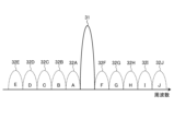
- FIG. 2 is a diagram showing the signal levels of a transmission signal and a reflected signal in an ideal environment according to the first embodiment.
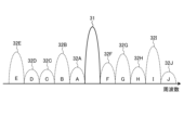
- FIG. 3 is a diagram showing the signal levels of a transmission signal and a reflected signal in an actual environment according to the first embodiment.
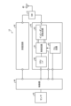
- FIG. 4 is a block diagram showing an example of the configuration of the slave unit according to the first embodiment.
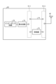
- FIG. 5 is a diagram showing an example of the configuration of the impedance rotation circuit according to the first embodiment.
- FIG. 6 is a diagram illustrating an example of the configuration of the impedance circuit according to the first embodiment.
- FIG. 7 is a diagram illustrating an example of the configuration of a matching circuit according to the first embodiment.
- FIG. 1 is a diagram illustrating an example of the configuration of a communication system according to the first embodiment.
- FIG. 2 is a diagram showing the signal levels of a transmission signal and a reflected signal in
- FIG. 8 is a diagram showing signal waveforms in normal backscatter communication according to the first embodiment.
- FIG. 9 is a diagram showing signal waveforms in backscatter communication according to the first example of the first embodiment.
- FIG. 10 is a diagram showing signal waveforms of subcarrier signals according to the first example of the first embodiment.
- FIG. 11 is a diagram for explaining a method of controlling the modulation rate according to the first embodiment.
- FIG. 12 is a diagram showing signal waveforms in backscatter communication according to the second example of the first embodiment.
- FIG. 13 is a diagram showing signal waveforms of subcarrier signals according to the second example of the first embodiment.
- FIG. 14 is a diagram showing signal waveforms in backscatter communication according to the third example of the first embodiment.
- FIG. 15 is a diagram showing signal waveforms of subcarrier signals according to the third example of the first embodiment.
- FIG. 16 is a diagram showing the relationship between the frequency of the subcarrier signal, the symbol rate, and the number of rotations of the symbol point according to the first embodiment.
- FIG. 17 is a diagram showing the relationship between the frequency of the oscillation signal and the frequency of the subcarrier signal according to the second embodiment.
- FIG. 18 is a diagram showing the relationship between the frequency of the oscillation signal, the frequency of the subcarrier signal, and the number of symbol points according to the third embodiment.
- FIG. 19 is a diagram illustrating an example of the configuration of an impedance rotation circuit according to the fourth embodiment.
- FIG. 20 is a diagram for explaining a modulation scheme according to a first example of the fourth embodiment.
- FIG. 21 is a diagram for explaining a modulation scheme according to a second example of the fourth embodiment.
- FIG. 22 is a diagram for explaining a modulation scheme according to a third example of the fourth embodiment.
- FIG. 23 is a diagram for explaining a modulation scheme according to a fourth example of the fourth embodiment.
- FIG. 24 is a diagram for explaining a modulation scheme according to a fifth example of the fourth embodiment.
- FIG. 25 is a diagram for explaining a modulation scheme according to a sixth example of the fourth embodiment.
- FIG. 1 is a diagram showing a configuration example of a communication system according to the first embodiment.
- communication system 1 includes parent unit 10, child unit 12A, child unit 12B, child unit 12C, child unit 12D, child unit 12E, child unit 12F, child unit 12G, child unit 12H, child unit 12I, and child unit 12J.
- Child unit 12A When there is no need to distinguish child unit 12A from child unit 12J, they are collectively referred to as child unit 12.
- Communication system 1 is a system that performs data communication using a backscatter method.
- Parent unit 10 and child unit 12 are wireless communication devices that perform backscatter communication.
- child unit 12 is configured to transmit to parent unit 10 a reflected signal 22 that reflects a transmission signal 21 transmitted by the parent unit.
- (signal level) 2 is a diagram showing the signal levels of a transmission signal and a reflected signal in an ideal environment according to the first embodiment.
- Waveform 31 shows the signal level of the transmission signal 21 transmitted by the parent unit.
- Waveforms 32A to 32J show the signal levels of the reflected signals 22 reflected by the child units 12A to 12J, respectively.
- the signal levels of the reflected signals 22 reflected by the child units 12A to 12J are ideally the same. In an ideal environment, each of the child units 12A to 12J can properly communicate with the parent unit 10 without being disturbed by the reflected signals 22 reflected by the other child units 12.
- FIG. 3 is a diagram showing the signal levels of the transmission signal and the reflected signal in the first embodiment in a real environment.
- the signal levels of the reflected signal 22 reflected by each of the slave units 12A and 12J may differ.
- the slave unit 12J is assigned to a communication channel that the slave unit 12E has suppressed by making it a single sideband.
- the reflected signal 22 of the slave unit 12E may become an interference signal that makes it difficult for the slave unit 12J to communicate with the master unit 10. In such a case, it is required to appropriately suppress the signal level of the reflected signal 22 of the slave unit 12E.
- Fig. 4 is a block diagram showing an example of the configuration of the slave unit according to the first embodiment.
- the handset 12 includes an antenna 40, a switch (SW) 41, a receiving circuit 42, a transmitting circuit 43, a control unit 44, and a sensor 45.
- SW switch
- the antenna 40 is configured to receive a transmission signal transmitted by the parent unit 10.
- the antenna 40 is configured to transmit a reflected signal that reflects the transmission signal to the parent unit 10.
- the switch 41 is configured to be able to switch the path between the antenna 40 and the receiving circuit 42 and the transmitting circuit 43.
- the switch 41 electrically connects the antenna 40 to the receiving circuit 42.
- the switch 41 electrically connects the antenna 40 to the transmitting circuit 43.
- the receiving circuit 42 receives the transmission signal from the parent unit 10 received by the antenna 40.
- the receiving circuit 42 is configured to perform various reception processes on the transmission signal.
- the transmission circuit 43 is a circuit that generates a reflected signal (also called a backscatter signal) transmitted by the antenna 40.
- the transmission circuit 43 includes a CPU interface (I/F) 60, a control circuit 61, an impedance rotation circuit 62, and a PLL (Phase Looked Loop) circuit 63.
- the CPU interface 60 is configured to receive various control signals and data from the control unit 44.
- the control circuit 61 is configured to control the impedance rotation circuit 62.
- the control circuit 61 controls the impedance rotation circuit 62 based on a control signal input from the control unit 44 via the CPU interface 60, an oscillation signal input from the PLL circuit 63, and the like.
- the control circuit 61 is configured to change the impedance of the impedance rotation circuit 62.
- the control circuit 61 changes the impedance of the impedance rotation circuit 62 to control the reflection coefficient of the output terminal on the antenna 40 side to rotate in the complex plane.
- the control circuit 61 for example, reduces the USB (Upper Side Band) signal or LSB (Lower Side Band) signal for the carrier signal of the backscatter signal to realize a single sideband.
- the impedance rotation circuit 62 is disposed at the front end of the child device 12.
- the impedance rotation circuit 62 is configured to reflect the transmission signal sent by the child device 12 as a backscatter signal and perform backscatter communication.
- the impedance rotation circuit 62 includes multiple impedance circuits, each of which has a different impedance.
- the control circuit 61 and the impedance rotation circuit 62 are a type of transmission circuit of the present disclosure.
- the PLL circuit 63 is configured to generate an oscillation signal of a predetermined frequency.
- the PLL circuit 63 generates the oscillation signal in accordance with a control signal from the control unit 44.
- the PLL circuit 63 is configured to output the generated oscillation signal to the control circuit 61.
- the control unit 44 is configured to control each part of the handset 12.
- the control unit 44 may be realized, for example, by an information processing device such as a CPU (Central Processing Unit) or an MPU (Micro Processing Unit), and a storage device such as a RAM (Random Access Memory) or a ROM (Read Only Memory).
- the control unit 44 may be realized, for example, by an integrated circuit such as an ASIC (Application Specific Integrated Circuit) or an FPGA (Field Programmable Gate Array).
- the control unit 44 may be realized by a combination of hardware and software.
- the sensor 45 includes various sensors.
- the sensor 45 may include, for example, a speed sensor, a vibration sensor, an acceleration sensor, a gyro sensor, a rotation angle sensor, an angular velocity sensor, a geomagnetic sensor, a magnet sensor, a temperature sensor, a humidity sensor, an air pressure sensor, a light sensor, an illuminance sensor, a UV sensor, a gas sensor, a gas concentration sensor, an atmosphere sensor, a level sensor, an odor sensor, a pressure sensor, an air pressure sensor, a contact sensor, a wind sensor, an infrared sensor, a human presence sensor, a displacement sensor, an image sensor, a weight sensor, a smoke sensor, a leakage sensor, a vital sensor, a battery remaining amount sensor, and an ultrasonic sensor.
- the sensor 45 may include a GNSS (Global Navigation Satellite System) sensor that acquires the current location information of the handset 12.
- GNSS Global Navigation Satellite System
- Fig. 5 is a diagram showing a configuration example of the impedance rotation circuit according to the first embodiment.
- the impedance rotation circuit 62 includes an impedance circuit 70, a switch 72-1, a switch 72-2, a matching circuit 73, wiring 74, and a phase shifter 75.
- the output terminal of the impedance circuit 70 is electrically connected to the input terminal of the matching circuit 73.
- the impedance circuit 70 adds impedance to the impedance rotation circuit 62.
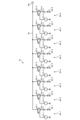
- FIG. 6 is a diagram showing an example of the configuration of the impedance circuit according to the first embodiment.
- the impedance circuit 70 includes a first circuit 80-1, a second circuit 80-2, a third circuit 80-3, a fourth circuit 80-4, a fifth circuit 80-5, a sixth circuit 80-6, a seventh circuit 80-7, and an eighth circuit 80-8.
- the first circuit 80-1 to the eighth circuit 80-8 are electrically connected by a signal line 85.
- the output terminal 70a of the impedance circuit 70 is electrically connected to the input terminal of the matching circuit 73.
- the first circuit 80-1 includes a signal source 81-1, a switch element 82-1, a resistor element 83-1, and a capacitor 84-1.
- the signal source 81-1 indicates a signal source of a control signal from the control circuit 61 for controlling the switch element 82-1.
- One end of the signal source 81-1 is electrically connected to a reference potential.
- the reference potential is, for example, but is not limited to, ground.
- the signal source 81-1 outputs a control signal for controlling the on and off states of the switch element 82-1 to the switch element 82-1.
- One end of the switch element 82-1 is electrically connected to a signal line 85.
- One end of the switch element 82-1 is electrically connected to one end of the resistor element 83-1.
- the other end of the resistor element 83-1 is electrically connected to one end of the capacitor 84-1.
- the other end of the capacitor 84-1 is electrically connected to the reference potential.
- the switch element 82-1 When the switch element 82-1 is turned on, the resistor element 83-1 and the capacitor 84-1 are electrically connected to the signal line 85.
- the impedance of the impedance circuit 70 changes according to the resistance value of the resistor element 83-1 and the capacitance value of the capacitor 84-1.
- the second circuit 80-2 includes a signal source 81-2, a switch element 82-2, a resistive element 83-2, and a capacitor 84-2.
- the signal source 81-2 indicates a signal source of a control signal from the control circuit 61 for controlling the switch element 82-2. One end of the signal source 81-2 is electrically connected to a reference potential. The signal source 81-2 outputs a control signal for controlling the on state and off state of the switch element 82-2 to the switch element 82-2. One end of the switch element 82-2 is electrically connected to a signal line 85. One end of the switch element 82-2 is electrically connected to one end of the resistive element 83-2. The other end of the resistive element 83-2 is electrically connected to one end of the capacitor 84-2.
- the other end of the capacitor 84-2 is electrically connected to the reference potential.
- the switch element 82-2 When the switch element 82-2 is in the on state, the resistive element 83-2 and the capacitor 84-2 are electrically connected to the signal line 85.
- the impedance of the impedance circuit 70 changes depending on the resistance value of the resistive element 83-2 and the capacitance value of the capacitor 84-2.
- the third circuit 80-3 includes a signal source 81-3, a switch element 82-3, a resistor element 83-3, and a capacitor 84-3.
- the signal source 81-3 indicates a signal source of a control signal from the control circuit 61 for controlling the switch element 82-3.
- One end of the signal source 81-3 is electrically connected to a reference potential.
- the signal source 81-3 outputs a control signal for controlling the on state and off state of the switch element 82-3 to the switch element 82-3.
- One end of the switch element 82-3 is electrically connected to a signal line 85.
- One end of the switch element 82-3 is electrically connected to one end of the resistor element 83-3.
- the other end of the resistor element 83-3 is electrically connected to one end of the capacitor 84-3.
- the other end of the capacitor 84-3 is electrically connected to the reference potential.
- the switch element 82-3 When the switch element 82-3 is in the on state, the resistor element 83-3 and the capacitor 84-3 are electrically connected to the signal line 85.
- the impedance of the impedance circuit 70 changes depending on the resistance value of the resistive element 83-3 and the capacitance value of the capacitor 84-3.
- the fourth circuit 80-4 includes a signal source 81-4, a switch element 82-4, a resistor element 83-4, and a capacitor 84-4.
- the signal source 81-4 indicates a signal source of a control signal from the control circuit 61 for controlling the switch element 82-4.
- One end of the signal source 81-4 is electrically connected to a reference potential.
- the signal source 81-4 outputs a control signal for controlling the on state and off state of the switch element 82-4 to the switch element 82-4.
- One end of the switch element 82-4 is electrically connected to a signal line 85.
- One end of the switch element 82-4 is electrically connected to one end of the resistor element 83-4.
- the other end of the resistor element 83-4 is electrically connected to one end of the capacitor 84-4.
- the other end of the capacitor 84-4 is electrically connected to the reference potential.
- the switch element 82-4 When the switch element 82-4 is in the on state, the resistor element 83-4 and the capacitor 84-4 are electrically connected to the signal line 85.
- the impedance of the impedance circuit 70 changes depending on the resistance value of the resistive element 83-4 and the capacitance value of the capacitor 84-4.
- the fifth circuit 80-5 includes a signal source 81-5, a switch element 82-5, a resistive element 83-5, and a capacitor 84-5.
- the signal source 81-5 indicates a signal source of a control signal from the control circuit 61 for controlling the switch element 82-5.
- One end of the signal source 81-5 is electrically connected to a reference potential.
- the signal source 81-5 outputs a control signal for controlling the on state and off state of the switch element 82-5 to the switch element 82-5.
- One end of the switch element 82-5 is electrically connected to a signal line 85.
- One end of the switch element 82-5 is electrically connected to one end of the resistive element 83-5.
- the other end of the resistive element 83-5 is electrically connected to one end of the capacitor 84-5.
- the other end of the capacitor 84-5 is electrically connected to the reference potential.
- the switch element 82-5 When the switch element 82-5 is in the on state, the resistive element 83-5 and the capacitor 84-5 are electrically connected to the signal line 85.
- the impedance of the impedance circuit 70 changes depending on the resistance value of the resistor element 83-5 and the capacitance value of the capacitor 84-5.
- the sixth circuit 80-6 includes a signal source 81-6, a switch element 82-6, a resistor element 83-6, and a capacitor 84-6.
- the signal source 81-6 indicates a signal source of a control signal from the control circuit 61 for controlling the switch element 82-6.
- One end of the signal source 81-6 is electrically connected to a reference potential.
- the signal source 81-6 outputs a control signal for controlling the on state and off state of the switch element 82-6 to the switch element 82-6.
- One end of the switch element 82-6 is electrically connected to a signal line 85.
- One end of the switch element 82-6 is electrically connected to one end of the resistor element 83-6.
- the other end of the resistor element 83-6 is electrically connected to one end of the capacitor 84-6.
- the other end of the capacitor 84-6 is electrically connected to the reference potential.
- the switch element 82-6 When the switch element 82-6 is in the on state, the resistor element 83-6 and the capacitor 84-6 are electrically connected to the signal line 85.
- the impedance of the impedance circuit 70 changes depending on the resistance value of the resistor element 83-6 and the capacitance value of the capacitor 84-6.
- the seventh circuit 80-7 includes a signal source 81-7, a switch element 82-7, a resistor element 83-7, and a capacitor 84-7.
- the signal source 81-7 indicates a signal source of a control signal from the control circuit 61 for controlling the switch element 82-7.
- One end of the signal source 81-7 is electrically connected to a reference potential.
- the signal source 81-7 outputs a control signal for controlling the on state and off state of the switch element 82-7 to the switch element 82-7.
- One end of the switch element 82-7 is electrically connected to a signal line 85.
- One end of the switch element 82-7 is electrically connected to one end of the resistor element 83-7.
- the other end of the resistor element 83-7 is electrically connected to one end of the capacitor 84-7.
- the other end of the capacitor 84-7 is electrically connected to the reference potential.
- the switch element 82-7 is in the on state, the resistor element 83-7 and the capacitor 84-7 are electrically connected to the signal line 85.
- the impedance of the impedance circuit 70 changes depending on the resistance value of the resistor element 83-7 and the capacitance value of the capacitor 84-7.
- the eighth circuit 80-8 includes a signal source 81-8, a switch element 82-8, a resistor element 83-8, and a capacitor 84-8.
- the signal source 81-8 indicates a signal source of a control signal from the control circuit 61 for controlling the switch element 82-8.
- One end of the signal source 81-8 is electrically connected to a reference potential.
- the signal source 81-8 outputs a control signal for controlling the on state and off state of the switch element 82-8 to the switch element 82-8.
- One end of the switch element 82-8 is electrically connected to a signal line 85.
- One end of the switch element 82-8 is electrically connected to one end of the resistor element 83-8.
- the other end of the resistor element 83-8 is electrically connected to one end of the capacitor 84-8.
- the other end of the capacitor 84-8 is electrically connected to the reference potential.
- the switch element 82-8 is in the on state, the resistor element 83-8 and the capacitor 84-8 are electrically connected to the signal line 85.
- the impedance of the impedance circuit 70 changes depending on the resistance value of the resistor element 83-8 and the capacitance value of the capacitor 84-8.
- the control circuit 61 is configured to selectively change the impedance rotation circuit and rotate the reflection coefficient on the polar chart by selectively controlling the on and off states of each of the switch elements 82-1 to 82-8.
- the matching circuit 73 is a circuit that matches the output impedance of the impedance circuit 70 with the input impedance of the antenna 40.
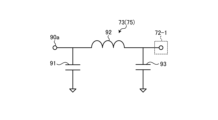
- FIG. 7 is a diagram showing an example of the configuration of a matching circuit according to the first embodiment.
- the matching circuit 73 includes a capacitor 91, an inductor 92, and a capacitor 93.
- One end of the capacitor 91 is electrically connected to the input terminal 90a of the matching circuit 73 and one end of the inductor 92.
- the other end of the capacitor 91 is electrically connected to a reference potential.
- One end of the capacitor 93 is electrically connected to the switch 72-1 and the other end of the inductor 92.
- the other end of the capacitor 93 is electrically connected to the reference potential.
- the matching circuit 73 is selectively connected to the wiring 74 or the phase shifter 75 by the switch 72-1.
- the switch 72-1 is, for example, a transistor, but is not limited to this.
- the switch 72-1 is controlled by the control circuit 61.
- the wiring 74 or the phase shifter 75 is selectively connected to the input terminal of the antenna 40 by the switch 72-2.
- the switch 72-2 is controlled by the control circuit 61.
- the phase shifter 75 has the same configuration as the matching circuit 73 shown in FIG. 7, so a description thereof is omitted.
- the phase shifter 75 shifts the phase of the input signal by 90° and outputs it.
- the signal output from the matching circuit 73 is input to the input terminal of the antenna 40 without any change in phase.
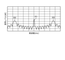
- Fig. 8 is a diagram showing a signal waveform in backscatter communication during normal backscatter communication according to the first embodiment.
- carrier signal 201 indicates the signal level of the transmission signal from parent device 10
- subcarrier signal 202 and subcarrier signal 203 indicate the signal level of the subcarrier signal (reflected signal) from the same child device 12.
- the frequency of subcarrier signal 202 is -800 [kHz].
- the frequency of subcarrier signal 203 is +800 [kHz].
- the symbol rate of subcarrier signal 202 and subcarrier signal 203 is 100 [kHz]. The symbol rate is also called the modulation speed.
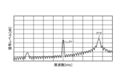
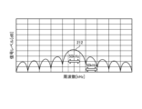
- FIG. 9 is a diagram showing a signal waveform in backscatter communication according to the first example of the first embodiment.
- FIG. 10 is a diagram showing a signal waveform of a subcarrier signal according to the first example of the first embodiment.
- a carrier signal 211 indicates a signal level of a transmission signal from the parent device 10
- a subcarrier signal 212 indicates a signal level of a subcarrier signal from the child device 12.
- the frequency of the subcarrier signal 212 is +800 [kHz].
- the symbol rate of the subcarrier signal 212 is 50 [kHz]. That is, in the example shown in FIG. 9, the symbol rate of the subcarrier signal is changed from 100 [kHz] to 50 [kHz] compared to normal times.
- the control circuit 61 changes the symbol rate by controlling the impedance rotation circuit 62.
- FIG. 11 is a diagram for explaining a method of controlling the modulation rate according to the first embodiment.
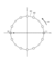
- FIG. 11 shows an IQ plane.
- the IQ plane is a complex plane with the horizontal axis (real axis) as the in-phase axis (I axis) and the vertical axis (imaginary axis) as the quadrature axis (Q axis).
- symbol points 302 are arranged on a circle 301.
- the symbol points 302 rotate so as to move among the positions of 16 points arranged at equal intervals on the circle 301.
- the control circuit 61 moves the position of the symbol point 302 at a timing when the symbol point 302 has rotated a predetermined number of times in accordance with the frequency and symbol rate of the subcarrier signal 212.
- Fig. 12 is a diagram showing a signal waveform in backscatter communication according to the second example of the first embodiment.
- Fig. 13 is a diagram showing a signal waveform of a subcarrier signal according to the second example of the first embodiment.
- a carrier signal 221 indicates the signal level of a transmission signal from the parent device 10
- a subcarrier signal 222 indicates the signal level of a subcarrier signal from the child device 12.
- the frequency of the subcarrier signal 222 is +800 [kHz].
- the symbol rate of the subcarrier signal 222 is 100 [kHz].
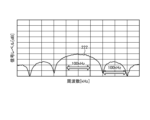
- Fig. 14 is a diagram showing a signal waveform in backscatter communication according to the third example of the first embodiment.
- Fig. 15 is a diagram showing a signal waveform of a subcarrier signal according to the third example of the first embodiment.
- a carrier signal 231 indicates the signal level of a transmission signal from the parent device 10
- a subcarrier signal 232 indicates the signal level of a subcarrier signal from the child device 12.
- the frequency of the subcarrier signal 232 is +800 [kHz].
- the symbol rate of the subcarrier signal 232 is 200 [kHz].
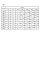
- FIG. 16 is a diagram showing the relationship between the frequency of the subcarrier signal, the symbol rate, and the number of rotations of the symbol point according to the first embodiment.
- fs [kHz] indicates the symbol rate
- fc [kHz] indicates the frequency of the subcarrier signal.
- the symbol rate is 25 [kHz] and the frequency of the subcarrier signal is 100 [kHz]
- the data position is moved at the timing of four rotations of the symbol point.
- the symbol rate is 50 [kHz] and the frequency of the subcarrier signal is 100 [kHz]
- the data position is moved at the timing of two rotations of the symbol point.
- the symbol rate is 100 [kHz] and the frequency of the subcarrier signal is 100 [kHz]
- the data position is moved at the timing of one rotation of the symbol point.
- the timing for moving the data position can be determined by the number of rotations according to the frequency and symbol rate of the subcarrier signal. This allows the first embodiment to perform backscatter communication at an appropriate symbol rate according to the communication environment.
- control circuit 61 calculates the frequency of the subcarrier signal based on the oscillation signal received from the PLL circuit 63.
- the frequency of the subcarrier signal is calculated by the following equation (2).
- Subcarrier signal frequency oscillation signal frequency / symbol number (2)
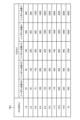
- FIG. 17 is a diagram showing the relationship between the frequency of the oscillation signal and the frequency of the subcarrier signal according to the second embodiment.
- Table TB2 shown in FIG. 17 shows the relationship between the frequency of the oscillation signal and the frequency of the subcarrier signal when the number of symbol points is 16.
- CLK [MHz] indicates the frequency of the oscillation signal
- fc [kHz] indicates the frequency of the subcarrier signal.
- the frequency of the oscillation signal is 1.6 [MHz]
- the frequency of the subcarrier signal is 100 [kHz].
- the frequency of the subcarrier signal is 1000 [kHz].
- the second embodiment can appropriately set the frequency of the subcarrier signal based on the oscillation signal of the PLL circuit 63.
- a subcarrier signal having a desired frequency is generated by calculating the frequency of the subcarrier signal using an oscillation signal and controlling the number of symbol points.
- FIG. 18 is a diagram showing the relationship between the frequency of the oscillation signal, the frequency of the subcarrier signal, and the number of symbol points according to the third embodiment.
- CLK [MHz] indicates the frequency of the oscillation signal
- fc [kHz] indicates the frequency of the subcarrier signal.
- the control circuit 61 can set the frequency of the subcarrier signal to 25 [kHz].
- the control circuit 61 can set the frequency of the subcarrier signal to 50 [kHz].
- the control circuit 61 can set the frequency of the subcarrier signal to 100 [kHz]. For example, when the frequency of the oscillation signal is 1.6 [MHz] and the number of symbol points is 8, the control circuit 61 can set the frequency of the subcarrier signal to 200 [kHz]. For example, when the frequency of the oscillation signal is 1.6 MHz and the number of symbols is four, the control circuit 61 can set the frequency of the subcarrier signal to 400 kHz.
- the frequency of the subcarrier signal can be set more appropriately based on the oscillation signal of the PLL circuit 63.
- the symbol rate can be changed by changing the modulation method.
- the impedance rotation circuit 62 has only one impedance circuit, and therefore uses symbol points on the same amplitude.
- modulation methods such as BPSK (Binary Phase Shift Keying), QPSK (Quadrature Phase Shift Keying), 8PSK (8 Phase Shift Keying), and 16PSK (16 Phase Shift Keying) can be supported.
- QAM Quadratture Amplitude Modulation
- multiple impedance circuits with different reflection coefficients are added to make it possible to support QAM modulation.
- Fig. 19 is a diagram showing a configuration example of the impedance rotation circuit according to the fourth embodiment.
- the impedance rotation circuit 62A includes impedance circuits 70-1 to 70-n (n is an integer equal to or greater than 2), switches 72-1, 72-2, and 72-3, a matching circuit 73, wiring 74, and a phase shifter 75. Different reflection coefficients are set for the impedance circuits 70-1 to 70-n. When there is no need to distinguish between the impedance circuits 70-1 to 70-n, they are collectively referred to as impedance circuits 70. In other words, the impedance rotation circuit 62A includes multiple impedance circuits 70 with different reflection coefficients.
- the impedance circuits 70-1 to 70-n are electrically connected to the matching circuit 73 by the switch 72-1.
- the switch 72-1 is, for example, but not limited to, a transistor.
- the switch 72-1 is controlled by the control circuit 61.
- the switch 72-1 is configured to selectively connect any one of the impedance circuits 70-1 to 70-n to the matching circuit 73.
- the control circuit 61 can control the reflection coefficient by controlling the switch 72-1 to switch the impedance circuit 70 to be connected. For example, but not limited to, a different reflection coefficient can be set in increments of 0.1 for each of the impedance circuits 70-1 to 70-n.
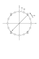
- FIG. 20 is a diagram for explaining a modulation scheme according to a first example of the fourth embodiment.
- FIG. 20 shows an IQ plane.
- the modulation scheme according to the first example of the fourth embodiment is BPSK.
- the number of symbol points 302 is 16.
- the symbol point 302 can be located at a position of [1] or [0] on the IQ plane.
- the control circuit 61 moves the symbol point 302 from the position of [1] to the position of [0] at the timing when the symbol point 302 rotates 16 points a predetermined number of times.
- FIG. 21 is a diagram for explaining a modulation method according to a second example of the fourth embodiment.
- FIG. 20 shows an IQ plane.
- the modulation method according to the second example of the fourth embodiment is QPSK.
- the number of symbol points 302 is 16.
- the symbol points 302 can be located at positions [11], [10], [00], or [01] on the IQ plane.
- the control circuit 61 moves the symbol points 302 from the position [11] to the position [00] at the timing when the symbol points 302 rotate a predetermined number of times through 16 points.
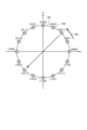
- FIG. 22 is a diagram for explaining a modulation method according to a third example of the fourth embodiment.
- FIG. 22 shows an IQ plane.
- the modulation method according to the third example of the fourth embodiment is 8PSK.
- the number of symbol points 302 is 16.
- the symbol point 302 can be located at a position of [000], [001], [011], [010], [100], [101], [111], or [110] on the IQ plane.
- the control circuit 61 moves the symbol point 302 from the position of [001] to the position of [101] at a timing when the symbol point 302 rotates 16 points a predetermined number of times.
- FIG. 23 is a diagram for explaining a modulation method according to a fourth example of the fourth embodiment.
- FIG. 23 shows an IQ plane.
- the modulation method according to the fourth example of the fourth embodiment is 16PSK.
- the number of symbol points 302 is 16.
- the symbol point 302 can be located at the position of [0000], [0001], [0011], [0010], [0100], [0101], [0111], [0110], [1000], [1001], [1011], [1010], [1100], [1101], [1111], or [1110] on the IQ plane.
- the control circuit 61 moves the symbol point 302 from the position of [0011] to the position of [1011] at the timing when the symbol point 302 rotates 16 points a predetermined number of times.
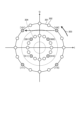
- FIG. 24 is a diagram for explaining a modulation method according to a fifth example of the fourth embodiment.
- FIG. 24 shows an IQ plane.
- the modulation method according to the fifth example of the fourth embodiment is 8QAM.
- the number of symbol points 302 is 16 on the circle 301 and 16 on the circle 304.
- the symbol point 302 may be located at [100], [101], [111], or [110] on the circle 301.
- the symbol point 302 may be located at [000], [001], [011], or [010] on the circle 304.
- the control circuit 61 moves the symbol point 302 from the position [100] to the position [101] at the timing when the symbol point 302 rotates a predetermined number of times around 16 points on the circle 301.
- FIG. 25 is a diagram for explaining a modulation scheme according to a sixth example of the fourth embodiment.
- FIG. 25 shows an IQ plane.
- the modulation scheme according to the sixth example of the fourth embodiment is 16QAM.
- the number of symbol points 302 is 16 on the circle 301 and 16 on the circle 304.
- the symbol points 302 may be located at [1000], [1001], [1011], [1010], [1100], [1101], [1111], or [1110] on the circle 301.
- the symbol points 302 may be located at [0000], [0001], [0011], [0010], [0100], [0101], [0111], or [0110] on the circle 304.
- the control circuit 61 moves the symbol point 302 from the position [1001] to the position [1010] at the timing when the symbol point 302 rotates through 16 points on the circle 301 a predetermined number of times.
- the frequency of the subcarrier signal can be set more appropriately for each modulation method.
Landscapes
- Engineering & Computer Science (AREA)
- Computer Networks & Wireless Communication (AREA)
- Signal Processing (AREA)
- Transmitters (AREA)
Abstract
Description
[通信システム]
図1を用いて、第1実施形態に係る通信システムの構成例について説明する。図1は、第1実施形態に係る通信システムの構成例を示す図である。
図2は、第1実施形態に係る送信信号および反射信号の理想環境下における信号レベルを示す図である。波形31は、親機が送信した送信信号21の信号レベルを示す。波形32Aから波形32Jは、それぞれ、子機12Aから子機12Jが反射した反射信号22の信号レベルを示す。図2に示すように、子機12Aから子機12Jが反射した反射信号22の信号レベルは、理想的には、同じである。理想環境下では、子機12Aから子機12Jは、それぞれ、他の子機12が反射した反射信号22に妨害されることなく、親機10と適切に通信することができる。
図4を用いて、第1実施形態に係る子機の構成例について説明する。図4は、第1実施形態に係る子機の構成例を示すブロック図である。
図5を用いて、第1実施形態に係るインピーダンス回転回路の構成例について説明する。図5は、第1実施形態に係るインピーダンス回転回路の構成例を示す図である。
次に、第1実施形態に係る反射信号の変調速度を変更する方法について説明する。図8を用いて、第1実施形態に係るバックスキャッタ通信における信号波形について説明する。図8は、第1実施形態に係るバックスキャッタ通信の通常時のバックスキャッタ通信における信号波形を示す図である。
図9は、第1実施形態の第1の例に係るバックスキャッタ通信における信号波形を示す図である。図10は、第1実施形態の第1の例に係るサブキャリア信号の信号波形を示す図である。図9において、キャリア信号211は、親機10からの送信信号の信号レベルを示し、サブキャリア信号212は、子機12からのサブキャリア信号の信号レベルを示す。サブキャリア信号212の周波数は、+800[kHz]である。図10に示すように、サブキャリア信号212のシンボルレートは、50[kHz]である。すなわち、図9に示す例では、通常時に比べて、サブキャリア信号のシンボルレートが、100[kHz]から50[kHz]に変更されている。本実施形態では、制御回路61は、インピーダンス回転回路62を制御することで、シンボルレートを変更する。
シンボル点の回転数=サブキャリア信号の周波数/シンボルレート・・・(1)
図12は、第1実施形態の第2の例に係るバックスキャッタ通信における信号波形を示す図である。図13は、第1実施形態の第2の例に係るサブキャリア信号の信号波形を示す図である。図12において、キャリア信号221は、親機10からの送信信号の信号レベルを示し、サブキャリア信号222は、子機12からのサブキャリア信号の信号レベルを示す。サブキャリア信号222の周波数は、+800[kHz]である。図13に示すように、サブキャリア信号222のシンボルレートは、100[kHz]である。
図14は、第1実施形態の第3の例に係るバックスキャッタ通信における信号波形を示す図である。図15は、第1実施形態の第3の例に係るサブキャリア信号の信号波形を示す図である。図14において、キャリア信号231は、親機10からの送信信号の信号レベルを示し、サブキャリア信号232は、子機12からのサブキャリア信号の信号レベルを示す。サブキャリア信号232の周波数は、+800[kHz]である。図15に示すように、サブキャリア信号232のシンボルレートは、200[kHz]である。
第2実施形態について説明する。所望の周波数を持つサブキャリア信号を生成するためには、所定の周波数を持つ元の信号が必要である。そこで、第2実施形態では、図4に示すPLL回路63が制御回路61に出力する発振信号(クロック信号)に基づいて、サブキャリア信号の周波数を制御する。
サブキャリア信号の周波数=発振信号の周波数/シンボル点数・・・(2)
第3実施形態について説明する。サブキャリア信号をPLL回路63の発振信号に基づいて生成する場合、PLL回路63の設計によっては所望の周波数を持つサブキャリア信号を生成できないこともあり得る。そこで、第3実施形態は、発振信号でサブキャリア信号の周波数を算出し、かつシンボル点数を制御することで、所望の周波数を持つサブキャリア信号を生成する。
第4実施形態について説明する。第4実施形態では、変調方式を変更することでも、シンボルレートを変更することができる。例えば、第1実施形態から第3実施形態では、インピーダンス回転回路62は、インピーダンス回路を1つのみ備えていることから、同一振幅上のシンボル点を使用している。この場合、シンボル点数が16個だとすると、BPSK(Binary Phase Shift Keying)、QPSK(Quadrature Phase Shift Keying)、8PSK(8 Phase Shift Keying)、16PSK(16 Phase Shift Keying)の変調方式に対応することができる。ここで、サブキャリア信号の振幅方向にシンボルを用意できれば、QAM(Quadrature Amplitude Modulation)変調も対応可能になる。そこで、第4実施形態では、反射係数の異なる複数のインピーダンス回路を追加し、QAM変調にも対応可能とした。
図19を用いて、第4実施形態に係るインピーダンス回転回路の構成例について説明する。図19は、第4実施形態に係るインピーダンス回転回路の構成例を示す図である。
図20は、第4実施形態の第1の例に係る変調方式を説明するための図である。図20は、IQ平面を示している。第4実施形態の第1の例に係る変調方式は、BPSKである。図20に示す例では、シンボル点302の数は、16個である。BPSKでは、シンボル点302は、IQ平面上において、[1]または[0]の位置に位置し得る。図20に示す例では、制御回路61は、シンボル点302が16個の点を所定回数回転したタイミングで、[1]の位置から[0]の位置に移動させる。
図21は、第4実施形態の第2の例に係る変調方式を説明するための図である。図20は、IQ平面を示している。第4実施形態の第2の例に係る変調方式は、QPSKである。図20に示す例では、シンボル点302の数は、16個である。QPSKでは、シンボル点302は、IQ平面上において、[11]、[10]、[00]、または[01]の位置に位置し得る。図21に示す例では、制御回路61は、シンボル点302が16個の点を所定回数回転したタイミングで、[11]の位置から[00]の位置に移動させる。
図22は、第4実施形態の第3の例に係る変調方式を説明するための図である。図22は、IQ平面を示している。第4実施形態の第3の例に係る変調方式は、8PSKである。図22に示す例では、シンボル点302の数は、16個である。8PSKでは、シンボル点302は、IQ平面上において、[000]、[001]、[011]、[010]、[100]、[101]、[111]、または[110]の位置に位置し得る。図22に示す例では、制御回路61は、シンボル点302が16個の点を所定回数回転したタイミングで、[001]の位置から[101]の位置に移動させる。
図23は、第4実施形態の第4の例に係る変調方式を説明するための図である。図23は、IQ平面を示している。第4実施形態の第4の例に係る変調方式は、16PSKである。図23に示す例では、シンボル点302の数は、16個である。16PSKでは、シンボル点302は、IQ平面上において、[0000]、[0001]、[0011]、[0010]、[0100]、[0101]、[0111]、[0110]、[1000]、[1001]、[1011]、[1010]、[1100]、[1101]、[1111]、または[1110]の位置に位置し得る。図23に示す例では、制御回路61は、シンボル点302が16個の点を所定回数回転したタイミングで、[0011]の位置から[1011]の位置に移動させる。
図24は、第4実施形態の第5の例に係る変調方式を説明するための図である。図24は、IQ平面を示している。第4実施形態の第5の例に係る変調方式は、8QAMである。図24に示す例では、シンボル点302の数は、円301上に16個、円304上に16個である。8QAMでは、シンボル点302は、円301上の[100]、[101]、[111]、または[110]に位置し得る。または、シンボル点302は、円304上の[000]、[001]、[011]、[010]に位置し得る。図24に示す例では、制御回路61は、シンボル点302が円301上の16個の点を所定回数回転したタイミングで、[100]の位置から[101]の位置に移動させる。
図25は、第4実施形態の第6の例に係る変調方式を説明するための図である。図25は、IQ平面を示している。第4実施形態の第6の例に係る変調方式は、16QAMである。図25に示す例では、シンボル点302の数は、円301上に16個、円304上に16個である。16QAMでは、シンボル点302は、円301上の[1000]、[1001]、[1011]、[1010]、[1100]、[1101]、[1111]、または[1110]に位置し得る。または、シンボル点302は、円304上の[0000]、[0001]、[0011]、[0010]、[0100]、[0101]、[0111]、または[0110]に位置し得る。図25に示す例では、制御回路61は、シンボル点302が円301上の16個の点を所定回数回転したタイミングで、[1001]の位置から[1010]の位置に移動させる。
10 親機
12 子機
40 アンテナ
41 スイッチ
42 受信回路
43 送信回路
44 制御部
45 センサ
60 CPUインターフェース
61 制御回路
62,62A インピーダンス回転回路
70 インピーダンス回路
72-1,72-2,72-3 スイッチ
73 整合回路
74 配線
75 移相器
Claims (5)
- 所定の反射係数が設定され、アンテナに接続するように構成されたインピーダンス回路を備えるインピーダンス回転回路と、
前記インピーダンス回転回路の反射係数を制御して、複素平面において、反射係数を回転するように制御する制御回路と、を含み、
前記制御回路は、通信環境に応じて前記インピーダンス回転回路の反射信号の変調速度を変更する、
伝送回路。 - 前記制御回路は、前記反射信号の変調速度と、前記反射信号のサブキャリア周波数の周波数に基づいて、回転数を制御する、
請求項1に記載の伝送回路。 - 前記インピーダンス回転回路は、クロック信号を出力するPLL回路を備え、
前記制御回路は、前記クロック信号の周波数を制御することで、前記反射信号のサブキャリア周波数を制御する、
請求項2に記載の伝送回路。 - 前記制御回路は、前記クロック信号の周波数を制御し、同一の反射係数のシンボル点数で前記反射信号のサブキャリア周波数を制御する、
請求項3に記載の伝送回路。 - 前記インピーダンス回転回路は、反射係数の異なる複数の前記インピーダンス回路を備える、
請求項4に記載の伝送回路。
Priority Applications (1)
| Application Number | Priority Date | Filing Date | Title |
|---|---|---|---|
| JP2025506914A JPWO2024190845A1 (ja) | 2023-03-15 | 2024-03-13 |
Applications Claiming Priority (2)
| Application Number | Priority Date | Filing Date | Title |
|---|---|---|---|
| JP2023041323 | 2023-03-15 | ||
| JP2023-041323 | 2023-03-15 |
Publications (1)
| Publication Number | Publication Date |
|---|---|
| WO2024190845A1 true WO2024190845A1 (ja) | 2024-09-19 |
Family
ID=92755320
Family Applications (1)
| Application Number | Title | Priority Date | Filing Date |
|---|---|---|---|
| PCT/JP2024/009897 Ceased WO2024190845A1 (ja) | 2023-03-15 | 2024-03-13 | 伝送回路 |
Country Status (2)
| Country | Link |
|---|---|
| JP (1) | JPWO2024190845A1 (ja) |
| WO (1) | WO2024190845A1 (ja) |
Citations (3)
| Publication number | Priority date | Publication date | Assignee | Title |
|---|---|---|---|---|
| US20190089571A1 (en) * | 2017-09-20 | 2019-03-21 | Qualcomm Incorporated | Adaptive Backscatter Modulation |
| JP2022056139A (ja) * | 2020-09-29 | 2022-04-08 | 国立大学法人東京工業大学 | 伝送回路 |
| JP2022127763A (ja) * | 2021-02-22 | 2022-09-01 | 富士通フロンテック株式会社 | Rfidタグリーダライタ、通信方法およびプログラム |
-
2024
- 2024-03-13 WO PCT/JP2024/009897 patent/WO2024190845A1/ja not_active Ceased
- 2024-03-13 JP JP2025506914A patent/JPWO2024190845A1/ja active Pending
Patent Citations (3)
| Publication number | Priority date | Publication date | Assignee | Title |
|---|---|---|---|---|
| US20190089571A1 (en) * | 2017-09-20 | 2019-03-21 | Qualcomm Incorporated | Adaptive Backscatter Modulation |
| JP2022056139A (ja) * | 2020-09-29 | 2022-04-08 | 国立大学法人東京工業大学 | 伝送回路 |
| JP2022127763A (ja) * | 2021-02-22 | 2022-09-01 | 富士通フロンテック株式会社 | Rfidタグリーダライタ、通信方法およびプログラム |
Also Published As
| Publication number | Publication date |
|---|---|
| JPWO2024190845A1 (ja) | 2024-09-19 |
Similar Documents
| Publication | Publication Date | Title |
|---|---|---|
| ES2646995T3 (es) | Estimación de distancia | |
| US10951446B2 (en) | Backscatter devices including examples of single sideband operation | |
| US9979462B2 (en) | Resilient virtual ground receivers | |
| US7221318B2 (en) | System and method for controlling antenna pattern | |
| EP3440454A1 (en) | Backscatter devices and systems providing backscattered signals including ofdm packets | |
| CN107925561B (zh) | 用于适配3相信号交换的方法、装置和存储介质 | |
| CN102171979B (zh) | 用于单载波和ofdm传输的代码和前导码 | |
| AU2013334523A1 (en) | Sensing distance between wireless devices using multiple scales of controlled bandwidth | |
| CN110114980A (zh) | 无线通信中的可靠的正交扩展码 | |
| US20130022058A1 (en) | Transmitter and transmission method | |
| TW200427346A (en) | Coordination of backhaul beam forming in wireless communication systems | |
| US9553695B2 (en) | Likelihood generation circuit and likelihood generation method | |
| WO2024190845A1 (ja) | 伝送回路 | |
| Blümm et al. | SDR OFDM waveform design for a UGV/UAV communication scenario | |
| WO2022070672A1 (ja) | 伝送回路 | |
| WO2020196580A1 (ja) | レーダ装置およびレーダ信号の信号処理方法 | |
| WO2012027994A1 (zh) | 微波传输装置 | |
| Xu et al. | Integrated positioning and communication relying on wireless optical OFDM | |
| JP2008538818A5 (ja) | ||
| US7912144B2 (en) | Integrated modulators and demodulators | |
| JP7851001B2 (ja) | 伝送回路 | |
| JP2014216745A (ja) | Mimo送信装置、mimo受信装置及びmimo通信システム | |
| Qiu et al. | A linear chirp wireless transmission method utilizing Doppler effect | |
| KR20160019802A (ko) | 전송 모드에 따른 레이더 신호 처리 방법 및 장치 | |
| WO2024190732A1 (ja) | 伝送回路 |
Legal Events
| Date | Code | Title | Description |
|---|---|---|---|
| 121 | Ep: the epo has been informed by wipo that ep was designated in this application |
Ref document number: 24770948 Country of ref document: EP Kind code of ref document: A1 |
|
| ENP | Entry into the national phase |
Ref document number: 2025506914 Country of ref document: JP Kind code of ref document: A |
|
| WWE | Wipo information: entry into national phase |
Ref document number: 2025506914 Country of ref document: JP |
|
| NENP | Non-entry into the national phase |
Ref country code: DE |
|
| 122 | Ep: pct application non-entry in european phase |
Ref document number: 24770948 Country of ref document: EP Kind code of ref document: A1 |