WO2024203140A1 - Détecteur magnétique - Google Patents
Détecteur magnétique Download PDFInfo
- Publication number
- WO2024203140A1 WO2024203140A1 PCT/JP2024/008898 JP2024008898W WO2024203140A1 WO 2024203140 A1 WO2024203140 A1 WO 2024203140A1 JP 2024008898 W JP2024008898 W JP 2024008898W WO 2024203140 A1 WO2024203140 A1 WO 2024203140A1
- Authority
- WO
- WIPO (PCT)
- Prior art keywords
- substrate
- diamond
- magnetic detector
- magnetic
- disposed
- Prior art date
- Legal status (The legal status is an assumption and is not a legal conclusion. Google has not performed a legal analysis and makes no representation as to the accuracy of the status listed.)
- Ceased
Links
Images




Classifications
-
- G—PHYSICS
- G01—MEASURING; TESTING
- G01N—INVESTIGATING OR ANALYSING MATERIALS BY DETERMINING THEIR CHEMICAL OR PHYSICAL PROPERTIES
- G01N24/00—Investigating or analyzing materials by the use of nuclear magnetic resonance, electron paramagnetic resonance or other spin effects
-
- G—PHYSICS
- G01—MEASURING; TESTING
- G01R—MEASURING ELECTRIC VARIABLES; MEASURING MAGNETIC VARIABLES
- G01R33/00—Arrangements or instruments for measuring magnetic variables
- G01R33/20—Arrangements or instruments for measuring magnetic variables involving magnetic resonance
Definitions
- This disclosure relates to a magnetic detector.
- Patent Document 1 discloses a sensor that measures magnetic fields and includes a diamond having an NV center and an antenna made of a loop-shaped conductor formed on its surface. In the technology described in Patent Document 1, excitation light and its fluorescence are input and output to the NV center from the surface of the sensor opposite the surface on which the antenna is formed.
- the magnetic detector comprises a diamond substrate having an NV center, a transparent first substrate on which the diamond substrate is disposed, an emitter formed on a surface of the first substrate or on a surface of the diamond substrate facing opposite to the surface on which the NV center is formed, and a second substrate having an opening and on which the first substrate is disposed, with at least a portion of the diamond substrate exposed from the opening.
- FIG. 1 is a schematic diagram illustrating an example of a magnetic detector according to a first embodiment.
- FIG. 2 is a schematic diagram illustrating an example of a substrate on which a magnetic detector is arranged.
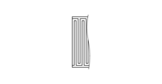
- FIG. 3A is a schematic diagram illustrating an example of a radiator.
- FIG. 3-2 is a partially enlarged view of the radiator.
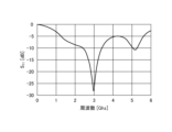
- FIG. 4 is a diagram showing the S11 reflection characteristic of a loop antenna.
- FIG. 5 is a schematic diagram illustrating an example of a magnetic detector according to the second embodiment.
- FIG. 6 is a schematic diagram illustrating an example of a magnetic detector according to the third embodiment.
- the magnetic detector 1 is for detecting magnetism generated in the measured sample 100.
- Figure 1 is a schematic diagram for explaining an example of the magnetic detector according to the first embodiment.
- the measured sample 100 is an object to be detected by the magnetic detector 1, in other words, a specimen.
- a magnetic field is generated in the measured sample 100 when a current flows through a circuit.
- the magnetic field generated in the measured sample 100 is detected by the magnetic detector 1.
- the magnetic detector 1 is disposed between an objective lens of a microscope (not shown) and a measured sample 100.
- the magnetic detector 1 includes a diamond substrate 10, a first substrate 13, a radiator 24, and a second substrate 15.
- the diamond substrate 10 is a so-called diamond sensor.
- the diamond substrate 10 has an NV center 11 formed in a diamond crystal.
- An NV center 11 is formed in the diamond crystal.
- the length of one side of the diamond crystal is, for example, 2 mm.
- the thickness of the diamond crystal is, for example, 300 ⁇ m.
- NV center 11 may be arranged singly on one face of the diamond crystal, or multiple NV centers 11 may be arranged in one direction. NV center 11 may be a crystal with multiple different orientations. NV center 11 is formed on the extreme surface of face 11b by, for example, CVD (Chemical Vapor Deposition) or ion implantation.
- CVD Chemical Vapor Deposition
- ion implantation ion implantation
- the NV centre 11 is a complex defect in a diamond crystal where carbon would normally be present, replaced by nitrogen, with a vacancy at an adjacent position.
- the NV centre 11 is missing a portion of the degenerate shared electron pair.
- the strength of the external magnetic field can be detected by detecting the electron spin resonance caused by these using light waves and microwaves.
- the electron spin resonance frequency in zero magnetic field is known to be approximately 2.87 GHz. When microwaves with the frequency of this resonance point (resonance frequency) are irradiated, the fluorescence with a wavelength of 638 nm is quenched.
- At least a portion of surface 10a of diamond substrate 10 is exposed from opening 16 of second substrate 15, which will be described later.
- surface 10a of diamond substrate 10 is entirely exposed from opening 16.
- Microwaves and green light enter from the portion of diamond substrate 10 exposed from opening 16.
- Red light exits from the portion of diamond substrate 10 exposed from opening 16.
- FIG. 1 the direction of incidence of green light is indicated by arrow LG.
- the direction of emission of red light is indicated by arrow LR.
- the direction of incidence of microwaves is indicated by arrow LM.
- Surface 10b of diamond substrate 10 is the magnetic detection surface.
- a first substrate 13 is disposed on the surface 10a side of diamond substrate 10.
- the first substrate 13 is an antenna substrate.
- the first substrate 13 is a transparent substrate.
- the first substrate 13 is a substrate that is transmissive to green light, red light, and microwaves.
- the diamond substrate 10 is disposed on the surface 13b of the first substrate 13.
- the second substrate 15 and the radiator 24 are disposed on the surface 13a of the first substrate 13.
- the first substrate 13 has an outer shape larger than the opening 16 of the second substrate 15.
- the diamond substrate 10 is bonded to the central portion of the first substrate 13 that is exposed from the opening 16.
- the outer edge of the first substrate 13 is bonded to the inner edge of the surface 15b of the second substrate 15.
- the first substrate 13 has an opening 16 and holds the diamond substrate 10 instead of the second substrate 15, which cannot directly hold the diamond substrate 10.
- the second substrate 15 is a PCB (Printed Circuit Board).
- the second substrate 15 has an opening 16 in the center.
- the first substrate 13 is disposed in the center of the second substrate 15.
- the outer edge of the first substrate 13 is joined to the inner edge of the surface 15b of the second substrate 15.
- the top view is a view along the direction of incidence of the green light.
- the top view is a view of the magnetic detector 1 from the side opposite the magnetic detection surface.
- the dashed line indicates the viewing angle V of the objective lens, that is, the NA (Numerical Aperture) and the working distance. If the opening 16 of the second substrate 15 is narrower than the viewing angle V, a part of the excitation light incident from the objective lens is blocked by the second substrate 15, reducing the amount of light and the detection sensitivity. Therefore, the size of the opening 16 of the second substrate 15 is set so that the excitation light incident from the objective lens is not blocked, in other words, so that the viewing angle A is not blocked. As a result, the excitation light and microwaves are appropriately incident from the surface 10a of the diamond substrate 10 through the opening 16 of the second substrate 15, and act on the NV center 11 on the surface 10b side, which is the magnetic detection surface.
- the second substrate 15 is provided with a high-frequency transmission line that supplies microwaves to the radiator 24.
- the high-frequency transmission line will be described later.
- the diamond substrate 10 when measuring the magnetic field of the sample 100 to be measured, the diamond substrate 10, the first substrate 13, and the second substrate 15 are stacked in that order, starting from the substrate closest to the sample 100 to be measured.
- the microwave power supply system supplies microwaves in the magnetic detector 1.
- the microwave power supply system is a radiator 24.
- the radiator 24 is provided on the surface 13a of the first substrate 13.
- the radiator 24 applies microwaves to the NV center 11 of the diamond substrate 10.
- the radiator 24 transmits microwaves to be irradiated to the NV center 11 of the diamond substrate 10.
- the radiator 24 transmits microwaves from a microwave source (not shown).
- a high-frequency transmission line provided on the second substrate 15 is connected to the radiator 24, and microwaves are supplied from the outside.
- the radiator 24 is, for example, a micro loop antenna.
- the frequency of the radiator 24 is, for example, 2.8 GHz or more and 2.9 GHz or less.
- the input power of the radiator 24 is, for example, -20 dBm or more and +20 dBm or less.
- the radiator 24 may be arranged in a comb-like shape as shown in FIG. 3-2.
- the comb-tooth portion forms a capacitance. By adjusting the line and space of the electrode elements and the number of pairs, the comb-tooth portion can reduce the reflection of microwaves of a specific frequency that are incident on the radiator 24.
- the optical system detects the magnetism of the measured sample 100 in the magnetic detector 1.
- the optical system is a light-emitting element and a light-receiving element, not shown.
- the light-emitting element and the light-receiving element are arranged, for example, on an objective lens arranged facing the diamond substrate 10.
- the light-emitting element and the light-receiving element are focused on the NV center 11 provided on the diamond substrate 10.
- the light-emitting element irradiates the diamond substrate 10 with green light.
- the light-emitting element emits excitation light that irradiates the diamond crystal.
- the light-emitting element is, for example, a laser diode.
- the light-emitting element emits laser light with a wavelength of, for example, 527 nm.
- the light-emitting element emits green excitation light.
- a green light-emitting diode LED: Light Emitting Diode
- VCSEL Vertical Cavity Surface Emitting Laser
- LD Green Edge-emitting laser diode
- the light receiving element receives the red light generated by inputting green light to the diamond substrate 10.
- the light receiving element detects the fluorescence of the diamond substrate 10.
- the light receiving element is a photodiode.
- the light receiving element receives the fluorescence emitted from the diamond crystal by the excitation light.
- a Si-PIN photodiode PD: Photo Diode
- an InGaAs-PIN photodiode can be used as the light receiving element.
- FIG. 2 is a schematic diagram illustrating an example of a substrate on which a magnetic detector is disposed.
- Fig. 3-1 is a schematic diagram illustrating an example of a radiator.
- Fig. 3-2 is a partially enlarged view of the radiator.
- the magnetic detector 1 configured in this manner is disposed on a substrate 50.
- the substrate 50 is a PCB.
- the second substrate 15 of the magnetic detector 1 and the substrate 50 may be a single substrate or may be separate substrates.
- a microwave power supply system including a high-frequency connector 51, a high-frequency transmission line 52, a high-frequency transmission line 53, a high-frequency transmission line 54, and a high-frequency transmission line 55 are arranged on the substrate 50.
- the width of the end 54a of the high-frequency transmission line 54 gradually tapers toward the connection with the second substrate 15.
- a method of detecting the magnetic field of the sample 100 to be measured in the magnetic detector 1 will be described below.
- the sample 100 to be measured is placed close to or in close contact with the surface 10b of the diamond substrate 10 of the magnetic detector 1, which is the magnetic field acting surface.
- the microwaves generated by the microwave source propagate to the radiator 24 through the high-frequency connector 51, high-frequency transmission line 52, high-frequency transmission line 53, high-frequency transmission line 54, and high-frequency transmission line 55.
- the microwaves are then radiated from the radiator 24.
- the microwaves radiated from the radiator 24 act on the NV center 11 of the diamond substrate 10, causing electron spin resonance.
- the spatial change in the direction or magnitude of the magnetic field generated in the measured sample 100 acts on the NV center 11 of the diamond crystal of the diamond substrate 10 of the magnetic detector 1.
- the green excitation light from the light-emitting element is incident on the diamond crystal.
- the green excitation light that is incident on the diamond crystal then diffuses widely within the diamond crystal, irradiating and exciting the NV center 11.
- the excited NV center 11 generates red fluorescence, which enters the diamond crystal.
- the red fluorescence then diffuses widely within the diamond crystal and enters the light receiving surface of the light receiving element.
- the light receiving element receives the electron spin resonance signal of the NV center 11 excited by the excitation light from the diamond crystal as fluorescence.
- Fig. 4 is a diagram showing the S11 reflection characteristic of the loop antenna.
- the diamond substrate 10 is exposed from the opening 16 of the second substrate 15.
- the radiator 24 is provided on the surface of the first substrate 13 or on the surface of the diamond substrate 10 facing the opposite side to the magnetic detection surface.
- an optical system or a microwave power supply system is not arranged on the surface 10b side, which is the magnetic detection surface of the diamond substrate 10.
- power can be supplied to the radiator 24 from the surface 10a opposite to the surface 10b, which is the magnetic detection surface, via the second substrate 15.
- the measured sample 100 of various shapes can be brought close to the surface 10b, which is the magnetic detection surface. In this way, according to this embodiment, a magnetic field can be detected with high sensitivity.
- the magnetic detector 1 when the magnetic detector 1 is applied to a microscope, the field of view of the objective lens is sufficiently secured, making it easier to optically bring the NV center 11 into the field of view.
- This embodiment can be used for observing the magnetic field of a flat microcircuit, etc.
- the diamond substrate 10, the first substrate 13, and the second substrate 15 are stacked in that order, starting from the substrate closest to the measured sample 100.
- the measured samples 100 of various shapes can be brought close to the surface 10b, which is the magnetic detection surface.
- the diamond substrate 10 can be placed without any restrictions on thickness.
- the radiator 24 is disposed on the first substrate 13.
- the antenna forming surface can be disposed along the surface of the second substrate 15. According to this embodiment, there is no need to provide a through hole or the like in the second substrate 15, and therefore the configuration can be easily performed.
- the surface on which the antenna is formed is the magnetic detection surface.
- the wiring that supplies power to the antenna from the outside of the diamond forms a convex portion on the magnetic detection surface side. This can make it difficult to bring the sample to be measured close to the magnetic detection surface. If the sample to be measured cannot be brought close enough to the magnetic detection surface, the detection sensitivity of the magnetic field decreases.
- [Second embodiment] 5 is a schematic diagram for explaining an example of a magnetic detector according to the second embodiment.
- a diamond substrate 10, a first substrate 13, and a second substrate 15 are different from those in the first embodiment.
- the diamond substrate 10 and the second substrate 15 are disposed on the surface 13b of the first substrate 13.
- the diamond substrate 10 is disposed inside the opening 16 of the second substrate 15.
- the diamond substrate 10 may protrude beyond the surface 13b of the first substrate 13.
- the emitter 24 is disposed between the diamond substrate 10 and the first substrate 13. More specifically, the emitter 24 is provided on the surface 13b of the first substrate 13 or the surface 10a of the diamond substrate 10.
- the diamond substrate 10 and the second substrate 15 are disposed on the surface 13b of the first substrate 13.
- the diamond substrate 10 is disposed inside the opening 16 of the second substrate 15.
- the thickness of the magnetic detector 1 can be made thinner than in the first embodiment.
- the objective lens can be brought closer to the NV center 11 of the diamond substrate 10.
- the radiator 24 is disposed between the diamond substrate 10 and the first substrate 13.
- power can be supplied to the radiator 24 from the surface 10a opposite the surface 10b, which is the magnetic detection surface.
- the measured sample 100 when the diamond substrate 10 protrudes beyond the surface 13b of the first substrate 13, the measured sample 100 can be brought close to or in close contact with the surface 10b, which is the magnetic field acting surface of the diamond substrate 10 of the magnetic detector 1.
- This embodiment allows the measured samples 100 of various shapes to be brought close to the surface 10b, which is the magnetic detection surface. In this way, this embodiment allows magnetic fields to be detected with high sensitivity.
- FIG. 6 is a schematic diagram illustrating an example of a magnetic detector according to a third embodiment.
- the magnetic detector 1 is different from the first embodiment in that it includes a magnet 30.
- the magnet 30 applies a static magnetic field to the NV center 11 of the diamond substrate 10.
- the magnet 30 is disposed on the first substrate 13 or the second substrate 15.
- the magnet 30 is adjusted so that the direction AM of the magnetic field is perpendicular to the direction AD of the NV center 11.
- the magnet 30 can be fixed onto the surface 13b of the first substrate 13. According to this embodiment, double resonance can be stably and accurately generated by the magnet 30. This embodiment can measure the magnetic field more accurately.
Landscapes
- Physics & Mathematics (AREA)
- General Physics & Mathematics (AREA)
- Chemical & Material Sciences (AREA)
- High Energy & Nuclear Physics (AREA)
- Health & Medical Sciences (AREA)
- Life Sciences & Earth Sciences (AREA)
- Condensed Matter Physics & Semiconductors (AREA)
- Analytical Chemistry (AREA)
- Biochemistry (AREA)
- General Health & Medical Sciences (AREA)
- Immunology (AREA)
- Pathology (AREA)
- Measuring Magnetic Variables (AREA)
Abstract
Priority Applications (1)
| Application Number | Priority Date | Filing Date | Title |
|---|---|---|---|
| JP2025510185A JP7823855B2 (ja) | 2023-03-29 | 2024-03-07 | 磁気検出器 |
Applications Claiming Priority (2)
| Application Number | Priority Date | Filing Date | Title |
|---|---|---|---|
| JP2023-054219 | 2023-03-29 | ||
| JP2023054219 | 2023-03-29 |
Publications (1)
| Publication Number | Publication Date |
|---|---|
| WO2024203140A1 true WO2024203140A1 (fr) | 2024-10-03 |
Family
ID=92904374
Family Applications (1)
| Application Number | Title | Priority Date | Filing Date |
|---|---|---|---|
| PCT/JP2024/008898 Ceased WO2024203140A1 (fr) | 2023-03-29 | 2024-03-07 | Détecteur magnétique |
Country Status (2)
| Country | Link |
|---|---|
| JP (1) | JP7823855B2 (fr) |
| WO (1) | WO2024203140A1 (fr) |
Cited By (1)
| Publication number | Priority date | Publication date | Assignee | Title |
|---|---|---|---|---|
| WO2025187461A1 (fr) * | 2024-03-07 | 2025-09-12 | 京セラ株式会社 | Détecteur et microscope |
Citations (5)
| Publication number | Priority date | Publication date | Assignee | Title |
|---|---|---|---|---|
| US20160282427A1 (en) * | 2014-02-19 | 2016-09-29 | Infinitum Solutions, Inc. | Integrated optical nanoscale probe measurement of electric fields from electric charges in electronic devices |
| JP2021103093A (ja) * | 2019-12-24 | 2021-07-15 | スミダコーポレーション株式会社 | 測定装置および測定方法 |
| WO2021200144A1 (fr) * | 2020-03-31 | 2021-10-07 | 国立大学法人東京工業大学 | Dispositif de mesure d'état physique |
| JP2022098572A (ja) * | 2020-12-22 | 2022-07-04 | 矢崎総業株式会社 | センサ |
| WO2022249995A1 (fr) * | 2021-05-25 | 2022-12-01 | 京セラ株式会社 | Substrat de détection, détecteur et dispositif de détection |
-
2024
- 2024-03-07 WO PCT/JP2024/008898 patent/WO2024203140A1/fr not_active Ceased
- 2024-03-07 JP JP2025510185A patent/JP7823855B2/ja active Active
Patent Citations (5)
| Publication number | Priority date | Publication date | Assignee | Title |
|---|---|---|---|---|
| US20160282427A1 (en) * | 2014-02-19 | 2016-09-29 | Infinitum Solutions, Inc. | Integrated optical nanoscale probe measurement of electric fields from electric charges in electronic devices |
| JP2021103093A (ja) * | 2019-12-24 | 2021-07-15 | スミダコーポレーション株式会社 | 測定装置および測定方法 |
| WO2021200144A1 (fr) * | 2020-03-31 | 2021-10-07 | 国立大学法人東京工業大学 | Dispositif de mesure d'état physique |
| JP2022098572A (ja) * | 2020-12-22 | 2022-07-04 | 矢崎総業株式会社 | センサ |
| WO2022249995A1 (fr) * | 2021-05-25 | 2022-12-01 | 京セラ株式会社 | Substrat de détection, détecteur et dispositif de détection |
Cited By (1)
| Publication number | Priority date | Publication date | Assignee | Title |
|---|---|---|---|---|
| WO2025187461A1 (fr) * | 2024-03-07 | 2025-09-12 | 京セラ株式会社 | Détecteur et microscope |
Also Published As
| Publication number | Publication date |
|---|---|
| JPWO2024203140A1 (fr) | 2024-10-03 |
| JP7823855B2 (ja) | 2026-03-04 |
Similar Documents
| Publication | Publication Date | Title |
|---|---|---|
| US8634078B2 (en) | Sensor, method for detecting the presence and/or concentration of an analyte using the sensor, and use of the method | |
| US12442872B2 (en) | Magnetic field gradiometer | |
| US20240219486A1 (en) | Detection substrate, detector, and detecting device | |
| JP7585341B2 (ja) | 磁気センサ及び検出システム | |
| JP7823855B2 (ja) | 磁気検出器 | |
| US12372487B2 (en) | Sensor device for magnetic field measurement by means of optical magnetic resonance measurement | |
| US12523721B2 (en) | Diamond magnetic sensor unit and diamond magnetic sensor system | |
| WO2022163679A1 (fr) | Unité de capteur de diamant | |
| US20240111008A1 (en) | Diamond sensor unit and diamond sensor system | |
| CN114706022A (zh) | 一种探头装置以及磁力计 | |
| US20220166185A1 (en) | Semiconductor laser device | |
| EP4302014B1 (fr) | Procédés et appareil permettant d'intégrer un diamant ayant une del vers une détection quantique sur puce | |
| US7385393B2 (en) | Magnetic field measuring apparatus capable of measuring at high spatial resolution | |
| JP7428322B2 (ja) | 励起光照射装置および励起光照射方法 | |
| JP7397429B2 (ja) | 励起光照射装置および励起光照射方法 | |
| WO2025187461A1 (fr) | Détecteur et microscope | |
| US11733264B2 (en) | Cantilever, scanning probe microscope, and measurement method using scanning probe microscope | |
| JP7813016B2 (ja) | 磁場検出装置 | |
| WO2024181575A1 (fr) | Capteur de courant et dispositif de détection de courant | |
| US20250116734A1 (en) | Sensor system for detecting a medium | |
| JP3143884B2 (ja) | 発光走査型トンネル顕微鏡 | |
| JP7854568B2 (ja) | 電流センサ及び電流検出装置 | |
| CN111121962A (zh) | 光纤式光电探测器、探测系统、测试系统及制备方法 | |
| JP2026066773A (ja) | センサ | |
| JP2026066774A (ja) | センサ |
Legal Events
| Date | Code | Title | Description |
|---|---|---|---|
| 121 | Ep: the epo has been informed by wipo that ep was designated in this application |
Ref document number: 24779274 Country of ref document: EP Kind code of ref document: A1 |
|
| ENP | Entry into the national phase |
Ref document number: 2025510185 Country of ref document: JP Kind code of ref document: A |
|
| WWE | Wipo information: entry into national phase |
Ref document number: 2025510185 Country of ref document: JP |
|
| NENP | Non-entry into the national phase |
Ref country code: DE |
|
| 122 | Ep: pct application non-entry in european phase |
Ref document number: 24779274 Country of ref document: EP Kind code of ref document: A1 |