WO2024214655A1 - Boîtier de capteur et procédé de fabrication d'un boîtier de capteur - Google Patents
Boîtier de capteur et procédé de fabrication d'un boîtier de capteur Download PDFInfo
- Publication number
- WO2024214655A1 WO2024214655A1 PCT/JP2024/014163 JP2024014163W WO2024214655A1 WO 2024214655 A1 WO2024214655 A1 WO 2024214655A1 JP 2024014163 W JP2024014163 W JP 2024014163W WO 2024214655 A1 WO2024214655 A1 WO 2024214655A1
- Authority
- WO
- WIPO (PCT)
- Prior art keywords
- chip
- sensor package
- flat
- sensor
- insulating film
- Prior art date
- Legal status (The legal status is an assumption and is not a legal conclusion. Google has not performed a legal analysis and makes no representation as to the accuracy of the status listed.)
- Ceased
Links
Images


Classifications
-
- G—PHYSICS
- G01—MEASURING; TESTING
- G01N—INVESTIGATING OR ANALYSING MATERIALS BY DETERMINING THEIR CHEMICAL OR PHYSICAL PROPERTIES
- G01N27/00—Investigating or analysing materials by the use of electric, electrochemical, or magnetic means
- G01N27/02—Investigating or analysing materials by the use of electric, electrochemical, or magnetic means by investigating impedance
- G01N27/04—Investigating or analysing materials by the use of electric, electrochemical, or magnetic means by investigating impedance by investigating resistance
- G01N27/12—Investigating or analysing materials by the use of electric, electrochemical, or magnetic means by investigating impedance by investigating resistance of a solid body in dependence upon absorption of a fluid; of a solid body in dependence upon reaction with a fluid, for detecting components in the fluid
- G01N27/125—Composition of the body, e.g. the composition of its sensitive layer
-
- G—PHYSICS
- G01—MEASURING; TESTING
- G01N—INVESTIGATING OR ANALYSING MATERIALS BY DETERMINING THEIR CHEMICAL OR PHYSICAL PROPERTIES
- G01N33/00—Investigating or analysing materials by specific methods not covered by groups G01N1/00 - G01N31/00
- G01N33/0004—Gaseous mixtures, e.g. polluted air
- G01N33/0009—General constructional details of gas analysers, e.g. portable test equipment
- G01N33/0027—General constructional details of gas analysers, e.g. portable test equipment concerning the detector
- G01N33/0036—General constructional details of gas analysers, e.g. portable test equipment concerning the detector specially adapted to detect a particular component
- G01N33/005—H2
-
- H—ELECTRICITY
- H10—SEMICONDUCTOR DEVICES; ELECTRIC SOLID-STATE DEVICES NOT OTHERWISE PROVIDED FOR
- H10W—GENERIC PACKAGES, INTERCONNECTIONS, CONNECTORS OR OTHER CONSTRUCTIONAL DETAILS OF DEVICES COVERED BY CLASS H10
- H10W74/00—Encapsulations, e.g. protective coatings
Definitions
- This disclosure relates to a sensor package and a method for manufacturing the sensor package.
- Patent Document 1 discloses a sensor device that includes a chip having a detection structure, a lead frame, bonding wires, a package, etc.
- Patent Document 1 has a problem with the quality of the sensor unit deteriorating.
- the present disclosure provides a sensor package etc. that can prevent deterioration of the quality of the sensor unit.
- a sensor package includes a chip having an exposed portion of a sensor unit on its surface, a substrate on which the chip is mounted, and a molded resin portion formed to cover the surface of the chip excluding the exposed portion and the surface of the substrate, the molded resin portion having an opening hole located on the exposed portion, the chip having a flat portion on the surface of the chip that is located outside the exposed portion, and the edge of the opening hole on the surface side of the chip is formed along the flat portion.
- a sensor package includes a chip having an exposed portion of a sensor unit on its surface, a substrate on which the chip is mounted, and a molded resin portion formed to cover the surface of the chip excluding the exposed portion and the surface of the substrate, the molded resin portion having an opening hole located on the exposed portion, and the edge of the opening hole on the surface side of the chip being located on the same plane as the surface side of the chip.
- a method of manufacturing a sensor package includes the steps of forming a flat portion on the surface of a chip, mounting the chip on the surface of a substrate, and arranging a protruding portion of a mold above an exposed portion of the sensor portion of the chip and forming a molded resin portion to cover the surface of the chip excluding the exposed portion and the surface of the substrate, wherein in the step of forming the flat portion, the flat portion is provided outside the area in which the exposed portion is formed, and in the step of forming the molded resin portion, the mold is positioned so that the edge of the protruding portion is positioned on the flat portion to form the molded resin portion.
- This disclosure makes it possible to prevent deterioration of the quality of the sensor part of the sensor package.
- FIG. 1 is a cross-sectional view showing a sensor package of Comparative Example 1.
- FIG. 2 is a diagram showing protrusions and the like of a mold used when resin-molding the sensor package of Comparative Example 1.
- FIG. 3 is a diagram showing the wiring and insulating film on the top layer of the chip of the sensor package of Comparative Example 2.
- FIG. 4 is a cross-sectional view taken along line IV-IV in FIG.
- FIG. 5 is a diagram showing an example of a problem that occurs in the sensor package of Comparative Example 2.
- FIG. 6 is a schematic diagram of a sensor package according to the first embodiment.
- FIG. 7 is a diagram showing a cross section of the chip and the mold resin part of the sensor package according to the first embodiment.
- FIG. 8 is a top view of the flat portion of the chip of the first embodiment.
- FIG. 9 is a diagram showing another example of the flat portion of the chip according to the first embodiment.
- FIG. 10 is a diagram showing a cross section of a sensor portion of the sensor package according to the first embodiment.
- FIG. 11 is a flowchart showing a method for manufacturing the sensor package according to the first embodiment.
- FIG. 12 is a diagram showing a cross section of a chip and a mold resin part of a sensor package according to a first modification of the first embodiment.
- FIG. 13 is a diagram showing a cross section of a chip and a molded resin part of a sensor package according to the second modification of the first embodiment.
- FIG. 14 is a top view of a flat portion of a chip according to the second modification of the first embodiment.
- FIG. 15 is a diagram showing another example of the flat portion of the chip according to the second modification of the first embodiment.
- FIG. 16 is a diagram showing a cross section of a chip and a mold resin part of a sensor package according to the third modification of the first embodiment.
- FIG. 17 is a diagram showing a cross section of a chip and a mold resin part of a sensor package according to the fourth modification of the first embodiment.
- FIG. 18 is a diagram showing a cross section of a chip and a mold resin part of a sensor package according to the fifth modification of the first embodiment.
- FIG. 19 is a diagram showing a cross section of a chip and a mold resin part of a sensor package according to the sixth modification of the first embodiment.
- FIG. 20 is a top view of the flat portion of the chip according to the sixth modification of the first embodiment.
- FIG. 21 is a diagram showing a cross section of a chip and a mold resin part of a sensor package according to the seventh modification of the first embodiment.
- FIG. 22 is a top view of the flat portion of the chip according to the seventh modification of the first embodiment.
- FIG. 23 is a diagram showing a cross section of a chip and a mold resin part of a sensor package according to the eighth modification of the first embodiment.
- FIG. 24 is a diagram showing a guide groove of a tip according to the eighth modification of the first embodiment.
- FIG. 25 is a diagram showing another example of the guide groove of the tip according to the eighth modification of the first embodiment.
- FIG. 26 is a diagram showing a cross section of a chip and a molded resin part of a sensor package according to a ninth modification of the first embodiment.
- FIG. 27 is a top view of a flat portion of a chip of a sensor package according to a tenth modification of the first embodiment.
- FIG. 28 is a top view of a flat portion of a chip of a sensor package according to an eleventh modification of the first embodiment.
- FIG. 29 is a diagram showing a cross section of a via conductor of a chip in a sensor package according to a twelfth modification of the first embodiment.
- FIG. 30 is a diagram showing a cross section of another example of a via conductor.
- FIG. 31 is a top view of the via conductor.
- FIG. 32 is a diagram showing a cross section of the chip and the mold resin part of the sensor package according to the second embodiment.
- FIG. 33 is a top view of a flat portion of a chip in a sensor package according to the second embodiment.
- FIG. 34 is a diagram showing another example of the flat portion of the chip according to the second embodiment.
- FIG. 35 is a diagram showing a cross section of a chip and a molded resin part of a sensor package according to a first modification of the second embodiment.
- FIG. 36 is a diagram showing a cross section of a sensor package and a protruding portion of a mold according to the second modification of the second embodiment.
- FIG. 37 is a plan view showing the guide grooves of the protrusions of the mold.
- FIG. 38 is a diagram showing another example of the guide groove in the protrusion of the mold.
- FIG. 39 is a flowchart showing a method for manufacturing a sensor package according to the second embodiment.
- FIG. 40 is a top view of a flat portion of a chip of a sensor package according to a modification of the first and second embodiments.
- FIG. 1 is a cross-sectional view showing a sensor package 510 of Comparative Example 1.
- the sensor package 510 of Comparative Example 1 includes a substrate 520, a chip 530 arranged on the substrate 520, a wire 550 that electrically connects the substrate 520 and the chip 530, and a molded resin part 560 formed on the substrate 520 so as to cover a part of the chip 530 and the wire 550.
- the figure also shows an external terminal 570.
- an opening hole 562 is formed in the molded resin part 560 to expose the sensor part 600 provided on the surface of the chip 530.
- the opening hole 562 in the molded resin part 560 is formed by a protrusion 92 that protrudes inward from the mold 90.
- FIG. 2 shows the protrusion 92 of the mold 90 used when resin molding the sensor package 510 of Comparative Example 1.
- the molded resin part 560 is formed, for example, by covering the substrate 520, the chip 530 and the wires 550 with a cavity-shaped metal mold 90 and molding the resin.
- a film-shaped resin sheet may be placed along the inner surface of the metal mold 90.
- the opening hole 562 is formed by injecting a resin material into the metal mold 90 while pressing the protruding part 92 of the metal mold 90 against the surface of the chip 530.
- FIG. 3 is a diagram showing the positions of the wiring 533 and insulating film 535 on the top layer of the chip 530 of the sensor package 510A of Comparative Example 2.
- FIG. 4 is a diagram showing a cross section of line IV-IV in FIG. 3.
- FIG. 3(a) shows a plan view of the sensor package 510A of Comparative Example 2, and (b) shows a cross-sectional view of the sensor package 510A.
- FIG. 4 shows multiple top-layer wirings 533 formed on the surface of the chip 530, and an insulating film 535 formed on the surface of the chip 530 so as to cover the multiple top-layer wirings 533.
- the multiple top layer wirings 533 are arranged in islands scattered across the surface of the chip 530. Therefore, the insulating film 535 is formed with projections and recesses corresponding to the positions of the multiple top layer wirings 533 (see FIG. 4). Therefore, when the protruding portion 92 of the mold 90 is pressed against the uneven surface 535a of the insulating film 535 to mold the resin, the following problems may occur.
- FIG. 5 shows an example of a problem that occurs in the sensor package 510A of Comparative Example 2.
- FIG. 5(a) shows an example where resin leakage has occurred
- FIG. 5(b) shows an example where cracks have occurred.
- the opening hole 562 is formed by molding the resin while pressing the protruding portion 92 of the mold 90 against the insulating film 535 of the chip 530, but the strong pressure generated inside the mold 90 causes the resin material to seep into the sensor section 600 through the gaps in the unevenness of the insulating film 535. In that case, as shown in FIG. 5(a), the resin material comes into contact with the sensor section 600, causing a problem of a decrease in the detection accuracy of the sensor section 600.
- the sensor package etc. disclosed herein has the following configuration to prevent deterioration of the quality of the sensor part.
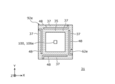
- FIG. 6 is a schematic diagram of the sensor package 10 according to the first embodiment.
- FIG. 6(a) shows a plan view of the sensor package 10
- FIG. 6(b) shows a cross-sectional view taken along line VIb-VIb in FIG. 6(a).
- the sensor package 10 includes a substrate 20, a chip 30 mounted on the substrate 20, and a molded resin portion 60 provided on the chip 30 and the substrate 20.
- the substrate 20 is, for example, a resin substrate or a ceramic substrate, and has a plate-like shape.
- the substrate 20 has a front surface 21 and a back surface 22 facing away from the front surface 21.
- the front surface 21 and the back surface 22 are each flat and parallel to each other. When viewed from a direction perpendicular to the front surface 21, the substrate 20 has a rectangular shape.
- the substrate 20 has a plurality of wirings and a plurality of pad electrodes, and the wirings are formed so as to electrically connect external terminals on the back surface 22 side and pad electrodes on the front surface 21 side (not shown).
- the substrate 20 is not limited to a resin substrate or a ceramic substrate, and may be a lead frame.
- a lead frame has small thickness variation, which can reduce thickness variation in the members (substrate, adhesive layer, and chip) sandwiched between the lower mold and the protruding portion 92 of the upper mold.
- the substrate 20 is a lead frame, the die pad portion and pad portion are arranged separately in an island shape, and each island may be arranged within a rectangular area.
- the shape of the lead frame substrate including the resin and the leads is rectangular.
- Chip 30 is a semiconductor chip, and has a rectangular and plate-like shape. The area of chip 30 is smaller than the area of substrate 20. Chip 30 has a front surface 31 and a back surface 32 facing away from front surface 31. Chip 30 is disposed on substrate 20 so that back surface 32 faces front surface 21 of substrate 20. Note that in the cross-sectional view of FIG. 6(b), the bonding layer (e.g., a die bond agent or die bonding film tape) is omitted. This is the same for the subsequent cross-sectional views.
- the bonding layer e.g., a die bond agent or die bonding film tape
- the chip 30 has a sensor unit 100 for detecting the environmental condition (e.g., air quality) of the space in which the sensor package 10 is placed.
- the sensor unit 100 is, for example, a hydrogen sensor that detects hydrogen.
- the sensor unit 100 may also be an environmental sensor that detects temperature, humidity, gas concentration, or airflow.
- the exposed portion 106e of the sensor unit 100 is provided on the surface 31 of the chip 30.
- the exposed portion 106e is provided in the center of the chip 30 at a position corresponding to the opening hole 62 of the molded resin part 60.
- the exposed portion 106e of the sensor unit 100 is located inside the side of the opening hole 62.
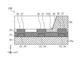
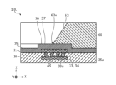
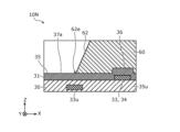
- FIG. 7 is a diagram showing a cross section of the chip 30 and the molded resin part 60 of the sensor package 10.
- FIG. 7 shows an enlarged view of part VII in FIG. 6.
- the chip 30 has multiple wirings and multiple insulating films.
- the top layer wirings 33 are formed on the planarized lower layer insulating film 35u.
- a part of the top layer wirings 33 is composed of a dummy electrode 34 that is not electrically connected to the sensor unit 100.
- the dummy electrode 34 has a predetermined thickness and is formed in a ring shape outside the exposed portion 106e. In this example, the dummy electrode 34 is ring-shaped.
- a top-layer insulating film 35 is formed on the lower-layer insulating film 35u and the top-layer wiring 33.
- the insulating film formed on the surface 31 of the chip 30 serves as the top-layer insulating film 35.
- the material of the top-layer insulating film 35 is, for example, silicon nitride.
- the insulating film 35 is provided on the surface 31 of the chip 30 so as to cover the dummy electrode 34, which has a predetermined thickness. Therefore, a convex portion 36 is formed on the insulating film 35 so as to correspond to the position where the dummy electrode 34 is provided.
- the insulating film 35 has a convex portion 36 that protrudes in a direction perpendicular to the surface 31 of the chip 30, and the convex portion 36 is formed by the insulating film 35 covering the upper part of the dummy electrode 34.
- This convex portion 36 is formed in a ring shape so as to surround the exposed portion 106e, following the shape of the dummy electrode 34.
- the tip of the annular convex portion 36 is provided with a flat area, flat portion 37.
- Flat portion 37 is continuously formed flat in the circumferential direction surrounding exposed portion 106e without any steps.
- the radial width of flat portion 37 is 10 ⁇ m or more, and the difference in height between the convex and concave portions is less than 1 ⁇ m.
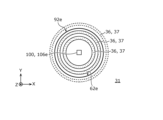
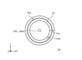
- Figure 8 shows the flat portion 37 of the chip 30 as viewed from above.
- the flat portion 37 is indicated by hatched dots.
- the position of the edge 92e of the protruding portion 92 of the mold 90 is indicated by an arrow.
- the flat portion of the chip 30 is similarly indicated in a top view.
- the flat portion 37 is located outside the exposed portion 106e on the surface 31 of the chip 30.
- the flat portion 37 is formed in a ring shape so as to surround the exposed portion 106e, similar to the protruding portion 36.
- the flat portion 37 is annular.
- the chip 30 further has a number of wires extending outward from the sensor section 100, and a number of pad electrodes located at the outer ends of the wires (not shown).
- the pad electrodes of the chip 30 are electrically connected to the pad electrodes of the substrate 20 via a number of wires 50 (see FIG. 6).
- Parts of the chip 30, the wires 50, and the substrate 20 are covered by a molded resin section 60.
- the molded resin part 60 is formed by molding a thermosetting resin.
- the molded resin part 60 is provided on the chip 30 and the substrate 20 so as not to cover the exposed portion 106e of the sensor part 100.
- the molded resin part 60 is formed so as to cover the surface 31 of the chip 30 excluding the exposed portion 106e, and the surface 21 of the substrate 20.
- FIG. 6 shows a structure in which the entire surface 21 of the substrate 20 is covered with the molded resin part 60, this is not limiting, and a structure in which a part of the substrate 20, such as the outer periphery of the substrate 20, is not covered with the molded resin may also be used.
- the molded resin part 60 has an opening hole 62 located on the exposed portion 106e.
- the opening hole 62 is an air hole that connects to the sensor part 100 from the outside and penetrates the molded resin part 60 in the thickness direction.
- one opening hole 62 is formed in the center of the molded resin part 60.
- the opening hole 62 is formed in a tapered shape so that the area of the hole increases from the inside to the outside.
- the opening hole 62 is formed by a protrusion 92 that protrudes to the inside of the mold 90 (see FIG. 2).
- the edge 62e of the opening hole 62 is circular.
- the edge 62e of the opening hole 62 on the surface 31 side of the chip 30 is located on the protrusion 36 of the insulating film 35.
- the edge 92e of the protruding part 92 of the mold 90 is pressed against the flat part 37 of the chip 30 during resin molding. Therefore, the sensor package 10 after molding has a structure in which the edge 62e of the opening hole 62 is in contact with the flat part 37 of the protruding part 36 and is formed along the flat part 37 that is flat in the circumferential direction. In other words, the edge 62e of the opening hole 62 is positioned on the same plane on the surface 31 side of the chip 30.
- a gap is less likely to form between the protruding part 92 of the mold 90 and the flat part 37 of the chip 30. This makes it possible to prevent the resin material used to form the molded resin part 60 from penetrating toward the sensor part 100. This makes it possible to prevent the quality of the sensor part 100 from deteriorating.
- the intrusion of the resin material can be suppressed, so the pressing force of the mold 90 against the chip 30 can be reduced, and the occurrence of cracks in the chip 30 can be suppressed.
- the intrusion of the resin material can be suppressed, the size of the opening hole 62 and the size of the chip 30 can be reduced.
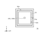
- the shape of the flat portion 37 of the tip 30 is annular, but the shape of the flat portion 37 is not limited to this.
- FIG. 9 shows another example of the flat portion 37 of the chip 30.
- the flat portion 37 of the chip 30 may be a rectangular ring.
- the rectangular shape is a square or rectangular shape.
- the protruding portion 36 of the insulating film 35 for forming the flat portion 37 and the dummy electrode 34 for forming the protruding portion 36 are also rectangular rings.
- the protruding portion 92 of the mold 90 be a truncated pyramid or prism shape, and that the edge 62e of the opening hole 62 be a square shape.
- FIG. 10 is a diagram showing a cross section of the sensor portion 100 of the sensor package 10.
- the sensor unit 100 is a fine structure that can be manufactured during the semiconductor manufacturing process, and is a wide-range hydrogen sensor that detects low and high concentrations of hydrogen. Its main components include a first electrode 103 and a second electrode 106 arranged with their principal surfaces facing each other, a metal oxide layer 104 arranged in contact with the principal surface of the first electrode 103 and the principal surface of the second electrode 106, insulating films 107a-107c, 109a and 109b covering the first electrode 103, the second electrode 106 and the metal oxide layer 104, a first terminal TE1 and a second terminal TE2 connected via a via to the other surface opposite the principal surface of the second electrode 106, and a third terminal BE connected via a via to the other surface opposite the principal surface of the first electrode 103.
- the insulating film 107b has an opening 106a that exposes the other surface of the second electrode 106 without being covered by the insulating film 107b between the first terminal TE1 and the second terminal TE2 in a plan view of the second electrode 106.
- the first electrode 103 is a planar electrode having two surfaces. One of the two surfaces of the first electrode 103 (i.e., the upper surface in FIG. 10) is in contact with the metal oxide layer 104, and the other surface (i.e., the lower surface in FIG. 10) is in contact with the insulating film 107a and the via 108. When viewed from a direction perpendicular to the main surface, the first electrode 103 is rectangular and has the same size as the second electrode 106.
- the first electrode 103 may be made of a material having a lower standard electrode potential than the metal constituting the metal oxide, such as tungsten, nickel, tantalum, titanium, aluminum, tantalum nitride, or titanium nitride.
- the first electrode 103 in FIG. 10 is made of, for example, a transition metal nitride such as tantalum nitride (TaN) or titanium nitride (TiN), or a laminate of these.
- the metal oxide layer 104 is sandwiched between the two opposing main surfaces of the first electrode 103 and the second electrode 106, and is composed of a metal oxide as a resistive film having gas sensitivity, and has a resistance value that changes reversibly depending on the presence or absence of hydrogen in the gas with which the second electrode 106 is in contact.
- the metal oxide layer 104 only needs to have the property that its resistance changes depending on the presence of hydrogen.
- the metal oxide layer 104 is composed of an oxygen-deficient metal oxide.
- the base metal of the metal oxide layer 104 may be at least one selected from transition metals such as tantalum (Ta), hafnium (Hf), titanium (Ti), zirconium (Zr), niobium (Nb), tungsten (W), nickel (Ni), and iron (Fe), and aluminum (Al).
- transition metals such as tantalum (Ta), hafnium (Hf), titanium (Ti), zirconium (Zr), niobium (Nb), tungsten (W), nickel (Ni), and iron (Fe), and aluminum (Al).
- the "oxygen deficiency" of a metal oxide refers to the ratio of the oxygen deficiency in the metal oxide to the amount of oxygen in an oxide of stoichiometric composition composed of the same elements as the metal oxide.
- the oxygen deficiency is the value obtained by subtracting the amount of oxygen in the metal oxide from the amount of oxygen in the metal oxide of stoichiometric composition. If there are multiple metal oxides of stoichiometric composition composed of the same elements as the metal oxide, the oxygen deficiency of the metal oxide is defined based on the one with the highest resistance value among those metal oxides of stoichiometric composition. Metal oxides of stoichiometric composition are more stable and have higher resistance values than metal oxides of other compositions.
- the oxide of the stoichiometric composition according to the above definition is Ta 2 O 5 , and can be expressed as TaO 2.5 .
- the oxygen deficiency of a metal oxide with excess oxygen is a negative value.
- the oxygen deficiency can be a positive value, 0, or a negative value.
- An oxide with a small oxygen deficiency is closer to an oxide of the stoichiometric composition, and therefore has a high resistance value, and an oxide with a large oxygen deficiency is closer to the metal constituting the oxide, and therefore has a low resistance value.
- the metal oxide layer 104 shown in Fig. 10 has a first layer 104a in contact with the first electrode 103, a second layer 104b in contact with the first layer 104a and the second electrode 106, and an insulating separation layer 104i.
- the second layer 104b has a smaller degree of oxygen deficiency than the first layer 104a.
- the first layer 104a is TaOx.
- the second layer 104b is Ta2O5 , which has a smaller degree of oxygen deficiency than the first layer 104a.
- the metal oxide layer 104 also has an insulating separation layer 104i on the outer periphery of the first electrode 103 in a plan view.
- a planar view refers to viewing the sensor unit 100 according to the present disclosure from a viewpoint in the stacking direction of FIG. 10, in other words, viewing from a viewpoint in the normal direction of any of the surfaces of the planar first electrode 103, the planar second electrode 106, etc., for example, viewing the top surface of the sensor unit 100 from a direction perpendicular to the main surface.
- the resistance state of the metal oxide layer 104 decreases according to the amount (the greater the amount) of hydrogen-containing gas in contact with the second electrode 106. More specifically, when hydrogen-containing gas is present in the gas to be detected, hydrogen atoms are dissociated from the hydrogen-containing gas at the second electrode 106. The dissociated hydrogen atoms penetrate the metal oxide layer 104 and form an impurity level. In particular, they are concentrated near the interface with the second electrode 106, making the second layer 104b appear thinner. As a result, the resistance value of the metal oxide layer 104 decreases.
- the second electrode 106 is a planar electrode having hydrogen dissociation properties and has two surfaces. One of the two surfaces of the second electrode 106 (i.e., the lower surface in FIG. 10) is in contact with the metal oxide layer 104, and the other surface (i.e., the upper surface in FIG. 10) is in contact with the metal layer 106s and the outside air.
- the second electrode 106 has an exposed portion 106e exposed to the outside air in the opening 106a.
- the second electrode 106 is made of a material having a catalytic effect of dissociating hydrogen atoms from gas molecules having hydrogen atoms, such as a precious metal such as platinum (Pt), iridium (Ir), or palladium (Pd), or nickel (Ni), or an alloy containing at least one of these.
- the second electrode 106 in FIG. 10 is platinum (Pt).
- Two terminals, namely, a first terminal TE1 and a second terminal TE2 are connected to the second electrode 106.
- the first terminal TE1 is connected to the second electrode 106 through a via 108.
- the second terminal TE2 is connected to the second electrode 106 through the via 108.
- the first terminal TE1 and the second terminal TE2 are connected to an external detection circuit that drives the sensor unit 100 through the openings TE1a and TE2a.
- the first terminal TE1 and the second terminal TE2 are disposed at positions sandwiching the exposed portion 106e in a plan view of the second electrode 106.
- a predetermined voltage is applied between the first terminal TE1 and the second terminal TE2
- electricity is passed through the exposed portion 106e of the second electrode 106, that is, a current is passed through the exposed portion 106e.
- This passing of electricity through the exposed portion 106e of the second electrode 106 is thought to activate the hydrogen dissociation action of the exposed portion 106e.
- the predetermined voltages may be voltages having opposite polarities.
- sensor unit 100 When gas molecules containing hydrogen atoms come into contact with exposed portion 106e while current is flowing through exposed portion 106e, sensor unit 100 changes the resistance between first terminal TE1 and second terminal TE2. The detection circuit detects this change in resistance (this detection is also called "horizontal mode"), thereby detecting gas molecules containing a low concentration of hydrogen atoms.
- the third terminal BE is connected to the first electrode 103 via the opening BEa, the via 108, the wiring 114, and the via 108.
- the third terminal BE is connected to an external detection circuit that drives the sensor unit 100 via the opening BEa.
- the sensor unit 100 changes the resistance between the first electrode 103 and the second electrode 106 when gas molecules containing hydrogen atoms touch the exposed portion 106e while a current is passing through the exposed portion 106e.
- the sensor unit 100 changes the resistance value between the third terminal BE and at least one of the first terminal TE1 and the second terminal TE2 when gas molecules containing hydrogen atoms touch the exposed portion 106e while a current is passing through the exposed portion 106e.
- the detection circuit detects this change in resistance (this detection is also called "vertical mode”), thereby detecting gas molecules containing a high concentration of hydrogen atoms.
- Insulating film 102, insulating films 107a to 107c, and insulating films 109a and 109b, which cover the main parts of sensor unit 100, are made of silicon oxide film, silicon nitride film, etc.
- a metal layer 106s is formed on the upper surface of the second electrode 106 other than the opening 106a.
- the metal layer 106s is made of, for example, TiAlN and is formed as an etching stopper for forming the via 108, but this is not essential.
- the laminate of the first electrode 103, the metal oxide layer 104, and the second electrode 106 is an element that can be used as a memory element of a resistance change memory (ReRAM).
- ReRAM resistance change memory
- two of the possible states of the metal oxide layer 104, a high resistance state and a low resistance state, are used to form a digital memory element.
- the high resistance state of the possible states of the metal oxide layer 104 is used.
- FIG. 10 an example of a two-layer structure of the metal oxide layer 104 is shown, which is composed of the first layer 104a made of TaOx and the second layer 104b made of Ta2O5 having a small oxygen deficiency, but it may be a single-layer structure made of Ta2O5 or TaOx having a small oxygen deficiency.
- FIG. 10 shows a schematic diagram in which the openings TE1a, TE2a, and BEa are located near the exposed portion 106e, this is not limiting.
- the openings TE1a, TE2a, and BEa may be located far away from the exposed portion 106e and outside the edge 62e of the opening hole 62.
- the openings TE1a, TE2a, and BEa may be located on the outer periphery of the chip 30 as openings in the pad electrode portion.
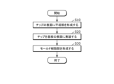
- FIG. 11 is a flowchart showing a method for manufacturing the sensor package 10.
- the method for manufacturing the sensor package 10 shown in FIG. 11 includes step S10 of forming a flat portion 37 on the surface 31 of the chip 30, step S20 of mounting the chip 30 on the surface 21 of the substrate 20, and step S30 of forming a molded resin portion 60.
- a flat portion 37 is provided outside the area where the exposed portion 106e of the sensor unit 100 is to be formed.
- the flat portion 37 may be provided on the chip 30 before the exposed portion 106e is formed, or may be provided on the chip 30 after the exposed portion 106e is formed.
- step S20 the chip 30 is mounted on the substrate 20 by wire bonding. This electrically connects the chip 30 and the substrate 20 via the wires 50.
- step S30 the protruding portion 92 of the mold 90 is placed above the exposed portion 106e of the sensor portion 100 of the chip 30, and the molded resin portion 60 is formed to cover the surface 31 of the chip 30 excluding the exposed portion 106e, and the surface 21 of the substrate 20.
- the mold 90 is placed so that the edge 92e of the protruding portion 92 is positioned on the flat portion 37, and the resin is molded.
- a film-like resin sheet may be placed along the inner surface of the mold 90 to form the molded resin portion 60.
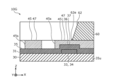
- the sensor package 10A of the first modification includes a substrate 20, a chip 30 mounted on the substrate 20, and a molded resin part 60 provided on the chip 30 and on the substrate 20.
- the configurations of the substrate 20 and the molded resin part 60 are the same as those of the first embodiment.
- FIG. 12 is a diagram showing a cross section of the chip 30 and molded resin part 60 of the sensor package 10A according to the first modified example.
- the chip 30 has multiple wirings and multiple insulating films.
- the dummy electrode 34 has a predetermined thickness and is formed in a ring shape on the outside of the exposed portion 106e.
- a lower insulating film 35u is formed on the dummy electrode 34, and a top insulating film 35 is formed on the lower insulating film 35u.
- the lower insulating film 35u is provided on the chip 30 so as to cover the dummy electrode 34 having a predetermined thickness. Therefore, a convex portion is formed on the lower insulating film 35u so as to correspond to the position where the dummy electrode 34 is provided.
- the top insulating film 35 is provided on the surface 31 of the chip 30 so as to cover the convex portion of the lower insulating film 35u. Therefore, a convex portion 36 is formed on the top insulating film 35 so as to correspond to the position where the dummy electrode 34 and the convex portion of the lower insulating film 35u are provided.
- the insulating film 35 has a convex portion 36 that protrudes in a direction perpendicular to the surface 31 of the chip 30, and the convex portion 36 is formed by the insulating film 35 that covers the upper part of the dummy electrode 34.
- This convex portion 36 is formed in a ring shape so as to surround the exposed portion 106e, following the shape of the dummy electrode 34.
- the edge 62e of the opening hole 62 is in contact with the flat portion 37 of the protrusion 36 and is formed along the flat portion 37 that is flat in the circumferential direction.
- the edge 62e of the opening hole 62 is located on the same plane on the surface 31 side of the chip 30.
- the sensor package 10B of the second modification includes a substrate 20, a chip 30 mounted on the substrate 20, and a molded resin portion 60 provided on the chip 30 and on the substrate 20.
- the configuration of the substrate 20 is the same as that of the first embodiment.
- FIG. 13 is a diagram showing a cross section of the chip 30 and molded resin part 60 of the sensor package 10B according to the second modification.
- the chip 30 has multiple wirings and multiple insulating films.
- the top layer wirings 33 are composed of multiple dummy electrodes 34.
- the dummy electrodes 34 have a predetermined thickness and are formed in a ring shape on the outside of the exposed portion 106e.
- the multiple dummy electrodes 34 are composed of two or more ring-shaped dummy electrodes 34.
- the insulating film 35 is provided on the surface 31 of the chip 30 so as to cover the multiple dummy electrodes 34. Therefore, multiple protrusions 36 are formed on the insulating film 35 so as to correspond to the positions where the multiple dummy electrodes 34 are provided.
- the insulating film 35 has multiple protrusions 36 that protrude in a direction perpendicular to the surface 31 of the chip 30, and the multiple protrusions 36 are formed by the insulating film 35 covering the upper parts of the dummy electrodes 34.
- the multiple protrusions 36 are formed in two or more rings so as to surround the exposed portion 106e according to the shape of the dummy electrode 34. Annular recesses (opening grooves) are formed between the multiple protrusions 36.
- the tip of the annular convex portion 36 is provided with a flat portion 37, which is a flat region.
- the flat portions 37 formed corresponding to the multiple convex portions 36 are formed on the same plane.
- the difference in height between the flat portions 37 formed on the multiple convex portions 36 is less than 1 ⁇ m.
- the convex portion 36 is formed by covering only the dummy electrode 34 with the insulating film 35, but this is not limited to this.
- the convex portion 36 may be formed by covering wiring that combines a dummy electrode and wiring for electrical connection with the insulating film 35.
- FIG. 14 shows the flat portion 37 of the chip 30 of the second modified example as viewed from above.
- the flat portions 37 are composed of two or more annular flat portions 37. Each flat portion 37 is located outside the exposed portion 106e on the surface 31 of the chip 30. Each flat portion 37, like each protrusion 36, is formed in an annular shape so as to surround the exposed portion 106e.
- the molded resin part 60 has an opening hole 62 located on the exposed portion 106e.
- the opening hole 62 is an air hole that connects to the sensor part 100 from the outside, and penetrates the molded resin part 60 in the thickness direction.
- the opening hole 62 is formed by a protrusion 92 that protrudes inward from the mold 90. For example, if the shape of the protrusion 92 is a truncated cone or a cylinder, the edge 62e of the opening hole 62 will be circular.
- the sensor package 10B after molding has a structure in which the edge 62e of the opening hole 62 is located between the outermost convex part 36 and the second convex part 36 counting from the outermost.
- the edge 62e of the opening hole 62 is formed along each of the flat part 37 of the outermost convex part 36 and the flat part 37 of the second convex part 36.
- the height of the edge 62e is the same as the height of these flat parts 37.
- the chip 30 has one or more annular flat parts 37, when forming the molded resin part 60, the bottom surface of the protruding part 92 and the flat part 37 come into contact with each other, and it is possible to prevent the resin material from leaking toward the sensor part 100. This makes it possible to prevent the quality of the sensor part 100 from deteriorating.
- annular pattern two or more layers, even if the resin infiltrates beyond the outer annular pattern, the resin that has infiltrated into the annular recess (opening groove) between the multiple protruding parts 36 can be trapped. Therefore, it is possible to reduce the risk that the sensor part 100 will be covered with resin beyond the innermost annular pattern.
- the shape of the flat portion 37 of the tip 30 is annular, but the shape of the flat portion 37 is not limited to this.
- FIG. 15 shows another example of the flat portion 37 of the chip 30.
- the flat portion 37 of the chip 30 may be a rectangular ring.
- the rectangular shape is a square or rectangular shape.
- the protruding portion 36 of the insulating film 35 for forming the flat portion 37 and the dummy electrode 34 for forming the protruding portion 36 are also rectangular rings.
- the protruding portion 92 of the mold 90 be a truncated pyramid or prism shape, and that the edge 62e of the opening hole 62 be a square shape.
- the sensor package 10C of the third modification includes a substrate 20, a chip 30 mounted on the substrate 20, and a molded resin part 60 provided on the chip 30 and on the substrate 20.
- the configurations of the substrate 20 and the molded resin part 60 are the same as those of the second modification.
- FIG. 16 is a diagram showing a cross section of the chip 30 and molded resin part 60 of the sensor package 10C according to the third modification.
- the chip 30 has multiple wirings and multiple insulating films.
- the dummy electrode 34 has a predetermined thickness and is formed in a ring shape on the outside of the exposed portion 106e.
- a lower insulating film 35u is formed on the dummy electrode 34, and a top insulating film 35 is formed on the lower insulating film 35u.
- the lower insulating film 35u is provided on the chip 30 so as to cover the dummy electrode 34 having a predetermined thickness. Therefore, a convex portion is formed on the lower insulating film 35u so as to correspond to the position where the dummy electrode 34 is provided.
- the top insulating film 35 is provided on the surface 31 of the chip 30 so as to cover the convex portion of the lower insulating film 35u. Therefore, a convex portion 36 is formed on the top insulating film 35 so as to correspond to the position where the dummy electrode 34 and the convex portion of the lower insulating film 35u are provided.
- the insulating film 35 has a convex portion 36 that protrudes in a direction perpendicular to the surface 31 of the chip 30, and the convex portion 36 is formed by the insulating film 35 that covers the upper part of the dummy electrode 34.
- This convex portion 36 is formed in a ring shape so as to surround the exposed portion 106e, following the shape of the dummy electrode 34.
- the bottom surface of the protrusion 92 of the mold 90 is pressed against the inner flat portion 37 during resin molding.
- the edge 62e of the opening hole 62 is located on the same plane as the surface 31 of the chip 30. This structure achieves the same effect as the first embodiment.
- the chip 30 has one or more annular flat portions 37, so that when the molded resin portion 60 is formed, the bottom surface of the protrusion 92 comes into contact with the flat portion 37, preventing the resin material from leaking toward the sensor portion 100. This prevents the quality of the sensor portion 100 from deteriorating. Furthermore, by making the annular pattern two or more times, even if the resin penetrates beyond the outer annular pattern, the resin that penetrates into the annular recesses (opening grooves) between the multiple protrusions 36 can be trapped. This reduces the risk that the sensor portion 100 will be covered with resin beyond the innermost annular pattern.
- a sensor package 10D according to a fourth modification of the first embodiment will be described.
- the fourth modification an example will be described in which the chip 30 has two or more annular flat portions 37 and an opening groove 38 is provided in the insulating film 35 of the chip 30.
- the sensor package 10D of the fourth modification includes a substrate 20, a chip 30 mounted on the substrate 20, and a molded resin portion 60 provided on the chip 30 and on the substrate 20.
- the configuration of the substrate 20 is the same as that of the third modification.
- FIG. 17 is a diagram showing a cross section of the chip 30 and molded resin part 60 of the sensor package 10D relating to the fourth modification example.
- the chip 30 has a plurality of insulating films.
- the top insulating film 35 is formed on the planarized lower insulating film 35u.
- the top insulating film 35 has a flat portion 37, which is a flat region, and a plurality of opening grooves 38 recessed relative to the flat portion 37.
- the opening grooves 38 penetrate the top insulating film 35 in the thickness direction and are formed so as to expose the lower insulating film 35u.
- the plurality of opening grooves 38 are composed of two or more annular opening grooves 38.
- the annular opening grooves 38 are formed in the insulating film 35, dividing the flat portion 37 into an inner portion and an outer portion.
- the divided plurality of flat portions 37 are formed in an annular shape so as to surround the exposed portion 106e along the shape of the opening groove 38.
- the opening groove 38 is annular, and the plurality of flat portions 37 are composed of two or more annular flat portions 37.
- Each flat portion 37 is formed on the same plane, and the difference in height between each flat portion 37 is, for example, less than 1 ⁇ m.
- the opening groove 38 penetrates the insulating film 35, but this is not limited thereto.
- the opening groove 38 may be an annular recess (annular groove) that leaves the bottom of the insulating film 35.
- the molded resin part 60 has an opening hole 62 located on the exposed portion 106e.
- the opening hole 62 is an air hole that connects to the sensor part 100 from the outside, and penetrates the molded resin part 60 in the thickness direction.
- the opening hole 62 is formed by a protrusion 92 that protrudes inward from the mold 90. For example, if the shape of the protrusion 92 is a truncated cone or a cylinder, the edge 62e of the opening hole 62 will be circular.
- the sensor package 10D after molding has a structure in which the edge 62e of the opening hole 62 is in contact with the outermost flat portion 37 and is formed along the outermost flat portion 37.
- the edge 62e of the opening hole 62 is located on the same plane on the surface 31 side of the chip 30.
- a gap is less likely to be formed between the protruding part 92 of the mold 90 and the flat part 37 of the chip 30.
- the chip 30 has one or more annular flat parts 37, when forming the molded resin part 60, the bottom surface of the protruding part 92 and the flat part 37 come into contact with each other, and the resin material is prevented from leaking toward the sensor part 100. This prevents the quality of the sensor part 100 from deteriorating.
- the annular pattern two or more layers, even if the resin penetrates beyond the outer annular pattern, the resin that penetrates into the annular recesses (opening grooves) between the multiple protruding parts 36 can be trapped. Therefore, the risk of the sensor part 100 being covered with resin beyond the innermost annular pattern can be reduced.
- the shape of the flat portion 37 of the tip 30 was annular, but the shape of the flat portion 37 may be circular or rectangular.
- the outermost flat portion 37 that contacts the edge 92e of the protruding portion 92 of the mold 90 does not necessarily have to be annular, and may have a recess formed partially.
- the sensor package 10E of the fifth modification includes a substrate 20, a chip 30 mounted on the substrate 20, and a molded resin part 60 provided on the chip 30 and on the substrate 20.
- the configurations of the substrate 20 and the molded resin part 60 are the same as those of the fourth modification.
- FIG. 18 is a diagram showing a cross section of the chip 30 and molded resin part 60 of the sensor package 10E relating to the fifth modification example.
- the chip 30 has multiple wirings and multiple insulating films.
- the dummy electrode 34 has a predetermined thickness and is formed in a ring shape on the outside of the exposed portion 106e.
- a lower insulating film 35u is formed on the dummy electrode 34, and a top insulating film 35 is formed on the lower insulating film 35u.
- the lower insulating film 35u is provided on the chip 30 so as to cover the dummy electrode 34 having a predetermined thickness. Therefore, a convex portion is formed on the lower insulating film 35u so as to correspond to the position where the dummy electrode 34 is provided.
- the top insulating film 35 is provided on the surface 31 of the chip 30 so as to cover the convex portion of the lower insulating film 35u. Therefore, a convex portion 36 is formed on the top insulating film 35 so as to correspond to the position where the dummy electrode 34 and the convex portion of the lower insulating film 35u are provided.
- the insulating film 35 has a convex portion 36 that protrudes in a direction perpendicular to the surface 31 of the chip 30, and the convex portion 36 is formed by the insulating film 35 that covers the upper part of the dummy electrode 34.
- This convex portion 36 is formed in a ring shape so as to surround the exposed portion 106e, following the shape of the dummy electrode 34.
- the tip of the convex portion 36 forms a flat portion 37.
- the insulating film 35 of the fifth modified example has a flat portion 37 at the tip of the protrusion 36, and a plurality of opening grooves 38 recessed relative to the flat portion 37.
- the plurality of opening grooves 38 are configured by two or more annular opening grooves 38.
- the annular opening grooves 38 are formed in the insulating film 35, dividing the flat portion 37 into an inner portion and an outer portion.
- the divided plurality of flat portions 37 are formed in an annular shape so as to surround the exposed portion 106e according to the shape of the opening groove 38.
- the opening groove 38 in this example is annular, and the plurality of flat portions 37 are configured by two or more annular flat portions 37.
- Each flat portion 37 is formed on the same plane, and the difference in height between each flat portion 37 is, for example, less than 1 ⁇ m.
- the molded resin part 60 has an opening hole 62 located on the exposed portion 106e.
- the opening hole 62 is an air hole that connects to the sensor part 100 from the outside, and penetrates the molded resin part 60 in the thickness direction.
- the opening hole 62 is formed by a protrusion 92 that protrudes inward from the mold 90. For example, if the shape of the protrusion 92 is a truncated cone or a cylinder, the edge 62e of the opening hole 62 will be circular.
- the sensor package 10E after molding has a structure in which the edge 62e of the opening hole 62 is in contact with the outermost flat portion 37 and is formed along the outermost flat portion 37.
- the edge 62e of the opening hole 62 is located on the same plane on the surface 31 side of the chip 30.
- a gap is less likely to form between the protrusion 92 of the mold 90 and the flat portion 37 of the chip 30. This makes it possible to prevent the resin material used to form the molded resin portion 60 from penetrating toward the sensor portion 100.
- the chip 30 has two or more annular flat portions 37, it is possible to prevent the resin material from leaking toward the sensor portion 100. This makes it possible to prevent a deterioration in the quality of the sensor portion 100.
- the shape of the flat portion 37 of the chip 30 was annular, but the shape of the flat portion 37 may be circular or angular.
- the outermost flat portion 37 that contacts the edge 92e of the protrusion 92 of the mold 90 does not necessarily have to be annular, and may have a partial recess formed therein.
- the pattern below the outermost flat portion 37 that contacts the edge 92e of the protrusion 92 does not necessarily have to be annular, and may be wiring for electrical connection or an island-shaped dummy pattern, etc.
- the protrusion 36 is formed by covering only the dummy electrode 34 with the insulating film 35, but this is not limiting.
- the protrusion 36 may be formed by covering a wiring that combines a dummy electrode and a wiring for electrical connection with the insulating film 35.
- a sensor package 10F according to a sixth modification of the first embodiment will be described.
- a protective film 45 is formed on an insulating film 35 will be described.
- the sensor package 10F of the sixth modification includes a substrate 20, a chip 30 mounted on the substrate 20, and a molded resin portion 60 provided on the chip 30 and on the substrate 20.
- the configuration of the substrate 20 is the same as that of the first embodiment.
- FIG. 19 is a diagram showing a cross section of the chip 30 and molded resin part 60 of a sensor package 10F relating to modification example 6.
- a protective film 45 is formed to cover the protruding portion 36 of the insulating film 35.
- the protective film 45 is formed, for example, from a polyimide resin or a fluororesin.
- the protective film 45 is provided on the surface 31 of the chip 30 so as to cover the protruding portion 36 of the insulating film 35 and not cover the exposed portion 106e of the sensor portion 100.
- the inner side surface 45s of the protective film 45 is located slightly closer to the exposed portion 106e than the protruding portion 36, and is located closer to the edge 62e of the opening hole 62 than the exposed portion 106e.
- the protective film 45 on the protrusion 36 has a flat area, that is, a flat portion 47.
- the flat portion 47 is continuously flat in the circumferential direction surrounding the exposed portion 106e, without any steps.
- the difference in height between the protrusions and recesses of the flat portion 47 is less than 1 ⁇ m.
- the flat area of the protective film 45 only needs to be formed in correspondence with the area where the protrusion 92 of the mold 90 comes into contact. For example, an area a little away from the edge 92e of the protrusion 92 to the outside does not necessarily need to be flat, and the protective film itself does not need to be formed.
- FIG. 20 shows the flat portion 47 of the chip 30 of variant 6 as viewed from above.
- the flat portion 47 is located outside the exposed portion 106e on the surface 31 of the chip 30.
- the flat portion 47 is formed to surround the exposed portion 106e, similar to the protruding portion 36.
- the inner circumference (inner side surface 45s) of the flat portion 47 is circular.
- the molded resin part 60 has an opening 62 located on the exposed portion 106e.
- the opening 62 is an air hole that connects to the sensor part 100 from the outside, and penetrates the molded resin part 60 in the thickness direction.
- the opening 62 is formed by a protrusion 92 that protrudes inward from the mold 90.
- the edge 62e of the opening 62 is circular.
- the edge 62e of the opening 62 is located on the protective film 45 above the convex part 36.
- the sensor package 10F after molding has a structure in which the edge 62e of the opening hole 62 is in contact with the flat part 47 of the protective film 45 and is formed along the flat part 47 of the protective film 45.
- the edge 62e of the opening hole 62 is located on the same plane on the surface 31 side of the chip 30.
- a gap is less likely to form between the protruding part 92 of the mold 90 and the flat part 47 of the chip 30. This makes it possible to prevent the resin material used to form the molded resin part 60 from penetrating toward the sensor part 100. This makes it possible to prevent the quality of the sensor part 100 from deteriorating.
- the resin material for forming the molded resin portion 60 penetrates between the protective film 45 and the protruding portion 92, the resin material can be guided circumferentially along the inner peripheral end of the protruding portion 92 by surface tension, and the penetration of the resin material can be stopped at the inner peripheral end of the protective film 45. This makes it possible to prevent the quality of the sensor portion 100 from deteriorating.
- the inner circumference of the flat portion 47 of the tip 30 is circular, but the shape of the flat portion 47 is not limited to this.
- the inner circumference of the flat portion 47 of the tip 30 may be angular.
- the protrusion 36 is formed by a ring-shaped dummy electrode 34 below the flat portion 47 of the protective film 45, but this is not limiting.
- the dummy electrode 34 for forming the protrusion 36 may be absent, or may be a non-ring-shaped pattern (such as wiring for electrical connection or an island-shaped dummy pattern).
- the sensor package 10G of the seventh modification includes a substrate 20, a chip 30 mounted on the substrate 20, and a molded resin part 60 provided on the chip 30 and on the substrate 20.
- the configurations of the substrate 20 and the molded resin part 60 are the same as those of the sixth modification.
- FIG. 21 is a diagram showing a cross section of the chip 30 and molded resin part 60 of a sensor package 10G relating to modification example 7.
- the protective film 45 is formed in two or more layers in a ring shape. A part of the protective film 45 is formed so as to cover the convex portion 36 of the insulating film 35, and the remaining part is formed at a distance inward from the protective film 45 that covers the convex portion 36.
- Each of these protective films 45 has a flat area 47.
- the flat area 47 is continuously flat in the circumferential direction surrounding the exposed portion 106e without any steps.
- FIG. 22 shows the flat portion 47 of the chip 30 of variant 7 as viewed from above.
- the flat portion 47 is located outside the exposed portion 106e on the surface 31 of the chip 30.
- the flat portion 47 of the protective film 45 is formed to surround the exposed portion 106e.
- the inner circumference (inner side surface 45s) of each flat portion 47 is circular.
- the molded resin part 60 has an opening hole 62 located on the exposed portion 106e.
- the opening hole 62 is an air hole that connects to the sensor part 100 from the outside, and penetrates the molded resin part 60 in the thickness direction.
- the opening hole 62 is formed by a protrusion 92 that protrudes inward from the mold 90. For example, if the shape of the protrusion 92 is a truncated cone or a cylinder, the edge 62e of the opening hole 62 will be circular.
- the sensor package 10G after molding has a structure in which the edge 62e of the opening hole 62 is in contact with the flat portion 47 of the protective film 45 and is formed along the flat portion 47 of the protective film 45.
- the edge 62e of the opening hole 62 is located on the same plane on the surface 31 side of the chip 30.
- the chip 30 has one or more annular flat parts 37, when forming the molded resin part 60, the bottom surface of the protruding part 92 and the flat part 37 come into contact with each other, and the resin material is prevented from leaking toward the sensor part 100. This prevents the quality of the sensor part 100 from deteriorating. Furthermore, by making the annular pattern two or more layers, even if the resin penetrates beyond the outer annular pattern, the resin that penetrates into the annular recesses (opening grooves) between the multiple protruding parts 36 can be trapped. Therefore, the risk of the sensor part 100 being covered with resin beyond the innermost annular pattern can be reduced.
- the inner circumference of the flat portion 47 of the tip 30 is circular, but the shape of the flat portion 47 is not limited to this.
- the inner circumference of the flat portion 37 of the tip 30 may be angular.
- the protrusion 36 is formed by a ring-shaped dummy electrode 34 below the flat portion 47 of the protective film 45, but this is not limiting.
- the dummy electrode 34 for forming the protrusion 36 may be absent, or may be a non-ring-shaped pattern (such as wiring for electrical connection or an island-shaped dummy pattern).
- the sensor package 10H of the eighth modification includes a substrate 20, a chip 30 mounted on the substrate 20, and a molded resin part 60 provided on the chip 30 and on the substrate 20.
- the configurations of the substrate 20 and the molded resin part 60 are the same as those of the fourth modification.
- FIG. 23 is a diagram showing a cross section of the chip 30 and molded resin part 60 of a sensor package 10H relating to modification example 8.
- the chip 30 has a plurality of insulating films.
- the top insulating film 35 is formed on the planarized lower insulating film 35u.
- the top insulating film 35 has a flat portion 37, which is a flat region, and a guide groove 48 that is recessed relative to the flat portion 37.
- the guide groove 48 is a groove that guides the resin material that has entered between the protrusion 92 and the flat portion 37 during resin molding in a direction different from the direction of the exposed portion 106e.
- the guide groove 48 penetrates the insulating film 35 in the thickness direction and is formed so that the lower insulating film 35u is exposed.
- the guide groove 48 is single-layered, but may be formed with two or more layers.
- the shape of the guide groove 48 is spiral or snake-shaped, and the circumferential path of the guide groove 48 is lengthened, thereby increasing the amount of resin that can be trapped.
- FIG. 24 shows the guide groove 48 of the tip 30 in variant 8 of embodiment 1.
- the guide groove 48 is arc-shaped and formed along the inner side surface of the outermost flat portion 37.
- a plurality of guide grooves 48 are formed in the flat portion 37.
- One end of the arc-shaped guide groove 48 is connected to a predetermined location of the edge 62e of the opening hole 62, and the other end is connected to another location of the edge 62e of the opening hole 62. Note that it is not necessary for both ends of the guide groove 48 to be in contact with the edge 62e, and either one may be located inside the edge 62e.
- one end of the guide groove 48 may be connected to the edge 62e, and the other end may be located inside the edge 62e.
- One end of the guide groove 48 may be located inside the edge 62e, and the other end may be connected to the edge 62e. Also, it is not necessary for only one end and the other end of the guide groove 48 to be located inside the edge 62e, and both one end and the other end may be located inside the edge 62e.
- the sensor package 10H has a structure in which the edge 62e of the opening hole 62 is in contact with the outermost flat portion 37 and is formed along the outermost flat portion 37.
- a gap is less likely to form between the protruding part 92 of the mold 90 and the flat part 37 of the chip 30. This makes it possible to prevent the resin material used to form the molded resin part 60 from penetrating toward the sensor part 100. This makes it possible to prevent the quality of the sensor part 100 from deteriorating.
- the resin material for forming the molded resin portion 60 can be guided along the guide groove 48 of the flat portion 37, and the penetration of the resin material can be stopped within the guide groove 48. This makes it possible to prevent the quality of the sensor portion 100 from deteriorating.
- the guide groove 48 has an arc-shaped shape, but the shape of the guide groove 48 is not limited to this.
- FIG. 25 shows another example of the guide groove 48 of the tip 30.
- the guide groove 48 of the chip 30 may have four sides.
- the protrusion 92 of the mold 90 be in the shape of a square prism and the edge 62e of the opening hole 62 be in the shape of a square.
- a sensor package 10i according to a ninth modification of the first embodiment will be described.
- the ninth modification an example in which another insulating film is formed between the dummy electrode 34 and the protrusion 36 in the sensor package of the eighth modification will be described.
- the sensor package 10i of the ninth modification includes a substrate 20, a chip 30 mounted on the substrate 20, and a molded resin part 60 provided on the chip 30 and on the substrate 20.
- the configurations of the substrate 20 and the molded resin part 60 are the same as those of the eighth modification.
- FIG. 26 is a diagram showing a cross section of the chip 30 and molded resin part 60 of the sensor package 10i relating to variant example 9.
- the chip 30 has multiple wirings and multiple insulating films.
- the dummy electrodes 34 have a predetermined thickness and are formed in a ring shape on the outside of the exposed portion 106e.
- the figure shows an example in which the wirings 33 are formed by the dummy electrodes 34, but this is not limited to this.
- the wirings 33 may be formed by combining dummy electrodes and wiring for electrical connection.
- the wirings 33 do not need to be in a closed ring shape, and may be formed so that open areas are provided by multiple wiring patterns. By providing open areas, it is possible to provide a wiring path for electrical connection that connects the inside and outside of the edge 62e.
- a lower insulating film 35u is formed on the dummy electrode 34, and a top insulating film 35 is formed on the lower insulating film 35u.
- the lower insulating film 35u is provided on the chip 30 so as to cover the dummy electrode 34 having a predetermined thickness. Therefore, a convex portion is formed on the lower insulating film 35u so as to correspond to the position where the dummy electrode 34 is provided.
- the top insulating film 35 is provided on the surface 31 of the chip 30 so as to cover the convex portion of the lower insulating film 35u. Therefore, a convex portion 36 is formed on the top insulating film 35 so as to correspond to the position where the dummy electrode 34 and the convex portion of the lower insulating film 35u are provided.
- the insulating film 35 has a convex portion 36 that protrudes in a direction perpendicular to the surface 31 of the chip 30, and the convex portion 36 is formed by the insulating film 35 that covers the upper part of the dummy electrode 34.
- This convex portion 36 is formed in a ring shape so as to surround the exposed portion 106e, following the shape of the dummy electrode 34.
- the tip of the convex portion 36 forms a flat portion 37.
- the insulating film 35 of the ninth modification also has a flat portion 37 at the tip of the protrusion 36 and a guide groove 48 recessed relative to the flat portion 37.
- the guide groove 48 is arc-shaped and formed along the inner side surface of the outermost flat portion 37.
- a plurality of guide grooves 48 are formed in the flat portion 37.
- One end of the arc-shaped guide groove 48 is connected to a predetermined location on the edge 62e of the opening hole 62, and the other end is connected to another location on the edge 62e of the opening hole 62.
- the guide groove 48 may be formed by forming a dummy electrode 34 on the lower insulating film 35u (see FIG. 13) and covering the dummy electrode 34 and the lower insulating film 35u with the insulating film 35. In other words, the guide groove 48 may be formed by utilizing the difference in height of the insulating film 35 caused by the presence or absence of the dummy electrode 34.
- the molded resin part 60 has an opening hole 62 located on the exposed portion 106e.
- the opening hole 62 is an air hole that connects to the sensor part 100 from the outside, and penetrates the molded resin part 60 in the thickness direction.
- the opening hole 62 is formed by a protrusion 92 that protrudes inward from the mold 90. For example, if the shape of the protrusion 92 is a truncated cone or a cylinder, the edge 62e of the opening hole 62 will be circular.
- the sensor package 10i when molding the molded resin portion 60, the edge 92e of the protruding portion 92 of the mold 90 is pressed against the outermost flat portion 37. Therefore, after molding, the sensor package 10i has a structure in which the edge 62e of the opening hole 62 is in contact with the outermost flat portion 37 and is formed along the outermost flat portion 37.
- a gap is less likely to form between the protrusion 92 of the mold 90 and the flat portion 37 of the chip 30. This makes it possible to prevent the resin material used to form the molded resin portion 60 from penetrating toward the sensor portion 100.
- the chip 30 has two or more annular flat portions 37, it is possible to prevent the resin material from leaking toward the sensor portion 100. This makes it possible to prevent a deterioration in the quality of the sensor portion 100.
- the resin material for forming the molded resin portion 60 can be guided along the guide groove 48 of the flat portion 37, and the penetration of the resin material can be stopped within the guide groove 48. This makes it possible to prevent the quality of the sensor portion 100 from deteriorating.
- the guide groove 48 has an arc-shaped shape, but the shape of the guide groove 48 is not limited to this.
- the guide groove 48 of the tip 30 may have four sides.
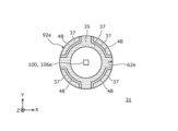
- the sensor package 10J of the tenth modification includes a substrate 20, a chip 30 mounted on the substrate 20, and a molded resin part 60 provided on the chip 30 and on the substrate 20.
- the configuration of the substrate 20 is the same as that of the first embodiment.
- FIG. 27 is a top view of the flat portion 37 of the chip 30 of the sensor package 10J relating to modification example 10.
- the flat portion 37 is located on the surface 31 of the chip 30 outside the exposed portion 106e.
- the chip 30 of variant 10 has two flat portions 37.
- Each flat portion 37 is strip-shaped when viewed from a direction perpendicular to the surface 31 of the chip 30.
- the two strip-shaped flat portions 37 are provided on both outer sides of the exposed portion 106e and are parallel to each other.
- the molded resin part 60 has an opening hole 62 located on the exposed part 106e.
- the opening hole 62 is rectangular when viewed perpendicular to the surface 31 of the chip 30.
- the length of the long side edge 62e of the opening hole 62 is formed to separate the short side from the exposed part 106e and to ensure that the resin that has entered from the short side does not reach the exposed part 106e.
- the length of the long side edge 62e is, for example, 3 to 6 times the length of the short side edge 62e.
- the two long side edges 62e of the opening hole 62 are each formed along two band-shaped flat parts 37. Note that in this example, no flat parts 37 are formed at positions corresponding to the two short sides of the opening hole 62.
- the opening hole 62 is formed by a protrusion 92 that protrudes inward from the mold 90.
- the protrusion 92 has a prism-like or truncated pyramid-like shape with long and short sides on the bottom surface.
- the resin when molding the molded resin portion 60, the resin is molded in a state in which the long side edges 92e of the protrusion 92 of the mold 90 are pressed against the two band-shaped flat portions 37. Therefore, the sensor package 10J after molding has a structure in which the long side edges 62e of the opening hole 62 are in contact with the band-shaped flat portions 37 and are formed along the band-shaped flat portions 37.
- a gap is less likely to form between the protruding part 92 of the mold 90 and the flat part 37 of the chip 30. This makes it possible to prevent the resin material used to form the molded resin part 60 from penetrating toward the sensor part 100. This makes it possible to prevent the quality of the sensor part 100 from deteriorating.
- a sensor package 10K according to an eleventh modification of the first embodiment will be described.
- the chip 30 has two pairs of double band-shaped flat portions 37.
- the sensor package 10K of the 11th modification includes a substrate 20, a chip 30 mounted on the substrate 20, and a molded resin portion 60 provided on the chip 30 and on the substrate 20.
- the configuration of the substrate 20 is the same as that of the first embodiment.
- FIG. 28 is a top view of the flat portion 37 of the chip 30 of the sensor package 10K relating to variant example 11.
- the flat portions 37 are located on the surface 31 of the chip 30 outside the exposed portion 106e.
- the chip 30 of variant 11 has two sets of double band-shaped flat portions 37.
- the two sets of double band-shaped flat portions 37 are provided on both outer sides of the exposed portion 106e and are parallel to each other.
- the molded resin part 60 has an opening hole 62 located on the exposed portion 106e.
- the opening hole 62 is rectangular when viewed from a direction perpendicular to the surface 31 of the chip 30.
- the length of the long side edge 62e of the opening hole 62 is 3 to 6 times the length of the short side edge 62e.
- Each of the two long side edges 62e of the opening hole 62 is formed along the flat portion 37 of one of the double bands. Note that in this example, the flat portion 37 is not formed at the positions corresponding to the two short sides of the opening hole 62.
- the opening hole 62 is formed by a protrusion 92 that protrudes inward from the mold 90.
- the protrusion 92 has a prism-like or truncated pyramid-like shape with long and short sides.
- the edge 92e of the long side of the protrusion 92 of the mold 90 is pressed against the band-shaped flat part 37 during resin molding. Therefore, the sensor package 10K after molding has a structure in which part of the edge 62e of the opening hole 62 is in contact with the band-shaped flat part 37 and is formed along the band-shaped flat part 37.
- a gap is less likely to form between the protruding part 92 of the mold 90 and the flat part 37 of the chip 30. This makes it possible to prevent the resin material used to form the molded resin part 60 from penetrating toward the sensor part 100. This makes it possible to prevent the quality of the sensor part 100 from deteriorating.
- the sensor package 10L of the 12th modification includes a substrate 20, a chip 30 mounted on the substrate 20, and a molded resin part 60 provided on the chip 30 and on the substrate 20.
- the configurations of the substrate 20 and the molded resin part 60 are the same as those of the first embodiment.
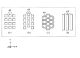
- FIG. 29 is a diagram showing a cross section of a via conductor 49 of a chip 30 of a sensor package 10L relating to modification example 12.
- the top layer wiring 33 is connected to the lower layer wiring 33u through multiple via conductors 49. This increases the strength of the lower part of the insulating film 35 that receives the pressing force from the mold 90. This structure makes it possible to suppress the formation of defects such as cracks in the chip 30. This can reduce the quality of the sensor section 100.
- Figure 30 shows a cross section of another example of a via conductor 49.
- multiple via conductors 49 may be formed in a multi-layer structure.
- Figure 31 shows a top view of the via conductor 49.
- the via conductors 49 may be arranged in a matrix as shown in FIG. 31(a), or may be arranged in a staggered pattern as shown in FIG. 31(b).
- the via conductors 49 may be formed in a honeycomb pattern as shown in FIG. 31(c), or may be formed in multiple lines as shown in FIG. 31(d).
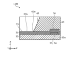
- the sensor package 10M includes a substrate 20, a chip 30 mounted on the substrate 20, and a molded resin portion 60 provided on the chip 30 and on the substrate 20.
- the configurations of the substrate 20 and the chip 30 are the same as those in the first embodiment.
- Figure 32 shows a cross section of the chip 30 and molded resin part 60 of the sensor package 10M.
- the chip 30 has multiple wirings and multiple insulating films.
- the top layer wirings 33 are formed on the planarized lower layer insulating film 35u.
- a part of the top layer wirings 33 is composed of a dummy electrode 34 that is not electrically connected to the sensor unit 100.
- the dummy electrode 34 has a predetermined thickness and is formed in a ring shape outside the exposed portion 106e. In this example, the dummy electrode 34 is ring-shaped.
- a top-layer insulating film 35 is formed on the lower-layer insulating film 35u and the top-layer wiring 33.
- the insulating film formed on the surface 31 of the chip 30 serves as the top-layer insulating film 35.
- the material of the top-layer insulating film 35 is, for example, silicon nitride.
- the insulating film 35 is provided on the surface 31 of the chip 30 so as to cover the dummy electrode 34, which has a predetermined thickness. Therefore, a convex portion 36 is formed on the insulating film 35 so as to correspond to the position where the dummy electrode 34 is provided.
- the insulating film 35 has a convex portion 36 that protrudes in a direction perpendicular to the surface 31 of the chip 30, and the convex portion 36 is formed by the insulating film 35 covering the upper part of the dummy electrode 34.
- This convex portion 36 is formed in a ring shape so as to surround the exposed portion 106e, following the shape of the dummy electrode 34.
- a flat portion 37a is provided inside the annular convex portion 36.
- the flat portion 37a is formed to be flat by not placing upper or lower layer wiring that would cause a step below the flat portion 37a.
- the flat portion 37a inside the convex portion 36 is formed continuously flat without steps in the circumferential direction surrounding the exposed portion 106e.
- the difference in height between the concaves and convexes of the flat portion 37a is less than 1 ⁇ m.
- Figure 33 shows the flat portion 37a of the chip 30 of the sensor package 10M as viewed from above.
- the flat portion 37a is located outside the exposed portion 106e on the surface 31 of the chip 30.
- the flat portion 37a is formed in a ring shape so as to surround the exposed portion 106e.
- the flat portion 37a is annular.
- the molded resin part 60 is formed by molding a thermosetting resin.
- the molded resin part 60 is provided on the chip 30 and the substrate 20 so as not to cover the exposed portion 106e of the sensor part 100.
- the molded resin part 60 is formed so as to cover the surface 31 of the chip 30 excluding the exposed portion 106e, and the surface 21 of the substrate 20.
- the molded resin part 60 has an opening hole 62 located on the exposed portion 106e.
- the opening hole 62 is an air hole that connects to the sensor part 100 from the outside, and penetrates the molded resin part 60 in the thickness direction.
- one opening hole 62 is formed in the center of the molded resin part 60.
- the opening hole 62 is formed in a tapered shape so that the area of the hole increases from the inside to the outside.
- the opening hole 62 is formed by a protrusion 92 that protrudes inward from the mold 90. For example, if the shape of the protrusion 92 is a truncated cone or a cylinder, the edge 62e of the opening hole 62 will be circular.
- the sensor package 10M after molding has a structure in which the edge 62e of the opening hole 62 on the surface 31 side of the chip 30 is in contact with the flat part 37a of the insulating film 35 and is formed along the flat part 37a that is flat in the circumferential direction.
- the edge 62e of the opening hole 62 is located on the same plane on the surface 31 side of the chip 30.
- a gap is less likely to form between the protruding portion 92 of the mold 90 and the flat portion 37a of the chip 30. This makes it possible to prevent the resin material used to form the molded resin portion 60 from penetrating toward the sensor portion 100. This makes it possible to prevent the quality of the sensor portion 100 from deteriorating.
- the intrusion of the resin material can be suppressed, so the pressing force of the mold 90 against the chip 30 can be reduced, and the occurrence of cracks in the chip 30 can be suppressed.
- the intrusion of the resin material can be suppressed, the size of the opening hole 62 and the size of the chip 30 can be reduced.
- the shape of the flat portion 37a of the tip 30 is annular, but the shape of the flat portion 37a is not limited to this.
- FIG. 34 shows another example of the flat portion 37a of the chip 30.
- the flat portion 37a of the chip 30 may be in a rectangular shape.
- the rectangular shape is a square or rectangular shape.
- the protrusion 36 of the insulating film 35 and the dummy electrode 34 for forming the protrusion 36 are also in a rectangular shape.
- the protrusion 92 of the mold 90 be in a truncated pyramid or prism shape, and that the edge 62e of the opening hole 62 be in a rectangular shape.
- the dummy electrode 34 and the protrusion 36 are formed in a ring shape, but this is not limited thereto.
- the dummy electrode 34 and the protrusion 36 may be arranged in an island shape, scattered at multiple locations, as long as they are outside the flat portion 37a.
- the protrusion 36 is formed by covering only the dummy electrode 34 with the insulating film 35, but this is not limited thereto.
- the protrusion 36 may be formed by covering a wiring that combines a dummy electrode and a wiring for electrical connection with the insulating film 35.
- a sensor package 10N according to a first modification of the second embodiment will be described.
- a lower-layer wiring 33u is provided in a lower-layer insulating film 35u
- the surface of the lower-layer insulating film 35u above the lower-layer wiring 33u is planarized
- the insulating film 35 provided thereon is also planarized.
- the sensor package 10N of the first modified example of the second embodiment includes a substrate 20, a chip 30 mounted on the substrate 20, and a molded resin part 60 provided on the chip 30 and on the substrate 20.
- the configurations of the substrate 20 and the molded resin part 60 are the same as those of the second embodiment.
- Figure 35 shows a cross section of the chip 30 and molded resin part 60 of the sensor package 10N.
- the chip 30 has multiple wirings and multiple insulating films.
- the dummy electrode 34 has a predetermined thickness and is formed in a ring shape on the outside of the exposed portion 106e.
- lower wiring 33u is formed below and inside dummy electrode 34, and lower insulating film 35u is formed to cover lower wiring 33u.
- Lower insulating film 35u has been subjected to a planarization process. Therefore, the surface of lower insulating film 35u is flat.
- a flat area, flat portion 37a, is provided inside protrusion 36 of insulating film 35.
- Flat portion 37a on the inside of protrusion 36 is formed continuously flat without steps in the circumferential direction surrounding exposed portion 106e.
- the flat portion 37a is located outside the exposed portion 106e on the surface 31 of the chip 30.
- the flat portion 37a is formed in a ring shape so as to surround the exposed portion 106e.
- the flat portion 37a is annular.
- the molded resin part 60 has an opening hole 62 located on the exposed portion 106e.
- the opening hole 62 is an air hole that connects to the sensor part 100 from the outside, and penetrates the molded resin part 60 in the thickness direction.
- the opening hole 62 is formed by a protrusion 92 that protrudes inward from the mold 90. For example, if the shape of the protrusion 92 is a truncated cone or a cylinder, the edge 62e of the opening hole 62 will be circular.
- the sensor package 10N after molding has a structure in which the edge 62e of the opening hole 62 is in contact with the flat portion 37a of the insulating film 35 and is formed along the flat portion 37a that is flat in the circumferential direction.
- the edge 62e of the opening hole 62 is located on the same plane on the surface 31 side of the chip 30.
- the protrusion 36 is formed by covering only the dummy electrode 34 with the insulating film 35, but this is not limiting.
- the protrusion 36 may be formed by covering a wiring that combines a dummy electrode and a wiring for electrical connection with the insulating film 35.
- a sensor package 10o according to a second modification of the second embodiment will be described.
- a guide groove 98 for guiding a flow of a resin material is provided in a protruding portion 92 of a mold 90 in the sensor package of the second embodiment.
- the sensor package 10o of the second variation of the second embodiment includes a substrate 20, a chip 30 mounted on the substrate 20, and a molded resin part 60 provided on the chip 30 and on the substrate 20.
- the configurations of the substrate 20, the chip 30, and the molded resin part 60 are the same as those of the second embodiment.
- Figure 36 shows a cross section of the sensor package 10o and the protrusion 92 of the mold 90.
- a guide groove 98 that guides the resin material is provided on the bottom surface of the protruding portion 92 of the mold 90.
- the guide groove 98 is a groove that guides the resin material that has entered between the protruding portion 92 and the flat portion 37a during resin molding in a direction different from the direction of the exposed portion 106e.
- Figure 37 is a plan view showing the guide groove 98 of the protruding portion 92 of the mold 90. For reference, Figure 37 also shows the surface 31 of the chip 30, the flat portion 37a, the edge 62e of the opening hole 62, the sensor portion 100, and the exposed portion 106e.
- the guide grooves 98 shown in FIG. 37 are formed in multiple locations on the bottom surface of the protrusion 92.
- the guide grooves 98 are formed to guide the resin material in the circumferential direction.
- the guide grooves 98 are arc-shaped and formed along the side surface of the protrusion 92.
- One end of the arc-shaped guide groove 98 is connected to a specific location on the side surface of the protrusion 92, and the other end is connected to another location on the side surface of the protrusion 92. Note that one and the other ends of the guide groove 98 do not have to be in contact with the side surface of the protrusion 92.
- the guide groove 98 can trap the resin that has entered even if it is formed inside the side surface of the protrusion 92.
- the edge 92e of the protruding portion 92 of the mold 90 is pressed against the flat portion 37a inside the convex portion 36. Therefore, after molding, the sensor package 10o has a structure in which the edge 62e of the opening hole 62 is in contact with the flat portion 37a of the insulating film 35 and is formed along the flat portion 37a that is flat in the circumferential direction. With this structure, it is possible to achieve the same effect as in the second embodiment.
- the resin material for forming the molded resin portion 60 can be guided along the guide groove 98 of the protruding portion 92, and the penetration of the resin material can be stopped within the guide groove 98. This makes it possible to prevent the quality of the sensor portion 100 from deteriorating.
- the guide groove 98 has an arc-shaped configuration, but the shape of the guide groove 98 is not limited to this.
- Figure 38 shows another example of the guide groove 98 of the protrusion 92 of the mold 90.
- Figure 38 also shows the surface 31 of the chip 30, the flat portion 37a, the edge 62e of the opening hole 62, the sensor portion 100, and the exposed portion 106e.
- the guide groove 98 of the protrusion 92 may have four sides. If the guide groove 98 is formed to have four sides, it is preferable that the protrusion 92 of the mold 90 be in the shape of a quadrangular pyramid or a quadrangular prism.
- Figure 39 is a flowchart showing a method for manufacturing the sensor package 10M.
- the method for manufacturing the sensor package 10M shown in FIG. 39 includes step S10A of forming a flat portion 37a on the surface 31 of the chip 30, step S20 of mounting the chip 30 on the surface 21 of the substrate 20, and step S30A of forming a molded resin portion 60.
- a flat portion 37a is provided outside the area where the exposed portion 106e of the sensor unit 100 is to be formed.
- the flat portion 37a may be provided on the chip 30 before the exposed portion 106e is formed, or may be provided on the chip 30 after the exposed portion 106e is formed.
- step S20 the chip 30 is mounted on the substrate 20 by wire bonding. This electrically connects the chip 30 and the substrate 20 via the wires 50.
- step S30A the protruding portion 92 of the mold 90 is placed above the exposed portion 106e of the sensor portion 100 of the chip 30, and the molded resin portion 60 is formed to cover the surface 31 of the chip 30 excluding the exposed portion 106e, and the surface 21 of the substrate 20.
- the mold 90 is placed so that the edge 92e of the protruding portion 92 is positioned on the flat portion 37a, and the resin is molded.
- a film-like resin sheet may be placed along the inner surface of the mold 90 to form the molded resin portion 60.
- step S30A resin molding may be performed using a protruding portion 92 of a mold 90 having a guide groove 98 that guides the flow of the resin material of the molded resin portion 60.
- FIG. 40 is a top view of the flat portion 37 of the chip 30 of the sensor package 10P according to the modified example of the first and second embodiments.
- the sensor package 10P may have an annular flat portion 37 on the outside of the exposed portion 106e of the sensor portion 100.
- a rectangular opening groove 38 may be provided between the exposed portion 106e and the annular flat portion 37.
- the rectangular opening groove 38 may be provided in two places. This structure can achieve the same effects as those of the first and second embodiments.
- sensor packages 10-10P are sensor packages 10-10P according to one embodiment of the present disclosure.
- the sensor package of Example 1 comprises a chip 30 having an exposed portion 106e of a sensor unit 100 provided on a surface 31, a substrate 20 having the chip 30 mounted on a surface 21, and a molded resin part 60 formed to cover the surface 31 of the chip 30 excluding the exposed portion 106e, and the surface 21 of the substrate 20.
- the molded resin part 60 has an opening hole 62 located on the exposed portion 106e.
- the chip 30 has a flat part (37, 37a or 47) located outside the exposed portion 106e on the surface 31 of the chip 30.
- the edge 62e of the opening hole 62 on the surface 31 side of the chip 30 is formed along the flat part.
- the sensor package of Example 2 is the sensor package described in Example 1, and the flat portion (37, 37a, or 47) may be formed in a ring shape to surround the exposed portion 106e.
- the sensor package of Example 3 is the sensor package described in Example 1 or 2, and the chip 30 has an insulating film 35 formed on the surface 31 of the chip 30.
- the insulating film 35 has a convex portion 36 that protrudes in a direction perpendicular to the surface 31 of the chip 30.
- a flat portion (37 or 47) may be provided on the convex portion 36.
- the protruding part 92 of the mold 90 can be pressed against the flat part on the convex part 36, making it difficult for a gap to form between the protruding part 92 and the flat part. This makes it possible to prevent the resin material used to form the molded resin part 60 from penetrating toward the sensor part 100. This makes it possible to prevent a deterioration in the quality of the sensor part 100.
- the sensor package of Example 4 is the sensor package described in Example 3, and the edge 62e of the opening hole 62 may be located on the protrusion 36.
- the edge 92e of the protruding part 92 of the mold 90 can be pressed against the convex part 36, making it difficult for a gap to form between the protruding part 92 and the flat part.
- the sensor package of Example 5 is the sensor package described in Example 3, and the edge 62e of the opening hole 62 may be located outside the protrusion 36.
- the bottom surface of the protruding part 92 can be pressed against the convex part 36, making it difficult for a gap to form between the protruding part 92 and the flat part. This makes it possible to prevent the resin material used to form the molded resin part 60 from penetrating toward the sensor part 100. This makes it possible to prevent the quality of the sensor part 100 from deteriorating.
- the sensor package of Example 6 is a sensor package according to any one of Examples 3 to 5, in which the chip 30 has a dummy electrode 34 that is not electrically connected to the sensor section 100, and the protrusion 36 may be formed by an insulating film 35 that covers the upper part of the dummy electrode 34.
- This configuration allows the flat portion to be easily formed on the protruding portion 36. This makes it easy to prevent the quality of the sensor unit 100 from deteriorating.
- the sensor package of Example 7 is the sensor package described in Example 6, and the chip 30 may have multiple via conductors 49 connected to the dummy electrodes 34.
- This configuration increases the strength of the chip 30. This prevents the quality of the sensor unit 100 from deteriorating.
- the sensor package of Example 8 is a sensor package described in any one of Examples 1 to 7, and the chip 30 may have two or more annular flat portions (37, 37a, or 47).
- the sensor package of Example 9 is a sensor package according to any one of Examples 1 to 8, and the flat portion (37, 37a, or 47) may have a guide groove 48 that guides the flow of the resin material of the molded resin portion 60.
- the sensor package of Example 10 is the sensor package described in Example 1, in which the chip 30 has two flat portions (37, 37a or 47), the opening hole 62 is rectangular when viewed from a direction perpendicular to the surface 31 of the chip 30, and the two long sides of the opening hole 62 may be formed along the two flat portions, respectively.
- the sensor package of Example 11 is the sensor package described in Example 1, and the chip 30 has an insulating film 35 formed on the surface 31 of the chip 30.
- the insulating film 35 has a convex portion 36 that protrudes in a direction perpendicular to the surface 31 of the chip 30.
- the flat portion 37a may be provided between the exposed portion 106e and the convex portion 36.
- the sensor package of Example 12 comprises a chip 30 having an exposed portion 106e of a sensor unit 100 provided on a surface 31, a substrate 20 having the chip 30 mounted on a surface 21, and a molded resin part 60 formed to cover the surface 31 of the chip 30 excluding the exposed portion 106e, and the surface 21 of the substrate 20.
- the molded resin part 60 has an opening hole 62 located on the exposed portion 106e. An edge 62e of the opening hole 62 on the surface 31 side of the chip 30 is located on the same plane as the surface 31 side of the chip 30.
- the edge 62e of the opening hole 62 is configured to be located on the same plane as the surface 31 of the chip 30, for example, when forming the molded resin part 60, a gap is less likely to form between the protrusion 92 of the mold 90 and the same plane of the chip 30. This makes it possible to prevent the resin material used to form the molded resin part 60 from seeping into the sensor part 100. This makes it possible to prevent a deterioration in the quality of the sensor part 100.
- the sensor package of Example 13 is the sensor package described in Example 12, and the chip 30 has a flat portion (37, 37a or 47) located outside the exposed portion 106e on the surface 31 of the chip 30.
- the edge 62e of the opening hole 62 may be located on the flat portion.
- the edge 62e of the opening hole 62 is configured to be located on the flat portion, for example, when forming the molded resin portion 60, a gap is less likely to form between the protruding portion 92 of the mold 90 and the flat portion of the chip 30. This makes it possible to prevent the resin material used to form the molded resin portion 60 from penetrating toward the sensor portion 100. This makes it possible to prevent a deterioration in the quality of the sensor portion 100.
- the manufacturing method of the sensor package of Example 14 includes the steps of forming a flat portion (37, 37a or 47) on the surface 31 of the chip 30, mounting the chip 30 on the surface 21 of the substrate 20, and arranging the protruding portion 92 of the mold 90 above the exposed portion 106e of the sensor portion 100 of the chip 30, and forming the molded resin portion 60 so as to cover the surface 31 of the chip 30 excluding the exposed portion 106e and the surface 21 of the substrate 20.
- the flat portion is provided outside the area where the exposed portion 106e is formed.
- the mold 90 is arranged so that the edge 92e of the protruding portion 92 is positioned on the flat portion, thereby forming the molded resin portion 60.
- the method for manufacturing the sensor package of Example 15 is the method for manufacturing the sensor package described in Example 14, and in the step of forming the molded resin part 60, the resin may be molded using a protrusion 92 having a guide groove 98 that guides the flow of the resin material of the molded resin part 60.
- the sensor package disclosed herein can be used, for example, as a gas sensor package to be installed in a fuel cell vehicle.
Landscapes
- Chemical & Material Sciences (AREA)
- Health & Medical Sciences (AREA)
- Life Sciences & Earth Sciences (AREA)
- Analytical Chemistry (AREA)
- General Health & Medical Sciences (AREA)
- Pathology (AREA)
- Immunology (AREA)
- Physics & Mathematics (AREA)
- Engineering & Computer Science (AREA)
- Biochemistry (AREA)
- General Physics & Mathematics (AREA)
- Combustion & Propulsion (AREA)
- Medicinal Chemistry (AREA)
- Food Science & Technology (AREA)
- Chemical Kinetics & Catalysis (AREA)
- Electrochemistry (AREA)
- Measuring Volume Flow (AREA)
- Structures Or Materials For Encapsulating Or Coating Semiconductor Devices Or Solid State Devices (AREA)
Abstract
Priority Applications (2)
| Application Number | Priority Date | Filing Date | Title |
|---|---|---|---|
| JP2025513939A JPWO2024214655A1 (fr) | 2023-04-12 | 2024-04-05 | |
| US19/346,730 US20260079124A1 (en) | 2023-04-12 | 2025-10-01 | Sensor package and sensor package manufacturing method |
Applications Claiming Priority (2)
| Application Number | Priority Date | Filing Date | Title |
|---|---|---|---|
| US202363495661P | 2023-04-12 | 2023-04-12 | |
| US63/495,661 | 2023-04-12 |
Related Child Applications (1)
| Application Number | Title | Priority Date | Filing Date |
|---|---|---|---|
| US19/346,730 Continuation US20260079124A1 (en) | 2023-04-12 | 2025-10-01 | Sensor package and sensor package manufacturing method |
Publications (1)
| Publication Number | Publication Date |
|---|---|
| WO2024214655A1 true WO2024214655A1 (fr) | 2024-10-17 |
Family
ID=93059526
Family Applications (1)
| Application Number | Title | Priority Date | Filing Date |
|---|---|---|---|
| PCT/JP2024/014163 Ceased WO2024214655A1 (fr) | 2023-04-12 | 2024-04-05 | Boîtier de capteur et procédé de fabrication d'un boîtier de capteur |
Country Status (3)
| Country | Link |
|---|---|
| US (1) | US20260079124A1 (fr) |
| JP (1) | JPWO2024214655A1 (fr) |
| WO (1) | WO2024214655A1 (fr) |
Citations (5)
| Publication number | Priority date | Publication date | Assignee | Title |
|---|---|---|---|---|
| JP2009049298A (ja) * | 2007-08-22 | 2009-03-05 | Denso Corp | 半導体部品 |
| JP2010050452A (ja) * | 2008-08-11 | 2010-03-04 | Sensirion Ag | 応力緩和層を備えたセンサ装置の製造方法 |
| JP2012191209A (ja) * | 2011-03-09 | 2012-10-04 | Micronas Gmbh | 半導体ハウジングおよび半導体ハウジングの製造方法 |
| WO2014030493A1 (fr) * | 2012-08-24 | 2014-02-27 | 日立オートモティブシステムズ株式会社 | Dispositif de capteur |
| WO2014097723A1 (fr) * | 2012-12-17 | 2014-06-26 | 日立オートモティブシステムズ株式会社 | Capteur de quantité physique |
-
2024
- 2024-04-05 WO PCT/JP2024/014163 patent/WO2024214655A1/fr not_active Ceased
- 2024-04-05 JP JP2025513939A patent/JPWO2024214655A1/ja active Pending
-
2025
- 2025-10-01 US US19/346,730 patent/US20260079124A1/en active Pending
Patent Citations (5)
| Publication number | Priority date | Publication date | Assignee | Title |
|---|---|---|---|---|
| JP2009049298A (ja) * | 2007-08-22 | 2009-03-05 | Denso Corp | 半導体部品 |
| JP2010050452A (ja) * | 2008-08-11 | 2010-03-04 | Sensirion Ag | 応力緩和層を備えたセンサ装置の製造方法 |
| JP2012191209A (ja) * | 2011-03-09 | 2012-10-04 | Micronas Gmbh | 半導体ハウジングおよび半導体ハウジングの製造方法 |
| WO2014030493A1 (fr) * | 2012-08-24 | 2014-02-27 | 日立オートモティブシステムズ株式会社 | Dispositif de capteur |
| WO2014097723A1 (fr) * | 2012-12-17 | 2014-06-26 | 日立オートモティブシステムズ株式会社 | Capteur de quantité physique |
Also Published As
| Publication number | Publication date |
|---|---|
| US20260079124A1 (en) | 2026-03-19 |
| JPWO2024214655A1 (fr) | 2024-10-17 |
Similar Documents
| Publication | Publication Date | Title |
|---|---|---|
| KR101929941B1 (ko) | 저항 변화 물질 소자 및 이를 적용한 디바이스 | |
| US10164125B2 (en) | Semiconductor device having first and second electrode layers electrically disconnected from each other by a slit | |
| JP7648606B2 (ja) | 水素センサ、水素検知方法および水素検知装置 | |
| US8516906B2 (en) | Force sensor and method of manufacturing the same | |
| JP7189293B2 (ja) | 電池パック | |
| JP2020034536A (ja) | 電池パック | |
| US9664633B2 (en) | Resistive hydrogen sensor | |
| JP2017195322A (ja) | チップコンデンサ | |
| CN114121969A (zh) | 半导体存储装置 | |
| WO2024214655A1 (fr) | Boîtier de capteur et procédé de fabrication d'un boîtier de capteur | |
| WO2024009891A1 (fr) | Dispositif de détection d'hydrogène et son procédé de fabrication | |
| JP2017195321A (ja) | チップコンデンサ | |
| JP7709954B2 (ja) | キャパシタ | |
| JP7462586B2 (ja) | センサ | |
| JP4219876B2 (ja) | 容量式湿度センサ及びその製造方法 | |
| EP3748705B1 (fr) | Structure de dispositif de mémoire et son procédé de fabrication | |
| US12493009B2 (en) | Hydrogen sensor | |
| WO2025173708A1 (fr) | Boîtier de capteur et procédé de fabrication de boîtier de capteur | |
| CN116888445A (zh) | 层叠电极、带电极的应变电阻膜及压力传感器 | |
| JPH08213631A (ja) | 薄膜半導体装置 | |
| JP5849836B2 (ja) | 湿度センサ | |
| KR20230093559A (ko) | 수소센서 및 그 제조 방법 | |
| JP5191030B2 (ja) | 半導体歪みゲージ | |
| CN107644937B (zh) | 电子组件封装体 | |
| WO2025079597A1 (fr) | Dispositif de détection d'hydrogène et son procédé de fabrication |
Legal Events
| Date | Code | Title | Description |
|---|---|---|---|
| 121 | Ep: the epo has been informed by wipo that ep was designated in this application |
Ref document number: 24788679 Country of ref document: EP Kind code of ref document: A1 |
|
| ENP | Entry into the national phase |
Ref document number: 2025513939 Country of ref document: JP Kind code of ref document: A |
|
| WWE | Wipo information: entry into national phase |
Ref document number: 2025513939 Country of ref document: JP |
|
| NENP | Non-entry into the national phase |
Ref country code: DE |
|
| 122 | Ep: pct application non-entry in european phase |
Ref document number: 24788679 Country of ref document: EP Kind code of ref document: A1 |