WO2024219092A1 - Condensateur céramique multicouche - Google Patents
Condensateur céramique multicouche Download PDFInfo
- Publication number
- WO2024219092A1 WO2024219092A1 PCT/JP2024/007530 JP2024007530W WO2024219092A1 WO 2024219092 A1 WO2024219092 A1 WO 2024219092A1 JP 2024007530 W JP2024007530 W JP 2024007530W WO 2024219092 A1 WO2024219092 A1 WO 2024219092A1
- Authority
- WO
- WIPO (PCT)
- Prior art keywords
- pull
- section
- drawn
- multilayer ceramic
- ceramic capacitor
- Prior art date
- Legal status (The legal status is an assumption and is not a legal conclusion. Google has not performed a legal analysis and makes no representation as to the accuracy of the status listed.)
- Ceased
Links
Images





Classifications
-
- H—ELECTRICITY
- H01—ELECTRIC ELEMENTS
- H01G—CAPACITORS; CAPACITORS, RECTIFIERS, DETECTORS, SWITCHING DEVICES, LIGHT-SENSITIVE OR TEMPERATURE-SENSITIVE DEVICES OF THE ELECTROLYTIC TYPE
- H01G4/00—Fixed capacitors; Processes of their manufacture
- H01G4/30—Stacked capacitors
-
- H—ELECTRICITY
- H01—ELECTRIC ELEMENTS
- H01G—CAPACITORS; CAPACITORS, RECTIFIERS, DETECTORS, SWITCHING DEVICES, LIGHT-SENSITIVE OR TEMPERATURE-SENSITIVE DEVICES OF THE ELECTROLYTIC TYPE
- H01G4/00—Fixed capacitors; Processes of their manufacture
- H01G4/002—Details
- H01G4/005—Electrodes
- H01G4/012—Form of non-self-supporting electrodes
-
- H—ELECTRICITY
- H01—ELECTRIC ELEMENTS
- H01G—CAPACITORS; CAPACITORS, RECTIFIERS, DETECTORS, SWITCHING DEVICES, LIGHT-SENSITIVE OR TEMPERATURE-SENSITIVE DEVICES OF THE ELECTROLYTIC TYPE
- H01G4/00—Fixed capacitors; Processes of their manufacture
- H01G4/002—Details
- H01G4/018—Dielectrics
- H01G4/06—Solid dielectrics
- H01G4/08—Inorganic dielectrics
- H01G4/12—Ceramic dielectrics
-
- H—ELECTRICITY
- H01—ELECTRIC ELEMENTS
- H01G—CAPACITORS; CAPACITORS, RECTIFIERS, DETECTORS, SWITCHING DEVICES, LIGHT-SENSITIVE OR TEMPERATURE-SENSITIVE DEVICES OF THE ELECTROLYTIC TYPE
- H01G4/00—Fixed capacitors; Processes of their manufacture
- H01G4/002—Details
- H01G4/228—Terminals
- H01G4/232—Terminals electrically connecting two or more layers of a stacked or rolled capacitor
-
- H—ELECTRICITY
- H01—ELECTRIC ELEMENTS
- H01G—CAPACITORS; CAPACITORS, RECTIFIERS, DETECTORS, SWITCHING DEVICES, LIGHT-SENSITIVE OR TEMPERATURE-SENSITIVE DEVICES OF THE ELECTROLYTIC TYPE
- H01G4/00—Fixed capacitors; Processes of their manufacture
- H01G4/002—Details
- H01G4/228—Terminals
- H01G4/248—Terminals the terminals embracing or surrounding the capacitive element, e.g. caps
Definitions
- the present invention relates to a multilayer ceramic capacitor.
- multilayer ceramic capacitors have a laminate in which dielectric layers and internal electrodes are alternately stacked.
- dielectric layers In order to further reduce the size and increase the capacity of capacitors, attempts have been made to make the dielectric layers thinner, the internal electrodes thinner, and to increase the number of layers stacked (see Patent Document 1).
- the objective of the present invention is to provide a multilayer ceramic capacitor that can effectively prevent delamination between layers.
- the multilayer ceramic capacitor of the present invention is a multilayer ceramic capacitor comprising a laminate including a plurality of laminated dielectric layers and a plurality of internal electrodes respectively arranged on the plurality of dielectric layers, the laminate having two main surfaces facing each other in the lamination direction, two side surfaces facing each other in a width direction perpendicular to the lamination direction, and two end surfaces facing each other in a length direction perpendicular to the lamination direction and the width direction, and an external electrode connected to the internal electrode on at least one of the side surfaces and the end surfaces, wherein the internal electrode has an opposing portion facing the internal electrode adjacent to the lamination direction, and a pull-out portion drawn from the opposing portion to at least one of the side surfaces and the end surfaces, and the pull-out portion is connected to the A through hole that penetrates in the stacking direction, and a column portion that is disposed in the through hole and is made of the same dielectric material as the dielectric layers, and that connects the adjacent dielectric layers in the stacking
- the present invention provides a multilayer ceramic capacitor that can effectively prevent delamination between layers.
- FIG. 1 is a schematic perspective view of a multilayer ceramic capacitor 1 in accordance with a first embodiment.
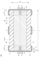
- 2 is a cross-sectional view of the multilayer ceramic capacitor 1 according to the first embodiment taken along line II-II in FIG. 3 is a cross-sectional view of the multilayer ceramic capacitor 1 in accordance with the first embodiment taken along line III-III in FIG. 2 is a cross-sectional view taken along an end face internal electrode 20 of the multilayer ceramic capacitor 1 according to the first embodiment.
- FIG. 2 is a cross-sectional view taken along a side surface internal electrode 50 of the multilayer ceramic capacitor 1 in accordance with the first embodiment.
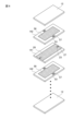
- 2A to 2C are diagrams illustrating a manufacturing process of a laminate 2 in a manufacturing method of the multilayer ceramic capacitor 1 in accordance with the first embodiment.
- FIG. 5 is a schematic perspective view of a multilayer ceramic capacitor 100 in accordance with a second embodiment.
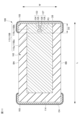
- 9 is a cross-sectional view of the multilayer ceramic capacitor 100 in accordance with the second embodiment taken along the line IX-IX in FIG. 8.
- 11 is a cross-sectional view taken along an internal electrode 115A on one end face side of the multilayer ceramic capacitor 100 in accordance with a second embodiment.
- FIG. 11 is a cross-sectional view taken along the inner electrode 115B on the other end face side of the multilayer ceramic capacitor 100 in accordance with the second embodiment.
- FIG. 5 is a schematic perspective view of a multilayer ceramic capacitor 100 in accordance with a second embodiment.
- 9 is a cross-sectional view of the multilayer ceramic capacitor 100 in accordance with the second embodiment taken along the line IX-IX in FIG. 8.
- 11 is a cross-sectional view taken along an internal electrode 115A on one end face side of the multilayer ceramic capacitor 100 in accordance with a second embodiment.
- Fig. 1 is a schematic perspective view of the multilayer ceramic capacitor 1.
- Fig. 2 is a cross-sectional view of the multilayer ceramic capacitor 1 taken along the II-II direction in Fig. 1.
- Fig. 3 is a cross-sectional view of the multilayer ceramic capacitor 1 taken along the III-III direction in Fig. 1.
- Fig. 4 is a cross-sectional view taken along the end face internal electrode 20 of the multilayer ceramic capacitor 1.
- Fig. 5 is a cross-sectional view taken along the side face internal electrode 50 of the multilayer ceramic capacitor 1.
- the multilayer ceramic capacitor 1 is a multilayer ceramic capacitor with a three-terminal structure, including a pair of end face external electrodes 3 provided on both end faces C in the length direction L of the laminate 2, and a pair of side face external electrodes 4 provided on both side faces B in the width direction W of the laminate 2.
- the laminate 2 includes an inner layer portion 11 in which a dielectric layer 14 and an internal electrode 15 are laminated, and an outer layer portion 12.
- the terminology used to indicate the orientation of the multilayer ceramic capacitor 1 refers to the direction in which the dielectric layers 14 and internal electrodes 15 are stacked in the multilayer ceramic capacitor 1 as the stacking direction T.
- the direction that intersects with the stacking direction T and in which the pair of end face external electrodes 3 are provided is referred to as the length direction L.
- the direction that intersects with both the length direction L and the stacking direction T is referred to as the width direction W.
- the stacking direction T, the length direction L, and the width direction W are mutually orthogonal.
- a pair of outer surfaces on both sides in the stacking direction T are referred to as main surfaces A
- a pair of outer surfaces extending in the stacking direction T and provided on both sides in the width direction W are referred to as side surfaces B
- a pair of outer surfaces extending in the stacking direction T and provided on both sides in the length direction L are referred to as end surfaces C.
- One of the main surfaces A is referred to as main surface AA
- main surface AB One of the side surfaces B
- side surface BA One of the side surfaces B
- One of the end surfaces C is referred to as end surface CA, and the other as end surface CB.
- the cross section in FIG. 2 is a cross section parallel to the length direction L and stacking direction T and passing through the center of the width direction W of the first pull-out section 22, and corresponds to the first reference cross section and the reference cross section in claim 1 of the claims.
- the cross section in FIG. 3 is a cross section parallel to the width direction W and stacking direction T and passing through the center of the length direction L of the second pull-out section 52, and corresponds to the second reference cross section and the reference cross section in claim 1 of the claims.
- the laminate 2 includes an inner layer portion 11 and outer layer portions 12 disposed on both sides of the inner layer portion 11 in the stacking direction T.
- the corners and ridges of the laminate 2 are preferably rounded. The corners are portions where three surfaces of the laminate intersect, and the ridges are portions where two surfaces of the laminate intersect.
- the inner layer portion 11 includes a plurality of dielectric layers 14 and internal electrodes 15 laminated in a lamination direction T.
- the dielectric layer 14 is made of a ceramic material.
- a dielectric ceramic containing BaTiO3 as a main component is used as the ceramic material.
- the ceramic material may be one containing at least one of a Mn compound, an Fe compound, a Cr compound, a Co compound, a Ni compound, or the like, added to the main component.
- the internal electrodes 15 are preferably made of a metal material such as Ni, Cu, Ag, Pd, an Ag-Pd alloy, or Au.
- the internal electrode 15 has a plurality of end face internal electrodes 20 and a plurality of side face internal electrodes 50 arranged alternately with each other. When there is no particular need to distinguish between the end face internal electrodes 20 and the side face internal electrodes 50, they may be collectively referred to as "internal electrodes 15." Furthermore, the internal electrode 15 corresponds to the internal electrode referred to in claim 1 of the claims.
- End surface internal electrode 20 As shown in FIG. 4, the end face internal electrodes 20 extend between both end faces C of the laminate 2 in the longitudinal direction L, and are spaced a certain distance from both side faces B in the width direction W.
- the electrode 20 has a first opposing portion 21 opposing the side surface internal electrode 50 adjacent in the stacking direction T, and a first extraction portion 22 extending from the first opposing portion 21 and exposed at each of the two end faces C. More specifically, the first opposing portion 21 is located in the center between both end faces C.
- the length direction L corresponds to the drawing direction of the first drawn portion 22.
- the side internal electrode 50 is slightly smaller than the laminate 2 and is spaced a certain distance from both end faces C in the length direction L.
- the end face internal electrode 20 has a second opposing portion 51 opposed to the adjacent end face internal electrode 20, and a second lead portion 52 led from the second opposing portion 51 and exposed on each of the two side faces B.
- the second opposing portion 51 is Specifically, the first opposing side wall 52 is located at the center between the two side walls B.
- the width direction W corresponds to the direction in which the second opposing side wall 52 is drawn out.
- the first drawn-out portion 21 and the second drawn-out portion 51 are collectively referred to as the "opposing portions 21, 51", and the first drawn-out portion 22 and the second drawn-out portion 52 are collectively referred to as the "draw-out portions 22, 52".
- the opposing portions 21 and 51 correspond to the opposing portions set forth in claim 1 of the appended claims, and the drawn-out portions 22 and 52 correspond to the drawn-out portions set forth in claim 1 of the appended claims.
- the dielectric layer 14 also has a first dielectric layer 141 on which the end surface internal electrode 20 is arranged, and a second dielectric layer 142 on which the side surface internal electrode 50 is arranged.
- the outer layer portion 12 is a dielectric layer of a constant thickness disposed on the main surface A side of the inner layer portion 11 (see FIGS. 2 and 3).
- the outer layer portion 12 is made of the same material as the dielectric layer 14 of the inner layer portion 11.
- End surface external electrode 3 A pair of end surface external electrodes 3 are respectively disposed on both end surfaces C of the laminate 2.
- a first lead portion 22 is connected to each end surface external electrode 3.
- Each end surface external electrode 3 covers not only each end surface C but also a portion of the end surface C side of the main surface A and the side surface B.
- Each end surface external electrode 3 includes a base electrode layer 31 and a plating layer 32 disposed on the base electrode layer 31.
- the plating layer 32 includes a Ni (nickel) plating layer 321 disposed on the base electrode layer 31, and a Sn (tin) plating layer 322 disposed on the Ni plating layer 321.
- Each side surface external electrode 4 covers not only the side surface B but also a part of the side surface B side of the main surface A.
- Each side surface external electrode 4 includes a base electrode layer 41 and a plating layer 42 disposed on the base electrode layer 41.
- the plating layer 42 includes a Ni (nickel) plating layer 421 disposed on the base electrode layer 41 and a Sn (tin) plating layer 422 disposed on the Ni plating layer 421.
- the end surface external electrode 3 and the side surface external electrode 4 may be collectively referred to as "external electrodes 3, 4".
- the external electrodes 3, 4 correspond to the external electrodes defined in claim 1 of the claims.
- first pull-out distance D1, first reference point P1, and first gap line G1 First pull-out distance D1, first reference point P1, and first gap line G1
- first lead distance D1 of each end face internal electrode 20 a point in each first lead portion 22 that is 2/3 of the first lead distance D1 away from one end face C to which the first lead portion 22 is led is defined as the first reference point P1 of each end face internal electrode 20.
- a line connecting the first reference points P1 adjacent to each other in the stacking direction T and a line connecting the first reference points P1 to each other in the stacking direction T are defined as the first gap line G1.
- Each first lead distance D1 is preferably the same. In that case, in the region on the one end face C side of the multilayer ceramic capacitor 1, each first reference point P1 is located on the same straight line extending in the stacking direction T, and the first gap line G1 is a straight line extending in the stacking direction T.
- the first lead portion 22 has a plurality of first through holes 23 penetrating in the stacking direction T.
- the same dielectric as the material of the dielectric layer 14 is disposed in each first through hole 23.
- the first lead portion 22 has a first columnar portion 27 that is disposed inside each first through hole 23, is the same dielectric as the material of the dielectric layer 14, and connects the dielectric layers 14 adjacent to each other in the stacking direction T across the first lead portion 22. This makes it possible to suppress peeling between the first lead portion 22 and the dielectric layer 14 adjacent to the first lead portion 22.
- the dimension of the first through hole 23 in the length direction L and the dimension of the first columnar portion 27 in the length direction L are approximately the same.
- the dimension of the first columnar portion 27 in the length direction L in the cross section of FIG. 2 is 20% to 80% of the first lead distance D1.
- the first through hole 23 provided in one first pull-out section 22 has a main first through hole 24 arranged at a position including the first reference point P1, and a sub-first through hole 25 arranged on the end face CA side of the main first through hole 24.
- the first column section 27 provided in the one first pull-out section 22 has a main first column section 28 arranged at a position including the first reference point P1, and a sub-first column section 29 arranged on the end face CA side of the main first column section 28.
- the main first column section 28 is located on the first gap line G1. This makes it possible to more effectively suppress peeling between layers.
- the dimension in the length direction L of the first main through hole 24 and the first main column portion 28 is 1/5 or more and 4/5 or less of the first pull-out distance D1 of the first pull-out portion 22 in which the first main through hole 24 and the first main column portion 28 are provided.
- a plurality of sub-first through holes 25 and sub-first column portions 29 are provided in one first pull-out section 22.
- the dimension in the length direction L of at least two or more of the sub-first through holes 25 and sub-first column portions 29 is smaller than the dimension in the length direction L of the main first through hole 24 and main first column portion 28 provided in the first pull-out section 22.
- the first pull-out portions 22 and the dielectric layers 14 are alternately arranged in the stacking direction T, and it is preferable that the first pull-out portion 22 having the first column portion 27 arranged at a position including the first reference point P1 (first gap line G1) and the dielectric layers 14 are continuous for a number of layers that is 3% or more of the total number of first pull-out portions 22 and dielectric layers 14 alternately arranged in the stacking direction T.
- the dielectric layer 14 sandwiched between two first pull-out portions 22 is considered to be a single layer even if it is a mixture of dielectrics derived from multiple ceramic green sheets.
- the number of outer layer portions 12 is not included in the number of dielectric layers 14.
- the number of end surface internal electrodes 20 in which the first through holes 23 and first columnar portions 27 are provided is preferably 1/5 or more of the total number of end surface internal electrodes 20.
- the end face internal electrode 20 adjacent to one of the main surfaces A is provided with a first through hole 23 and a first columnar portion 27.
- at least one end face internal electrode 20 of the end face internal electrodes 20 included in each region on both main surface A sides of the regions obtained by dividing the multilayer ceramic capacitor 1 into three equal parts in the stacking direction T has a first through hole 23 and a first columnar portion 27.
- the dimension in the stacking direction T of the end face internal electrode 20 having the first column portion 27 (main first column portion 28) located at a position including the first reference point P1 (first gap line G1) is preferably 0.1 ⁇ m or more and 5.0 ⁇ m or less.
- each second lead portion 52 extends from each second opposing portion 51 toward one side surface B (i.e., the dimension of the second lead portion 52 in the width direction W) is defined as the second lead distance D2 of each side surface internal electrode 50, and a point on each second lead portion 52 that is 2 ⁇ 3 of the second lead distance D2 away from the one side surface B from which the second lead portion 52 is led is defined as a second reference point P2 of each side surface internal electrode 50.
- a straight line connecting adjacent second reference points P2 in the stacking direction T and a line connecting them in the stacking direction T are defined as second gap lines G2.
- Each second lead distance D2 is preferably the same. In this case, in the region on one side B of the multilayer ceramic capacitor 1, the second reference points P2 are located on the same straight line extending in the stacking direction T, and the second gap line G2 forms a straight line extending in the stacking direction T.
- the first pull-out distance D1 and the second pull-out distance D2 are collectively referred to as the "pull-out distance D,” and the first reference point P1 and the second reference point P2 are collectively referred to as the “reference point P.”
- the pull-out distance D corresponds to the pull-out distance in claim 1 of the claims.
- the second drawn-out portion 52 has a plurality of second through holes 53 penetrating in the stacking direction T.
- a dielectric that is the same as the material of the dielectric layer 14 is disposed in each of the second through holes 53.
- the second drawn-out portion 52 has second column portions 57 that are disposed inside each of the second through holes 53, are the same dielectric as the material of the dielectric layer 14, and connect the dielectric layers 14 adjacent to each other in the stacking direction T with the second drawn-out portion 52 in between. This makes it possible to suppress peeling between the second drawn-out portion 52 and the dielectric layer 14 adjacent to the second drawn-out portion 52.
- the dimension of the width direction W of the second through hole 53 and the dimension of the width direction W of the second columnar portion 57 are approximately the same.
- the dimension of the width direction L of the second columnar portion 57 in the cross section of FIG. 3 is 20% to 80% of the second pull-out distance D2.
- the first through hole 23 and the second through hole 53 are collectively referred to as "through holes 23, 53"
- the first columnar portion 27 and the second columnar portion 57 are collectively referred to as "columnar portions 27, 57”.
- the through holes 23, 53 correspond to the through holes in claim 1 of the claims
- the columnar portions 27, 57 correspond to the columnar portions in claim 1 of the claims. It is not necessary for both the first through hole 23 and the first columnar portion 27 and the second through hole 53 and the second columnar portion 57 to be provided, and only one of them may be provided.
- the second through hole 53 has a main second through hole 35 arranged at a position including the second reference point P2, and a sub-second through hole 55 arranged on the side BA side of the main second through hole 35.
- the second column section 57 provided in the one second pull-out section 52 has a main second column section 58 arranged at a position including the second reference point P2, and a sub-second column section 59 provided on the side BA side of the main second column section 58.
- the main second column section 58 is located on the second gap line G2. This makes it possible to more effectively suppress peeling between layers.
- the dimension in the length direction L of the main second through hole 35 and the main second column portion 58 is 1/5 or more and 4/5 or less of the second pull-out distance D2 corresponding to the second pull-out portion 52 in which the main second through hole 35 and the main second column portion 58 are provided.
- one second pull-out section 52 is provided with a plurality of sub-second through holes 55 and sub-second column sections 59.
- the dimension in the width direction W of at least two or more of the sub-second through holes 55 and sub-second column sections 59 is smaller than the dimension in the width direction W of the main second through hole 35 and main second column section 58 provided in the second pull-out section 52.
- the second pull-out portions 52 and the dielectric layers 14 are alternately arranged in the stacking direction T, and it is preferable that the second pull-out portions 52 having the second column portions 57 arranged at a position including the second reference point P2 (second gap line G2) and the dielectric layers 14 are continuous for a number of layers that is 3% or more of the total number of layers of the second pull-out portions 52 and the dielectric layers 14 alternately arranged in the stacking direction T.
- the dielectric layer 14 sandwiched between two second pull-out portions 52 is considered to be a single layer even if it is a mixture of dielectrics derived from multiple ceramic green sheets.
- the number of outer layer portions 12 is not included in the number of dielectric layers 14.
- the number of side internal electrodes 50 in which the second through holes 53A and the second columnar portions 57A are provided is 1/5 or more of the total number of side internal electrodes 50.
- the side internal electrode 50 adjacent to one of the principal surfaces A is preferably provided with a second through hole 53 and a second columnar portion 57.
- at least one side internal electrode 50 preferably has a second through hole 53 and a second columnar portion 57.
- the dimension in the stacking direction T of the side internal electrode 50 in which the second column section 57 (main second column section 58) is provided on the second reference point P2 (second gap line G2) is preferably 0.1 ⁇ m or more and 5.0 ⁇ m or less.
- Fig. 6 is a diagram for explaining the steps for manufacturing the laminate 2 in the method for manufacturing the multilayer ceramic capacitor 1.
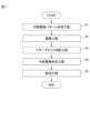
- Fig. 7 is a flow chart for explaining the method for manufacturing the multilayer ceramic capacitor 1.
- Ceramic green sheets are strip-shaped sheets made by forming a ceramic slurry containing ceramic powder, binder, and solvent onto a carrier film using a die coater, gravure coater, microgravure coater, etc.
- the end face internal electrode 20 and the side face internal electrode 50 are formed by printing, for example, screen printing, gravure printing, letterpress printing, or the like.
- a printing pattern of the end face internal electrode 20 in which the first through hole 23 is already provided, or a printing pattern of the side face internal electrode 50 in which the second through hole 53 is already provided it is possible to form the first through hole 23 in the end face internal electrode 20, or the second through hole 53 in the side face internal electrode 50.
- the method of forming the first through hole 23 and the second through hole 53 in the internal electrode 15 is not limited to this.
- Ceramic green sheets that become the first dielectric layer 141 on which the end face internal electrodes 20 are arranged and ceramic green sheets that become the second dielectric layer 142 on which the side face internal electrodes 50 are arranged are alternately laminated. Dielectrics originating from the dielectric layer 14 are arranged inside the first through holes 23 and inside the second through holes 53. This forms the first columnar section 27 and the second columnar section 57. Next, ceramic green sheets for the outer layer sections are arranged above and below and thermocompression bonded to form a mother block.
- End surface external electrodes 3 are formed on both end surfaces C of the laminate 2, and side surface external electrodes 4 are formed on both side surfaces B of the laminate 2.
- Each end surface external electrode 3 is formed so as to cover not only the end surface C but also a part of the end surface C side of the main surface A and the side surface B.
- the side surface external electrode 4 has The second lead portion 52 of the side surface internal electrode 50 is connected.
- Each side surface external electrode 4 is formed so as to cover not only the side surface B but also a part of the main surface A on the side surface B side.
- step S5 The laminate 2 on which the end surface external electrodes 3 and the side surface external electrodes 4 are arranged is heated in a nitrogen atmosphere at a set firing temperature for a predetermined time, thereby baking the end surface external electrodes 3 and the side surface external electrodes 4 onto the laminate 2, and the multilayer ceramic capacitor 1 shown in FIG.
- the first pull-out portion 22 has a first through hole 23 that penetrates the first pull-out portion 22 in the stacking direction T, and a first columnar portion 27 that is disposed within the first through hole 23 and is made of the same dielectric material as the dielectric layer 14, and connects adjacent dielectric layers 14 in the stacking direction T across the first pull-out portion 22, and the dimension of the first columnar portion 27 in the length direction L in the cross section of Figure 2 is 20% to 80% of the first pull-out distance D1.
- the second pull-out portion 52 also has a second through hole 53 that penetrates the second pull-out portion 52 in the stacking direction T, and a second columnar portion 57 that is disposed within the second through hole 53 and is made of the same dielectric material as the dielectric layer 14, and that connects adjacent dielectric layers 14 in the stacking direction T across the second pull-out portion 52, and the dimension of the second columnar portion 57 in the width direction W in the cross section of Figure 3 is 20% to 80% of the second pull-out distance D2.
- the column sections 27, 57 can prevent adjacent dielectric layers 14 in the stacking direction T across the pull-out sections 22, 52 from separating from each other, thereby effectively preventing delamination between layers in the multilayer ceramic capacitor 1.
- first column section 27 provided on the first pull-out section 22 is positioned at a position that includes the first reference point P1.
- the second pillar section 57 provided on the second pull-out section 52 is positioned at a position that includes the second reference point P2.
- the multiple first pull-out sections 22 and the multiple dielectric layers 14 are alternately arranged in the stacking direction T, and it is preferable that the first pull-out section 22 having the first column section 27 arranged at a position including the first reference point P1 and the dielectric layers 14 are continuous for a number of layers that is 3% or more of the total number of the first pull-out sections 22 and the dielectric layers 14 alternately arranged in the stacking direction T.
- the multiple second pull-out sections 52 and the multiple dielectric layers 14 are arranged alternately in the stacking direction T, and it is preferable that the second pull-out sections 52 having the second column sections 57 arranged at a position including the second reference point P2 and the dielectric layers 14 are continuous for a number of layers that is 3% or more of the total number of layers of the second pull-out sections 52 and the dielectric layers 14 arranged alternately in the stacking direction T.
- the dimension in the length direction L of the first column section 27 arranged at a position including the first reference point P1 is greater than or equal to 1/5 and less than or equal to 4/5 of the first pull-out distance D1 corresponding to the first reference point P1.
- the dimension of the width direction W of the second column portion 57 arranged at a position including the second reference point P2 is 1/5 or more and 4/5 or less of the second pull-out distance D2 corresponding to the second reference point P2.
- the first column portion 27 has a main first column portion 28 arranged at a position including the first reference point P1, and a sub-first column portion 29 arranged closer to the one end face C than the main first column portion 28, and the first drawer portion 22 having the main first column portion 28 and the sub-first column portion 29 has two or more sub-first column portions 29 whose dimension in the length direction L is smaller than the dimension in the length direction L of the main first column portion 28.
- the second column portion 57 has a main second column portion 58 arranged at a position including the second reference point P2, and a sub-second column portion 59 arranged on the one side B side of the main second column portion 58, and the second drawer portion 52 having the main second column portion 58 and the sub-second column portion 59 has two or more sub-second column portions 59 whose dimension in the width direction W is smaller than the dimension in the width direction W of the main second column portion 58.
- the number of end face internal electrodes 20 having the first columnar portion 27 arranged at a position including the first reference point P1 is 1/5 or more of the total number of end face internal electrodes 20.
- the number of side internal electrodes 50 having second columnar portions 57 arranged at a position including the second reference point P2 is 1/5 or more of the total number of side internal electrodes 50.
- the dimension in the stacking direction T of the end face internal electrode 20 having the first columnar portion 27 arranged at a position including the first reference point P1 is 0.1 ⁇ m or more and 5.0 ⁇ m or less.
- the dimension in the stacking direction T of the side internal electrode 50 having the second columnar portion 57 arranged at a position including the second reference point P2 is 0.1 ⁇ m or more and 5.0 ⁇ m or less.
- the multilayer ceramic capacitor 100 is a multilayer ceramic capacitor with a two-terminal structure.
- the following description will focus on the differences from the multilayer ceramic capacitor 1 according to the first embodiment, and the same components as those in the multilayer ceramic capacitor 1 according to the first embodiment will be denoted by the same reference numerals and description thereof will be omitted.
- FIG. 8 is a schematic perspective view of a multilayer ceramic capacitor 100 according to a second embodiment.
- FIG. 9 is a cross-sectional view of the multilayer ceramic capacitor 100 cut in the IX-IX direction in FIG. 8.
- FIG. 10 is a cross-sectional view taken along the internal electrode 115A on one end surface side of the multilayer ceramic capacitor 100.
- FIG. 11 is a cross-sectional view taken along the internal electrode 115B on the other end surface side of the multilayer ceramic capacitor 100.
- the cross section in FIG. 9 is a cross section parallel to the length direction L and the lamination direction T, and passing through the center of the lead-out portion 115b in the width direction W, and corresponds to the reference cross section.
- the multilayer ceramic capacitor 100 has a rectangular parallelepiped shape and includes a laminate 102 and a pair of external electrodes 103.
- the laminate 102 has a rectangular parallelepiped shape and includes an inner layer portion 111 and outer layer portions 112 arranged on both sides of the inner layer portion 111 in the stacking direction T.
- the inner layer 11 is made up of multiple dielectric layers 114 and internal electrodes 115 stacked in the stacking direction T.
- the internal electrode 115 has an internal electrode 115A on one end face side that is extended to the end face CA, and an internal electrode 115B on the other end face side that is extended to the end face CB.
- the internal electrode 115A on the one end face side and the internal electrode 115B on the other end face side are arranged alternately in the stacking direction T.
- the internal electrode 115A on one end face side has an opposing portion 115Aa located in the center between both end faces C, and an extended portion 115Ab on one end face side extending from the opposing portion 115Aa to the end face CA.
- the extended portion 115Ab on one end face side is exposed at the end face CA of the laminate 102.
- the internal electrode 115A on one end face side is spaced apart from the end face CB and both side faces B.
- the internal electrode 115B on the other end face side has an opposing portion 115Ba located in the center between both end faces C, and an extended portion 115Bb on the other end face side extending from the opposing portion 115Ba to the end face CB.
- the extended portion 115Bb on the other end face side is exposed at the end face CB of the laminate 102.
- the internal electrode 115B on the other end face side is spaced apart from the end face CA and both side faces B.
- opposing portion 115a the opposing portions 115Aa and 115Ba will be collectively referred to as "opposing portion 115a", and the pull-out portion 115Ab on one end face side and the pull-out portion 115Bb on the other end face side will be collectively referred to as "pull-out portion 115b”.
- Two external electrodes 103 are each disposed on end face C. Each external electrode 103 covers not only end face C, but also a portion of the main face A and side face B on the end face C side.
- the external electrode 103 includes an underlying electrode layer 104, a Ni plating layer 105 disposed on the underlying electrode layer 104, and a Sn plating layer 106 disposed on the Ni plating layer 105.
- An internal electrode 115A (lead portion 115Ab on one end face side) on one end face side is connected to the external electrode 103 on the end face CA side.
- An internal electrode 115B (lead portion 115Bb on the other end face side) on the other end face side is connected to the external electrode 103 on the end face CB side.
- the distance that the drawn-out portion 115b extends from the opposing portion 115a toward the one end face C from which the drawn-out portion 115b is drawn is defined as the draw-out distance D3.
- a point that is 2/3 of the draw-out distance D3 away from the one end face C from which the drawn-out portion 115b is drawn is defined as the reference point P3 of the internal electrode 115 (draw-out portion 115b).
- a line that connects adjacent reference points P3 in the stacking direction T and further connects them in the stacking direction T is defined as a gap line G3.
- each draw-out distance D3 is preferably the same. In that case, each reference point P3 is located on the same straight line extending in the stacking direction T, and each gap line G3 forms a straight line extending in the stacking direction T.
- the pull-out portion 115b has a plurality of through holes 121 penetrating in the stacking direction T.
- the same dielectric as the material of the dielectric layer 114 is disposed in each through hole 121.
- the pull-out portion 115b has a column portion 127 that is disposed inside each through hole 121, is made of the same dielectric as the material of the dielectric layer 114, and connects the adjacent dielectric layers 114 in the stacking direction T across the pull-out portion 115b. This makes it possible to suppress peeling between the pull-out portion 115b and the dielectric layer 114 adjacent to the pull-out portion 115b.
- the through holes 121 and the column portion 127 have a dimension in the length direction L in the cross section of FIG. 9 that is 20% to 80% of the pull-out distance.
- the through hole 121 has a main through hole 122 located at a position including the reference point P3, and a sub-through hole 123 located on the one end face C side of the main through hole 122.
- the column section 127 has a main column section 128 located at a position including the reference point P3, and a sub-column section 129 provided on the one end face C side from which the pull-out section 115b is pulled out, relative to the main column section 128.
- the main column section 128 is located on the gap line G3. This makes it possible to more effectively suppress delamination between layers.
- the dimension L of the main through hole 122 and the main column portion 128 in the length direction is 1/5 or more and 4/5 or less of the pull-out distance D3 corresponding to the pull-out portion 115b in which the main through hole 122 and the main column portion 128 are provided.
- one pull-out section 115b is preferably provided with a plurality of sub-through holes 123 and sub-column portions 129.
- the dimension in the length direction L of at least two of the sub-through holes 123 and sub-column portions 129 is preferably smaller than the dimension in the length direction L of the main through hole 122 and main column portion 128 provided in the pull-out section 115b.
- the pull-out portions 115b and the dielectric layers 114 are alternately arranged in the stacking direction T. It is preferable that the pull-out portions 115b having the pillar portions 127 on the reference point P3 (gap line G3) and the dielectric layers 114 are continuous for a number of layers that is 3% or more of the total number of the pull-out portions 115b and the dielectric layers 114 alternately arranged in the stacking direction T. Note that the dielectric layer 114 sandwiched between the two pull-out portions 115b is considered to be a single layer even if it is a mixture of dielectrics derived from multiple ceramic green sheets. The number of the dielectric layers 114 does not include the number of the outer layer portions 112.
- the number of internal electrodes 115 in which through holes 121 and column portions 127 are provided is 1/5 or more of the total number of internal electrodes 115.
- the internal electrode 115 adjacent to one of the principal surfaces A is preferably provided with a through hole 121 and a column portion 127.
- at least one internal electrode 115 preferably has a through hole 121 and a column portion 127.
- the dimension of the internal electrode 115 in the stacking direction T, in which the pillar portion 127 (main pillar portion 128) is provided on the reference point P3 (gap line G3), is preferably 0.1 ⁇ m or more and 5.0 ⁇ m or less.
- a ceramic green sheet is prepared by printing a pattern of the internal electrodes 115 with a conductive paste on a ceramic green sheet for lamination, which is formed by forming a ceramic slurry into a sheet.
- the through holes 121 can be formed in the internal electrodes 115 by using the printed pattern of the internal electrodes 115 in which the through holes 121 have already been formed.
- multiple ceramic green sheets are stacked so that the internal electrode patterns are shifted by half a pitch between adjacent ceramic green sheets in the longitudinal direction.
- ceramic green sheets for the outer layers are arranged one above the other and thermocompression bonded to form a mother block.
- the mother block is cut and divided in the longitudinal direction L and the width direction W to produce multiple rectangular laminates 102.
- external electrodes 103 are formed on both end faces C of the laminate 102.
- the laminate 102 with the external electrodes 103 disposed thereon is heated in a nitrogen atmosphere at a set firing temperature for a predetermined time. This causes the external electrodes 103 to be baked onto the laminate 102, and the laminated ceramic capacitor 100 shown in FIG. 1 is obtained.
- the pull-out portion 115b has a through hole 121 that passes through the pull-out portion 115b in the stacking direction T, and a pillar portion 127 that is disposed within the through hole 121 and is made of the same dielectric material as the dielectric layer 114, and that connects adjacent dielectric layers 114 in the stacking direction T across the pull-out portion 115b.
- the dimension of the length direction L of the pillar portion 127 is 20% to 80% of the pull-out distance D3.
- the column portion 127 can prevent the adjacent dielectric layers 114 in the stacking direction T across the pull-out portion 115b from separating from each other, so that delamination between layers can be effectively prevented in the multilayer ceramic capacitor 100, which is a two-terminal type multilayer ceramic capacitor.
- the multiple pull-out portions 115b and the multiple dielectric layers 114 are arranged alternately in the stacking direction T, and it is preferable that the pull-out portion 115b having the column portion 127 arranged at a position including the reference point P3 and the dielectric layer 114 are continuous for a number of layers that is 3% or more of the total number of the pull-out portions 115b and the dielectric layers 114 arranged alternately in the stacking direction T.
- the dimension in the length direction L of the column portion 127 arranged at a position including the reference point P3 is 1/5 or more and 4/5 or less of the pull-out distance D3 corresponding to the reference point P3.
- the pillar portion 127 in the region of the cross section of Figure 9 near one end face C, has a main pillar portion 128 arranged at a position including the reference point P3, and a sub-pillar portion 129 arranged on the one end face C side of the main pillar portion 128, and the drawer portion 115b having the main pillar portion 128 and the sub-pillar portion 129 has two or more sub-pillar portions 129 whose dimension in the length direction L is smaller than the dimension in the length direction L of the main pillar portion 128.
- the number of internal electrodes 115 having column portions 127 arranged at a position including the reference point P3 is preferably 1/5 or more of the total number of internal electrodes 115 connected to that one end face C.
- the dimension in the stacking direction T of the internal electrode 115 having the column portion 127 arranged at a position including the reference point P3 is 0.1 ⁇ m or more and 5.0 ⁇ m or less.
- the multilayer ceramic capacitor 1 is a three-terminal multilayer ceramic capacitor, but the multilayer ceramic capacitor may be a multi-terminal type having more external electrodes.
- side B has a plurality of external electrodes arranged side by side in the length direction.
- the internal electrodes include internal electrodes that are drawn out to the two side faces B, and each internal electrode drawn out to one of the two side faces B has a plurality of drawn-out portions that are arranged in the length direction L. The drawn-out portions are drawn out to side face B and connected to external electrodes arranged on side face B.
- the desired effects can also be obtained with a multi-terminal multilayer ceramic capacitor.
- the present invention also includes the following combinations:
- a laminate including a plurality of laminated dielectric layers and a plurality of internal electrodes respectively arranged on the plurality of dielectric layers, the laminate having two main surfaces facing each other in the lamination direction, two side surfaces facing each other in a width direction perpendicular to the lamination direction, and two end surfaces facing each other in a length direction perpendicular to the lamination direction and the width direction, and an external electrode connected to the internal electrode on at least one of the side surfaces and the end surfaces, wherein the internal electrode has an opposing portion facing the internal electrode adjacent to the lamination direction, and a pull-out portion drawn from the opposing portion to at least one of the side surfaces and the end surfaces, and the pull-out portion has a through hole penetrating the pull-out portion in the lamination direction, and a through hole extending from the through hole to the inner surface of the through hole.
- the direction in which the pull-out portion in which one of the column portions is provided is pulled out from the opposing portion is defined as the pull-out direction corresponding to the column portion
- a cross section that is parallel to the pull-out direction and the stacking direction and passes through the center of the pull-out portion in a direction perpendicular to the pull-out direction and the stacking direction is defined as a reference cross section
- the distance that the pull-out portion extends from the opposing portion toward one of the side surfaces or end faces from which the pull-out portion is pulled out is defined as a pull-out distance in the reference cross section
- the dimension of the column portion in the pull-out direction in the reference cross section is 20% to 80% of the pull-out distance.
- a laminate including a plurality of laminated dielectric layers and a plurality of internal electrodes respectively arranged on the plurality of dielectric layers, the laminate having two main surfaces facing each other in the lamination direction, two side surfaces facing each other in a width direction perpendicular to the lamination direction, and two end surfaces facing each other in a length direction perpendicular to the lamination direction and the width direction, two end face external electrodes respectively arranged on the two end faces, and two side face external electrodes respectively arranged on the two side faces, wherein the plurality of internal electrodes include an end face internal electrode connected to the two end face external electrodes, and a side face internal electrode connected to the two side face external electrodes, and the end face internal electrode has a first opposing portion facing the side face internal electrode adjacent to the lamination direction, and a first extraction portion drawn from the first opposing portion and exposed to the two end faces, and the side face internal electrodes A multilayer ceramic capacitor in which the electrodes have a second opposing portion facing the end face internal electrodes adjacent in the stack
- the second pull-out portion has a second through hole penetrating the second pull-out portion in the stacking direction, and a second columnar portion disposed within the second through hole, made of the same dielectric material as the dielectric layers, and connecting the dielectric layers adjacent in the stacking direction with the second pull-out portion in between, and the second reference cross section is a cross section that is parallel to the width direction and the stacking direction and passes through the center of the second pull-out portion in the length direction, and the distance that the second pull-out portion extends from the second opposing portion toward one of the end faces in the second reference cross section is a second pull-out distance, the width dimension of the second columnar portion in the second reference cross section is 20% to 80% of the second pull-out distance.
- a laminate including a plurality of laminated dielectric layers and a plurality of internal electrodes respectively arranged on the plurality of dielectric layers, the laminate having two main surfaces facing each other in the lamination direction, two side surfaces facing each other in a width direction perpendicular to the lamination direction, and two end surfaces facing each other in a length direction perpendicular to the lamination direction and the width direction, two end face external electrodes respectively arranged on the two end faces, and two side face external electrodes respectively arranged on the two side faces, wherein the plurality of internal electrodes include an end face internal electrode connected to the two end face external electrodes, and a side face internal electrode connected to the two side face external electrodes, and the end face internal electrode has a first opposing portion facing the side face internal electrode adjacent to the lamination direction, and a first extraction portion drawn out from the first opposing portion and exposed to the two end faces, and the side face internal The electrodes have a second opposing portion that faces the end face internal electrodes adjacent in the stacking direction, and a second
- ⁇ 5> The multilayer ceramic capacitor described in ⁇ 2> or ⁇ 3>, in which, when a point on one of the first pull-out sections, which is a distance of 2/3 of the first pull-out distance from one of the end faces from which the first pull-out section is pulled, is defined as a first reference point, the first pillar section provided on the first pull-out section is disposed at a position including the first reference point.
- ⁇ 6> The multilayer ceramic capacitor described in ⁇ 3> or ⁇ 4>, in which, when a point on one of the second pull-out sections in the second reference cross section is a point that is 2/3 of the second pull-out distance away from one of the side surfaces from which the second pull-out section is pulled out, the second pillar section provided on the second pull-out section is disposed at a position that includes the second reference point.
- the first column portion has a main first column portion arranged at a position including the first reference point and a sub-first column portion arranged closer to the one of the end faces than the main first column portion, and the first pull-out portion having the main first column portion and the sub-first column portion has two or more sub-first column portions whose lengthwise dimension is smaller than the lengthwise dimension of the main first column portion.
- a multilayer ceramic capacitor as described in any one of ⁇ 5>, ⁇ 7>, and ⁇ 9>.
- the second column portion has a main second column portion arranged at a position including the second reference point and a sub-second column portion arranged closer to the one of the side surfaces than the main second column portion, and the second pull-out portion having the main second column portion and the sub-second column portion has two or more sub-second column portions whose width dimension is smaller than the width dimension of the main second column portion.
- ⁇ 14> A multilayer ceramic capacitor according to any one of ⁇ 6>, ⁇ 8>, ⁇ 10> and ⁇ 12>, in which the number of the side internal electrodes having the second columnar portion arranged at a position including the second reference point is 1/5 or more of the total number of the side internal electrodes.
- a multilayer ceramic capacitor comprising a laminate including a plurality of laminated dielectric layers and a plurality of internal electrodes respectively arranged on the plurality of dielectric layers, the laminate having two main surfaces facing each other in the lamination direction, two side surfaces facing each other in a width direction perpendicular to the lamination direction, and two end faces facing each other in a length direction perpendicular to the lamination direction and the width direction, and two external electrodes respectively arranged on the two end faces, wherein each of the plurality of internal electrodes is connected to one of the two external electrodes, and has an opposing portion facing the internal electrode adjacent to the lamination direction, and an external electrode extending from the opposing portion and extending between one of the two end faces.
- a multilayer ceramic capacitor having a pull-out portion exposed on either side, the pull-out portion having a through hole penetrating the pull-out portion in the stacking direction, and a column portion disposed in the through hole, the column portion being a dielectric of the same material as the dielectric layers and connecting the adjacent dielectric layers in the stacking direction across the pull-out portion, the reference cross section being a cross section parallel to the length direction and the stacking direction and passing through the center of the pull-out portion in the width direction, and the distance the pull-out portion extends from the opposing portion toward one of the end faces on the reference cross section being the pull-out distance, the lengthwise dimension of the column portion on the reference cross section being 20% to 80% of the pull-out distance.
- a multilayer ceramic capacitor according to any one of ⁇ 18> to ⁇ 20> in which, in a region of the reference cross section close to one of the end faces, the column portion has a main column portion arranged at a position including the reference point and a sub-column portion arranged closer to the one of the end faces than the main column portion, and the draw-out portion having the main column portion and the sub-column portion has two or more sub-columns whose dimension in the length direction is smaller than the dimension in the length direction of the main column portion.
Landscapes
- Engineering & Computer Science (AREA)
- Power Engineering (AREA)
- Manufacturing & Machinery (AREA)
- Microelectronics & Electronic Packaging (AREA)
- Chemical & Material Sciences (AREA)
- Ceramic Engineering (AREA)
- Inorganic Chemistry (AREA)
- Fixed Capacitors And Capacitor Manufacturing Machines (AREA)
- Ceramic Capacitors (AREA)
Abstract
L'invention propose un condensateur céramique multicouche avec lequel il est possible de supprimer de manière appropriée le délaminage. Un condensateur céramique multicouche (1) comprend un stratifié (2) qui comporte une couche diélectrique (14) et une électrode interne (15). L'électrode interne (15) possède des parties opposées (21, 51) et des parties étirées (22, 52) qui sont tirées vers au moins l'une d'une surface latérale B et d'une surface d'extrémité C du stratifié (2). Les parties étirées (22, 52) comportent des trous traversants (23, 53) et des parties de colonne (27, 57) qui sont disposées dans les trous traversants (23, 53). Les parties de colonne sont des corps diélectriques constitués du même matériau que la couche diélectrique (14), et relient des couches diélectriques (14) qui sont adjacentes l'une à l'autre dans une direction de stratification T de façon à prendre en sandwich les parties étirées (22, 52) entre elles. Lorsque la direction dans laquelle les parties étirées (22, 52) sont tirées depuis des parties opposées (21, 51) est définie comme étant la direction de tirage, et la distance d'extension des parties étirées (22, 52) des parties opposées (21, 51) vers la surface latérale B ou la surface d'extrémité C est définie comme la distance de tirage D, la dimension des parties de colonne (27, 57) dans la direction de tirage dans la section transversale de la figure 2 ou 3 est de 20 % à 80 % inclus de la distance de tirage D.
Priority Applications (1)
| Application Number | Priority Date | Filing Date | Title |
|---|---|---|---|
| US19/311,407 US20250378995A1 (en) | 2023-04-19 | 2025-08-27 | Multilayer ceramic capacitor |
Applications Claiming Priority (2)
| Application Number | Priority Date | Filing Date | Title |
|---|---|---|---|
| JP2023068357 | 2023-04-19 | ||
| JP2023-068357 | 2023-04-19 |
Related Child Applications (1)
| Application Number | Title | Priority Date | Filing Date |
|---|---|---|---|
| US19/311,407 Continuation US20250378995A1 (en) | 2023-04-19 | 2025-08-27 | Multilayer ceramic capacitor |
Publications (1)
| Publication Number | Publication Date |
|---|---|
| WO2024219092A1 true WO2024219092A1 (fr) | 2024-10-24 |
Family
ID=93152645
Family Applications (1)
| Application Number | Title | Priority Date | Filing Date |
|---|---|---|---|
| PCT/JP2024/007530 Ceased WO2024219092A1 (fr) | 2023-04-19 | 2024-02-29 | Condensateur céramique multicouche |
Country Status (2)
| Country | Link |
|---|---|
| US (1) | US20250378995A1 (fr) |
| WO (1) | WO2024219092A1 (fr) |
Citations (9)
| Publication number | Priority date | Publication date | Assignee | Title |
|---|---|---|---|---|
| JPS5822728U (ja) * | 1981-08-04 | 1983-02-12 | 株式会社村田製作所 | 積層セラミツクコンデンサ |
| JPS5889926U (ja) * | 1981-12-11 | 1983-06-17 | ティーディーケイ株式会社 | 貫通コンデンサ |
| JPS6083234U (ja) * | 1983-11-14 | 1985-06-08 | 株式会社ケンウッド | 積層コンデンサ |
| JPH0268429U (fr) * | 1988-11-15 | 1990-05-24 | ||
| JPH0897071A (ja) * | 1994-09-29 | 1996-04-12 | Kyocera Corp | 積層型磁器コンデンサ |
| JPH1022172A (ja) * | 1996-06-29 | 1998-01-23 | Taiyo Yuden Co Ltd | 積層電子部品とその製造方法 |
| JP2005072149A (ja) * | 2003-08-21 | 2005-03-17 | Tdk Corp | 積層コンデンサ |
| JP2006120698A (ja) * | 2004-10-19 | 2006-05-11 | Murata Mfg Co Ltd | 積層セラミック電子部品およびその製造方法 |
| JP2022104530A (ja) * | 2020-12-28 | 2022-07-08 | サムソン エレクトロ-メカニックス カンパニーリミテッド. | 積層型キャパシタ及びその実装基板 |
-
2024
- 2024-02-29 WO PCT/JP2024/007530 patent/WO2024219092A1/fr not_active Ceased
-
2025
- 2025-08-27 US US19/311,407 patent/US20250378995A1/en active Pending
Patent Citations (9)
| Publication number | Priority date | Publication date | Assignee | Title |
|---|---|---|---|---|
| JPS5822728U (ja) * | 1981-08-04 | 1983-02-12 | 株式会社村田製作所 | 積層セラミツクコンデンサ |
| JPS5889926U (ja) * | 1981-12-11 | 1983-06-17 | ティーディーケイ株式会社 | 貫通コンデンサ |
| JPS6083234U (ja) * | 1983-11-14 | 1985-06-08 | 株式会社ケンウッド | 積層コンデンサ |
| JPH0268429U (fr) * | 1988-11-15 | 1990-05-24 | ||
| JPH0897071A (ja) * | 1994-09-29 | 1996-04-12 | Kyocera Corp | 積層型磁器コンデンサ |
| JPH1022172A (ja) * | 1996-06-29 | 1998-01-23 | Taiyo Yuden Co Ltd | 積層電子部品とその製造方法 |
| JP2005072149A (ja) * | 2003-08-21 | 2005-03-17 | Tdk Corp | 積層コンデンサ |
| JP2006120698A (ja) * | 2004-10-19 | 2006-05-11 | Murata Mfg Co Ltd | 積層セラミック電子部品およびその製造方法 |
| JP2022104530A (ja) * | 2020-12-28 | 2022-07-08 | サムソン エレクトロ-メカニックス カンパニーリミテッド. | 積層型キャパシタ及びその実装基板 |
Also Published As
| Publication number | Publication date |
|---|---|
| US20250378995A1 (en) | 2025-12-11 |
Similar Documents
| Publication | Publication Date | Title |
|---|---|---|
| US12040136B2 (en) | Multilayer ceramic capacitor with reduced equivalent series inductance | |
| US12431286B2 (en) | Multilayer ceramic capacitor including raised portions thicker from middle portion towards outer periphery | |
| US11476046B2 (en) | Multilayer ceramic capacitor | |
| KR102412702B1 (ko) | 적층 세라믹 콘덴서, 및 적층 세라믹 콘덴서의 제조 방법 | |
| JP7234951B2 (ja) | 積層セラミックコンデンサ | |
| JP7548195B2 (ja) | 積層セラミックコンデンサ | |
| KR20220040994A (ko) | 적층 세라믹 콘덴서 | |
| KR102871469B1 (ko) | 적층 세라믹 콘덴서 | |
| KR102762876B1 (ko) | 적층형 전자 부품 | |
| JP5769487B2 (ja) | コンデンサ | |
| JP7765987B2 (ja) | 積層セラミックコンデンサ | |
| JP7247559B2 (ja) | 積層セラミックコンデンサおよび積層セラミックコンデンサの製造方法 | |
| WO2024135066A1 (fr) | Condensateur céramique multicouche | |
| US20250378995A1 (en) | Multilayer ceramic capacitor | |
| US20250029789A1 (en) | Multilayer ceramic capacitor | |
| WO2025028129A1 (fr) | Condensateur céramique multicouche | |
| WO2023233835A1 (fr) | Condensateur céramique multicouche | |
| JP2005032807A (ja) | 積層セラミック電子部品およびその製造方法 | |
| US20250372312A1 (en) | Multilayer ceramic capacitor | |
| WO2025033017A1 (fr) | Condensateur céramique multicouche | |
| WO2025028131A1 (fr) | Condensateur céramique multicouche | |
| JP2025134124A (ja) | 積層セラミック電子部品 | |
| JP2025103740A (ja) | 積層セラミックコンデンサ | |
| JP2024141302A (ja) | 積層セラミックコンデンサ | |
| WO2025134454A1 (fr) | Condensateur céramique multicouche |
Legal Events
| Date | Code | Title | Description |
|---|---|---|---|
| 121 | Ep: the epo has been informed by wipo that ep was designated in this application |
Ref document number: 24792368 Country of ref document: EP Kind code of ref document: A1 |
|
| NENP | Non-entry into the national phase |
Ref country code: DE |
|
| 122 | Ep: pct application non-entry in european phase |
Ref document number: 24792368 Country of ref document: EP Kind code of ref document: A1 |