WO2024241702A1 - 情報処理装置および撮像装置 - Google Patents
情報処理装置および撮像装置 Download PDFInfo
- Publication number
- WO2024241702A1 WO2024241702A1 PCT/JP2024/012563 JP2024012563W WO2024241702A1 WO 2024241702 A1 WO2024241702 A1 WO 2024241702A1 JP 2024012563 W JP2024012563 W JP 2024012563W WO 2024241702 A1 WO2024241702 A1 WO 2024241702A1
- Authority
- WO
- WIPO (PCT)
- Prior art keywords
- image
- information
- imaging device
- background
- processing
- Prior art date
- Legal status (The legal status is an assumption and is not a legal conclusion. Google has not performed a legal analysis and makes no representation as to the accuracy of the status listed.)
- Ceased
Links
Images






Classifications
-
- H—ELECTRICITY
- H04—ELECTRIC COMMUNICATION TECHNIQUE
- H04N—PICTORIAL COMMUNICATION, e.g. TELEVISION
- H04N23/00—Cameras or camera modules comprising electronic image sensors; Control thereof
- H04N23/70—Circuitry for compensating brightness variation in the scene
- H04N23/76—Circuitry for compensating brightness variation in the scene by influencing the image signals
-
- G—PHYSICS
- G06—COMPUTING OR CALCULATING; COUNTING
- G06T—IMAGE DATA PROCESSING OR GENERATION, IN GENERAL
- G06T7/00—Image analysis
- G06T7/10—Segmentation; Edge detection
- G06T7/194—Segmentation; Edge detection involving foreground-background segmentation
-
- H—ELECTRICITY
- H04—ELECTRIC COMMUNICATION TECHNIQUE
- H04N—PICTORIAL COMMUNICATION, e.g. TELEVISION
- H04N23/00—Cameras or camera modules comprising electronic image sensors; Control thereof
- H04N23/60—Control of cameras or camera modules
-
- H—ELECTRICITY
- H04—ELECTRIC COMMUNICATION TECHNIQUE
- H04N—PICTORIAL COMMUNICATION, e.g. TELEVISION
- H04N23/00—Cameras or camera modules comprising electronic image sensors; Control thereof
- H04N23/60—Control of cameras or camera modules
- H04N23/67—Focus control based on electronic image sensor signals
- H04N23/672—Focus control based on electronic image sensor signals based on the phase difference signals
-
- H—ELECTRICITY
- H04—ELECTRIC COMMUNICATION TECHNIQUE
- H04N—PICTORIAL COMMUNICATION, e.g. TELEVISION
- H04N23/00—Cameras or camera modules comprising electronic image sensors; Control thereof
- H04N23/60—Control of cameras or camera modules
- H04N23/68—Control of cameras or camera modules for stable pick-up of the scene, e.g. compensating for camera body vibrations
- H04N23/682—Vibration or motion blur correction
- H04N23/685—Vibration or motion blur correction performed by mechanical compensation
- H04N23/687—Vibration or motion blur correction performed by mechanical compensation by shifting the lens or sensor position
-
- H—ELECTRICITY
- H04—ELECTRIC COMMUNICATION TECHNIQUE
- H04N—PICTORIAL COMMUNICATION, e.g. TELEVISION
- H04N23/00—Cameras or camera modules comprising electronic image sensors; Control thereof
- H04N23/70—Circuitry for compensating brightness variation in the scene
- H04N23/71—Circuitry for evaluating the brightness variation
-
- H—ELECTRICITY
- H04—ELECTRIC COMMUNICATION TECHNIQUE
- H04N—PICTORIAL COMMUNICATION, e.g. TELEVISION
- H04N5/00—Details of television systems
- H04N5/222—Studio circuitry; Studio devices; Studio equipment
-
- G—PHYSICS
- G06—COMPUTING OR CALCULATING; COUNTING
- G06T—IMAGE DATA PROCESSING OR GENERATION, IN GENERAL
- G06T2207/00—Indexing scheme for image analysis or image enhancement
- G06T2207/10—Image acquisition modality
- G06T2207/10024—Color image
Definitions
- the present invention relates to an information processing device that processes information related to imaging.
- One imaging technique used in movies and television is virtual production, in which a background image is displayed on a background display that is larger than the subject, and then the subject is imaged together with the background image.
- LEDs which are the display elements primarily used in background displays, have viewing angle characteristics. For this reason, if the imaging device is not positioned so as to directly face the background display when imaging, image quality unevenness (brightness unevenness) will occur in the background image area in the image data obtained by imaging.
- Patent document 1 discloses a method for calculating the angle between an LED display and an imaging device from position information of the imaging device, and correcting the brightness of the LED display using a brightness correction value according to the angle.
- the present invention provides an information processing device and an imaging device that can obtain image data with reduced image quality unevenness in the background image area, regardless of the arrangement of the background display and the imaging device.
- An information processing device as one aspect of the present invention is characterized by having an acquisition means for acquiring an input image obtained by capturing an image of a subject and a background image displayed on a background display using an imaging device, a discrimination means for discriminating between a subject area and a background image area in the input image, and a processing means for acquiring arrangement information regarding at least one of the angle and distance between the background display and the imaging device, and performing image processing on the background image area according to the arrangement information.
- an imaging device having the above-mentioned information processing device also constitutes another aspect of the present invention.
- An information processing method as another aspect of the present invention is characterized by having the steps of acquiring an input image obtained by capturing an image of a subject and a background image displayed on a background display using an imaging device, determining the subject area and the background image area in the input image, and acquiring position information regarding at least one of the angle and distance between the background display and the imaging device, and performing image processing on the background image area according to the position information.
- a program for causing a computer to execute processing according to the above information processing method also constitutes another aspect of the present invention.
- the present invention it is possible to obtain an image with reduced image quality unevenness in the background image area, regardless of the arrangement of the background display and the imaging device.
- FIG. 1 is a block diagram showing a configuration of an imaging apparatus according to an embodiment.
- FIG. 2 is a diagram showing a part of a light receiving surface of an image sensor.
- 11 is a flowchart showing a process for calculating distance information in the embodiment.
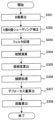
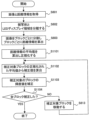
- FIG. FIG. 4 is a flowchart showing a process in the first embodiment.
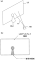
- 3A and 3B are diagrams showing an image capturing state in the first embodiment and a subject area and an LED display area in the image data.
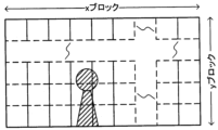
- FIG. 4 is a diagram showing division of image data in the first embodiment.
- 4A and 4B are diagrams showing a correction target block and peripheral blocks in the first embodiment.
- 5 is a schematic diagram showing an imaging position and two adjacent blocks on adjacent LED displays in image data in the first embodiment.
- FIG. 10 is a flowchart showing a process according to a second embodiment.
- FIG. 1 shows the configuration of an image capture device 100.
- the image capture device 100 captures images, processes the images, and records the images.
- Each unit connected to the internal bus 101 can exchange data with each other via the internal bus 101.
- Lens unit 106 has an optical system including a zoom lens, a focus lens, and an aperture mechanism, and a motor that drives the optical system.
- the optical image formed by lens unit 106 is converted into an image signal as an analog electrical signal (i.e., imaged) by an image sensor such as a CCD sensor or CMOS sensor included in imaging unit 107.
- Imaging unit 107 also includes an A/D conversion unit that converts the image signal output from the image sensor into a digital signal (image data).
- the image sensor is an image plane phase difference sensor, and details of this will be described later.
- the CPU 102 as a computer controls each part of the imaging device 100 according to a program stored in the ROM 103, using the RAM 104 as a work memory.
- ROM 103 is a non-volatile memory that records programs and various parameters for operating CPU 102.
- RAM 104 is a volatile memory.
- Frame memory 111 is a memory that temporarily stores image data, and allows image data to be read out when necessary. Using frame memory 111, it is possible to perform processes such as combining images obtained by capturing images at different times and cutting out specific areas from images obtained by capturing images.
- the image processing unit 105 as an information processing device performs various image processing on image data from the imaging unit 107 or image data stored in the frame memory 111 or recording medium 112 under the control of the CPU 102.
- the image processing performed by the image processing unit 105 includes pixel interpolation, encoding, compression, decoding, enlargement/reduction (resizing), noise reduction, color conversion, and the like.
- the image processing unit 105 also corrects performance variations in multiple pixels of the imaging element, corrects defective pixels, corrects white balance, corrects brightness, and corrects distortion and peripheral light loss caused by lens characteristics.
- the image processing unit 105 generates distance information, which will be described later, and performs brightness value correction of image data according to the angle and distance between the background display and the imaging device 100, which will be described later.
- the image processing unit 105 may be configured as a dedicated image processing computer that performs image processing, or the CPU 102 may have the functions of the image processing unit 105.
- the CPU 102 controls each motor of the lens unit 106 based on the calculation results for lens control obtained from the image processing unit 105 to perform optical zoom, focusing, and aperture adjustment.
- the CPU 102 may also perform image blur correction by moving a lens that constitutes part of the optical system in a direction perpendicular to the optical axis in response to camera shake detected by the attitude detection unit 116, which will be described later.
- the operation unit 113 accepts operations by the user and outputs instructions corresponding to the operations to the CPU 102 and the image processing unit 105.
- the operation unit 113 has operation members such as switches, dials, and buttons.
- the operation members include a power switch, a mode switching dial, and a release button.
- AF autofocus
- AE exposure control
- the operation unit 113 may be a touch sensor provided on the display unit 114.
- the display unit 114 which serves as a display means, displays images processed by the image processing unit 105, setting menus, etc.
- the display unit 114 has a display device such as an LCD (Liquid Crystal Display) or an organic EL (Electroluminescence).
- the display unit 114 may also be provided with the touch sensor described above.
- the CPU 102 generates text information and icons to inform the user of the settings of the imaging device 100, as well as images of setting menus for configuring various settings of the imaging device 100, and displays these on the display unit 114 by superimposing them on the image processed by the image processing unit 105.
- Video terminal 109 is a terminal for a video interface such as SDI (Serial Digital Interface), HDMI (High Definition Multimedia Interface) (registered trademark), DisplayPort (registered trademark), etc.
- CPU 102 can output video (image data) to an external monitor, etc. via video terminal 109.
- the network module 108 is an interface for inputting and outputting image data and audio signals.
- the CPU 102 communicates with external devices via the Internet, etc. through the network module 108, and can transmit and receive not only image data and audio signals, but also control signals such as commands.
- the network module 108 may be of either a wireless communication type or a wired communication type.
- the recording medium 112 is a hard disc drive (HDD) or solid state drive (SSD) capable of recording image data and various setting data, and is removably attached to the recording medium I/F 110.
- HDD hard disc drive
- SSD solid state drive
- the object detection unit 115 detects objects using artificial intelligence such as deep learning using a neural network.
- the CPU 102 transmits programs, network structures, weight parameters, etc. stored in the ROM 103 to the object detection unit 115. Examples of network structures include SSD (Single Shot Multibox Detector) and YOLO (You Only Look Once).
- the object detection unit 115 performs processing to detect objects from image data based on various parameters obtained from the CPU 102, and sends the processing results to the RAM 104.
- the attitude detection unit 116 detects the attitude and shake of the imaging device 100 using an angular velocity sensor, an acceleration sensor, etc. This makes it possible to detect the tilt of the imaging device 100, camera shake due to hand shake, etc.
- FIG. 2(A) shows a schematic diagram of a part of an image sensor in which red (R), blue (B), and green (Gb, Gr) pixels are arranged in a Bayer array.
- each pixel has two photodiodes A and B as photoelectric conversion elements, and the two photodiodes A and B are provided with one microlens (not shown).
- the imaging unit 107 generates a pair of image signals (A and B image signals) for phase difference detection by synthesizing the A and B signals output from each of the multiple pixels on the image sensor.
- an imaging signal for obtaining image data is generated by adding the A and B image signals.
- the imaging unit 107 in addition to outputting an A signal and a B signal from each pixel, it is also possible to output a value obtained by averaging the A signals and B signals from multiple pixels that are close to each other. By outputting the averaged value, it is possible to shorten the time it takes to read signals from the imaging unit 107 and reduce the bandwidth of the internal bus 101.
- the CPU 102 performs a correlation calculation on the pair of image signals to calculate the phase difference between them, and calculates information on the defocus amount from the phase difference.
- the defocus amount indicates the degree of defocus relative to the in-focus state of the lens unit 106.
- the CPU 102 determines that the image is in-focus if the defocus amount is within a predetermined range including 0, and determines that the image is in front focus or back focus if the defocus amount is positive or negative, respectively.
- the CPU 102 performs image plane phase difference AF by controlling a motor that drives the focus lens in the lens unit 106 according to the positive or negative defocus amount.
- the CPU 102 also calculates the reliability of the calculated phase difference.
- the CPU 102 also calculates the distance to the subject using the parallax between the pair of image signals and the optical information of the lens unit 106 using the principle of triangulation.
- FIG. 2B shows a case where two photodiodes are provided for each pixel
- the number of photodiodes for each pixel may be three or more.
- the image sensor may be provided with multiple pixels with different aperture positions, and the multiple pixels may be treated as one pixel for focus detection. In this way, the image sensor may be configured to obtain a pair of image signals for phase difference detection.
- the image processing unit 105 functions as an acquisition unit, a determination unit, and a processing unit.
- the flowchart in FIG. 3 shows the distance calculation process that the image processing unit 105 executes according to a program in response to the start of imaging in the imaging unit 107.
- the image processing unit 105 calculates (acquires) the B image signal by finding the difference between the imaging signal (A image signal + B image signal) output from the imaging unit 107 and the A image signal.
- the A image signal and the B image signal may each be acquired from the imaging unit 107.
- a signal obtained by adding the A image signal and the B image signal can be acquired as the imaging signal.
- the A image signal may be acquired from one of the two imaging elements, and the B image signal may be acquired from the other.
- step S302 the image processing unit 105 performs shading correction for optical factors on the A image signal and the B image signal.
- the image processing unit 105 performs filter processing on each of the A and B image signals.
- the filter processing is, for example, high-pass filter processing using an FIR (Finite Impulse Response) filter.
- FIR Finite Impulse Response
- step S304 the image processing unit 105 divides each of the A and B image signals that have been subjected to the filter processing in step S303 into minute blocks, and performs a correlation calculation for each divided block.
- minute blocks There are no particular restrictions on the size or shape of the minute blocks, and adjacent blocks may partially overlap.
- the correlation calculation between the A and B image signals will be explained below.
- the signal sequence of the A image signal at the pixel of interest is taken as A image signal sequence E(1) to E(m)
- the signal sequence of the B image signal at the pixel of interest is taken as B image signal sequence F(1) to F(m).
- the correlation amount C(k) at the shift amount k between these pairs of image signal sequences is calculated using the following equation (1).
- the ⁇ calculation refers to an operation that calculates the sum for n.
- the range of n and n+k is limited to the range from 1 to m.
- the amount of deviation k is an integer value, and is the relative pixel deviation amount in units of the detection pitch (pixel arrangement pitch) of the paired image signal strings.
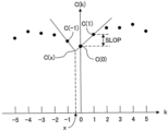
- Figure 4 shows the calculation results of equation (1) when the correlation between the paired image signal strings is high in an ideal state without noise.
- the k at which the discrete correlation amount C(k) is minimum is denoted as kj.
- the pixel shift amount (phase difference) x that gives the minimum value C(x) for continuous correlation amounts is calculated by the three-point interpolation process shown in equations (2) to (4).
- the pixel shift amount x is a real value, and its unit is pixels.
- the SLOP in the formula (4) represents the slope of the change in the correlation amount that is the smallest and the local minimum and the correlation amount adjacent thereto.
- kj 0.
- the pixel shift amount x between the pair of image signal strings is ideally 0.00.
- Figure 5 shows the calculation results when formula (1) is applied to a small block containing noise.
- the effect of randomly distributed noise reduces the correlation between paired image signal sequences.
- the minimum value of the correlation amount C(k) becomes larger than the minimum value shown in Figure 4, and the correlation amount curve becomes generally flat (the absolute value of the difference between the maximum and minimum values becomes smaller).
- the reliability of the calculated pixel shift amount x can be determined by the SLOP value. That is, when the SLOP value is large, it can be determined that the correlation between the pair of image signal strings is high, and when the SLOP value is small, it can be determined that no significant correlation was obtained between the pair of image signal strings.
- the correlation amount C(k) is minimum and extremely small at the shift amount k where the correlation between the pair of image signal strings is highest.
- a correlation calculation method in which the correlation amount C(k) is maximum and extremely large at the shift amount k where the correlation between the pair of image signal strings is highest may be used.
- step S305 the image processing unit 105 calculates the reliability of the calculated pixel shift amount x.
- the reliability can be defined by C(kj), which indicates the degree of match between the pair of image signals calculated in step S304, and the value of SLOP.
- step S306 the image processing unit 105 performs an interpolation process.
- the correlation calculation was successful in step S304, there are cases in which the pixel shift amount x of the pixel of interest cannot be adopted due to low reliability calculated in step S305. In such cases, it is necessary to obtain the pixel shift amount of the pixel of interest by interpolation using the pixel shift amounts calculated for the pixels surrounding the pixel of interest.
- a median filter may be applied to the pixel shift amount calculated for the surrounding pixels, or a method may be used in which the pixel shift amount data is reduced and then enlarged again.
- color data may be extracted from the imaging signal, and the pixel shift amount may be interpolated using the color data.
- step S307 the image processing unit 105 calculates the defocus amount by referring to the pixel shift amount x calculated in step S304 or obtained by interpolation in step S306.
- the defocus amount (DEF) can be calculated by the following formula (5).
- P is a conversion coefficient determined by the detection pitch and the distance between the projection centers of the two viewpoints in the pair of parallax images (A image signal and B image signal) (the distance between the center of gravity of the image sensor that generates the A image signal and the center of gravity of the image sensor that generates the B image signal).
- the unit of the conversion coefficient is mm/pixel.
- step S308 the image processing unit 105 calculates the distance from the defocus amount calculated in step S307.
- the distance to the subject is Da
- the focal position of the lens unit 106 is Db
- the focal length is F
- equation (7) becomes:
- the absolute distance Da' to the subject can be calculated.
- the relative distance Da-Da' is calculated from equations (7) and (8) as follows:
- the pixel shift amount, defocus amount, and distance to the subject can be obtained from the A and B image signals.
- the pixel shift amount and defocus amount obtained in this manner change depending on the distance from the imaging device 100. Therefore, the pixel shift amount, defocus amount, and distance are all information relating to the distance from the imaging device 100.
- information relating to distance is referred to as distance information.
- information relating to distance is not limited to distance itself, but may be information that can be converted into or associated with distance.
- Fig. 7(a) shows how an image of a subject OBJ positioned in front of an LED display LD as a background display is captured by an imaging device 100.
- the LED display LD is configured with a large number of LEDs as display elements arranged in a two-dimensional direction, and displays a background image according to a video signal supplied from a video supply device (not shown).
- the image data obtained by imaging shows the subject OBJ against the background image.
- the imaging device 100 captures an image of the subject OBJ and the LED display LS from a direction different from the direction of the normal N (direction facing the LED display LD), which is a plane.
- the background display is not limited to a plane, and may be curved or spherical. If the angle between the imaging direction of the imaging device 100 and the display surface of the LED display LD is significantly different from 90°, the viewing angle characteristics of the LED display LD will reduce the luminance of the light incident on the imaging device 100 from the LED display LD. As a result, image quality unevenness (luminance unevenness) due to the above angle will occur in the background image area of the image data obtained by the imaging device 100. For this reason, it is desirable to perform luminance value correction on the image data as image processing to reduce this image quality unevenness.
- the flowchart in FIG. 6 shows the process executed by the image processing unit 105 in the imaging device 100 according to a program in the first embodiment.
- step S601 the image processing unit 105 acquires image data as an input image obtained by capturing an image of the object OBJ and the LED display LD, and information on the distance between the object OBJ and the LED display LD, and stores the data in the frame memory 111.
- the image processing unit 105 reads out image data and distance information from the frame memory 111. From the distance information, the image processing unit 105 determines the subject area in which the subject in the image data is captured and the LED display area (background image area) in which the LED display LD is captured, as shown in FIG. 7(b), and separates them. Specifically, a threshold is set for the distance information, and an area in the image data having distance information equal to or greater than the threshold is determined to be an LED display area, and an area in the image data having distance information less than the threshold is determined to be an object area. The threshold may be set arbitrarily by the user through operation of the operation unit 113, or may be set by the CPU 102 according to the aperture value, focus position, etc. of the lens unit 106. The image processing unit 105 adds flags to distinguish between the subject area and the LED display area in the image data, and stores the image data in the frame memory 111.
- step S603 the image processing unit 105 reads the image data and distance information from the frame memory 111. As shown in FIG. 8, the image processing unit 105 divides the image data into a plurality of x blocks in the horizontal direction and a plurality of y blocks in the vertical direction. Each block may be a square or may have another shape.
- the image processing unit 105 calculates the average value of the distance information for each divided block. At this time, the image processing unit 105 refers to the flag added to the image data in step S602, and calculates the average value of the distance information of only the LED display area, and does not include the distance information of the subject area in the calculation of the average value. The image processing unit 105 stores the average value of the distance information for each block in the frame memory 111.
- step S604 the image processing unit 105 reads out from the frame memory 111 the average value of the image data and distance information of the correction target block and the average value of the image data and distance information of the left adjacent block adjacent to the correction target block on the left side.
- the upper left block of all blocks is initially set as the correction target block, and in step S613 described later, the correction target block is moved one by one in the raster direction.
- the image processing unit 105 calculates the angle between the area corresponding to the correction target block on the display surface of the LED display LD and the imaging direction (imaging optical axis) of the imaging device 100 for each correction target block as arrangement information indicating the arrangement relationship between the LED display LD and the imaging device 100.
- the angle referred to here may indicate the angle itself, or may be a value that can be converted to or associated with an angle, and may be information related to the angle.
- the above angle is referred to as the angle between the LED display LD (area corresponding to the block) and the imaging device 100.
- the image processing unit 105 calculates the angle between the imaging device 100 and an area on the LED display LD that corresponds to the left half (adjacent block side) of the block to be corrected, using the average value of the distance information of the block to be corrected and the block adjacent to the left.
- Figure 10(a) shows the positional relationship in the horizontal plane between the imaging device 100 and the LED display.
- vertex A shows the imaging position of the imaging device 100
- vertex B shows the point on the LED display that is captured at the center point of the block to be corrected
- vertex C shows the point on the LED display that is captured at the center point of the adjacent block to the left.
- the distance Lc from vertex A to vertex B and the distance Lb from vertex A to vertex C are known from the average value of the distance information.
- Vertex A is the vertex that connects the center points of two adjacent blocks when image data obtained by imaging at the angle of view of lens unit 106 is divided horizontally into x blocks, and the imaging position of imaging device 100. Therefore, the angle degA of vertex A is the value obtained by dividing the angle of view of lens unit 106 by x.
- image processing unit 105 can calculate the distance La from vertex B to vertex C using the cosine theorem shown in the following equation (10).
- the angle degD between the imaging device 100 and the area on the LED display LD that corresponds to the left half of the block to be corrected can be obtained by averaging the distance information between the center point of the block to be corrected and the center point of the adjacent block to the left.
- Vertex C in FIG. 10(a) and (b) is the point on the LED display that is reflected at the center point of the block to be corrected
- vertex B is the point on the LED display that is reflected at the center point of the adjacent block to the right.
- step S605 the image processing unit 105 multiplies the luminance value of the image data of the left half of the block to be corrected, shown by the diagonal lines in FIG. 9A, by the luminance correction value corresponding to the angle found in step S604.
- a LUT lookup table
- the image processing unit 105 reads out the luminance correction value corresponding to the angle found in step S604 from the LUT.
- the LUT for the luminance correction value stores luminance correction values from angles 0° to 180°, with the luminance correction value being multiplied by 1 when the angle is 90°, and the luminance correction value decreases toward 0 as the angle moves away from 90°.
- This luminance correction value is a value that changes (increases) the luminance value of the image data in the opposite direction to the viewing angle characteristic of the LED display LD, in which the luminance of the LED decreases as the observation position moves away from 90°.
- the image processing unit 105 may calculate and obtain the brightness correction value corresponding to the angle using a formula or the like.
- the image processing unit 105 stores the image data multiplied by the brightness correction value in the frame memory 111.
- step S606 the image processing unit 105 reads out from the frame memory 111 the average value of the image data and distance information of the block to be corrected and the average value of the image data and distance information of the block adjacent to the right of the block to be corrected.
- the image processing unit 105 calculates the angle between the imaging device 100 and an area on the LED display LD that corresponds to the right half of the block to be corrected, using the average values of the distance information of the block to be corrected and the block to the right, as shown in FIG. 9(b).
- step S607 the image processing unit 105 multiplies the luminance value of the image data of the right half of the block to be corrected, shown by the diagonal lines in FIG. 9(b), by the luminance correction value corresponding to the angle determined in step S606.
- the luminance correction value used here is the same as that used in step S605.
- the image processing unit 105 stores the image data multiplied by the luminance correction value in the frame memory 111.
- step S608 the image processing unit 105 reads out from the frame memory 111 the average value of the image data and distance information of the correction target block and the average value of the image data and distance information of the upper neighboring block adjacent to the correction target block on the upper side.
- the image processing unit 105 calculates the angle between the imaging device 100 and an area on the LED display LD that corresponds to the upper half of the correction target block, using the average values of the distance information of the correction target block and the upper neighboring block, as shown in FIG. 9(c).
- step S609 the image processing unit 105 multiplies the luminance value of the image data in the upper half of the block to be corrected, shown by diagonal lines in FIG. 9(c), by a luminance correction value according to the angle found in step S608.
- the luminance correction value may be the same as that used in steps S605 and S607, or, if the vertical viewing angle characteristics of the LED display LD differ from the horizontal direction, a value that corrects the luminance value in the opposite direction to the vertical viewing angle characteristics may be used.
- the image processing unit 105 stores the image data multiplied by the luminance correction value in the frame memory 111.
- step S610 the image processing unit 105 reads out from the frame memory 111 the average value of the image data and distance information of the block to be corrected and the average value of the image data and distance information of the block adjacent to the block to be corrected on the lower side.
- the image processing unit 105 calculates the angle between the imaging device 100 and an area on the LED display LD that corresponds to the lower half of the block to be corrected, using the average values of the distance information of the block to be corrected and the block adjacent to the lower side, as shown in FIG. 9(d).
- step S611 the image processing unit 105 multiplies the luminance value of the image data of the lower half of the block to be corrected, indicated by diagonal lines in FIG. 9(d), by the luminance correction value according to the angle found in step S610.
- the luminance correction value used here is the same as that used in step S609.
- the image processing unit 105 stores the image data multiplied by the luminance correction value in the frame memory 111.
- step S612 the image processing unit 105 determines whether or not the luminance value correction in steps S604 to S611 has been performed for all x horizontal by y vertical blocks, and ends this process if correction has been performed for all blocks. If there are any blocks that have not yet been corrected, the process of step S613 is performed.
- step S613 the image processing unit 105 moves the correction target block in the raster direction. Then, the process returns to step S604.
- the luminance value of the background image area in the image data (input image) can be corrected according to the angle between the LED display LD and the imaging device 100. Therefore, it is possible to obtain image data (output image) in which the image quality unevenness of the background image area is reduced. Moreover, since the emission luminance of the LED display LD itself is not changed, even when imaging is performed simultaneously using multiple imaging devices arranged at different angles, it is possible to obtain image data in which the image quality unevenness of the background image area is reduced in each imaging device.
- the angle between the LED display and the imaging device is calculated using the average value of the distance information for each block, but other distance information, such as distance information for the center position of each block, may be used instead of the average value.
- image quality unevenness caused by the distance between the LED display and the imaging device 100 is corrected, rather than image quality unevenness caused by the angle between the LED display and the imaging device 100.
- step S601 to step S603 show the process executed by the image processing unit 105 in accordance with a program in the second embodiment.
- the processes from step S601 to step S603 are the same as those in the steps with the same reference numerals in the first embodiment (FIG. 6).
- the image processing unit 105 reads out the average value of the distance information for each divided block in the image data (input image) from the frame memory 111. At this time, the image processing unit 105 normalizes the average value of the distance information for each block by setting the average value of the distance information for all blocks to 1. The image processing unit 105 stores the normalized average value of the distance information for each block in the frame memory 111 as the arrangement information of the LED display LD and the imaging device 100.
- the image processing unit 105 reads out the image data of the correction target block and the average value of the normalized distance information from the frame memory 111.
- the image processing unit 105 calculates a luminance correction value from the average value of the normalized distance information. In other words, it calculates a luminance correction value according to the distance.
- the luminance of the image data is inversely proportional to the square of the distance between the LED display and the imaging device 100. For this reason, the image processing unit 105 sets the luminance correction value according to the distance to the reciprocal of the value obtained by squaring the average value of the normalized distance information.
- step S1103 the image processing unit 105 multiplies the luminance value of the image data of the correction target block by a luminance correction value according to the distance calculated in step S1102.
- the image processing unit 105 stores the image data multiplied by the luminance correction value in the frame memory 111.
- step S1104 the image processing unit 105 determines whether or not the luminance value correction in steps S1102 and S1103 has been performed for all x horizontal by y vertical blocks, and ends this process if correction has been performed for all blocks. If there are any blocks that have not yet been corrected, the process of step S613 is performed.
- the process of step S613 is the same as the process of the step of the same symbol in Example 1 ( Figure 6), but in this example, the process returns to step S1102.
- the LED display is configured with LEDs of multiple colors, for example, three colors R (red), G (green), and B (blue), it is desirable to prepare brightness correction values for the angle or distance for each of the R, G, and B colors of the image data, and perform brightness value correction for each color.
- a map of luminance correction values for all blocks may be created, and luminance value correction may be performed using the luminance correction value obtained by performing two-dimensional filtering processing such as low-pass filtering on this map.
- the distance information is not limited to the process shown in FIG. 3 using the image sensor, but may be obtained using a distance measuring device that is provided in the image sensor 100 separately from the image sensor and that is capable of measuring the distance to the subject.
- distance measuring devices include radar and LiDAR (Light Detection and Ranging).
- an LED display was used as the background display.
- this is not limited to LED displays.
- the brightness value can be corrected according to at least one of the angle and distance.
- the image processing unit 105 performs image processing to correct the brightness value of the image data according to the angle and distance between the background display LD and the imaging device 100.
- image processing may be performed.
- the background display LD is a VA (Vertical Alignment) panel or the like
- VA Very Alignment
- the image processing unit 105 may also add the above-mentioned map of brightness correction values as metadata to image data serving as an input image, and output this image data to the outside from output units such as the network module 108, the video terminal 109, and the recording medium 112. This allows an external device to perform brightness value correction of the image data by referring to the map of brightness correction values.
- the image processing unit 105 as an information processing device is built into the imaging device 100.
- a personal computer having the same functions as the image processing unit 105 (operating according to a program that realizes the same functions) may be provided as an information processing device separate from the imaging device.
- the present invention can also be realized by a process in which a program for implementing one or more of the functions of the above-described embodiments is supplied to a system or device via a network or a storage medium, and one or more processors in a computer of the system or device read and execute the program.
- the present invention can also be realized by a circuit (e.g., ASIC) that implements one or more of the functions.
Landscapes
- Engineering & Computer Science (AREA)
- Multimedia (AREA)
- Signal Processing (AREA)
- Computer Vision & Pattern Recognition (AREA)
- Physics & Mathematics (AREA)
- General Physics & Mathematics (AREA)
- Theoretical Computer Science (AREA)
- Studio Devices (AREA)
- Image Processing (AREA)
Abstract
Description


C(kj)=C(0)=1000
C(kj-1)=C(-1)=1700
C(kj+1)=C(1)=1830
とする。この例では、kj=0である。式(2)~(4)より、
SLOP=830
x=-0.078pixel
となる。合焦状態では、対の像信号列の画素ずれ量xは0.00が理想値である。
C(kj)=C(0)=1300
C(kj-1)=C(-1)=1480
C(kj+1)=C(1)=1800
とする。この例では、kj=0である。式(2)~(4)より、
SLOP=500
x=-0.32pixel
となる。



本発明は、上述の実施形態の1以上の機能を実現するプログラムを、ネットワーク又は記憶媒体を介してシステム又は装置に供給し、そのシステム又は装置のコンピュータにおける1つ以上のプロセッサーがプログラムを読出し実行する処理でも実現可能である。また、1以上の機能を実現する回路(例えば、ASIC)によっても実現可能である。
Claims (14)
- 撮像装置により被写体と背景ディスプレイに表示された背景映像とを撮像して得られる入力画像を取得する取得手段と、
前記入力画像における被写体領域と背景映像領域とを判別する判別手段と、
前記背景ディスプレイと前記撮像装置との間の角度および距離のうち少なくとも一方に関する配置情報を取得し、前記背景映像領域に対して前記配置情報に応じた画像処理を行う処理手段とを有することを特徴とする情報処理装置。 - 前記画像処理は、前記背景映像領域の輝度値を変更する処理であることを特徴とする請求項1に記載の情報処理装置。
- 前記画像処理は、前記角度および前記距離のうち少なくとも一方に応じて前記背景ディスプレイから前記撮像装置への入射光の輝度が変化する場合に、該入射光の輝度の変化とは逆方向に前記背景映像領域の輝度値を変更する処理であることを特徴とする請求項2に記載の情報処理装置。
- 前記処理手段は、前記配置情報に対応する画像処理用パラメータを予め保持または算出し、該画像処理用パラメータを用いて前記画像処理を行うことを特徴とする請求項1から3のいずれか一項に記載の情報処理装置。
- 前記判別手段は、
前記撮像装置から前記被写体および前記背景ディスプレイまでの距離に関する情報を用いて前記被写体領域と前記背景映像領域とを判別することを特徴とする請求項1から4のいずれか一項に記載の情報処理装置。 - 前記処理手段は、
前記背景映像領域を複数のブロックに分割し、
前記ブロックごとに前記配置情報を取得して前記画像処理を行うことを特徴とする請求項1から5のいずれか一項に記載の情報処理装置。 - 前記処理手段は、
前記複数のブロックのうち対象ブロックと該対象ブロックに対する隣接ブロックのそれぞれの前記配置情報を取得し、
前記対象ブロックと前記隣接ブロックの前記配置情報に応じて、前記対象ブロックにおける前記隣接ブロック側の部分に対して前記画像処理を行うことを特徴とする請求項6に記載の情報処理装置。 - 前記処理手段は、前記撮像装置から前記背景ディスプレイのまでの距離に関する情報を用いて前記角度に関する情報を取得することを特徴とする請求項1から7のいずれか一項に記載の情報処理装置。
- 前記背景映像が複数の色を有する場合に、前記入力画像に対して前記色ごとに前記画像処理を行うことを特徴とする請求項1から8のいずれか一項に記載の情報処理装置。
- 前記処理手段は、前記配置情報に対応する画像処理用パラメータを前記入力画像に付加して外部に出力することを特徴とする請求項1から9のいずれか一項に記載の情報処理装置。
- 前記撮像装置に設けられた撮像素子の複数の画素はそれぞれ、前記光学系の瞳のうち互いに異なる領域からの光を受光する複数の光電変換素子を有し、
前記処理手段は、前記複数の画素の前記複数の光電変換素子から出力された信号を用いて生成された対の像信号の位相差から前記配置情報を取得することを特徴とする請求項1から10のいずれか一項に記載の情報処理装置。 - 請求項1から11のいずれか一項に記載の情報処理装置と、
撮像素子とを有することを特徴とする撮像装置。 - 撮像装置により被写体と背景ディスプレイに表示された背景映像とを撮像して得られる入力画像を取得するステップと、
前記入力画像における被写体領域と背景映像領域とを判別するステップと、
前記背景ディスプレイと前記撮像装置との間の角度および距離のうち少なくとも一方に関する配置情報を取得し、前記背景映像領域に対して前記配置情報に応じた画像処理を行うステップとを有することを特徴とする情報処理方法。 - コンピュータに、請求項13に記載の情報処理方法に従う処理を実行させることを特徴とするプログラム。
Priority Applications (3)
| Application Number | Priority Date | Filing Date | Title |
|---|---|---|---|
| EP24810710.4A EP4723659A1 (en) | 2023-05-25 | 2024-03-28 | Information processing device and imaging device |
| CN202480034250.9A CN121195512A (zh) | 2023-05-25 | 2024-03-28 | 信息处理设备和摄像设备 |
| US19/387,997 US20260075325A1 (en) | 2023-05-25 | 2025-11-13 | Information processing apparatus and image pickup apparatus |
Applications Claiming Priority (2)
| Application Number | Priority Date | Filing Date | Title |
|---|---|---|---|
| JP2023-085973 | 2023-05-25 | ||
| JP2023085973A JP2024168917A (ja) | 2023-05-25 | 2023-05-25 | 情報処理装置および撮像装置 |
Related Child Applications (1)
| Application Number | Title | Priority Date | Filing Date |
|---|---|---|---|
| US19/387,997 Continuation US20260075325A1 (en) | 2023-05-25 | 2025-11-13 | Information processing apparatus and image pickup apparatus |
Publications (1)
| Publication Number | Publication Date |
|---|---|
| WO2024241702A1 true WO2024241702A1 (ja) | 2024-11-28 |
Family
ID=93590107
Family Applications (1)
| Application Number | Title | Priority Date | Filing Date |
|---|---|---|---|
| PCT/JP2024/012563 Ceased WO2024241702A1 (ja) | 2023-05-25 | 2024-03-28 | 情報処理装置および撮像装置 |
Country Status (5)
| Country | Link |
|---|---|
| US (1) | US20260075325A1 (ja) |
| EP (1) | EP4723659A1 (ja) |
| JP (1) | JP2024168917A (ja) |
| CN (1) | CN121195512A (ja) |
| WO (1) | WO2024241702A1 (ja) |
Families Citing this family (1)
| Publication number | Priority date | Publication date | Assignee | Title |
|---|---|---|---|---|
| JP2026060391A (ja) | 2024-09-27 | 2026-04-08 | セイコーエプソン株式会社 | 液体吐出装置、及び容量性負荷駆動回路 |
Citations (7)
| Publication number | Priority date | Publication date | Assignee | Title |
|---|---|---|---|---|
| JP2010067223A (ja) * | 2008-09-12 | 2010-03-25 | Canon Inc | 画像処理装置、画像処理方法、及び、画像処理プログラム |
| JP2011028177A (ja) * | 2009-07-29 | 2011-02-10 | Nikon Corp | 撮像装置 |
| WO2014119257A1 (ja) * | 2013-01-29 | 2014-08-07 | パナソニック株式会社 | 撮像システム |
| JP2015033020A (ja) * | 2013-08-02 | 2015-02-16 | キヤノン株式会社 | 撮像装置、撮像方法、プログラム、及び記録媒体 |
| US20170150067A1 (en) * | 2015-11-24 | 2017-05-25 | Samsung Electronics Co., Ltd. | Digital photographing apparatus and method of operating the same |
| US20220014728A1 (en) | 2020-07-13 | 2022-01-13 | Brompton Technology Ltd. | System and Method for Realtime LED Viewing Angle Correction |
| JP2022140057A (ja) * | 2021-03-12 | 2022-09-26 | キヤノン株式会社 | 画像処理装置、画像処理方法、及びプログラム |
-
2023
- 2023-05-25 JP JP2023085973A patent/JP2024168917A/ja active Pending
-
2024
- 2024-03-28 CN CN202480034250.9A patent/CN121195512A/zh active Pending
- 2024-03-28 EP EP24810710.4A patent/EP4723659A1/en active Pending
- 2024-03-28 WO PCT/JP2024/012563 patent/WO2024241702A1/ja not_active Ceased
-
2025
- 2025-11-13 US US19/387,997 patent/US20260075325A1/en active Pending
Patent Citations (7)
| Publication number | Priority date | Publication date | Assignee | Title |
|---|---|---|---|---|
| JP2010067223A (ja) * | 2008-09-12 | 2010-03-25 | Canon Inc | 画像処理装置、画像処理方法、及び、画像処理プログラム |
| JP2011028177A (ja) * | 2009-07-29 | 2011-02-10 | Nikon Corp | 撮像装置 |
| WO2014119257A1 (ja) * | 2013-01-29 | 2014-08-07 | パナソニック株式会社 | 撮像システム |
| JP2015033020A (ja) * | 2013-08-02 | 2015-02-16 | キヤノン株式会社 | 撮像装置、撮像方法、プログラム、及び記録媒体 |
| US20170150067A1 (en) * | 2015-11-24 | 2017-05-25 | Samsung Electronics Co., Ltd. | Digital photographing apparatus and method of operating the same |
| US20220014728A1 (en) | 2020-07-13 | 2022-01-13 | Brompton Technology Ltd. | System and Method for Realtime LED Viewing Angle Correction |
| JP2022140057A (ja) * | 2021-03-12 | 2022-09-26 | キヤノン株式会社 | 画像処理装置、画像処理方法、及びプログラム |
Also Published As
| Publication number | Publication date |
|---|---|
| EP4723659A1 (en) | 2026-04-08 |
| CN121195512A (zh) | 2025-12-23 |
| US20260075325A1 (en) | 2026-03-12 |
| JP2024168917A (ja) | 2024-12-05 |
Similar Documents
| Publication | Publication Date | Title |
|---|---|---|
| JP5640143B2 (ja) | 撮像装置及び撮像方法 | |
| CN102812714B (zh) | 立体图像获取装置 | |
| JP4699995B2 (ja) | 複眼撮像装置及び撮像方法 | |
| CN105872525B (zh) | 图像处理装置和图像处理方法 | |
| US8786676B2 (en) | Imaging device for generating stereoscopic image | |
| CN103039066B (zh) | 成像装置、图像处理装置以及图像处理方法 | |
| JP2014039125A (ja) | 画像処理装置、画像処理装置を具備する撮像装置、画像処理方法、及びプログラム | |
| CN102884802A (zh) | 三维成像装置和视点图像恢复方法 | |
| WO2012036019A1 (ja) | 単眼立体撮像装置、単眼立体撮像装置用シェーディング補正方法及び単眼立体撮像装置用プログラム | |
| WO2012108099A1 (ja) | 撮像装置および撮像方法 | |
| US10122990B2 (en) | Imaging system and method of producing context and focus images | |
| US20260075325A1 (en) | Information processing apparatus and image pickup apparatus | |
| TWI599809B (zh) | 鏡頭模組陣列、影像感測裝置與數位縮放影像融合方法 | |
| JP2011211329A (ja) | 撮像装置およびその制御方法,ならびに画像処理装置,その制御方法,および画像処理プログラム | |
| WO2019181560A1 (ja) | 画像処理装置、撮像装置、画像処理方法、プログラム | |
| JP2009047734A (ja) | 撮像装置及び画像処理プログラム | |
| US12273630B2 (en) | Image processing apparatus, image processing method, and storage medium | |
| JP2012124650A (ja) | 撮像装置および撮像方法 | |
| JP5453328B2 (ja) | 立体撮像システム、補正装置およびそのプログラム | |
| JPWO2016076396A1 (ja) | 撮像装置および撮像方法 | |
| JP2024175256A (ja) | 情報処理装置および撮像装置 | |
| JP2024168751A (ja) | 情報処理装置および撮像装置 | |
| JP5399986B2 (ja) | 撮像装置、画像処理方法 | |
| JP2011182325A (ja) | 撮像装置 | |
| JP2024060961A (ja) | 画像処理装置、撮像装置、制御方法及びプログラム |
Legal Events
| Date | Code | Title | Description |
|---|---|---|---|
| 121 | Ep: the epo has been informed by wipo that ep was designated in this application |
Ref document number: 24810710 Country of ref document: EP Kind code of ref document: A1 |
|
| NENP | Non-entry into the national phase |
Ref country code: DE |
|
| WWE | Wipo information: entry into national phase |
Ref document number: 2024810710 Country of ref document: EP |
|
| ENP | Entry into the national phase |
Ref document number: 2024810710 Country of ref document: EP Effective date: 20260102 |
|
| ENP | Entry into the national phase |
Ref document number: 2024810710 Country of ref document: EP Effective date: 20260102 |
|
| ENP | Entry into the national phase |
Ref document number: 2024810710 Country of ref document: EP Effective date: 20260102 |
|
| ENP | Entry into the national phase |
Ref document number: 2024810710 Country of ref document: EP Effective date: 20260102 |
|
| ENP | Entry into the national phase |
Ref document number: 2024810710 Country of ref document: EP Effective date: 20260102 |
|
| ENP | Entry into the national phase |
Ref document number: 2024810710 Country of ref document: EP Effective date: 20260102 |
|
| WWP | Wipo information: published in national office |
Ref document number: 2024810710 Country of ref document: EP |