WO2024252605A1 - 半導体装置 - Google Patents
半導体装置 Download PDFInfo
- Publication number
- WO2024252605A1 WO2024252605A1 PCT/JP2023/021307 JP2023021307W WO2024252605A1 WO 2024252605 A1 WO2024252605 A1 WO 2024252605A1 JP 2023021307 W JP2023021307 W JP 2023021307W WO 2024252605 A1 WO2024252605 A1 WO 2024252605A1
- Authority
- WO
- WIPO (PCT)
- Prior art keywords
- electrode
- sealing material
- semiconductor device
- bus bar
- semiconductor element
- Prior art date
- Legal status (The legal status is an assumption and is not a legal conclusion. Google has not performed a legal analysis and makes no representation as to the accuracy of the status listed.)
- Ceased
Links
Images




Classifications
-
- H—ELECTRICITY
- H10—SEMICONDUCTOR DEVICES; ELECTRIC SOLID-STATE DEVICES NOT OTHERWISE PROVIDED FOR
- H10W—GENERIC PACKAGES, INTERCONNECTIONS, CONNECTORS OR OTHER CONSTRUCTIONAL DETAILS OF DEVICES COVERED BY CLASS H10
- H10W90/00—Package configurations
-
- H—ELECTRICITY
- H10—SEMICONDUCTOR DEVICES; ELECTRIC SOLID-STATE DEVICES NOT OTHERWISE PROVIDED FOR
- H10W—GENERIC PACKAGES, INTERCONNECTIONS, CONNECTORS OR OTHER CONSTRUCTIONAL DETAILS OF DEVICES COVERED BY CLASS H10
- H10W74/00—Encapsulations, e.g. protective coatings
- H10W74/10—Encapsulations, e.g. protective coatings characterised by their shape or disposition
- H10W74/111—Encapsulations, e.g. protective coatings characterised by their shape or disposition the semiconductor body being completely enclosed
Definitions
- This disclosure relates to a semiconductor device.
- semiconductor devices are required to have high heat dissipation properties.
- the main terminals and control terminals are exposed from the upper flush surface of the sealing resin body to improve heat dissipation properties.
- Semiconductor devices are required to have not only high heat dissipation but also low inductance to reduce losses. Reducing the distance between electrodes is an effective way to reduce inductance, but when the distance between electrodes is reduced, issues arise in ensuring insulation between the electrodes.
- This disclosure has been made to solve the problems described above, and aims to provide a semiconductor device that achieves high insulation and low inductance.
- the semiconductor device includes a semiconductor element, a first electrode, a second electrode, and a sealing material.
- the first electrode is electrically connected to the semiconductor element.
- the second electrode is provided adjacent to the first electrode and is electrically connected to the semiconductor element.
- the sealing material seals the semiconductor element, all except the top surface of the first electrode, and all except the top surface of the second electrode.
- the first electrode includes a first side surface and a first top surface. The first side surface protrudes from the outer peripheral top surface that constitutes the outer periphery of the sealing material and faces the second electrode. The first top surface is exposed from the sealing material.
- the second electrode includes a second side surface and a second top surface.
- the second side surface protrudes from the outer peripheral top surface that constitutes the outer periphery of the sealing material and faces the first electrode.
- the second top surface is exposed from the sealing material.
- the first side surface and the second side surface are covered with the sealing material.
- the sealing material includes at least one of a recess and a protrusion between the first electrode and the second electrode.
- This disclosure provides a semiconductor device that achieves high insulation and low inductance.
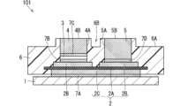
- FIG. 1 is a cross-sectional view showing a configuration of a semiconductor device in a first embodiment.
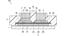
- 11 is a cross-sectional view showing a configuration of a semiconductor device in a second embodiment.
- 11 is a cross-sectional view showing a configuration of a semiconductor device in a third embodiment.
- 13 is a cross-sectional view showing a configuration of a semiconductor device in a fourth embodiment.
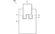
- FIG. 23 is a plan view showing a configuration of a semiconductor device in a sixth embodiment.
- FIG. 23 is a plan view showing a configuration of a semiconductor device in a seventh embodiment.
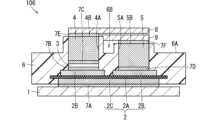
- FIG. 23 is a cross-sectional view showing a configuration of a semiconductor device in a seventh embodiment.
- FIG. 1 is a cross-sectional view showing a configuration of a semiconductor device 101 according to the first embodiment.
- the semiconductor device 101 includes a heat dissipation substrate 1, an insulating substrate 2, a semiconductor element 3, a first electrode 4, a second electrode 5, and a sealing material 6.
- the heat dissipation substrate 1 is a plate made of a metal such as copper or aluminum.
- the heat dissipation substrate 1 has the function of transferring heat generated by electronic components such as semiconductor elements 3 to the outside.
- the insulating substrate 2 is provided on the heat dissipation substrate 1.
- the insulating substrate 2 includes an insulating layer 2A, a front circuit pattern 2B, and a rear circuit pattern 2C.
- the insulating layer 2A is formed of, for example, ceramic.
- the front circuit pattern 2B is provided on the upper surface of the insulating layer 2A.
- the rear circuit pattern 2C is provided on the lower surface of the insulating layer 2A.
- the front circuit pattern 2B and the rear circuit pattern 2C are formed of a conductive material such as metal.
- the rear circuit pattern 2C is bonded to the heat dissipation substrate 1 via a bonding material 7A.
- the bonding material 7A is, for example, solder, brazing material, sintered material, etc.
- the semiconductor element 3 is held by the insulating substrate 2.
- the semiconductor element 3 in the first embodiment is a vertical semiconductor element in which a current flows between its upper surface and lower surface, and includes a front electrode (not shown) and a back electrode (not shown).
- the back electrode of the semiconductor element 3 is bonded to the front circuit pattern 2B of the insulating substrate 2 via a bonding material 7B.
- the bonding material 7B is a conductive material such as solder.
- the semiconductor element 3 is formed of a semiconductor such as Si.
- the semiconductor element 3 is preferably formed of a so-called wide band gap semiconductor such as SiC, GaN, Ga 2 O 3 , or diamond.
- the semiconductor element 3 is a power semiconductor element, a control IC (Integrated Circuit) for controlling the power semiconductor element, or the like.
- the semiconductor element 3 includes, for example, an IGBT (Insulated Gate Bipolar Transistor), a MOSFET (Metal Oxide Semiconductor Field Effect Transistor), a Schottky barrier diode, or the like.
- the semiconductor element 3 may include an RC-IGBT (Reverse-Conducting IGBT) in which an IGBT and a freewheeling diode are formed within a single semiconductor substrate.
- the first electrode 4 is disposed adjacent to the second electrode 5.
- the first electrode 4 is electrically connected to the semiconductor element 3 inside the sealing material 6.
- the lower surface of the first electrode 4 is bonded to the surface electrode of the semiconductor element 3 via the bonding material 7C.
- the surface electrode of the semiconductor element 3 is, for example, an emitter electrode.
- the first electrode 4 protrudes above the outer peripheral upper surface 6A that constitutes the outer periphery of the sealing material 6.
- the first electrode 4 includes a first side surface 4A and a first upper surface 4B.
- the first side surface 4A protrudes from the outer peripheral upper surface 6A of the sealing material 6 and faces the second electrode 5.
- the first side surface 4A is covered with the sealing material 6.
- the entire surface of the first side surface 4A is covered with the sealing material 6.
- the first upper surface 4B is not covered with the sealing material 6 and is exposed from an opening provided in the sealing material 6.
- the shape of the first electrode 4 is not important.
- the first electrode 4 has, for example, a block shape.
- the block shape can be, for example, a square prism, a cylinder, or a U-shape.
- the second electrode 5 is disposed adjacent to the first electrode 4.
- the second electrode 5 is electrically connected to the semiconductor element 3 inside the sealing material 6.
- the lower surface of the second electrode 5 is bonded to the front circuit pattern 2B via a bonding material 7D.
- the front circuit pattern 2B is electrically connected to, for example, a collector electrode, which is a back electrode of the semiconductor element 3.
- the front circuit pattern 2B may be electrically connected to a control electrode such as a gate electrode or a sensing electrode of the semiconductor element 3.
- the second electrode 5 protrudes above the outer peripheral upper surface 6A that constitutes the outer periphery of the sealing material 6.
- the second electrode 5 includes a second side surface 5A and a second upper surface 5B.
- the second side surface 5A protrudes from the outer peripheral upper surface 6A of the sealing material 6 and faces the first electrode 4.
- the second side surface 5A is covered with the sealing material 6.
- the entire surface of the second side surface 5A is covered with the sealing material 6.
- the second upper surface 5B is not covered by the sealing material 6, and is exposed from an opening provided in the sealing material 6.
- the shape of the second electrode 5 is not important.
- the second electrode 5 has, for example, a block shape.
- the block shape has, for example, a rectangular prism, a cylinder, a U-shape, etc.
- the sealing material 6 seals the insulating substrate 2, the semiconductor element 3, and all except the top surface of the first electrode 4 and all except the top surface of the second electrode 5.
- the sealing material 6 in the first embodiment includes a recess 6B between the first electrode 4 and the second electrode 5.
- the bottom surface of the recess 6B is located lower than the first top surface 4B of the first electrode 4 and the second top surface 5B of the second electrode 5.
- the sealing material 6 is made of a resin having insulating properties.
- the sealing material 6 is, for example, a silicone resin, an epoxy resin, or the like.
- the semiconductor device 101 in the first embodiment includes a semiconductor element 3, a first electrode 4, a second electrode 5, and a sealing material 6.
- the first electrode 4 is electrically connected to the semiconductor element 3.
- the second electrode 5 is provided adjacent to the first electrode 4 and is electrically connected to the semiconductor element 3.
- the sealing material 6 seals the semiconductor element 3, the first electrode 4, and the second electrode 5 except for their upper surfaces.
- the first electrode 4 includes a first side surface 4A and a first upper surface 4B.
- the first side surface 4A protrudes from the outer peripheral upper surface 6A that constitutes the outer periphery of the sealing material 6 and faces the second electrode 5.
- the first upper surface 4B is exposed from the sealing material 6.
- the second electrode 5 includes a second side surface 5A and a second upper surface 5B.
- the second side surface 5A protrudes from the outer peripheral upper surface 6A that constitutes the outer periphery of the sealing material 6 and faces the first electrode 4.
- the second upper surface 5B is exposed from the sealing material 6.
- the first side surface 4A and the second side surface 5A are covered with a sealing material 6.
- the sealing material 6 includes at least one of a recess 6B and a protrusion 6C (see Figures 2 and 3) between the first electrode 4 and the second electrode 5.
- the creepage distance between the first electrode 4 and the second electrode 5 is longer than the spatial distance between the first electrode 4 and the second electrode 5.
- the creepage distance corresponds to, for example, the distance from the end of the first upper surface 4B to the end of the second upper surface 5B via the surface of the sealing material 6.
- the spatial distance corresponds to, for example, the linear distance from the end of the first upper surface 4B to the end of the second upper surface 5B. Since the creepage distance is longer than the spatial distance, insulation is ensured even if the spatial distance is reduced. By reducing the spatial distance, the inductances cancel each other out, and the inductance of the semiconductor device 101 decreases. As described above, the semiconductor device 101 achieves high insulation and low inductance.
- the semiconductor device 101 can be applied to various products such as power sources and power sources, power systems, etc.
- the heat dissipation substrate 1 includes an insulating layer 2A formed on the upper surface of the heat dissipation substrate 1 and a front circuit pattern 2B formed on the insulating layer 2A. In this case, no bonding material exists between the insulating layer 2A and the heat dissipation substrate 1.
- the insulating layer 2A is formed of, for example, resin.
- FIG. 2 is a cross-sectional view showing the configuration of a semiconductor device 102 in the second embodiment.
- the sealing material 6 includes a protrusion 6C between the first electrode 4 and the second electrode 5.
- the protrusion 6C in the second embodiment is the sealing material 6 between the first electrode 4 and the second electrode 5 protruding upward.
- the upper surface of the protrusion 6C is located at a higher position than the first upper surface 4B of the first electrode 4 and the second upper surface 5B of the second electrode 5.
- Such a semiconductor device 102 achieves low inductance by reducing the spatial distance between the first electrode 4 and the second electrode 5, and improves insulation by increasing the creepage distance.
- the sealing material 6 includes a recess 6B and a protrusion 6C between the first electrode 4 and the second electrode 5.
- the protrusion 6C of the sealing material 6 includes a first protrusion 16C and a second protrusion 26C.
- the first protrusion 16C covers the first side surface 4A and protrudes above the first upper surface 4B.
- the second protrusion 26C covers the second side surface 5A and protrudes above the second upper surface 5B.
- only the first protrusion 16C and the second protrusion 26C protrude above the first electrode 4 and the second electrode 5.
- the recess 6B of the sealing material 6 is provided between the first protrusion 16C and the second protrusion 26C.
- the bottom surface of the recess 6B is provided at a lower position than the first upper surface 4B of the first electrode 4 and the second upper surface 5B of the second electrode 5.
- Such a semiconductor device 103 achieves low inductance by reducing the spatial distance between the first electrode 4 and the second electrode 5, and improves insulation by increasing the creepage distance.
- the fourth embodiment 4 is a cross-sectional view showing the configuration of a semiconductor device 104 in the fourth embodiment.
- the first electrode 4 and the second electrode 5 are formed of a plate material having multiple bent portions inside the sealing material 6.
- the inter-electrode distance H between the first electrode 4 and the second electrode 5 inside the sealing material 6 is shorter than the distance G between the end of the first upper surface 4B and the end of the second upper surface 5B.
- the inter-electrode distance H in the fourth embodiment is the shortest distance between the first electrode 4 and the second electrode 5 inside the sealing material 6.
- the distance G in the fourth embodiment is the shortest distance between the end of the first upper surface 4B and the end of the second upper surface 5B.
- the sealing material 6 includes a recess 6B between the first electrode 4 and the second electrode 5. The bottom surface of the recess 6B is located lower than the first upper surface 4B and the second upper surface 5B.
- Such a semiconductor device 104 achieves low inductance by reducing the spatial distance between the first electrode 4 and the second electrode 5, and improves insulation by increasing the creepage distance.
- FIG. 5 is a cross-sectional view showing the configuration of a semiconductor device 105 in embodiment 5.
- the sealing material 6 includes a first sealing material 16 and a second sealing material 26.
- the first sealing material 16 seals the insulating substrate 2, the semiconductor element 3, the lower part of the first electrode 4, and the lower part of the second electrode 5.
- the second sealing material 26 covers the first side surface 4A of the first electrode 4 and the second side surface 5A of the second electrode 5.
- the second sealing material 26 is a resin having insulating properties.
- the second sealing material 26 is, for example, an epoxy resin.
- Such a semiconductor device 105 achieves low inductance by reducing the spatial distance between the first electrode 4 and the second electrode 5, and improves insulation by increasing the creepage distance.
- FIG. 6 is a plan view showing the configuration of a semiconductor device 106 in the sixth embodiment.
- FIG. 7 is a cross-sectional view showing the configuration of a semiconductor device 106 in the sixth embodiment.
- the semiconductor device 106 includes a first bus bar 8 and a second bus bar 9.
- the height of the first top surface 4B from the outer peripheral top surface 6A of the sealing material 6 is different from the height of the second top surface 5B from the outer peripheral top surface 6A of the sealing material 6.
- the first top surface 4B is located at a higher position than the second top surface 5B.
- the first side surface 4A and the second side surface 5A are covered with the sealing material 6.
- the sealing material 6 includes a recess 6B between the first electrode 4 and the second electrode 5.
- the first busbar 8 has a flat plate shape.
- the first busbar 8 is joined to the first upper surface 4B of the first electrode 4 via a bonding material 7E.
- the second busbar 9 has a flat plate shape.
- the second busbar 9 is joined to the second upper surface 5B of the second electrode 5 via a bonding material 7F.
- the first busbar 8 and the second busbar 9 are arranged parallel to each other and overlap with a gap therebetween.
- the first busbar 8 and the second busbar 9 in the sixth embodiment are parallel flat plates.
- the first busbar 8 and the second busbar 9 are connected to a power system outside the semiconductor device 106.
- first bus bar 8 and the second bus bar 9 can be parallel plates, the clearance between the first bus bar 8 and the second bus bar 9 can be designed with high precision. Since the first bus bar 8 and the second bus bar 9 are parallel plates, the inductance of the entire power system including the semiconductor device 106 is reduced.
- first bus bar 8 and the second bus bar 9 which are parallel plates as described above, are effective.
- the sealing material 6 shown in FIG. 7 may have a protrusion in addition to the recess 6B.
- the protrusion is provided inside the recess 6B.
- the height of the protrusion is such that it does not come into contact with the first bus bar 8 and the second bus bar 9. Unlike what is shown in FIG. 7, if the area between the first electrode 4 and the second electrode 5 is not covered by the first bus bar 8 and the second bus bar 9, the height of the protrusion may be higher than at least one of the first upper surface 4B and the second upper surface 5B.
- FIG. 8 is a plan view showing the configuration of semiconductor device 107 in embodiment 7.
- FIG. 9 is a cross-sectional view showing the configuration of semiconductor device 107 in embodiment 7.
- the basic configuration of semiconductor device 107 is similar to that of semiconductor device 106 shown in embodiment 6.
- first bus bar 8 has weld marks 8A.
- the weld marks 8A are formed at the joint between first bus bar 8 and first upper surface 4B of first electrode 4.
- second bus bar 9 has weld marks 8B.
- the weld marks 8B are formed at the joint between second bus bar 9 and second upper surface 5B of second electrode 5.
- the volume of the bonding material differs before and after hardening. This makes it difficult to control the clearance between the first busbar 8 and the second busbar 9.
- the clearance between the first busbar 8 and the second busbar 9 can be controlled with high precision.
Landscapes
- Structures Or Materials For Encapsulating Or Coating Semiconductor Devices Or Solid State Devices (AREA)
Abstract
高い絶縁性および低いインダクタンスを実現する半導体装置を提供する。半導体装置は、半導体素子、第1電極、第2電極および封止材を含む。第1電極は、半導体素子に電気的に接続されている。第2電極は、第1電極と隣り合うように設けられ、半導体素子に電気的に接続されている。封止材は、半導体素子、第1電極の上面以外および第2電極の上面以外を封止している。第1電極は、第1側面および第1上面を含む。第1側面は、封止材の外周部を構成する外周上面から突出しかつ第2電極と向かい合っている。第1上面は、封止材から露出している。第2電極は、第2側面および第2上面を含む。第2側面は、封止材の外周部を構成する外周上面から突出しかつ第1電極と向かい合っている。第2上面は、封止材から露出している。第1側面と第2側面とは、封止材で覆われている。封止材は、第1電極と第2電極との間に凹部および凸部のうち少なくとも一方を含む。
Description
本開示は、半導体装置に関する。
半導体装置には、高い放熱性が求められる。特許文献1に記載の半導体装置においては、放熱性の向上のため、主端子および制御端子が封止樹脂体の上部の面一の面から露出している。
半導体装置には、高放熱化だけでなく、損失低減のための低インダクタンス化も求められている。低インダクタンス化には電極間の距離の縮小化が効果的であるが、電極間の距離が縮小化された場合、電極間の絶縁性の確保に課題が生じる。
本開示は上記のような問題を解決するためになされたものであり、高い絶縁性および低いインダクタンスを実現する半導体装置の提供を目的とする。
本開示に係る半導体装置は、半導体素子、第1電極、第2電極および封止材を含む。第1電極は、半導体素子に電気的に接続されている。第2電極は、第1電極と隣り合うように設けられ、半導体素子に電気的に接続されている。封止材は、半導体素子、第1電極の上面以外および第2電極の上面以外を封止している。第1電極は、第1側面および第1上面を含む。第1側面は、封止材の外周部を構成する外周上面から突出しかつ第2電極と向かい合っている。第1上面は、封止材から露出している。第2電極は、第2側面および第2上面を含む。第2側面は、封止材の外周部を構成する外周上面から突出しかつ第1電極と向かい合っている。第2上面は、封止材から露出している。第1側面と第2側面とは、封止材で覆われている。封止材は、第1電極と第2電極との間に凹部および凸部のうち少なくとも一方を含む。
本開示によれば、高い絶縁性および低いインダクタンスを実現する半導体装置が提供される。
本開示の目的、特徴、局面、および利点は、以下の詳細な説明と添付図面とによって、より明白になる。
<実施の形態1>
図1は、実施の形態1における半導体装置101の構成を示す断面図である。
図1は、実施の形態1における半導体装置101の構成を示す断面図である。
半導体装置101は、放熱基板1、絶縁基板2、半導体素子3、第1電極4、第2電極5および封止材6を含む。
放熱基板1は、例えば銅、アルミニウム等の金属で形成された板である。放熱基板1は、半導体素子3等の電子部品で発生した熱を外部に伝える機能を有する。
絶縁基板2は、放熱基板1上に設けられている。絶縁基板2は、絶縁層2A、表回路パターン2Bおよび裏回路パターン2Cを含む。絶縁層2Aは、例えば、セラミックで形成されている。表回路パターン2Bは、絶縁層2Aの上面に設けられている。裏回路パターン2Cは、絶縁層2Aの下面に設けられている。表回路パターン2Bおよび裏回路パターン2Cは、金属などの導電性材料で形成されている。裏回路パターン2Cは、接合材7Aを介して放熱基板1に接合されている。接合材7Aは、例えば、はんだ、ろう材、焼結材などである。
半導体素子3は、絶縁基板2に保持されている。実施の形態1における半導体素子3は、その上面と下面との間に電流が流れる縦型の半導体素子であり、表面電極(図示せず)および裏面電極(図示せず)を含む。半導体素子3の裏面電極は、接合材7Bを介して絶縁基板2の表回路パターン2Bに接合されている。接合材7Bは、はんだなどの導電性材料である。半導体素子3は、例えば、Si等の半導体によって形成されている。半導体素子3は、SiC、GaN、Ga2O3、ダイヤモンド等のいわゆるワイドバンドギャップ半導体で形成されることが好ましい。半導体素子3は、パワー半導体素子、そのパワー半導体素子を制御するための制御IC(Integrated Circuit)等である。半導体素子3は、例えば、IGBT(Insulated Gate Bipolar Transistor)、MOSFET(Metal Oxide Semiconductor Field Effect Transistor)、ショットキーバリアダイオード等を含む。または、半導体素子3は、IGBTおよび還流ダイオードが1つの半導体基板内に形成されたRC-IGBT(Reverse-Conducting IGBT)を含んでいてもよい。
第1電極4は、第2電極5と隣り合うように設けられている。第1電極4は、封止材6の内部で半導体素子3に電気的に接続されている。実施の形態1においては、第1電極4の下面が、接合材7Cを介して半導体素子3の表面電極に接合されている。その半導体素子3の表面電極は、例えばエミッタ電極である。第1電極4は、封止材6の外周部を構成する外周上面6Aよりも上方に突出している。第1電極4は、第1側面4Aおよび第1上面4Bを含む。第1側面4Aは、封止材6の外周上面6Aから突出し、第2電極5と向かい合っている。第1側面4Aは、封止材6で覆われている。実施の形態1においては、第1側面4Aの全面が、封止材6で覆われている。第1上面4Bは、封止材6に覆われておらず、封止材6に設けられた開口から露出している。第1電極4の形状は問わない。第1電極4は、例えば、ブロック形状を有する。そのブロック形状は、例えば、四角柱、円柱、コの字型などを有する。
第2電極5は、第1電極4と隣り合うように設けられている。第2電極5は、封止材6の内部で半導体素子3に電気的に接続されている。実施の形態1においては、第2電極5の下面が、接合材7Dを介して表回路パターン2Bに接合されている。その表回路パターン2Bは、例えば、半導体素子3の裏面電極であるコレクタ電極に電気的に接続されている。表回路パターン2Bは、半導体素子3のゲート電極、センシング用電極などの制御電極に電気的に接続されていてもよい。第2電極5は、封止材6の外周部を構成する外周上面6Aよりも上方に突出している。第2電極5は、第2側面5Aおよび第2上面5Bを含む。第2側面5Aは、封止材6の外周上面6Aから突出し、第1電極4と向かい合っている。第2側面5Aは、封止材6で覆われている。実施の形態1においては、第2側面5Aの全面が、封止材6で覆われている。第2上面5Bは、封止材6に覆われておらず、封止材6に設けられた開口から露出している。第2電極5の形状は問わない。第2電極5は、例えば、ブロック形状を有する。そのブロック形状は、例えば、四角柱、円柱、コの字型などを有する。
封止材6は、絶縁基板2、半導体素子3、第1電極4の上面以外および第2電極5の上面以外を封止している。実施の形態1における封止材6は、第1電極4と第2電極5との間に凹部6Bを含む。凹部6Bの底面は、第1電極4の第1上面4Bおよび第2電極5の第2上面5Bよりも低い位置に設けられている。封止材6は、絶縁性を有する樹脂で形成されている。封止材6は、例えば、シリコーン樹脂、エポキシ樹脂などである。
以上をまとめると、実施の形態1における半導体装置101は、半導体素子3、第1電極4、第2電極5および封止材6を含む。第1電極4は、半導体素子3に電気的に接続されている。第2電極5は、第1電極4と隣り合うように設けられ、半導体素子3に電気的に接続されている。封止材6は、半導体素子3、第1電極4の上面以外および第2電極5の上面以外を封止している。第1電極4は、第1側面4Aおよび第1上面4Bを含む。第1側面4Aは、封止材6の外周部を構成する外周上面6Aから突出しかつ第2電極5と向かい合っている。第1上面4Bは、封止材6から露出している。第2電極5は、第2側面5Aおよび第2上面5Bを含む。第2側面5Aは、封止材6の外周部を構成する外周上面6Aから突出しかつ第1電極4と向かい合っている。第2上面5Bは、封止材6から露出している。第1側面4Aと第2側面5Aとは、封止材6で覆われている。封止材6は、第1電極4と第2電極5との間に凹部6Bおよび凸部6C(図2、図3参照)のうち少なくとも一方を含む。
このような半導体装置101においては、第1電極4と第2電極5との間の沿面距離がその第1電極4と第2電極5との間の空間距離よりも長い。沿面距離とは、例えば、第1上面4Bの端部から第2上面5Bの端部までの封止材6の表面を介した距離に対応する。空間距離とは、例えば、第1上面4Bの端部から第2上面5Bの端部までの直線距離に対応する。沿面距離が空間距離よりも長いため、空間距離が縮小されたとしても絶縁性は確保される。空間距離が縮小されることにより、互いのインダクタンスは打ち消し合うため、半導体装置101のインダクタンスは低下する。以上のように、半導体装置101は、高い絶縁性および低いインダクタンスを実現する。半導体装置101は、電源、動力源など様々な製品、電力システム等に適用可能である。
実施の形態1における絶縁基板2に代えて、絶縁層2Aと放熱基板1とが一体化された1つの部品(図示せず)が適用されてもよい。その場合、放熱基板1は、放熱基板1の上面に形成された絶縁層2Aとその絶縁層2A上に形成された表回路パターン2Bとを含む。この場合、絶縁層2Aと放熱基板1との間には接合材が存在しない。その絶縁層2Aは、例えば、樹脂で形成される。
<実施の形態2>
実施の形態2において、実施の形態1と同様の構成要素には、同一の参照符号を付し、それらの詳細な説明は省略する。
実施の形態2において、実施の形態1と同様の構成要素には、同一の参照符号を付し、それらの詳細な説明は省略する。
図2は、実施の形態2における半導体装置102の構成を示す断面図である。封止材6は、第1電極4と第2電極5との間に凸部6Cを含む。実施の形態2における凸部6Cは、第1電極4と第2電極5との間の封止材6が上方に突出している。その凸部6Cの上面は、第1電極4の第1上面4Bおよび第2電極5の第2上面5Bよりも高い位置に設けられている。
このような半導体装置102は、第1電極4と第2電極5との間の空間距離の縮小による低インダクタンス化、および、その沿面距離の拡大による絶縁性の向上を実現する。
<実施の形態3>
実施の形態3において、実施の形態1または2と同様の構成要素には、同一の参照符号を付し、それらの詳細な説明は省略する。
実施の形態3において、実施の形態1または2と同様の構成要素には、同一の参照符号を付し、それらの詳細な説明は省略する。
図3は、実施の形態3における半導体装置103の構成を示す断面図である。封止材6は、第1電極4と第2電極5との間に凹部6Bおよび凸部6Cを含む。封止材6の凸部6Cは、第1突出部16Cおよび第2突出部26Cを含む。第1突出部16Cは、第1側面4Aを覆って第1上面4Bよりも上方に突出している。第2突出部26Cは、第2側面5Aを覆って第2上面5Bよりも上方に突出している。実施の形態3においては、第1突出部16Cおよび第2突出部26Cのみが、第1電極4および第2電極5よりも上方に突出している。封止材6の凹部6Bは、第1突出部16Cと第2突出部26Cとの間に設けられている。凹部6Bの底面は、第1電極4の第1上面4Bおよび第2電極5の第2上面5Bよりも低い位置に設けられている。
このような半導体装置103は、第1電極4と第2電極5との間の空間距離の縮小による低インダクタンス化、および、その沿面距離の拡大による絶縁性の向上を実現する。
<実施の形態4>
実施の形態4において、実施の形態1から3のいずれかと同様の構成要素には、同一の参照符号を付し、それらの詳細な説明は省略する。
実施の形態4において、実施の形態1から3のいずれかと同様の構成要素には、同一の参照符号を付し、それらの詳細な説明は省略する。
図4は、実施の形態4における半導体装置104の構成を示す断面図である。第1電極4および第2電極5は、封止材6の内部に複数の屈曲部を有する板材によって形成されている。封止材6の内部における第1電極4と第2電極5との間の電極間距離Hは、第1上面4Bの端部と第2上面5Bの端部との間の距離Gよりも短い。実施の形態4における電極間距離Hは、封止材6の内部における第1電極4と第2電極5との最短距離である。同様に、実施の形態4における距離Gは、第1上面4Bの端部と第2上面5Bの端部との最短距離である。封止材6は、第1電極4と第2電極5との間に凹部6Bを含む。凹部6Bの底面は、第1上面4Bおよび第2上面5Bよりも低い位置に設けられている。
このような半導体装置104は、第1電極4と第2電極5との間の空間距離の縮小による低インダクタンス化、および、その沿面距離の拡大による絶縁性の向上を実現する。
<実施の形態5>
実施の形態5において、実施の形態1から4のいずれかと同様の構成要素には、同一の参照符号を付し、それらの詳細な説明は省略する。
実施の形態5において、実施の形態1から4のいずれかと同様の構成要素には、同一の参照符号を付し、それらの詳細な説明は省略する。
図5は、実施の形態5における半導体装置105の構成を示す断面図である。封止材6は、第1封止材16および第2封止材26を含む。第1封止材16は、絶縁基板2、半導体素子3、第1電極4の下部および第2電極5の下部を封止している。第2封止材26は、第1電極4の第1側面4Aおよび第2電極5の前記第2側面5Aを覆っている。第2封止材26は、絶縁性を有する樹脂である。第2封止材26は、例えば、エポキシ樹脂である。
このような半導体装置105は、第1電極4と第2電極5との間の空間距離の縮小による低インダクタンス化、および、その沿面距離の拡大による絶縁性の向上を実現する。
<実施の形態6>
実施の形態6において、実施の形態1から5のいずれかと同様の構成要素には、同一の参照符号を付し、それらの詳細な説明は省略する。
実施の形態6において、実施の形態1から5のいずれかと同様の構成要素には、同一の参照符号を付し、それらの詳細な説明は省略する。
図6は、実施の形態6における半導体装置106の構成を示す平面図である。図7は、実施の形態6における半導体装置106の構成を示す断面図である。半導体装置106は、放熱基板1、絶縁基板2、半導体素子3、第1電極4、第2電極5および封止材6に加えて、第1バスバー8および第2バスバー9を含む。
封止材6の外周上面6Aからの第1上面4Bの高さは、封止材6の外周上面6Aからの第2上面5Bの高さとは異なる。実施の形態6における第1上面4Bは、第2上面5Bよりも高い位置に設けられている。第1側面4Aおよび第2側面5Aは、封止材6で覆われている。封止材6は、第1電極4と第2電極5との間に凹部6Bを含む。
第1バスバー8は、平板形状を有する。第1バスバー8は、接合材7Eを介して、第1電極4の第1上面4Bに接合されている。第2バスバー9は、平板形状を有する。第2バスバー9は、接合材7Fを介して、第2電極5の第2上面5Bに接合されている。第1バスバー8および第2バスバー9は、互いに平行にかつ間隔を有して重なるように設けられている。実施の形態6における第1バスバー8および第2バスバー9は、平行平板である。第1バスバー8および第2バスバー9は、半導体装置106外の電力システムに接続されている。
このような半導体装置106においては、屈曲部を有する第1バスバーおよび第2バスバーを準備する必要がない。第1バスバー8および第2バスバー9は平行平板でよいため、第1バスバー8および第2バスバー9の間のクリアランスを高い精度で設計することができる。第1バスバー8および第2バスバー9が平行平板であるため、半導体装置106を含む電力システム全体のインダクタンスが低下する。
半導体装置106の高電流密度化に伴い、第1バスバー8および第2バスバー9の厚みは増加している。第1バスバー8および第2バスバー9が屈曲部を有する場合、互いの距離を制御することが難しい。上記のような平行平板である第1バスバー8および第2バスバー9は効果的である。
図7に示される封止材6は、凹部6Bに加えて凸部を有していてもよい。例えば、凸部は、凹部6Bの内側に設けられる。その凸部の高さは、第1バスバー8および第2バスバー9に接触しないような高さである。図7に示されるのとは異なり、第1電極4と第2電極5の間の領域が、第1バスバー8および第2バスバー9に覆われていない場合、その凸部の高さは、第1上面4Bおよび第2上面5Bのうち少なくとも一方よりも高くてもよい。
<実施の形態7>
実施の形態7において、実施の形態1から6のいずれかと同様の構成要素には、同一の参照符号を付し、それらの詳細な説明は省略する。
実施の形態7において、実施の形態1から6のいずれかと同様の構成要素には、同一の参照符号を付し、それらの詳細な説明は省略する。
図8は、実施の形態7における半導体装置107の構成を示す平面図である。図9は、実施の形態7における半導体装置107の構成を示す断面図である。半導体装置107の基本的な構成は、実施の形態6に示された半導体装置106と同様である。半導体装置107においては、第1バスバー8は、溶接痕8Aを有する。その溶接痕8Aは、第1バスバー8と第1電極4の第1上面4Bとの接合部に形成されている。同様に、第2バスバー9は、溶接痕8Bを有する。その溶接痕8Bは、第2バスバー9と第2電極5の第2上面5Bとの接合部に形成されている。
電極とバスバーとの接合に、はんだなどの接合材7E,7Fが用いられた場合、硬化前後で接合材の体積は異なる。そのため、第1バスバー8と第2バスバー9との間のクリアランスの制御が難しい。電極とバスバーとの接合に溶接が用いられることにより、第1バスバー8と第2バスバー9との間のクリアランスが高い精度で制御される。
この開示は詳細に説明されたが、上記した説明は、すべての局面において、例示であって、限定的なものではない。例示されていない無数の変形例が、想定され得るものと解される。
なお、各実施の形態を自由に組み合わせたり、各実施の形態を適宜、変形、省略したりすることが可能である。
1 放熱基板、2 絶縁基板、2A 絶縁層、2B 表回路パターン、2C 裏回路パターン、3 半導体素子、4 第1電極、4A 第1側面、4B 第1上面、5 第2電極、5A 第2側面、5B 第2上面、6 封止材、6A 外周上面、6B 凹部、6C 凸部、7A~7F 接合材、8 第1バスバー、8A 溶接痕、8B 溶接痕、9 第2バスバー、16 第1封止材、16C 第1突出部、26 第2封止材、26C 第2突出部、101~107 半導体装置、G 距離、H 電極間距離。
Claims (10)
- 半導体素子と、
前記半導体素子に電気的に接続されている第1電極と、
前記第1電極と隣り合うように設けられ、前記半導体素子に電気的に接続されている第2電極と、
前記半導体素子、前記第1電極の上面以外および前記第2電極の上面以外を封止している封止材と、を備え、
前記第1電極は、前記封止材の外周部を構成する外周上面から突出しかつ前記第2電極と向かい合う第1側面と、前記封止材から露出している前記上面である第1上面と、を含み、
前記第2電極は、前記封止材の前記外周上面から突出しかつ前記第1電極と向かい合う第2側面と、前記封止材から露出している前記上面である第2上面と、を含み、
前記第1側面と前記第2側面とは、前記封止材で覆われており、
前記封止材は、前記第1電極と前記第2電極との間に凹部および凸部のうち少なくとも一方を含む、半導体装置。 - 前記封止材の前記凹部の底面は、前記第1上面および前記第2上面よりも低い位置に設けられている、請求項1に記載の半導体装置。
- 前記封止材の前記凸部の上面は、前記第1上面および前記第2上面よりも高い位置に設けられている、請求項1または請求項2に記載の半導体装置。
- 前記封止材の前記凸部は、
前記第1側面を覆って前記第1上面よりも上方に突出する第1突出部と、
前記第2側面を覆って前記第2上面よりも上方に突出する第2突出部と、を含み、
前記封止材の前記凹部は、前記第1突出部と前記第2突出部との間に設けられている、請求項1から請求項3のうちいずれか一項に記載の半導体装置。 - 前記封止材の内部における前記第1電極と前記第2電極との間の電極間距離は、前記第1上面の端部と前記第2上面の端部との間の距離よりも短い、請求項1から請求項4のうちいずれか一項に記載の半導体装置。
- 前記封止材は、
前記半導体素子を封止する第1封止材と、
前記第1電極の前記第1側面と前記第2電極の前記第2側面とを覆う第2封止材と、を含み、
前記第2封止材は、絶縁性を有する樹脂である、請求項1から請求項5のうちいずれか一項に記載の半導体装置。 - 前記封止材の前記外周上面からの前記第1電極の前記第1上面の高さは、前記封止材の前記外周上面からの前記第2電極の前記第2上面の高さとは異なる、請求項1から請求項6のうちいずれか一項に記載の半導体装置。
- 平板形状を有し、前記第1電極の前記第1上面に接合される第1バスバーと、
平板形状を有し、前記第2電極の前記第2上面に接合される第2バスバーと、をさらに備え、
前記第1バスバーと前記第2バスバーとは、互いに平行にかつ間隔を有して重なるように設けられている、請求項7に記載の半導体装置。 - 前記第1バスバーは、前記第1バスバーと前記第1上面との接合部に溶接痕を有し、
前記第2バスバーは、前記第2バスバーと前記第2上面との接合部に溶接痕を有する、請求項8に記載の半導体装置。 - 前記封止材は、前記第1電極の前記第1側面の全面および前記第2電極の前記第2側面の全面を覆っている、請求項1から請求項9のうちいずれか一項に記載の半導体装置。
Priority Applications (4)
| Application Number | Priority Date | Filing Date | Title |
|---|---|---|---|
| JP2025525566A JPWO2024252605A1 (ja) | 2023-06-08 | 2023-06-08 | |
| PCT/JP2023/021307 WO2024252605A1 (ja) | 2023-06-08 | 2023-06-08 | 半導体装置 |
| DE112023006470.9T DE112023006470T5 (de) | 2023-06-08 | 2023-06-08 | Halbleitervorrichtung |
| CN202380098943.XA CN121286142A (zh) | 2023-06-08 | 2023-06-08 | 半导体装置 |
Applications Claiming Priority (1)
| Application Number | Priority Date | Filing Date | Title |
|---|---|---|---|
| PCT/JP2023/021307 WO2024252605A1 (ja) | 2023-06-08 | 2023-06-08 | 半導体装置 |
Publications (1)
| Publication Number | Publication Date |
|---|---|
| WO2024252605A1 true WO2024252605A1 (ja) | 2024-12-12 |
Family
ID=93795618
Family Applications (1)
| Application Number | Title | Priority Date | Filing Date |
|---|---|---|---|
| PCT/JP2023/021307 Ceased WO2024252605A1 (ja) | 2023-06-08 | 2023-06-08 | 半導体装置 |
Country Status (4)
| Country | Link |
|---|---|
| JP (1) | JPWO2024252605A1 (ja) |
| CN (1) | CN121286142A (ja) |
| DE (1) | DE112023006470T5 (ja) |
| WO (1) | WO2024252605A1 (ja) |
Citations (5)
| Publication number | Priority date | Publication date | Assignee | Title |
|---|---|---|---|---|
| JP2008305902A (ja) * | 2007-06-06 | 2008-12-18 | Fuji Electric Device Technology Co Ltd | 半導体装置の製造方法 |
| JP2011253862A (ja) * | 2010-06-01 | 2011-12-15 | Mitsubishi Electric Corp | パワー半導体装置 |
| JP2013021107A (ja) * | 2011-07-11 | 2013-01-31 | Hitachi Ltd | 半導体パワーモジュール |
| JP2014120727A (ja) * | 2012-12-19 | 2014-06-30 | Mitsubishi Electric Corp | 電力用半導体装置 |
| WO2020100191A1 (ja) * | 2018-11-12 | 2020-05-22 | 三菱電機株式会社 | 半導体装置および半導体装置の製造方法 |
Family Cites Families (4)
| Publication number | Priority date | Publication date | Assignee | Title |
|---|---|---|---|---|
| JP4883684B2 (ja) * | 2006-08-02 | 2012-02-22 | 日本インター株式会社 | 絶縁型大電力用半導体装置の製造方法 |
| JP2008198899A (ja) * | 2007-02-15 | 2008-08-28 | Mitsubishi Electric Corp | 半導体装置 |
| JP2018200953A (ja) * | 2017-05-26 | 2018-12-20 | ルネサスエレクトロニクス株式会社 | 電子装置 |
| JP7137516B2 (ja) * | 2019-04-12 | 2022-09-14 | 株式会社日立製作所 | 半導体装置および電力変換装置 |
-
2023
- 2023-06-08 CN CN202380098943.XA patent/CN121286142A/zh active Pending
- 2023-06-08 DE DE112023006470.9T patent/DE112023006470T5/de active Pending
- 2023-06-08 WO PCT/JP2023/021307 patent/WO2024252605A1/ja not_active Ceased
- 2023-06-08 JP JP2025525566A patent/JPWO2024252605A1/ja active Pending
Patent Citations (5)
| Publication number | Priority date | Publication date | Assignee | Title |
|---|---|---|---|---|
| JP2008305902A (ja) * | 2007-06-06 | 2008-12-18 | Fuji Electric Device Technology Co Ltd | 半導体装置の製造方法 |
| JP2011253862A (ja) * | 2010-06-01 | 2011-12-15 | Mitsubishi Electric Corp | パワー半導体装置 |
| JP2013021107A (ja) * | 2011-07-11 | 2013-01-31 | Hitachi Ltd | 半導体パワーモジュール |
| JP2014120727A (ja) * | 2012-12-19 | 2014-06-30 | Mitsubishi Electric Corp | 電力用半導体装置 |
| WO2020100191A1 (ja) * | 2018-11-12 | 2020-05-22 | 三菱電機株式会社 | 半導体装置および半導体装置の製造方法 |
Also Published As
| Publication number | Publication date |
|---|---|
| JPWO2024252605A1 (ja) | 2024-12-12 |
| CN121286142A (zh) | 2026-01-06 |
| DE112023006470T5 (de) | 2026-03-19 |
Similar Documents
| Publication | Publication Date | Title |
|---|---|---|
| JP7452597B2 (ja) | 半導体装置及びその製造方法 | |
| US12125823B2 (en) | Semiconductor device including inner conductive layer having regions of different surface roughness | |
| JP6988345B2 (ja) | 半導体装置 | |
| EP2889902B1 (en) | Electric power semiconductor device | |
| CN105917463B (zh) | 半导体装置 | |
| CN102593081A (zh) | 包括散热器的半导体器件 | |
| CN112236855B (zh) | 半导体装置 | |
| US20240014193A1 (en) | Semiconductor device | |
| CN113228265A (zh) | 半导体组件的电路构造 | |
| US11990393B2 (en) | Semiconductor device including resin with a filler for encapsulating bridge member connected to a substrate | |
| JP7721975B2 (ja) | 半導体装置 | |
| US11380608B2 (en) | Semiconductor module | |
| US20230087499A1 (en) | Semiconductor unit and semiconductor device | |
| WO2024252605A1 (ja) | 半導体装置 | |
| WO2024018790A1 (ja) | 半導体装置 | |
| WO2024029336A1 (ja) | 半導体装置 | |
| JP2023174214A (ja) | 半導体装置 | |
| US20240055332A1 (en) | Semiconductor device | |
| WO2020144907A1 (ja) | 半導体装置 | |
| US20250167163A1 (en) | Semiconductor device | |
| JP7845458B2 (ja) | 金属配線板 | |
| US20250157892A1 (en) | Semiconductor device | |
| JP7147187B2 (ja) | 半導体装置 | |
| JP7487411B2 (ja) | 電気接点構成、パワー半導体モジュール、電気接点構成の製造方法、およびパワー半導体モジュールの製造方法 | |
| US20250391805A1 (en) | Semiconductor device |
Legal Events
| Date | Code | Title | Description |
|---|---|---|---|
| 121 | Ep: the epo has been informed by wipo that ep was designated in this application |
Ref document number: 23940706 Country of ref document: EP Kind code of ref document: A1 |
|
| WWE | Wipo information: entry into national phase |
Ref document number: 2025525566 Country of ref document: JP |
|
| WWE | Wipo information: entry into national phase |
Ref document number: 112023006470 Country of ref document: DE |
|
| WWP | Wipo information: published in national office |
Ref document number: 112023006470 Country of ref document: DE |