WO2024252628A1 - 電力変換装置および電力変換装置の制御方法 - Google Patents
電力変換装置および電力変換装置の制御方法 Download PDFInfo
- Publication number
- WO2024252628A1 WO2024252628A1 PCT/JP2023/021394 JP2023021394W WO2024252628A1 WO 2024252628 A1 WO2024252628 A1 WO 2024252628A1 JP 2023021394 W JP2023021394 W JP 2023021394W WO 2024252628 A1 WO2024252628 A1 WO 2024252628A1
- Authority
- WO
- WIPO (PCT)
- Prior art keywords
- cells
- state
- cell
- voltage
- semiconductor switch
- Prior art date
- Legal status (The legal status is an assumption and is not a legal conclusion. Google has not performed a legal analysis and makes no representation as to the accuracy of the status listed.)
- Ceased
Links
Images







Classifications
-
- G—PHYSICS
- G05—CONTROLLING; REGULATING
- G05F—SYSTEMS FOR REGULATING ELECTRIC OR MAGNETIC VARIABLES
- G05F1/00—Automatic systems in which deviations of an electric quantity from one or more predetermined values are detected at the output of the system and fed back to a device within the system to restore the detected quantity to its predetermined value or values, i.e. retroactive systems
- G05F1/70—Regulating power factor; Regulating reactive current or power
-
- H—ELECTRICITY
- H02—GENERATION; CONVERSION OR DISTRIBUTION OF ELECTRIC POWER
- H02M—APPARATUS FOR CONVERSION BETWEEN AC AND AC, BETWEEN AC AND DC, OR BETWEEN DC AND DC, AND FOR USE WITH MAINS OR SIMILAR POWER SUPPLY SYSTEMS; CONVERSION OF DC OR AC INPUT POWER INTO SURGE OUTPUT POWER; CONTROL OR REGULATION THEREOF
- H02M7/00—Conversion of AC power input into DC power output; Conversion of DC power input into AC power output
- H02M7/02—Conversion of AC power input into DC power output without possibility of reversal
- H02M7/04—Conversion of AC power input into DC power output without possibility of reversal by static converters
- H02M7/12—Conversion of AC power input into DC power output without possibility of reversal by static converters using discharge tubes with control electrode or semiconductor devices with control electrode
-
- H—ELECTRICITY
- H02—GENERATION; CONVERSION OR DISTRIBUTION OF ELECTRIC POWER
- H02M—APPARATUS FOR CONVERSION BETWEEN AC AND AC, BETWEEN AC AND DC, OR BETWEEN DC AND DC, AND FOR USE WITH MAINS OR SIMILAR POWER SUPPLY SYSTEMS; CONVERSION OF DC OR AC INPUT POWER INTO SURGE OUTPUT POWER; CONTROL OR REGULATION THEREOF
- H02M7/00—Conversion of AC power input into DC power output; Conversion of DC power input into AC power output
- H02M7/42—Conversion of DC power input into AC power output without possibility of reversal
- H02M7/44—Conversion of DC power input into AC power output without possibility of reversal by static converters
- H02M7/48—Conversion of DC power input into AC power output without possibility of reversal by static converters using discharge tubes with control electrode or semiconductor devices with control electrode
- H02M7/483—Converters with outputs that each can have more than two voltages levels
- H02M7/49—Combination of the output voltage waveforms of a plurality of converters
Definitions
- This disclosure relates to a power conversion device that is connected to a power grid.
- Power conversion equipment is connected to power systems to adjust the voltage of the power system, adjust the power factor, and improve stability.
- Power conversion equipment controls multiple semiconductor switches, and inputs and outputs active power and reactive power to and from the power system, helping to stabilize the system's frequency and voltage.
- the present disclosure is intended to solve the above problems and aims to provide a power conversion device and a control method thereof that can prevent surges and damage.
- a power conversion device includes an arm section and a control device that controls the arm section.
- the arm section includes a plurality of cells connected in series.
- the plurality of cells includes a pair of connection terminals, a plurality of semiconductor switch elements, a storage element connected in parallel to the plurality of semiconductor switch elements, and a voltage detector that detects the voltage of the storage element.
- the control device is capable of switching the state of a plurality of semiconductor switches included in each of the plurality of cells so that the corresponding cell is in one of two states, including at least a state in which the connection terminal of the corresponding cell outputs at least one of a positive and a negative voltage, and a state in which the connection terminals are electrically connected to each other, and at each predetermined timing, selects one of the plurality of cells whose state is to be switched based on the voltage of the storage element of each of the plurality of cells and the duration of the state of the plurality of cells, and switches the state of the plurality of semiconductor switches included in the selected cell.
- a control method for a power conversion device is a control method for a power conversion device including an arm section, the arm section including a plurality of cells connected in series, the plurality of cells including a pair of connection terminals, a plurality of semiconductor switch elements, a storage element connected in parallel to the plurality of semiconductor switch elements, and a voltage detector that detects the voltage of the storage element.
- the control method includes the steps of: selecting, at each predetermined timing, one of a plurality of cells that switches states based on the voltage of the storage element possessed by each of the plurality of cells and the duration of the states of the plurality of cells; and switching the states of the plurality of semiconductor switches included in the selected cell to one of the states including at least a state in which the connection terminal of the cell outputs at least one of a positive and a negative voltage, and a state in which the connection terminals are electrically connected.
- the power conversion device and control method according to the present disclosure can prevent surges and damage.
- FIG. 1 is a diagram illustrating a configuration of a power conversion device 1 according to a first embodiment.
- 1 is a diagram illustrating a configuration of a cell 10 according to a first embodiment.
- FIG. 5 is a diagram illustrating a function of a control circuit 50 according to the first embodiment.
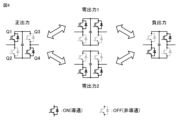
- FIG. 1A to 1C are diagrams illustrating the state of a cell 10 according to the first embodiment.
- 10 is a diagram illustrating combinations of conductive states of semiconductor switch elements Q1 to Q4 according to the first embodiment.
- FIG. 10A and 10B are diagrams illustrating timing for switching the state of cell 10 according to the first embodiment.
- 1A and 1B are diagrams illustrating the states of cells 10A and 10B according to a comparative example.
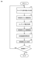
- FIG. 11 is a flow diagram illustrating a cell selection process of control circuit 50 according to the first embodiment.
- 13 is a diagram illustrating a function of a control circuit 51 according to the second embodiment.
- FIG. 11 is a diagram illustrating a cell switching procedure.
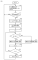
- FIG. 11 is a flow diagram illustrating a cell selection process of a control circuit according to a second embodiment.
- FIG. 11 is a flow diagram illustrating cell classification according to the second embodiment.
- FIG. 13 is a flow diagram illustrating cell classification according to the third embodiment.
- 13A to 13C are diagrams illustrating the capacitor voltages of the cells according to the comparative example and the third embodiment.
- FIG. 1 is a diagram illustrating a configuration of a power conversion device 1 according to a first embodiment.
- an example of a power conversion device 1 is provided with arm units 2A to 2C (hereinafter also collectively referred to as arm unit 2) for each of the three phases of a power transmission line 3, and a control circuit 50 that controls the arm units 2A to 2C.
- arm unit 2 for each phase is the same, so detailed description thereof will not be repeated.
- the configuration of arm unit 2A will be described as an example.
- the control circuit 50 will be described as controlling arm unit 2A as an example.
- the arm section 2A includes a plurality of cells 10A to 10C (collectively referred to as cells 10) and an interconnection reactor 11.
- FIG. 2 is a diagram illustrating a configuration of cell 10 according to the first embodiment.
- cell 10 includes a plurality of semiconductor switch elements Q1 to Q4, diodes Q1A to Q4A connected in parallel in the opposite directions to correspond to the plurality of semiconductor switch elements Q1 to Q4, a capacitor 101 which is a storage element, and a voltage detector 104 which detects the voltage of capacitor 101.
- Semiconductor switch element Q1 and semiconductor switch element Q2 are connected in series between node N1 and node N2.
- Semiconductor switch element Q3 and semiconductor switch element Q4 are connected in series between node N1 and node N2.
- Semiconductor switch elements Q1 and Q2, semiconductor switch elements Q3 and Q4, and capacitor 101 are connected in parallel between node N1 and node N2.
- voltage detector 104 that detects the voltage of capacitor 101 is connected between node N1 and node N2.
- Node Np which is the connection node between semiconductor switch element Q1 and semiconductor switch element Q2, is connected to node Nn of another cell 10 on the upstream side that is connected in series.
- Node Nn which is the connection node between semiconductor switch element Q3 and semiconductor switch element Q4, is connected to node Np of another downstream cell 10 connected in series.
- the node Np of the most upstream cell 10 is connected to an interconnection reactor 11 .
- This configuration is sometimes called an MMC (Modular Multilevel Converter), and in addition to control for exchanging power with the power grid, it requires balance control for equalizing the voltages of the capacitors of each cell.
- MMC Modular Multilevel Converter
- FIG. 3 is a diagram illustrating the function of control circuit 50 according to the first embodiment.
- the control circuit 50 includes a switching control unit 200 that controls the ON/OFF of the semiconductor switch elements Q1 to Q4 of the cells 10A to 10C, a capacitor voltage acquisition unit 201 that acquires the capacitor voltages of the cells 10A to 10C, and a state duration counting unit 202 that counts the duration of each state of the cells 10A to 10C.
- the capacitor voltage acquisition unit 201 acquires the voltage value of the capacitor 101 from the voltage detector 104 provided in each cell 10.
- the switching control unit 200 controls the ON/OFF of the semiconductor switch elements Q1 to Q4 of cells 10A to 10C at a predetermined timing, as described below.
- the switching control unit 200 executes PWM control to control the ON/OFF of the semiconductor switch elements Q1 to Q4 of the cells 10A to 10C based on the capacitor voltage of each cell 10A to 10C acquired by the capacitor voltage acquisition unit 201, the duration of the state of each cell 10A to 10C as measured by the state duration count unit 202, and the magnitude relationship between the command value and the carrier.
- cell 10 when semiconductor switch elements Q1 and Q4 are ON (conducting) and semiconductor switch elements Q2 and Q3 are OFF (non-conducting), cell 10 is in a positive output state in which the positive voltage of capacitor 101 is applied to the cell output terminal.
- the cell 10 is in a zero output state (part 1) in which it outputs zero voltage.
- the cell 10 is in a negative output state in which a negative voltage is applied.
- FIG. 6 is a diagram explaining the timing for switching the state of the cell 10 according to the first embodiment.
- the switching control unit 200 executes PWM control based on the magnitude relationship between the command value and the carrier. Specifically, the timing for switching the state of the cell 10 is determined by the magnitude relationship between the command value and the multiple triangular wave carriers, as shown on the horizontal axis for time and on the vertical axis for voltage or dimensionless quantity. That is, when the command value calculated based on the output current or capacitor voltage is positive, the switching control unit 200 judges to switch the cells 10 to the positive output state by the number of cells that exceed the carrier value.
- waveforms of carriers CA to CD in this example are merely examples and other waveforms may be used.
- carriers CC and CD may have waveforms that are linearly symmetrical to carriers CA and CB with the 0 line at the center.
- This method is sometimes called the sorting method. For example, if a current flows to discharge from the capacitor 101 when the cell 10 is switched from a zero output state to a positive output state, the switching control unit 200 can switch the multiple cells 10 to positive output in order starting with the cell 10 with the highest capacitor voltage, thereby achieving a good balance of the capacitor voltages of each cell 10.
- the switching control unit 200 can switch the multiple cells 10 to positive output in order starting with the cell 10 with the lowest capacitor voltage, thereby achieving a good balance of the capacitor voltages of each cell 10.
- the switching control unit 200 switches the cells 10 to the zero output state in order starting with the cell with the lowest capacitor voltage, thereby achieving a good balance of the capacitor voltages of each cell 10.
- the switching control unit 200 switches the cells 10 to the zero output state in order starting with the cell 10 with the highest capacitor voltage, thereby achieving a good balance of the capacitor voltages of each cell 10.
- FIG. 7 is a diagram illustrating the states of cells 10A and 10B according to a comparative example. Referring to FIG. 7A, the relationship between the triangular wave carrier and the command value is shown.
- cell 10A is switched to the zero output state for only a very short time.
- FIG. 7(B) is a diagram explaining the ON/OFF states of the semiconductor switch elements Q1 to Q4 according to a comparative example.
- the ON and OFF states of the semiconductor switch elements Q1 to Q4 of the first-stage cell 10A are shown when the state of cell 10A changes, but the semiconductor switch elements Q2 and Q3 are only in the ON state for a very short time.
- the semiconductor switch elements Q2 and Q3 may not be in the ON state for a sufficient amount of time, which may result in the destruction of the semiconductor switch elements Q2 and Q3.
- the minimum amount of time that the semiconductor switch elements must be in the ON state is sometimes called the minimum ON time.
- the minimum ON time is determined, for example, based on the withstand voltage or the upper limit of the switching frequency of the semiconductor switch elements.
- the predetermined time is a time given based on the characteristics of the semiconductor switch element constituting the cell (e.g., the voltage rating, current rating, upper limit value of the switching frequency, etc.), and is, for example, about several microseconds to several tens of microseconds.
- the predetermined time is a time longer than the minimum on-time described above, and may be set to any value by the designer. After a predetermined time has elapsed since the first-stage cell 10A entered the zero output state, the first-stage cell 10A again becomes a candidate for selection.
- cell 10A may be switched to the zero output state for a very short time, but if sufficient time has not passed since the first-stage cell 10A was in the zero output state, the next best candidate, cell 10B in the second stage, is switched to the positive output state.
- the first-stage cell 10A After a certain amount of time has elapsed, the first-stage cell 10A again becomes the candidate for selection, and in FIG. 8, the first-stage cell 10A is again switched to the positive output state.
- FIG. 8(B) is a diagram explaining the ON/OFF states of the semiconductor switch elements Q1 to Q4 according to the first embodiment.
- FIG. 9 is a flow diagram illustrating the cell selection process of the control circuit 50 according to the first embodiment.
- the switching control unit 200 executes a comparison process between the carrier and the command value (step S1).
- the switching control unit 200 calculates the number of cells whose state will change according to the comparison process (step S2).
- step S3 the voltage of the capacitor 101 of each cell 10 is acquired.
- the capacitor voltage acquisition unit 201 acquires the voltage of the capacitor 101 of each cell 10 and outputs it to the switching control unit 200.
- the switching control unit 200 extracts candidates for cells that change state according to the acquired voltage of the capacitor 101 (step S4). Specifically, the cell 10 with the high capacitor voltage is extracted as a candidate.
- step S5 the duration of the state is obtained (step S5). Specifically, the state duration counting unit 202 counts the time that the state of each cell 10 continues and outputs the count to the switching control unit 200.
- the switching control unit 200 determines the cell whose state is to be changed (step S6). Specifically, as described above, if a predetermined time has passed since the state was switched, the cell 10 with the highest priority is determined from among the extracted cell candidates. On the other hand, if a predetermined time has not passed since the state was switched, the cell with the next highest priority is determined as the cell whose state is to be changed. For the determined cell, the ON/OFF states of the semiconductor switch elements Q1 to Q4 are controlled according to the states described in Figures 4 and 5.
- step S7 it is determined whether the processing is completed (step S7).
- step S7 if it is determined that the processing has ended (YES in step S7), the processing ends (END).
- step S7 determines whether the process has ended (NO in step S7). If it is determined in step S7 that the process has not ended (NO in step S7), the process returns to step S1 and the above process is repeated. This process is executed at a predetermined interval.
- the number of cells and their states are not limited.
- the circuit diagram in Figure 1 shows a star-type wiring diagram, a delta-type wiring may also be used, or a double star-type wiring in which two star-type connections are connected may also be used.
- it may be configured with a single cell rather than multiple cells, and switching of the state of all cells may be prohibited until the duration of the cell state has elapsed for a specified time.
- a transformer may be installed in place of the interconnection reactor 11.
- cell 10 in FIG. 2 is described as being configured in a full-bridge configuration, a half-bridge configuration with a reduced number of semiconductor switch elements may also be used, and the semiconductor switch elements may be configured using not only IGBTs but also GCTs, MOSFETs, and other conceivable elements.
- a storage battery may be installed in place of the capacitor 101 .
- the carrier is level shifted, but the method is not limited to this. All of the figures are merely examples, and the configurations, components, and methods are not limited thereto.
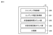
- FIG. 10 is a diagram illustrating the function of a control circuit 51 according to the second embodiment.
- control circuit 51 compared to the control circuit 50, the control circuit 51 further includes a state switching count unit 203 and a classification unit 204.
- the state switching count unit 203 counts the number of times the state has been switched for each cell 10.
- the classification unit 204 classifies the cells into groups for which state switching is to be performed preferentially based on the number of state switching times counted by the state switching count unit 203.
- the loss in the cell will be large, and the cell may generate heat and become too hot, shortening its lifespan.
- the capacitance of the capacitor 101 of the first-stage cell 10 is small, even if the same current flows through the capacitor 101, the capacitor voltage of the first-stage cell changes more than the capacitor voltage of the other cells 10. Therefore, the number of times the first-stage cell 10 is selected to equalize the capacitor voltages increases.
- the cells whose states are to be switched are selected mainly in ascending or descending order of the capacitor voltages of the cells, but in the method according to the second embodiment, an increase in the number of switching times of some of the cells 10 is suppressed.
- the cells 10 whose states are to be switched are selected taking into consideration not only the magnitude of the capacitor voltage but also the number of times each cell 10 switches its state. In other words, the number of times each cell switches its state is counted at each predetermined cycle, and cells that switch states a predetermined number of times or more are subordinated in the selection of the cells.
- FIG. 11 is a diagram illustrating a cell switching procedure. For example, a case will be described in which a current flows so as to discharge from a capacitor when switching from a zero output state to a positive output state.
- the cell 10A with the highest capacitor voltage is selected and switched to the positive output state.
- the number of switching times of the cell 10A is not taken into consideration, and the cell 10 to be switched to the positive output state is determined simply by the magnitude of the capacitor voltage, so there is a possibility that some cells 10 will switch more times than other cells 10.
- the switching order according to the second embodiment counts the number of cell switching times at a predetermined time interval, and prioritizes cells with a relatively large number of switching times.
- cells 10B and 10C have a larger number of switching times than cells 10A and 10D, and are therefore prioritized in the selection order.
- cells 10B and 10C are subordinated in selection, so they are called the subordinate group, while cells 10A and 10D are called the priority group.
- cells 10 are selected from the priority group in descending order of capacitor voltage and switched to the positive output state. After that, if a cell 10 is required to be switched to the positive output state, cells 10 are selected from the subordinate group in descending order of capacitor voltage. In this way, cells 10B and 10C, which have a relatively high number of switching times, are not given priority regardless of the magnitude of their capacitor voltages, and the number of switching times can be reduced.
- step S4 has been replaced with step S4A.
- the switching control unit 200 extracts candidates for cells that will change state from the priority group according to the acquired voltage of the capacitor 101 (step S4A). Specifically, cells 10 with high capacitor voltages are extracted as candidates from the pre-classified priority group. Note that if a cell 10 cannot be extracted from the priority group, a cell 10 is extracted as a candidate from the subordinate group.
- FIG. 13 is a flow diagram illustrating cell classification according to the second embodiment.
- state switching count unit 203 counts the state switching numbers N1 to Nk of the first to k-th cells (step S10).
- the classification unit 204 determines whether a predetermined period of time has elapsed (step S11).
- step S11 the classification unit 204 determines that the predetermined period has not elapsed (NO in step S11), the process returns to step S10 and continues the above counting.
- the classification unit 204 determines in step S11 that the predetermined period has elapsed (YES in step S11), it calculates the average value Navr of the state switching counts N1 to Nk (step S12). Specifically, the classification unit 204 calculates the average value Navr of the state switching counts N1 to Nk counted by the state switching counting unit 203.
- the classification unit 204 calculates the threshold value Nth (step S13).
- the threshold value Nth is calculated by Nvar ⁇ ⁇ ( ⁇ >1).
- the classification unit 204 determines in step S15 that the number of state switches Ni is greater than the threshold value Nth, it sets the i-th cell to the subordinate group (step S16).
- the classification unit 204 proceeds to step S18. Next, the classification unit 204 determines whether or not the condition i>k is satisfied (step S19).
- step S19 the classification unit 204 determines that the condition i>k is met (YES in step S19), it proceeds to the next step S20.
- step S20 the classification unit 204 instructs the state switching count unit 203 to reset the count and return to step S10.
- step S19 the classification unit 204 determines that the condition i>k is not satisfied (NO in step S19), the process returns to step S15 and repeats the above process.
- the classification unit 204 sets cells with a state switching count exceeding the threshold to a subordinate group, and sets cells with a state switching count below the threshold to a prioritized group.
- the above cells are determined according to the priority group and the subordinate group. The above operations are repeated at predetermined intervals.
- the number of switching events can be reduced by lowering the selection order in the present disclosure.
- Embodiment 3 In the second embodiment, the selection order of cells is explained taking into consideration the number of switching times, but using this method may make it difficult to balance the capacitor voltages. In the third embodiment, a method of classifying cells into a prioritized group and a subordinate group so as to balance the capacitor voltages will be explained.
- FIG. 14 is a flow diagram illustrating cell classification according to the third embodiment.
- the classification unit 204 detects the capacitor voltages Vdc1 to Vdck of the cells and calculates the average value Vavr (step S30).
- the classification unit 204 determines whether the capacitor voltage Vdcj is between the first threshold value Vthu and the second threshold value Vthl (step S33).
- step S33 If the classification unit 204 determines in step S33 that the capacitor voltage Vdcj is between the first threshold value Vthu and the second threshold value Vthl (YES in step S33), the jth cell maintains the current group (step S34). That is, if it is a subordinate group, it maintains the subordinate group. If it is a priority group, it maintains the priority group.
- step S33 if the classification unit 204 determines that the capacitor voltage Vdcj is not between the first threshold value Vthu and the second threshold value Vthl (NO in step S33), the j-th cell is set to the priority group (step S36). Then, the process proceeds to step S35.
- step S37 determines whether or not the condition j>k is satisfied (step S37). In step S37, if the classification unit 204 determines that the condition j>k is satisfied (YES in step S37), the processing ends (END).
- step S37 determines that the condition j>k is not satisfied (NO in step S37), the process returns to step S33 and repeats the above process.
- This process allows the classification unit 204 to reclassify cells that were once classified according to their capacitor voltages.
- the classification unit 204 executes the process at predetermined time intervals. Specifically, the process is repeatedly executed at an earlier timing than the initial classification.
- the capacitor voltage is within the range of Vthl to Vthu, the group to which it belongs is maintained as it is. In other words, the cells in the priority group are classified into the priority group, and the cells in the subordinate group are classified into the subordinate group. The above operations are repeated at regular intervals.
- FIG. 15 is a diagram explaining the capacitor voltage of a cell according to the comparative example and embodiment 3.
- the capacitor voltage of a cell according to the comparative example is shown to vary.
- 1 Power conversion device 2, 2A to 2C Arm section, 3 Power transmission line, 10, 10A, 10B, 10C, 10D Cell, 11 Interconnection reactor, 50, 51 Control circuit, 101 Capacitor, 104 Voltage detector, 200 Switching control section, 201 Capacitor voltage acquisition section, 202 State duration count section, 203 State switching count section, 204 Classification section.
Landscapes
- Engineering & Computer Science (AREA)
- Power Engineering (AREA)
- Physics & Mathematics (AREA)
- Electromagnetism (AREA)
- General Physics & Mathematics (AREA)
- Radar, Positioning & Navigation (AREA)
- Automation & Control Theory (AREA)
- Inverter Devices (AREA)
Abstract
Description
図1は、実施の形態1に従う電力変換装置1の構成について説明する図である。
図2は、実施の形態1に従うセル10の構成について説明する図である。
当該構成は、MMC(Modular Multilevel Converter)と呼ばれることもあり、電力系統と電力をやり取りするための制御のほかに、各セルのコンデンサの電圧を均等化するバランス制御が必要である。
図3を参照して、制御回路50は、セル10A~10Cの半導体スイッチ素子Q1~Q4のON/OFFを制御するスイッチング制御部200と、セル10A~10Cのコンデンサ電圧を取得するコンデンサ電圧取得部201と、セル10A~10Cのそれぞれの状態の継続時間をカウントする状態継続時間カウント部202とを含む。
図5は、実施の形態1に従う半導体スイッチ素子Q1~Q4の導通状態の組み合わせについて説明する図である。
具体的には、図6(A)を参照して、スイッチング制御部200は、指令値とキャリアとの大小関係に基づいてPWM制御を実行する。具体的には、セル10の状態を切り替えるタイミングは、横軸は時間、縦軸は電圧または無次元量に示すように、複数の三角波キャリアと指令値との大小関係によって定める。すなわち、スイッチング制御部200は、出力する電流やコンデンサ電圧によって算出された指令値が正の場合は、キャリアの値を上回った個数分だけ、セル10を正出力状態に切り替える判断を行う。また、スイッチング制御部200は、指令値が負の場合は、キャリアの値を下回った個数分だけ、セル10を負出力状態に切り替える判断を行う。その後、コンデンサ電圧、指令値の正負、電流の向きに応じて、どのセル10を出力状態にするか、あるいは零出力状態にするかの判断を行う。本例においては、キャリアCA~CDのうちキャリアCA,CBは正側に設けられており、キャリアCC,CDは負側に設けられている。キャリアCA,CBは常に0以上、キャリアCC,CDは常に0以下の領域となる。
例えば、スイッチング制御部200は、セル10を零出力状態から正出力状態に切り替えたときにコンデンサ101から放電するように電流が流れている場合は、複数のセル10のうちコンデンサ電圧が高いセル10から順に正出力に切り替えると、各セル10のコンデンサ電圧のバランスがよく取れる。
図1のある相で複数のセル10A~10Cが直列に接続されており、キャリアと指令値との大小関係から、「すべてのセルが零出力状態」と「1つのセルのみが正出力状態」との間を行き来する場合について考える。
図7(A)を参照して、三角波キャリアと指令値との関係が示される。
図8(A)を参照して、三角波キャリアと指令値との関係が示される。
ステップS7において、処理が終了したと判断した場合(ステップS7においてYES)には、処理を終了する(エンド)。
また、図6のレベルシフトPWM制御に関して、キャリアをレベルシフトさせているが、方式はこれに限定されない。いずれの図も例示であり、その構成、構成要素、方式を限定するものではない。
図10は、実施の形態2に従う制御回路51の機能について説明する図である。
状態が切り替わるセルは主にセルのコンデンサ電圧の降順または昇順により選択されるが、実施の形態2に従う方式では一部のセル10のスイッチング回数の増加を抑制する。
例えば、零出力状態から正出力状態に切り替えたときにコンデンサから放電するように電流が流れている場合について説明する。
図12は、実施の形態2に従う制御回路50のセルの選択の処理について説明するフロー図である。
図13を参照して、状態切替回数カウント部203は、1~k番目のセルの状態切替回数N1~Nkをカウントする(ステップS10)。
次に、分類部204は、所定期間が経過するか否かを判断する(ステップS11)。
次に、分類部204は、状態切替回数Niがしきい値Nthよりも大きいか否かを判断する(ステップS15)。
一方、ステップS15において、分類部204は、状態切替回数Niがしきい値Nthよりも小さいと判断した場合には、i番目のセルを優先群に設定する(ステップS16)。
次に、分類部204は、i>kの条件を満たすか否かを判断する(ステップS19)。
以上の操作を所定期間ごとに繰り返す。
実施の形態2において、切替回数を考慮したセルの選択順について説明したが、この方法を用いることでコンデンサ電圧のバランスが取りにくくなる場合がある。実施の形態3では、さらにコンデンサ電圧のバランスが取れるような優先群と劣後群の分類の仕方を説明する。
図14を参照して、分類部204は、セルのコンデンサ電圧Vdc1~Vdckを検出し、平均値Vavrを算出する(ステップS30)。
次に、分類部204は、初期値j=1に設定する。
一方、ステップS33において、分類部204は、コンデンサ電圧Vdcjが第1のしきい値Vthuと、第2のしきい値Vthlとの間に入っていないと判断した場合(ステップS33においてNO)には、j番目のセルを優先群に設定する(ステップS36)。そして、ステップS35に進む。
ステップS37において、分類部204は、j>kの条件を満たすと判断した場合(ステップS37においてYES)には、処理を終了する(エンド)。
Claims (6)
- アーム部と、
前記アーム部を制御する制御装置とを備え、
前記アーム部は、直列に接続された複数のセルを含み、
前記複数のセルは、
一対の接続端子と、
複数の半導体スイッチ素子と、
前記複数の半導体スイッチ素子に対して並列に接続された蓄電素子と、
前記蓄電素子の電圧を検出する電圧検出器とを含み、
前記制御装置は、
前記複数のセルのそれぞれに対応して、対応するセルの接続端子が正および負の少なくとも一方の電圧を出力する状態と、当該接続端子間を導通する状態とを少なくとも含む、いずれかの状態になるよう対応するセルに含まれる前記複数の半導体スイッチ素子の状態を切り替え可能であり、
所定のタイミングごとに、前記複数のセルがそれぞれ有する蓄電素子の電圧と、前記複数のセルの状態の継続時間とに基づいて状態を切り替える前記複数のセルのいずれか1つを選択し、
選択されたセルに含まれる前記複数の半導体スイッチ素子の状態を切り替える、電力変換装置。 - 前記制御装置は、前記選択されたセルの状態が切り替わってから所定の時間が経過するまで、当該セルが他の状態へ切り替えることを禁止する、請求項1に記載の電力変換装置。
- 前記制御装置は、前記所定のタイミングごとに、前記複数のセルがそれぞれ有する蓄電素子の電圧と、前記複数のセルの状態の継続時間と、前記複数のセルの状態の切り替え回数とに基づいて状態を切り替える前記複数のセルのいずれか1つを選択する、請求項1あるいは2に記載の電力変換装置。
- 前記制御装置は、
所定の周期ごとに状態を切り替えた回数を各セルごとにカウントし、
前記複数のセルのうち状態を切り替えた回数が所定の値以下であるセルを第1セル群、前記複数のセルのうち状態を切り替えた回数が所定の値を越えたセルを第2セル群に分類し、
前記所定のタイミングごとに状態を切り替えるセルを前記第1セル群の中から優先的に選択する、請求項3に記載の電力変換装置。 - 前記制御装置は、前記複数のセルのうち状態を切り替えた回数が所定の値を越え、かつ蓄電素子の電圧が所定の範囲内であるセルを第2セル群に分類する、請求項4に記載の電力変換装置。
- アーム部を含む電力変換装置の制御方法であって、
前記アーム部は、直列に接続された複数のセルを含み、前記複数のセルは、
一対の接続端子と、複数の半導体スイッチ素子と、前記複数の半導体スイッチ素子に対して並列に接続された蓄電素子と、前記蓄電素子の電圧を検出する電圧検出器とを含み、
所定のタイミングごとに、前記複数のセルがそれぞれ有する蓄電素子の電圧と、前記複数のセルの状態の継続時間とに基づいて状態を切り替える前記複数のセルのいずれか1つを選択するステップと、
選択されたセルに含まれる前記複数の半導体スイッチ素子の状態を、当該セルの接続端子が正および負の少なくとも一方の電圧を出力する状態と、当該接続端子間を導通する状態とを少なくとも含む、いずれかの状態になるよう切り替えるステップとを備える、電力変換装置の制御方法。
Priority Applications (3)
| Application Number | Priority Date | Filing Date | Title |
|---|---|---|---|
| JP2025525873A JPWO2024252628A1 (ja) | 2023-06-08 | 2023-06-08 | |
| PCT/JP2023/021394 WO2024252628A1 (ja) | 2023-06-08 | 2023-06-08 | 電力変換装置および電力変換装置の制御方法 |
| CN202380099194.2A CN121263754A (zh) | 2023-06-08 | 2023-06-08 | 电力转换装置以及电力转换装置的控制方法 |
Applications Claiming Priority (1)
| Application Number | Priority Date | Filing Date | Title |
|---|---|---|---|
| PCT/JP2023/021394 WO2024252628A1 (ja) | 2023-06-08 | 2023-06-08 | 電力変換装置および電力変換装置の制御方法 |
Publications (1)
| Publication Number | Publication Date |
|---|---|
| WO2024252628A1 true WO2024252628A1 (ja) | 2024-12-12 |
Family
ID=93795686
Family Applications (1)
| Application Number | Title | Priority Date | Filing Date |
|---|---|---|---|
| PCT/JP2023/021394 Ceased WO2024252628A1 (ja) | 2023-06-08 | 2023-06-08 | 電力変換装置および電力変換装置の制御方法 |
Country Status (3)
| Country | Link |
|---|---|
| JP (1) | JPWO2024252628A1 (ja) |
| CN (1) | CN121263754A (ja) |
| WO (1) | WO2024252628A1 (ja) |
Citations (4)
| Publication number | Priority date | Publication date | Assignee | Title |
|---|---|---|---|---|
| WO2016207976A1 (ja) * | 2015-06-23 | 2016-12-29 | 三菱電機株式会社 | 電力変換装置および直流送電システム |
| JP7275414B1 (ja) * | 2022-09-14 | 2023-05-17 | 三菱電機株式会社 | 電力変換装置および洋上風力発電システム |
| JP2023077915A (ja) * | 2021-11-25 | 2023-06-06 | 株式会社東芝 | 電力変換装置、電力変換装置の制御方法、およびプログラム |
| JP2023077976A (ja) * | 2021-11-25 | 2023-06-06 | 株式会社東芝 | 電力変換装置、電力変換装置の制御方法、およびプログラム |
-
2023
- 2023-06-08 WO PCT/JP2023/021394 patent/WO2024252628A1/ja not_active Ceased
- 2023-06-08 JP JP2025525873A patent/JPWO2024252628A1/ja active Pending
- 2023-06-08 CN CN202380099194.2A patent/CN121263754A/zh active Pending
Patent Citations (4)
| Publication number | Priority date | Publication date | Assignee | Title |
|---|---|---|---|---|
| WO2016207976A1 (ja) * | 2015-06-23 | 2016-12-29 | 三菱電機株式会社 | 電力変換装置および直流送電システム |
| JP2023077915A (ja) * | 2021-11-25 | 2023-06-06 | 株式会社東芝 | 電力変換装置、電力変換装置の制御方法、およびプログラム |
| JP2023077976A (ja) * | 2021-11-25 | 2023-06-06 | 株式会社東芝 | 電力変換装置、電力変換装置の制御方法、およびプログラム |
| JP7275414B1 (ja) * | 2022-09-14 | 2023-05-17 | 三菱電機株式会社 | 電力変換装置および洋上風力発電システム |
Also Published As
| Publication number | Publication date |
|---|---|
| JPWO2024252628A1 (ja) | 2024-12-12 |
| CN121263754A (zh) | 2026-01-02 |
Similar Documents
| Publication | Publication Date | Title |
|---|---|---|
| CN112994494B (zh) | 适用于飞跨电容多电平变换电路的电压平衡控制方法 | |
| Halamicek et al. | Cross-coupled series-capacitor quadruple step-down buck converter | |
| CN109039136B (zh) | 一种基于模块化多电平变流器的动力总成系统 | |
| Li et al. | Distributed balancing control for modular multilevel series/parallel converter with capability of sensorless operation | |
| CN106575928B (zh) | 模块化能量存储器直接转换器系统 | |
| Dam et al. | Low-frequency selection switch based cell-to-cell battery voltage equalizer with reduced switch count | |
| CN115065082B (zh) | 一种电池储能电站主回路构建方法、系统、设备和介质 | |
| TW201125259A (en) | Storage device with a balance circuit | |
| US10193446B2 (en) | Multi-module DC-to-DC power transformation system | |
| JP4643117B2 (ja) | マルチセル・エネルギー変換装置 | |
| CN113794373B (zh) | 多电平直流转换器及供电系统 | |
| Dahono et al. | A family of modular multilevel bidirectional DC-DC converters for high voltage-ratio and low-ripple applications | |
| US20180013290A1 (en) | Control circuit | |
| CN108736501A (zh) | 一种全桥型mmc的预充电方法 | |
| WO2024252628A1 (ja) | 電力変換装置および電力変換装置の制御方法 | |
| CN117996805A (zh) | 一种多级式储能变流器及其控制方法 | |
| JP5424337B2 (ja) | 時比率制御が可能な直列接続蓄電セル用均一充電器 | |
| CN112087134B (zh) | 一种储能型直接耦合式直流变压器及控制方法 | |
| CN108462482A (zh) | 一种产生双极性高压脉冲的装置和方法 | |
| WO2017027681A1 (en) | Column-switched multi-module dc-to-dc power transformation system | |
| CN114094833B (zh) | 开关电容接入式直流变压器及直流变压器的控制方法 | |
| Yue et al. | Investigation of control and applications of modular multilevel converter with sub-modular series igbts | |
| Kim et al. | Preventing voltage divergence in series-stacked bidirectional battery energy storage DC-DC converter under asymmetrical operating conditions | |
| JP6892996B2 (ja) | 直列接続された太陽電池又はその他の電源用の動作点制御のためのバランス回路装置 | |
| CN112187029A (zh) | 一种直流耗能装置 |
Legal Events
| Date | Code | Title | Description |
|---|---|---|---|
| 121 | Ep: the epo has been informed by wipo that ep was designated in this application |
Ref document number: 23940726 Country of ref document: EP Kind code of ref document: A1 |
|
| ENP | Entry into the national phase |
Ref document number: 2025525873 Country of ref document: JP Kind code of ref document: A |
|
| WWE | Wipo information: entry into national phase |
Ref document number: 202517119118 Country of ref document: IN |
|
| WWP | Wipo information: published in national office |
Ref document number: 202517119118 Country of ref document: IN |
|
| NENP | Non-entry into the national phase |
Ref country code: DE |