WO2024252697A1 - Substrat de mesure et procédé de fabrication de substrat de mesure - Google Patents
Substrat de mesure et procédé de fabrication de substrat de mesure Download PDFInfo
- Publication number
- WO2024252697A1 WO2024252697A1 PCT/JP2023/045689 JP2023045689W WO2024252697A1 WO 2024252697 A1 WO2024252697 A1 WO 2024252697A1 JP 2023045689 W JP2023045689 W JP 2023045689W WO 2024252697 A1 WO2024252697 A1 WO 2024252697A1
- Authority
- WO
- WIPO (PCT)
- Prior art keywords
- insulating member
- measurement substrate
- metal particles
- metal
- substrate according
- Prior art date
- Legal status (The legal status is an assumption and is not a legal conclusion. Google has not performed a legal analysis and makes no representation as to the accuracy of the status listed.)
- Ceased
Links
Images





Classifications
-
- B—PERFORMING OPERATIONS; TRANSPORTING
- B22—CASTING; POWDER METALLURGY
- B22F—WORKING METALLIC POWDER; MANUFACTURE OF ARTICLES FROM METALLIC POWDER; MAKING METALLIC POWDER; APPARATUS OR DEVICES SPECIALLY ADAPTED FOR METALLIC POWDER
- B22F1/00—Metallic powder; Treatment of metallic powder, e.g. to facilitate working or to improve properties
- B22F1/05—Metallic powder characterised by the size or surface area of the particles
- B22F1/054—Nanosized particles
-
- B—PERFORMING OPERATIONS; TRANSPORTING
- B22—CASTING; POWDER METALLURGY
- B22F—WORKING METALLIC POWDER; MANUFACTURE OF ARTICLES FROM METALLIC POWDER; MAKING METALLIC POWDER; APPARATUS OR DEVICES SPECIALLY ADAPTED FOR METALLIC POWDER
- B22F1/00—Metallic powder; Treatment of metallic powder, e.g. to facilitate working or to improve properties
- B22F1/18—Non-metallic particles coated with metal
-
- B—PERFORMING OPERATIONS; TRANSPORTING
- B22—CASTING; POWDER METALLURGY
- B22F—WORKING METALLIC POWDER; MANUFACTURE OF ARTICLES FROM METALLIC POWDER; MAKING METALLIC POWDER; APPARATUS OR DEVICES SPECIALLY ADAPTED FOR METALLIC POWDER
- B22F3/00—Manufacture of workpieces or articles from metallic powder characterised by the manner of compacting or sintering; Apparatus specially adapted therefor ; Presses and furnaces
- B22F3/24—After-treatment of workpieces or articles
-
- B—PERFORMING OPERATIONS; TRANSPORTING
- B22—CASTING; POWDER METALLURGY
- B22F—WORKING METALLIC POWDER; MANUFACTURE OF ARTICLES FROM METALLIC POWDER; MAKING METALLIC POWDER; APPARATUS OR DEVICES SPECIALLY ADAPTED FOR METALLIC POWDER
- B22F7/00—Manufacture of composite layers, workpieces, or articles, comprising metallic powder, by sintering the powder, with or without compacting wherein at least one part is obtained by sintering or compression
- B22F7/02—Manufacture of composite layers, workpieces, or articles, comprising metallic powder, by sintering the powder, with or without compacting wherein at least one part is obtained by sintering or compression of composite layers
- B22F7/04—Manufacture of composite layers, workpieces, or articles, comprising metallic powder, by sintering the powder, with or without compacting wherein at least one part is obtained by sintering or compression of composite layers with one or more layers not made from powder, e.g. made from solid metal
-
- G—PHYSICS
- G01—MEASURING; TESTING
- G01N—INVESTIGATING OR ANALYSING MATERIALS BY DETERMINING THEIR CHEMICAL OR PHYSICAL PROPERTIES
- G01N21/00—Investigating or analysing materials by the use of optical means, i.e. using sub-millimetre waves, infrared, visible or ultraviolet light
- G01N21/17—Systems in which incident light is modified in accordance with the properties of the material investigated
- G01N21/41—Refractivity; Phase-affecting properties, e.g. optical path length
Definitions
- the present invention relates to a measurement substrate and a method for manufacturing a measurement substrate.
- SPR surface plasmon resonance
- plasmons electron waves
- metal surfaces a mode of electron waves that couples with light occurs due to the boundary conditions specific to the surface. This is called surface plasmon.
- Methods for exciting surface plasmons include forming a diffraction grating on the metal surface to couple light with plasmons, and using evanescent waves.
- An example of a sensor that uses surface plasmon resonance is a sensor consisting of a total reflection prism and a metal film formed on the surface of the prism that comes into contact with a target substance.
- the refractive index of the surface changes depending on the minute amount of antigen adsorption in the antigen-antibody reaction, which changes the wavelength of the surface plasmon resonance, making it possible to sense the minute amount of antigen adsorption from the change in resonance wavelength.
- Patent Document 1 discloses a method for manufacturing a substrate for SPR measurement, which comprises an insulating member preparation step of preparing an insulating member having a positive or negative charge on its surface, a colloidal crystal dispersion preparation step of preparing a charged colloidal crystal dispersion in which colloidal crystals made of metal colloidal particles having an opposite charge to the surface charge of the insulating member are dispersed in a dispersion medium, and a surface formation step of contacting the insulating member with the charged colloidal crystal dispersion to form a single layer structure of metal colloidal crystals on the insulating member.
- a dispersion of charged colloidal crystals is brought into contact with an insulating member, and one layer of the charged colloidal crystals is adsorbed onto the insulating member by electrostatic attraction.
- a substrate for SPR measurement can be manufactured in which two-dimensional charged metal colloidal crystals are arranged at a predetermined lattice spacing on an insulating member.
- Patent Document 1 does not require complex pattern formation techniques such as lithography to control the arrangement of metal particles, making it easy to manufacture, and since two-dimensional charged metal colloidal crystals are arranged on an insulating member at a predetermined lattice spacing, it is possible to manufacture a substrate for SPR measurement that can be used to construct a localized surface plasmon sensor with high detection sensitivity.
- the particle diameter of the gold particles used as the metal particles is usually 150 to 200 nm. If the particle diameter is made larger than this, it becomes difficult to prepare a dispersion of colloidal crystals due to the effect of an increase in weight. As a result, it becomes difficult to form a two-dimensional colloidal crystallization layer on an insulating member.
- the present invention has been made to solve the above problems, and aims to provide a measurement substrate that can arrange metal particles in a single layer on an insulating member even if the particle diameter of the metal particles is large. Furthermore, the present invention aims to provide a manufacturing method for a measurement substrate that can form a single layer structure of metal colloid crystals made of metal particles on an insulating member even if the particle diameter of the metal particles is large.
- the measurement substrate of the present invention comprises an insulating member and metal particles arranged on the insulating member.
- the metal particles arranged on the insulating member are arranged in a single layer in at least a portion of the region.
- the metal particles have a core-shell structure including a core portion and a shell portion made of a metal that covers the core portion.
- the method for manufacturing a measurement substrate of the present invention includes an insulating member preparation step of preparing an insulating member having a positive or negative charge on its surface, a colloidal crystal dispersion preparation step of preparing a charged colloidal crystal dispersion in which metal colloidal crystals consisting of metal particles with a core-shell structure having an opposite charge to the surface charge of the insulating member are dispersed in a dispersion medium, and a surface formation step of contacting the charged colloidal crystal dispersion with the insulating member to form a monolayer structure of the metal colloidal crystals on the insulating member.
- the present invention it is possible to provide a measurement substrate that allows metal particles to be arranged in a single layer on an insulating member even if the particle diameter of the metal particles is large. Furthermore, according to the present invention, it is possible to provide a manufacturing method for a measurement substrate that allows a single layer structure of metal colloid crystals made of metal particles to be formed on an insulating member even if the particle diameter of the metal particles is large.
- FIG. 1 is a perspective view showing a schematic example of a measurement substrate of the present invention.
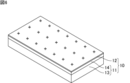
- FIG. 2 is a cross-sectional view that illustrates an example of the measurement substrate of the present invention.
- FIG. 3 is a plan view diagrammatically illustrating another example of the measuring substrate of the present invention.
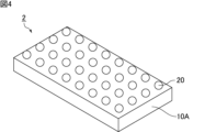
- FIG. 4 is a perspective view showing a schematic diagram of still another example of the measuring substrate of the present invention.
- FIG. 5 is a process diagram that illustrates an example of a method for producing a measurement substrate according to the present invention.
- FIG. 6 is a perspective view that illustrates an example of the insulating member prepared in the insulating member preparing step S11.
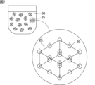
- FIG. 7 is a schematic diagram showing an example of the colloidal crystal dispersion liquid prepared in the colloidal crystal dispersion liquid preparation step S12.
- 8A and 8B are perspective views each showing a schematic example of the surface forming step S13.
- FIG. 9 is a perspective view that illustrates an example of a measuring substrate obtained by the measuring substrate
- the measurement substrate and the method for manufacturing the measurement substrate of the present invention will be described below.
- the present invention is not limited to the following embodiments, and can be appropriately modified and applied within the scope of the present invention.
- the present invention also includes a combination of two or more of the individual preferable configurations of the present invention described in the following embodiments.
- the measurement substrate of the present invention is used, for example, as an optical measurement substrate such as a surface plasmon resonance (SPR) measurement substrate.
- an optical measurement substrate such as a surface plasmon resonance (SPR) measurement substrate.
- SPR surface plasmon resonance
- FIG. 1 is a perspective view showing a schematic example of a measurement substrate of the present invention.
- FIG. 2 is a cross-sectional view showing a schematic example of a measurement substrate of the present invention.
- the measurement substrate 1 shown in Figures 1 and 2 includes an insulating member 10 and metal particles 20.
- the insulating member 10 is a conductive substrate 11 with an insulating film 12 provided on its surface.
- a MIM (Metal-Insulator-Metal) structure can be formed on the measurement substrate 1.
- the conductive substrate 11 is, for example, an insulating substrate 13 having a metal film 14 provided on its surface.
- the conductive substrate 11 may be a metal substrate, etc.
- Examples of insulating substrates 13 include glass substrates and ceramic substrates.
- the metal film 14 can be formed by methods such as vapor deposition, sputtering, and chemical plating.
- the type of metal film 14 is preferably a noble metal such as gold or silver that can exhibit strong plasmon resonance.
- the thickness of the metal film 14 is, for example, 1 nm or more and 100 nm or less. If the thickness of the metal film 14 is 100 nm or less, when the measurement substrate 1 is an SPR measurement substrate, the strength of the electric field due to the excitation of localized surface plasmons becomes stronger, and the sensitivity in the MIM-type SPR measurement becomes higher. In addition, if the thickness of the metal film 14 is 1 nm or more, pinholes are less likely to occur in the metal film 14.
- the insulating film 12 preferably has a positive or negative charge.
- the surface of the insulating member 10 preferably has a positive or negative charge.
- the insulating film 12 having a positive charge can be, for example, at least one type of insulating film selected from a silica film modified with a silane coupling agent having an aminopropyl group, and a film formed by adsorption of polyethyleneimine and poly(2-vinylpyridine).
- An example of the negatively charged insulating film 12 is a film formed by adsorption of a negatively charged polymer.
- a negatively charged polymer such as polyacrylic acid and polystyrene sulfonic acid, and introduction of negative charges such as silanol groups can be used.
- the thickness of the insulating film 12 is not particularly limited, and may be smaller than the thickness of the metal film 14, may be the same as the thickness of the metal film 14, or may be larger than the thickness of the metal film 14.
- the metal particles 20 are arranged in a single layer on the insulating member 10. In other words, the metal particles 20 are arranged two-dimensionally on the insulating member 10. It is preferable that the metal particles 20 are arranged in a single layer in all regions of the insulating member 10, but it is sufficient that the metal particles 20 are arranged in a single layer in at least some regions.
- the measurement substrate 1 is observed using a microscope such as an optical microscope or an electron microscope, if the metal particles 20 are observed only when the height of the sample stage is set to a certain height, it can be confirmed that the metal particles 20 are arranged in a single layer on the insulating member 10.
- the metal particle 20 has a core-shell structure including a core portion 21 and a shell portion 22 made of metal that covers the core portion 21.
- the specific gravity can be changed between the core portion 21 and the shell portion 22. Therefore, by making the specific gravity of the core portion 21 smaller than that of the shell portion 22, it is possible to suppress an increase in weight even if the particle diameter of the metal particles 20 is large, compared to when the metal particles 20 are solid particles made of metal. Therefore, it is possible to arrange metal particles 20 with large particle diameters in a single layer on the insulating member 10 using the method described below.
- the shell portion 22 only needs to cover at least a portion of the surface of the core portion 21. Therefore, the shell portion 22 may cover only a portion of the surface of the core portion 21, or may cover the entire surface of the core portion 21. There may be a mixture of metal particles 20 in which the shell portion 22 covers only a portion of the surface of the core portion 21, and metal particles 20 in which the shell portion 22 covers the entire surface of the core portion 21.
- the specific gravity of the core portion 21 is smaller than that of the shell portion 22.
- the particle diameter of the metal particles 20 can be increased, so that not only the near-infrared wavelength range (around 650 to 1000 nm), which is called the "biological window" and through which light easily passes through living organisms, but also higher wavelength ranges can be utilized, which is expected to improve the detection sensitivity as a biosensor.
- the peak wavelength of the surface plasmon resonance can be shifted to the longer wavelength side even if the particle diameter is the same, compared to when the metal particle 20 is a solid particle made of metal. This is presumably because the amplitude of the plasmon becomes larger due to the presence of an electrical insulator inside the metal particle 20.
- the core portion 21 is made of, for example, silicon oxide, titanium oxide, or polystyrene. From the viewpoint of making the particle diameter of the metal particles 20 uniform, silicon oxide such as SiO2 or titanium oxide such as TiO2 is preferable.
- the core portion 21 may be made of an inorganic material or an organic material.
- the core portion 21 may be made of an electrical insulator.
- the shell portion 22 is made of, for example, gold or silver. Gold is preferred from the viewpoint of suppressing oxidation and sulfurization of the metal particles 20.
- the core portion 21 is made of silicon oxide such as SiO2 and the shell portion 22 is made of gold.
- the shell portion 22 preferably has a charge of the opposite sign to the surface charge of the insulating member 10.
- the surface of the metal particle 20 preferably has a charge of the opposite sign to the surface charge of the insulating member 10.
- the metal particles 20 are arranged on the insulating member 10 at intervals due to the electrostatic repulsive force acting between the metal particles 20.
- the negatively charged metal particles 20 are adsorbed to the surface of the insulating member 10 by electrostatic attraction.
- a two-dimensional colloidal crystal in which metal particles 20 are regularly arranged is preferably formed on an insulating member 10.
- the metal particles 20 are regularly arranged two-dimensionally on the insulating member 10 with spaces between them.
- FIG. 3 is a plan view showing a schematic diagram of another example of a measurement substrate according to the present invention.
- a region (domain) in which metal particles 20 are regularly arranged in a two-dimensional manner may change orientation and become aggregated into a polycrystalline state.
- the distance between the metal particles 20 is not particularly limited, but if the distance between the metal particles 20 is too small, for example, it will be difficult for antibodies to enter, and the detection sensitivity will decrease. On the other hand, if the distance between the metal particles 20 is too large, there will be fewer metal particles 20 per unit area, and performance will decrease. For this reason, the distance between the metal particles 20 needs to be set appropriately. By setting the distance between the metal particles 20 appropriately, for example, when the measurement substrate 1 is an SPR measurement substrate, surface plasmon resonance can be actively generated.
- the distance between metal particles 20 is measured as the average interparticle distance for 100 to 200 metal particles 20 in a plan view such as that shown in Figure 3.
- the average particle size of the metal particles 20 is preferably 100 nm or more and 500 nm or less.
- the metal particles 20 have a core-shell structure, even if the average particle diameter of the metal particles 20 is 100 nm or more, the metal particles 20 can be arranged in a single layer on the insulating member 10.
- the average particle diameter of the metal particles 20 may be 150 nm or more, or 200 nm or more.
- the average particle size of the metal particles 20 is 500 nm or less, the settling speed in the liquid medium will be slow, making it easier to produce three-dimensional crystals in the manufacturing method described below.
- the average particle size of the metal particles 20 may be 450 nm or less, or may be 400 nm or less.
- the average particle size of the metal particles 20 is measured as the average particle size (diameter) of 100 or more and 200 or less metal particles 20 in a plan view such as that shown in Figure 3.
- FIG. 4 is a perspective view showing a schematic diagram of yet another example of a measurement substrate according to the present invention.
- the measurement substrate 2 shown in FIG. 4 includes an insulating member 10A and metal particles 20.
- the insulating member 10A is an insulating substrate.
- examples of the insulating member 10A include a glass substrate and a ceramic substrate.
- the measurement substrate 2 shown in FIG. 4 has a common configuration with the measurement substrate 1 shown in FIG. 1, except that it has an insulating member 10A instead of the insulating member 10. As with the insulating member 10, it is preferable that the surface of the insulating member 10A has a positive or negative charge.
- the measurement substrate of the present invention is preferably manufactured by the following method.
- FIG. 5 is a process diagram that shows a schematic example of a method for manufacturing a measurement substrate according to the present invention.
- the manufacturing method of the measurement substrate of the present invention includes an insulating member preparation process S11, a colloidal crystal dispersion preparation process S12, and a surface formation process S13.
- FIG. 6 is a schematic perspective view of an example of an insulating member prepared in the insulating member preparation step S11.
- an insulating member 10 having a positive or negative charge on its surface is prepared.
- the surface of the insulating member 10 has a positive charge.
- an insulating member 10 is prepared, which is a conductive substrate 11 having an insulating film 12 provided on its surface.
- the conductive substrate 11 is, for example, an insulating substrate 13 having a metal film 14 provided on its surface.
- the conductive substrate 11 may be a metal substrate, etc.
- an insulating substrate an insulating member 10A
- the surface of the insulating member 10A has a positive or negative charge.
- FIG. 7 is a schematic diagram showing an example of a colloidal crystal dispersion liquid prepared in the colloidal crystal dispersion liquid preparation step S12.
- a charged colloidal crystal dispersion liquid 30 is prepared in which metal colloidal crystals 25 made of metal particles 20 with a core-shell structure having a charge of the opposite sign to the surface charge of the insulating member 10 are dispersed in a dispersion medium.
- the surfaces of the metal particles 20 have a negative charge.
- the metal particle 20 has a core-shell structure including a core portion 21 and a shell portion 22 made of a metal that covers the core portion 21.
- a compound e.g., sodium 3-mercapto-1-propanesulfonate (MPS)
- a functional group e.g., mercapto group, etc.
- a functional group that forms a negative charge e.g., sulfonic acid group or carboxylic acid group, etc.
- FIGS. 8A and 8B are perspective views that show a schematic example of the surface formation process S13.
- the insulating member 10 is contacted with a charged colloidal crystal dispersion liquid 30 to form a single layer structure of metal colloidal crystals 25 on the insulating member 10.
- a negatively (or positively) charged colloidal crystal dispersion 30 is brought into contact with an insulating member 10 having a positive (or negative) charge, and only one layer of the colloidal crystal lattice is adsorbed to the insulating member 10 by electrostatic attraction, and then the excess charged colloidal crystal dispersion 30 is washed away by washing with a solvent such as water.
- FIG. 9 is a schematic perspective view of an example of a measurement substrate obtained by the measurement substrate manufacturing method of the present invention.
- a measurement substrate 1 is obtained in which a two-dimensional colloidal crystal of metal particles 20 is formed on an insulating member 10.
- the method for manufacturing a measurement substrate of the present invention forms a single layer structure of metal colloidal crystals, making it possible to control the arrangement of metal particles without using complex pattern formation techniques. This makes it easy to manufacture the measurement substrate, and allows the construction of a sensor with high detection sensitivity.
- the metal particles have a core-shell structure including a core portion and a shell portion made of a metal that covers the core portion.
- ⁇ 3> The measurement substrate according to ⁇ 1> or ⁇ 2>, wherein the measurement substrate is an optical measurement substrate.
- ⁇ 4> The measurement substrate according to ⁇ 3>, wherein the measurement substrate is a substrate for surface plasmon resonance measurement.
- ⁇ 5> The measurement substrate according to any one of ⁇ 1> to ⁇ 4>, wherein the average particle diameter of the metal particles is 100 nm or more and 500 nm or less.
- ⁇ 6> The measurement substrate according to any one of ⁇ 1> to ⁇ 5>, wherein the specific gravity of the core portion is smaller than the specific gravity of the shell portion.
- ⁇ 7> The measurement substrate according to ⁇ 6>, wherein the core portion is made of silicon oxide, titanium oxide or polystyrene.
- ⁇ 9> The measuring substrate according to any one of ⁇ 1> to ⁇ 8>, wherein the insulating member is an insulating substrate.
- insulating member is a conductive substrate having an insulating film provided on a surface thereof.
- ⁇ 11> The measurement substrate according to any one of ⁇ 1> to ⁇ 10>, wherein a two-dimensional colloidal crystal in which the metal particles are regularly arranged is formed on the insulating member.
- ⁇ 14> The method for producing a measurement substrate according to ⁇ 13>, wherein the measurement substrate is a substrate for surface plasmon resonance measurement.
- ⁇ 15> The method for manufacturing a measurement substrate according to any one of ⁇ 12> to ⁇ 14>, wherein an average particle diameter of the metal particles is 100 nm or more and 500 nm or less.
- ⁇ 16> The method for manufacturing a measurement substrate according to any one of ⁇ 12> to ⁇ 15>, wherein the specific gravity of the core portion is smaller than the specific gravity of the shell portion.
- ⁇ 17> The method for producing a measurement substrate according to ⁇ 16>, wherein the core portion is made of silicon oxide, titanium oxide or polystyrene.
- ⁇ 18> The method for manufacturing a measurement substrate according to ⁇ 16> or ⁇ 17>, wherein the shell portion is made of gold or silver.
- ⁇ 19> The method for manufacturing a measurement substrate according to any one of ⁇ 12> to ⁇ 18>, wherein the insulating member is an insulating substrate.
- ⁇ 20> The method for manufacturing a measurement substrate according to any one of ⁇ 12> to ⁇ 18>, wherein the insulating member is a conductive substrate having an insulating film provided on a surface thereof.
Landscapes
- Engineering & Computer Science (AREA)
- Chemical & Material Sciences (AREA)
- Mechanical Engineering (AREA)
- Manufacturing & Machinery (AREA)
- Analytical Chemistry (AREA)
- Composite Materials (AREA)
- General Health & Medical Sciences (AREA)
- General Physics & Mathematics (AREA)
- Immunology (AREA)
- Pathology (AREA)
- Physics & Mathematics (AREA)
- Biochemistry (AREA)
- Life Sciences & Earth Sciences (AREA)
- Materials Engineering (AREA)
- Health & Medical Sciences (AREA)
- Inorganic Chemistry (AREA)
- Nanotechnology (AREA)
- Investigating Or Analysing Materials By Optical Means (AREA)
Abstract
Substrat de mesure (1) comprenant un élément isolant (10) ; et des particules métalliques (20) disposées sur l'élément isolant (10). Les particules métalliques (20) disposées sur l'élément isolant (10) sont agencées en une seule couche dans au moins une partie de la région. Les particules métalliques (20) ont chacune une structure noyau-enveloppe qui comprend une partie noyau (21) et une partie coque (22) recouvrant la partie noyau (21) et composée d'un métal.
Priority Applications (1)
| Application Number | Priority Date | Filing Date | Title |
|---|---|---|---|
| JP2025525933A JPWO2024252697A1 (fr) | 2023-06-09 | 2023-12-20 |
Applications Claiming Priority (2)
| Application Number | Priority Date | Filing Date | Title |
|---|---|---|---|
| JP2023095591 | 2023-06-09 | ||
| JP2023-095591 | 2023-06-09 |
Publications (1)
| Publication Number | Publication Date |
|---|---|
| WO2024252697A1 true WO2024252697A1 (fr) | 2024-12-12 |
Family
ID=93795864
Family Applications (1)
| Application Number | Title | Priority Date | Filing Date |
|---|---|---|---|
| PCT/JP2023/045689 Ceased WO2024252697A1 (fr) | 2023-06-09 | 2023-12-20 | Substrat de mesure et procédé de fabrication de substrat de mesure |
Country Status (2)
| Country | Link |
|---|---|
| JP (1) | JPWO2024252697A1 (fr) |
| WO (1) | WO2024252697A1 (fr) |
Citations (3)
| Publication number | Priority date | Publication date | Assignee | Title |
|---|---|---|---|---|
| JP2010127928A (ja) * | 2008-11-29 | 2010-06-10 | Korea Electronics Telecommun | バイオ物質感知用ナノ粒子及びこれを利用したバイオセンサ |
| JP2013522639A (ja) * | 2010-03-22 | 2013-06-13 | アイメック | 表面増強光検出のための方法およびシステム |
| JP2020034543A (ja) * | 2018-08-28 | 2020-03-05 | 公立大学法人名古屋市立大学 | Spr測定用基板及びその製造方法 |
-
2023
- 2023-12-20 WO PCT/JP2023/045689 patent/WO2024252697A1/fr not_active Ceased
- 2023-12-20 JP JP2025525933A patent/JPWO2024252697A1/ja active Pending
Patent Citations (3)
| Publication number | Priority date | Publication date | Assignee | Title |
|---|---|---|---|---|
| JP2010127928A (ja) * | 2008-11-29 | 2010-06-10 | Korea Electronics Telecommun | バイオ物質感知用ナノ粒子及びこれを利用したバイオセンサ |
| JP2013522639A (ja) * | 2010-03-22 | 2013-06-13 | アイメック | 表面増強光検出のための方法およびシステム |
| JP2020034543A (ja) * | 2018-08-28 | 2020-03-05 | 公立大学法人名古屋市立大学 | Spr測定用基板及びその製造方法 |
Non-Patent Citations (1)
| Title |
|---|
| NICOLAS RANA, LÉVÊQUE GAËTAN, MARAE-DJOUDA JOSEPH, MONTAY GUILLAME, MADI YAZID, PLAIN JÉRÔME, HERRO ZIAD, KAZAN MICHEL, ADAM PIERR: "Plasmonic mode interferences and Fano resonances in Metal-Insulator- Metal nanostructured interface", SCIENTIFIC REPORTS, NATURE PUBLISHING GROUP, US, vol. 5, no. 1, US , XP093246225, ISSN: 2045-2322, DOI: 10.1038/srep14419 * |
Also Published As
| Publication number | Publication date |
|---|---|
| JPWO2024252697A1 (fr) | 2024-12-12 |
Similar Documents
| Publication | Publication Date | Title |
|---|---|---|
| Wang et al. | Research advances on surface plasmon resonance biosensors | |
| Kaushik et al. | Two-dimensional transition metal dichalcogenides assisted biofunctionalized optical fiber SPR biosensor for efficient and rapid detection of bovine serum albumin | |
| Mariani et al. | Decoration of porous silicon with gold nanoparticles via layer-by-layer nanoassembly for interferometric and hybrid photonic/plasmonic (bio) sensing | |
| Qian et al. | Three-dimensionally ordered macroporous polymer materials: An approach for biosensor applications | |
| Jenkins et al. | Blue-shifted narrow localized surface plasmon resonance from dipole coupling in gold nanoparticle random arrays | |
| Chen et al. | Shape-dependent refractive index sensitivities of gold nanocrystals with the same plasmon resonance wavelength | |
| Martinsson et al. | Substrate effect on the refractive index sensitivity of silver nanoparticles | |
| Kang et al. | Durable plasmonic cap arrays on flexible substrate with real-time optical tunability for high-fidelity SERS devices | |
| US10520442B2 (en) | Nanogap structure having ultrasmall void between metal cores and molecular sensing apparatus and method using the same, and method for preparing the nanogap structure by selective etching | |
| Solanki et al. | A chitosan modified nickel oxide platform for biosensing applications | |
| He et al. | Suspension array with shape-coded silica nanotubes for multiplexed immunoassays | |
| JP7253169B2 (ja) | Spr測定用基板及びその製造方法 | |
| CN111213051B (zh) | 用于确定分析物的纳米传感器方法和装置 | |
| WO2012169971A1 (fr) | Procédé de génération d'une métamatière et métamatière générée | |
| Li et al. | Fabrication of an insect-like compound-eye SERS substrate with 3D Ag nano-bowls and its application in optical sensor | |
| Schalkhammer | Metal nano clusters as transducers for bioaffinity interactions | |
| Zhao et al. | TiN nanorods as effective substrate for surface-enhanced Raman scattering | |
| JP2005144569A (ja) | 二次元配列構造体基板および該基板から剥離した微粒子 | |
| Zhang et al. | Metallic nanoshells with sub-10 nm thickness and their performance as surface-enhanced spectroscopy substrate | |
| Matsubara et al. | Effects of adsorbed water on plasmon-based dissolution, redeposition and resulting spectral changes of Ag nanoparticles on single-crystalline TiO 2 | |
| US20240402165A1 (en) | Spiky metal structures | |
| KR20090061455A (ko) | 광학적 특성을 이용한 분석용 센서를 위한 기판 제조 방법및 그 기판 | |
| Putranto et al. | Block copolymer self-assembly for biological and chemical sensing | |
| Zhang et al. | Silver nanopillar arrayed thin films with highly surface-enhanced Raman scattering for ultrasensitive detection | |
| WO2024252697A1 (fr) | Substrat de mesure et procédé de fabrication de substrat de mesure |
Legal Events
| Date | Code | Title | Description |
|---|---|---|---|
| 121 | Ep: the epo has been informed by wipo that ep was designated in this application |
Ref document number: 23940791 Country of ref document: EP Kind code of ref document: A1 |
|
| ENP | Entry into the national phase |
Ref document number: 2025525933 Country of ref document: JP Kind code of ref document: A |
|
| WWE | Wipo information: entry into national phase |
Ref document number: 2025525933 Country of ref document: JP |
|
| NENP | Non-entry into the national phase |
Ref country code: DE |