WO2024252787A1 - Power conversion device - Google Patents
Power conversion device Download PDFInfo
- Publication number
- WO2024252787A1 WO2024252787A1 PCT/JP2024/014915 JP2024014915W WO2024252787A1 WO 2024252787 A1 WO2024252787 A1 WO 2024252787A1 JP 2024014915 W JP2024014915 W JP 2024014915W WO 2024252787 A1 WO2024252787 A1 WO 2024252787A1
- Authority
- WO
- WIPO (PCT)
- Prior art keywords
- switching
- power conversion
- switching element
- terminal
- resonant
- Prior art date
- Legal status (The legal status is an assumption and is not a legal conclusion. Google has not performed a legal analysis and makes no representation as to the accuracy of the status listed.)
- Ceased
Links
Images





Classifications
-
- H—ELECTRICITY
- H02—GENERATION; CONVERSION OR DISTRIBUTION OF ELECTRIC POWER
- H02M—APPARATUS FOR CONVERSION BETWEEN AC AND AC, BETWEEN AC AND DC, OR BETWEEN DC AND DC, AND FOR USE WITH MAINS OR SIMILAR POWER SUPPLY SYSTEMS; CONVERSION OF DC OR AC INPUT POWER INTO SURGE OUTPUT POWER; CONTROL OR REGULATION THEREOF
- H02M7/00—Conversion of AC power input into DC power output; Conversion of DC power input into AC power output
- H02M7/42—Conversion of DC power input into AC power output without possibility of reversal
- H02M7/44—Conversion of DC power input into AC power output without possibility of reversal by static converters
- H02M7/48—Conversion of DC power input into AC power output without possibility of reversal by static converters using discharge tubes with control electrode or semiconductor devices with control electrode
-
- Y—GENERAL TAGGING OF NEW TECHNOLOGICAL DEVELOPMENTS; GENERAL TAGGING OF CROSS-SECTIONAL TECHNOLOGIES SPANNING OVER SEVERAL SECTIONS OF THE IPC; TECHNICAL SUBJECTS COVERED BY FORMER USPC CROSS-REFERENCE ART COLLECTIONS [XRACs] AND DIGESTS
- Y02—TECHNOLOGIES OR APPLICATIONS FOR MITIGATION OR ADAPTATION AGAINST CLIMATE CHANGE
- Y02B—CLIMATE CHANGE MITIGATION TECHNOLOGIES RELATED TO BUILDINGS, e.g. HOUSING, HOUSE APPLIANCES OR RELATED END-USER APPLICATIONS
- Y02B70/00—Technologies for an efficient end-user side electric power management and consumption
- Y02B70/10—Technologies improving the efficiency by using switched-mode power supplies [SMPS], i.e. efficient power electronics conversion e.g. power factor correction or reduction of losses in power supplies or efficient standby modes
Definitions
- This disclosure relates to a power conversion device, and more specifically, to a power conversion device capable of converting DC power to AC power.
- Patent Document 1 discloses a resonant inverter device (power conversion device).
- the DC voltage of the DC voltage source is converted to AC voltage by an inverter section (power conversion circuit).
- This inverter section is configured with six main switching elements (three first switching elements and three second switching elements) bridge-connected in three phases (U phase, V phase, and W phase) between the positive bus and the negative bus.
- two voltage-dividing capacitors are connected in series between the positive bus and the negative bus. These two voltage-dividing capacitors constitute a voltage-dividing means for dividing the DC voltage of the DC voltage source, and also constitute a means for generating a voltage that is 1/2 the DC voltage of the DC voltage source at the connection point between them. Furthermore, a resonant circuit section is provided between the two voltage-dividing capacitors and the inverter section for performing a resonant operation when the main switching element is switched.
- This resonant circuit section is configured such that a series circuit consisting of a resonant reactor (resonant inductor) and an auxiliary switch (switch) is connected between the connection point of the two voltage-dividing capacitors and the connection point of the upper and lower arms of each phase, and a resonant capacitor is connected in parallel to each series circuit.
- the inverter section has three inverter arms (switching circuits). In each of the three inverter arms, the main switching element (first switching element) of the upper arm and the main switching element (second switching element) of the lower arm are connected in series.
- Each main switching element and each auxiliary switch is controlled on and off by the control unit.
- the first switching element and the second switching element connected to the failed auxiliary switch may each be hard-switched.
- the objective of this disclosure is to provide a power conversion device that can detect a switching circuit in which hard switching has occurred.
- a power conversion device includes a first DC terminal and a second DC terminal, a power conversion circuit, a plurality of AC terminals, a plurality of switches, a plurality of resonant capacitors, at least one resonant inductor, a regenerative capacitor, and a control device.
- the power conversion circuit has a plurality of first switching elements and a plurality of second switching elements.
- a plurality of switching circuits in which the plurality of first switching elements and the plurality of second switching elements are connected in series in a one-to-one relationship are connected in parallel to each other.
- the plurality of first switching elements are connected to the first DC terminal, and the plurality of second switching elements are connected to the second DC terminal.
- the plurality of AC terminals correspond one-to-one to the plurality of switching circuits.
- Each of the plurality of AC terminals is connected to a connection point of the first switching element and the second switching element in a corresponding one of the plurality of switching circuits.
- the plurality of switches correspond one-to-one to the plurality of switching circuits.
- Each of the plurality of switches has a first end and a second end, and the first end is connected to the connection point of the first switching element and the second switching element in a corresponding switching circuit among the plurality of switching circuits.
- the plurality of resonance capacitors correspond one-to-one to the plurality of switches.
- Each of the plurality of resonance capacitors is connected between the first end and the second DC terminal of a corresponding switch among the plurality of switches.
- the at least one resonance inductor has a third end and a fourth end. In the at least one resonance inductor, the third end is connected to the second end of the corresponding switch among the plurality of switches.
- the regeneration capacitor has a fifth end and a sixth end. In the regeneration capacitor, the fifth end is connected to the second DC terminal, and the sixth end is connected to the fourth end of the at least one resonance inductor.
- the control device controls the on/off of each of the plurality of first switching elements, the plurality of second switching elements, and the plurality of switches.
- the control device has a first determination unit and a second determination unit.
- the first determination unit determines the switching state of the power conversion circuit based on a ripple voltage included in the voltage across the regenerative capacitor and the multiple load currents output from the multiple AC terminals.
- the second determination unit determines which of the multiple switching circuits is experiencing hard switching based on the polarity of the multiple load currents in a specific phase of the ripple voltage.
- a power conversion device includes a first DC terminal and a second DC terminal, a power conversion circuit, a plurality of AC terminals, a plurality of switches, a plurality of resonant capacitors, at least one resonant inductor, a regenerative capacitor, and a control device.
- the power conversion circuit has a plurality of first switching elements and a plurality of second switching elements.
- a plurality of switching circuits in which the plurality of first switching elements and the plurality of second switching elements are connected in series in a one-to-one relationship are connected in parallel to each other.
- the plurality of first switching elements are connected to the first DC terminal, and the plurality of second switching elements are connected to the second DC terminal.
- the plurality of AC terminals correspond one-to-one to the plurality of switching circuits.
- Each of the plurality of AC terminals is connected to a connection point of the first switching element and the second switching element in a corresponding one of the plurality of switching circuits.
- the plurality of switches correspond one-to-one to the plurality of switching circuits.
- Each of the plurality of switches has a first end and a second end, and the first end is connected to the connection point of the first switching element and the second switching element in a corresponding switching circuit among the plurality of switching circuits.
- the plurality of resonance capacitors correspond one-to-one to the plurality of switches.
- Each of the plurality of resonance capacitors is connected between the first end and the second DC terminal of a corresponding switch among the plurality of switches.
- the at least one resonance inductor has a third end and a fourth end. In the at least one resonance inductor, the third end is connected to the second end of the corresponding switch among the plurality of switches.
- the regeneration capacitor has a fifth end and a sixth end. In the regeneration capacitor, the fifth end is connected to the second DC terminal, and the sixth end is connected to the fourth end of the at least one resonance inductor.
- the control device controls the on/off of each of the plurality of first switching elements, the plurality of second switching elements, and the plurality of switches.
- the control device has a first determination unit and a second determination unit.
- the first determination unit determines the switching state of the power conversion circuit based on a ripple voltage included in the voltage across the regenerative capacitor and the multiple load currents output from the multiple AC terminals.
- the second determination unit determines which of the multiple switching circuits is experiencing hard switching based on control signals provided to each of the multiple switches.
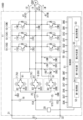
- FIG. 1 is a circuit diagram of a system including a power conversion device according to a first embodiment.
- Fig. 2A is a waveform diagram for explaining the relationship between the load current and the voltage across the regenerative capacitor when the power conversion device is operating normally.
- Fig. 2B is a waveform diagram for explaining the relationship between the load current and the voltage across the regenerative capacitor when the power conversion device is operating abnormally.
- Fig. 3A is a waveform diagram for explaining the relationship between the load current and the voltage across the regenerative capacitor when the U-phase switch in the power conversion device of the above-mentioned embodiment fails.
- Fig. 2A is a waveform diagram for explaining the relationship between the load current and the voltage across the regenerative capacitor when the power conversion device is operating normally.
- Fig. 3A is a waveform diagram for explaining the relationship between the load current and the voltage across the regenerative capacitor when the U-phase switch in the power conversion device of the above-mentioned embodiment fails.
- Fig. 1 is
- FIG. 3B is a waveform diagram for explaining the relationship between the load current and the voltage across the regenerative capacitor when the V-phase switch in the power conversion device of the above-mentioned embodiment fails.
- Fig. 3C is a waveform diagram for explaining the relationship between the load current and the voltage across the regenerative capacitor when the V-phase switch in the power conversion device of the above-mentioned embodiment fails.
- FIG. 4 is a diagram illustrating the operation of the power conversion device when hard switching occurs in the U-phase switching circuit.
- FIG. 5 is a waveform diagram for explaining the relationship between the load current and the voltage across the regenerative capacitor when the V-phase switch and the W-phase switch fail in the power conversion device.
- FIG. 6A is a waveform diagram for explaining the relationship between the load current and the voltage across the regenerative capacitor when the power conversion device is operating normally
- Fig. 6B is a waveform diagram for explaining the relationship between the load current and the voltage across the regenerative capacitor when the switches of the U-phase, V-phase, and W-phase in the power conversion device are faulty.
- FIG. 7 is an explanatory diagram of an operation when the control device in the power conversion device performs a basic operation when the load current is greater than 0 and the resonance capacitor is being charged.
- FIG. 8 is another operation explanatory diagram when the control device in the power conversion device performs a basic operation in the case where the load current is greater than 0 and the resonance capacitor is being charged.
- FIG. 7 is an explanatory diagram of an operation when the control device in the power conversion device performs a basic operation when the load current is greater than 0 and the resonance capacitor is being charged.
- FIG. 8 is another operation explanatory diagram when the control device in the power conversion device performs
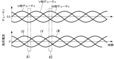
- FIG. 9 is a diagram showing a time change in duty and a time change in load current corresponding to voltage commands for each of three phases in an AC load connected to a plurality of AC terminals of the power conversion device according to the above embodiment.
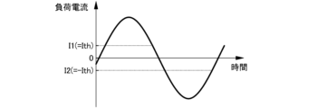
- FIG. 10 is an explanatory diagram of a first current threshold value and a second current threshold value used by a control device in the power conversion device according to the above embodiment.
- FIG. 11 is an explanatory diagram of an operation when the control device in the power conversion device performs a basic operation when the load current is greater than 0 and the resonant capacitor is discharging.
- FIG. 12 is an explanatory diagram of an operation when the control device in the power conversion device performs a basic operation when the load current is less than 0 and the resonant capacitor is discharging.
- FIG. 13 is an explanatory diagram of an operation when the control device in the power conversion device performs a basic operation when the load current is less than 0 and the resonance capacitor is being charged.
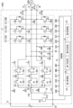
- FIG. 14 is a circuit diagram of a system including a power conversion device according to the second embodiment.
- FIG. 15 is a diagram illustrating the operation of the power conversion device.
- FIG. 16 is a diagram illustrating the operation of the power conversion device.
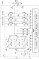
- FIG. 17 is a circuit diagram of a system including a power conversion device according to the third embodiment.
- FIG. 18 is a circuit diagram of a system including a power conversion device according to the fourth embodiment.
- FIG. 19 is a circuit diagram of a system including a power conversion device according to a first modification of the fourth embodiment.
- FIG. 20 is a circuit diagram of a system including a power conversion device according to a second modification of the fourth embodiment.
- FIG. 21 is a circuit diagram of a system including a power conversion device according to a third modification of the fourth embodiment.
- FIG. 22 is a circuit diagram of a system including a power conversion device according to a fourth modification of the fourth embodiment.
- FIG. 23 is a circuit diagram of a system including a power conversion device according to the fifth embodiment.
- the power conversion device 100 includes a first DC terminal 31, a second DC terminal 32, and a plurality of (e.g., three) AC terminals 41.
- a DC power source E1 is connected between the first DC terminal 31 and the second DC terminal 32, and an AC load RA1 is connected to the plurality of AC terminals 41.
- the AC load RA1 is, for example, a three-phase motor.
- the power conversion device 100 converts the DC output from the DC power source E1 into AC power and outputs it to the AC load RA1.
- the DC power source E1 includes, for example, a solar cell or a fuel cell.
- the DC power source E1 may include a DC-DC converter.
- the AC power is, for example, three-phase AC power having a U phase, a V phase, and a W phase.
- the power conversion device 100 includes a power conversion circuit 11, a plurality of (e.g., three) switches 8, a plurality of (e.g., three) resonant capacitors 9, a regenerative capacitor 15, a plurality of (e.g., three) resonant inductors L1, and a control device 50.
- the power conversion device 100 further includes a plurality of (e.g., three) protection circuits 17.
- Each of the plurality of switches 8 is, for example, a bidirectional switch.
- the power conversion circuit 11 has a plurality (e.g., three) of first switching elements 1 and a plurality (e.g., three) of second switching elements 2.
- a plurality (e.g., three) of switching circuits 10 in which a plurality of first switching elements 1 and a plurality of second switching elements 2 are connected in series in a one-to-one relationship, are connected in parallel with each other.
- a plurality of first switching elements 1 are connected to a first DC terminal 31, and a plurality of second switching elements 2 are connected to a second DC terminal 32.
- a plurality of AC terminals 41 correspond one-to-one to the plurality of switching circuits 10.
- Each of the plurality of AC terminals 41 is connected to a connection point 3 of the first switching element 1 and the second switching element 2 in a corresponding one of the plurality of switching circuits 10.
- a plurality of switches 8 correspond one-to-one to the plurality of switching circuits 10.
- Each of the plurality of switches 8 has a first end 81 and a second end 82.
- Each of the multiple switches 8 has a first end 81 connected to a connection point 3 between the first switching element 1 and the second switching element 2 in a corresponding switching circuit 10 among the multiple switching circuits 10.
- the multiple resonance capacitors 9 correspond one-to-one to the multiple switches 8.
- Each of the multiple resonance capacitors 9 is connected between the first end 81 and the second DC terminal 32 of the corresponding switch 8 among the multiple switches 8.
- Each of the multiple resonance inductors L1 has a third end and a fourth end.
- the fourth end is connected to the regenerative capacitor 15.
- the third end is connected to the second end 82 of the corresponding switch 8 among the multiple switches 8.
- the regenerative capacitor 15 has a fifth end 153 and a sixth end 154.
- the fifth end 153 is connected to the second DC terminal 32, and the sixth end 154 is connected to the fourth end of the regenerative inductor L1.
- the control device 50 controls a plurality of first switching elements 1, a plurality of second switching elements 2, and a plurality of switches 8.
- the switching circuits 10 corresponding to the U-phase, V-phase, and W-phase of the multiple switching circuits 10 may be referred to as a switching circuit 10U, a switching circuit 10V, and a switching circuit 10W, respectively.
- the first switching element 1 and the second switching element 2 of the switching circuit 10U may be referred to as a first switching element 1U and a second switching element 2U.
- the first switching element 1 and the second switching element 2 of the switching circuit 10V may be referred to as a first switching element 1V and a second switching element 2V.
- the first switching element 1 and the second switching element 2 of the switching circuit 10W may be referred to as a first switching element 1W and a second switching element 2W.
- the connection point 3 between the first switching element 1U and the second switching element 2U may be referred to as the connection point 3U
- the connection point 3 between the first switching element 1V and the second switching element 2V may be referred to as the connection point 3V
- the connection point 3 between the first switching element 1W and the second switching element 2W may be referred to as the connection point 3W.
- the AC terminal 41 connected to the connection point 3U may be referred to as the AC terminal 41U
- the AC terminal 41 connected to the connection point 3V may be referred to as the AC terminal 41V
- the AC terminal 41 connected to the connection point 3W may be referred to as the AC terminal 41W.
- the resonant capacitor 9 connected in parallel to the second switching element 2U may be referred to as the resonant capacitor 9U
- the resonant capacitor 9 connected in parallel to the second switching element 2V may be referred to as the resonant capacitor 9V
- the resonant capacitor 9 connected in parallel to the second switching element 2W may be referred to as the resonant capacitor 9W.
- switch 8U the switch 8 connected to connection point 3U
- switch 8V the switch 8 connected to connection point 3V
- switch 8W the switch 8 connected to connection point 3W
- the high-potential output terminal (positive electrode) of the DC power supply E1 is connected to the first DC terminal 31, and the low-potential output terminal (negative electrode) of the DC power supply E1 is connected to the second DC terminal 32.
- the U-phase terminal, V-phase terminal, and W-phase terminal of the AC load RA1 are connected to the three AC terminals 41U, 41V, and 41W, respectively.
- each of the multiple (e.g., three) first switching elements 1 and the multiple (e.g., three) second switching elements 2 has a control terminal, a first main terminal, and a second main terminal.
- the control terminals of the multiple first switching elements 1 and the multiple second switching elements 2 are connected to the control device 50.
- the first main terminal of the first switching element 1 is connected to the first DC terminal 31
- the second main terminal of the first switching element 1 is connected to the first main terminal of the second switching element 2
- the second main terminal of the second switching element 2 is connected to the second DC terminal 32.
- the first switching element 1 is a high-side switching element (P-side switching element), and the second switching element 2 is a low-side switching element (N-side switching element).
- Each of the multiple first switching elements 1 and the multiple second switching elements 2 is, for example, an IGBT (Insulated Gate Bipolar Transistor). Therefore, the control terminal, the first main terminal, and the second main terminal of each of the multiple first switching elements 1 and the multiple second switching elements 2 are the gate terminal, the collector terminal, and the emitter terminal, respectively.
- the power conversion circuit 11 further includes a plurality (three) of first diodes 4 connected in anti-parallel to a plurality (three) of first switching elements 1 in a one-to-one relationship, and a plurality (three) of second diodes 5 connected in anti-parallel to a plurality (three) of second switching elements 2 in a one-to-one relationship.
- the anode of the first diode 4 is connected to the second main terminal (emitter terminal) of the first switching element 1 corresponding to the first diode 4
- the cathode of the first diode 4 is connected to the first main terminal (collector terminal) of the first switching element 1 corresponding to the first diode 4.
- the anode of the second diode 5 is connected to the second main terminal (emitter terminal) of the second switching element 2 corresponding to the second diode 5, and the cathode of the second diode 5 is connected to the first main terminal (collector terminal) of the second switching element 2 corresponding to the second diode 5.
- connection point 3U between the first switching element 1U and the second switching element 2U is connected to, for example, the U-phase terminal of the AC load RA1 via the AC terminal 41U.
- connection point 3V between the first switching element 1V and the second switching element 2V is connected to, for example, the V-phase terminal of the AC load RA1 via the AC terminal 41V.
- connection point 3W between the first switching element 1W and the second switching element 2W is connected to, for example, the W-phase terminal of the AC load RA1 via the AC terminal 41W.
- the multiple resonant capacitors 9 correspond one-to-one to the multiple switches 8. Each of the multiple resonant capacitors 9 is connected between the first end 81 and the second DC terminal 32 of a corresponding switch 8 among the multiple switches 8.
- the power conversion device 100 has multiple resonant circuits. Each of the multiple resonant circuits includes a resonant capacitor 9 and a resonant inductor L1.
- Each of the multiple switches 8 has, for example, two first IGBTs 6 and second IGBTs 7 connected in inverse parallel.
- the collector terminal of the first IGBT 6 is connected to the emitter terminal of the second IGBT 7, and the emitter terminal of the first IGBT 6 is connected to the collector terminal of the second IGBT 7.
- the emitter terminal of the first IGBT 6 is connected to the connection point 3 of the switching circuit 10 corresponding to the switch 8 having the first IGBT 6.
- the collector terminal of the second IGBT 7 is connected to the connection point 3 of the switching circuit 10 corresponding to the switch 8 having the second IGBT 7.
- the switch 8U is connected to the connection point 3U of the first switching element 1U and the second switching element 2U.
- the switch 8V is connected to the connection point 3V of the first switching element 1V and the second switching element 2V.
- the switch 8W is connected to a connection point 3W between the first switching element 1W and the second switching element 2W.
- the first IGBT 6 and the second IGBT 7 of the switch 8U are referred to as the first IGBT 6U and the second IGBT 7U, respectively
- the first IGBT 6 and the second IGBT 7 of the switch 8V are referred to as the first IGBT 6V and the second IGBT 7V, respectively
- the first IGBT 6 and the second IGBT 7 of the switch 8W are referred to as the first IGBT 6W and the second IGBT 7W, respectively.
- the multiple switches 8 are controlled by the control device 50.
- the first IGBT 6U, the second IGBT 7U, the first IGBT 6V, the second IGBT 7V, the first IGBT 6W, and the second IGBT 7W are controlled by the control device 50.
- Each of the multiple resonant inductors L1 has a third end and a fourth end.
- the third end of each of the multiple resonant inductors L1 is connected to the second end 82 of a corresponding one of the multiple switches 8.
- the fourth end of each of the multiple resonant inductors L1 is connected to the sixth end 154 of the regenerative capacitor 15.
- the inductances of the multiple resonant inductors L1 are the same as each other. That is, the inductances of the three resonant inductors L1 are the same as each other.
- the regenerative capacitor 15 is connected between the fourth ends of the multiple resonant inductors L1 and the second DC terminal 32.
- the regenerative capacitor 15 is, for example, a film capacitor.
- Each of the multiple protection circuits 17 has a third diode 13 and a fourth diode 14.
- the third diode 13 is connected between the connection point between the resonance inductor L1 and the switch 8 and the first DC terminal 31.
- the anode of the third diode 13 is connected to the connection point between the resonance inductor L1 and the switch 8.
- the cathode of the third diode 13 is connected to the first DC terminal 31.
- the fourth diode 14 is connected between the connection point between the resonance inductor L1 and the switch 8 and the second DC terminal 32.
- the anode of the fourth diode 14 is connected to the second DC terminal 32.
- the cathode of the fourth diode 14 is connected to the connection point between the resonance inductor L1 and the switch 8. Therefore, in each of the multiple protection circuits 17, the fourth diode 14 is connected in series to the third diode 13.
- the control device 50 controls the multiple first switching elements 1, the multiple second switching elements 2, and the multiple switches 8.
- the control device 50 outputs control signals SU1, SV1, SW1 that control the on/off of each of the multiple first switching elements 1U, 1V, 1W.
- Each of the control signals SU1, SV1, SW1 is, for example, a PWM (Pulse Width Modulation) signal whose potential level changes between a first potential level (hereinafter also referred to as a low level) and a second potential level (hereinafter also referred to as a high level) that is higher than the first potential level.
- the first switching elements 1U, 1V, 1W are in an on state when the control signals SU1, SV1, SW1 are at a high level, and in an off state when the control signals are at a low level.
- the control device 50 also outputs control signals SU2, SV2, SW2 that control the on/off of each of the multiple second switching elements 2U, 2V, 2W.
- Each of the control signals SU2, SV2, and SW2 is, for example, a PWM signal whose potential level changes between a first potential level (hereinafter also referred to as a low level) and a second potential level (hereinafter also referred to as a high level) that is higher than the first potential level.
- the second switching elements 2U, 2V, and 2W are turned on when the control signals SU2, SV2, and SW2 are at a high level, and turned off when they are at a low level.
- the control device 50 uses a sawtooth carrier signal (see FIG. 7) to generate control signals SU1, SV1, SW1 corresponding to each of the first switching elements 1U, 1V, 1W, and control signals SU2, SV2, SW2 corresponding to each of the second switching elements 2U, 2V, 2W. More specifically, the control device 50 generates control signals SU1, SU2 to be provided to the first switching element 1U and the second switching element 2U, respectively, based on at least the carrier signal and a voltage command for the U phase. The control device 50 also generates control signals SV1, SV2 to be provided to the first switching element 1V and the second switching element 2V, respectively, based on at least the carrier signal and a voltage command for the V phase.
- a sawtooth carrier signal see FIG. 7
- the control device 50 also generates control signals SW1, SW2 to be provided to the first switching element 1W and the second switching element 2W, respectively, based on at least the carrier signal and a voltage command for the W phase.
- the U-phase voltage command, V-phase voltage command, and W-phase voltage command are, for example, sinusoidal signals with a phase difference of 120°, and the values (voltage command values) change over time.
- the waveform of the carrier signal is not limited to a sawtooth waveform, and may be, for example, a triangular wave or a sawtooth wave obtained by inverting the sawtooth wave shown in FIG. 7.
- the length of one cycle of the U-phase voltage command, V-phase voltage command, and W-phase voltage command is the same.
- the length of one cycle of the U-phase voltage command, V-phase voltage command, and W-phase voltage command is longer than the length of one cycle of the carrier signal.
- the duty of the control signal SU1 is shown as the U-phase duty.
- the control device 50 compares the U-phase voltage command with the carrier signal to generate the control signal SU1 to be provided to the first switching element 1U.
- the control device 50 also inverts the control signal SU1 to be provided to the first switching element 1U to generate the control signal SU2 to be provided to the second switching element 2U.
- the control device 50 also sets a dead time period Td (see FIG. 7) between the high-level period of the control signal SU1 and the high-level period of the control signal SU2 so that the on periods of the first switching element 1U and the second switching element 2U do not overlap.
- the duty of the control signal SV1 is shown as the V-phase duty.
- the control device 50 compares the V-phase voltage command with the carrier signal to generate the control signal SV1 to be provided to the first switching element 1V.
- the control device 50 also inverts the control signal SV1 to be provided to the first switching element 1V to generate the control signal SV2 to be provided to the second switching element 2V.
- the control device 50 also sets a dead time period Td (see FIG. 7) between the high-level period of the control signal SV1 and the high-level period of the control signal SV2 so that the on periods of the first switching element 1V and the second switching element 2V do not overlap.
- the duty of the control signal SW1 is shown as the W phase duty.
- the control device 50 compares the voltage command of the W phase with the carrier signal to generate the control signal SW1 to be provided to the first switching element 1W.
- the control device 50 also inverts the control signal SW1 to be provided to the first switching element 1W to generate the control signal SW2 to be provided to the second switching element 2W.
- the control device 50 also sets a dead time period Td (see FIG. 8) between the high level period of the control signal SW1 and the high level period of the control signal SW2 so that the on periods of the first switching element 1W and the second switching element 2W do not overlap.
- the U-phase voltage command, V-phase voltage command, and W-phase voltage command are, for example, sinusoidal signals whose phases differ by 120°, and whose values change over time. Therefore, the duty of the control signal SU1 (U-phase duty), the duty of the control signal SV1 (V-phase duty), and the duty of the control signal SW1 (W-phase duty) change in sinusoidal forms whose phases differ by 120°, for example, as shown in FIG. 9. Similarly, the duty of the control signal SU2, the duty of the control signal SV2, and the duty of the control signal SW2 change in sinusoidal forms whose phases differ by 120°.
- the control device 50 generates the control signals SU1, SU2, SV1, SV2, SW1, and SW2 based on the carrier signal, the voltage commands, and information about the state of the AC load RA1.
- the information about the state of the AC load RA1 includes, for example, detection values from a plurality of current sensors that detect output currents (hereinafter also referred to as load currents) iU, iV, and iW that flow through the U-phase, V-phase, and W-phase of the AC load RA1, respectively.
- the multiple switches 8, multiple resonant inductors L1, multiple resonant capacitors 9, and regenerative capacitor 15 are provided to perform zero-voltage soft switching of the multiple first switching elements 1 and the multiple second switching elements 2.
- control device 50 controls a plurality of switches 8 in addition to a plurality of first switching elements 1 and second switching elements 2 of the power conversion circuit 11.
- the control device 50 generates control signals SU6, SU7, SV6, SV7, SW6, SW7 that control the on/off of the first IGBT6U, the second IGBT7U, the first IGBT6V, the second IGBT7V, the first IGBT6W, and the second IGBT7W, and outputs them to the gate terminals of the first IGBT6U, the second IGBT7U, the first IGBT6V, the second IGBT7V, the first IGBT6W, and the second IGBT7W.
- the switch 8U can pass a charging current that flows through the path of the regenerative capacitor 15 - resonant inductor L1 - switch 8U - resonant capacitor 9U.
- the charging current is a current that charges the resonant capacitor 9U.
- the switch 8U can pass a discharging current that flows through the path of the resonant capacitor 9U - switch 8U - resonant inductor L1 - regenerative capacitor 15.
- the discharging current is a current that discharges the charge in the resonant capacitor 9U.
- the switch 8V can pass a charging current that flows through the path of the regenerative capacitor 15 - resonant inductor L1 - switch 8V - resonant capacitor 9V.
- the charging current is a current that charges the resonant capacitor 9V.
- the switch 8V can pass a discharging current that flows through the path of the resonant capacitor 9V - switch 8V - resonant inductor L1 - regenerative capacitor 15.
- the discharging current is a current that discharges the charge of the resonant capacitor 9V.
- the switch 8W can pass a charging current that flows through the path of the regenerative capacitor 15 - resonant inductor L1 - switch 8W - resonant capacitor 9W.
- the charging current is a current that charges the resonant capacitor 9W.
- the switch 8W can pass a discharging current that flows through the path of the resonant capacitor 9W - switch 8W - resonant inductor L1 - regenerative capacitor 15.
- the discharging current is a current that discharges the charge of the resonant capacitor 9W.
- the control device 50 has a control unit 51, a first acquisition unit 52, a second acquisition unit 53, a first judgment unit 54, and a second judgment unit 55.
- the control unit 51 has a function of controlling the on/off of each of the multiple first switching elements 1, the multiple second switching elements 2, and the multiple switches 8.
- the control unit 51 has a function of generating each control signal SU1, SU2, SV1, SV2, SW1, SW2 based on the above-mentioned carrier signal, each voltage command, and information regarding the state of the AC load RA1.
- the information regarding the state of the AC load RA1 includes detection values from multiple current sensors that detect load currents iU, iV, iW.
- the first acquisition unit 52 has the function of acquiring the detection value of the voltage sensor 20 that detects the voltage V15 across the regenerative capacitor 15.
- the second acquisition unit 53 has a function of acquiring detection values from the multiple current sensors described above. In other words, the second acquisition unit 53 has a function of acquiring detection values of multiple load currents iU, iV, iW output from the multiple AC terminals 41.
- Each of the multiple load currents iU, iV, iW is, for example, a sinusoidal AC current.
- the multiple load currents iU, iV, iW are, for example, out of phase with each other by 120°.
- the first determination unit 54 determines the switching state in the power conversion circuit 11 based on the ripple voltage included in the voltage V15 across the regenerative capacitor 15 and the multiple load currents iU, iV, iW output from the multiple AC terminals 41.
- the switching state in the power conversion circuit 11 includes at least one of the switching states of the multiple first switching elements 1 and the multiple second switching elements 2.
- "determining the switching state in the power conversion circuit 11” means determining whether or not hard switching occurs in the power conversion circuit 11.
- Hard switching has occurred in the power conversion circuit 11 means that hard switching has occurred in at least one of the multiple first switching elements 1 and the multiple second switching elements 2.
- the second judgment unit 55 judges which of the multiple switching circuits 10 is experiencing hard switching.
- the second judgment unit 55 judges which of the multiple switching circuits 10 is experiencing hard switching based on the polarities of the multiple load currents iU, iV, iW at a specific phase of the ripple voltage contained in the voltage V15 across the regenerative capacitor 15.
- the operation of the second judgment unit 55 will be described in more detail in the section "(3.2) Operation of the first judgment unit and the second judgment unit".
- the executing entity of the control device 50 includes a computer system.
- the computer system has one or more computers.
- the computer system is mainly composed of a processor and a memory as hardware.
- the processor executes a program recorded in the memory of the computer system, thereby realizing the function of the executing entity of the control device 50 in this disclosure.
- the program may be pre-recorded in the memory of the computer system, or may be provided through an electric communication line, or may be recorded and provided on a non-transitory recording medium such as a memory card, an optical disk, or a hard disk drive (magnetic disk) that can be read by the computer system.
- the processor of the computer system is composed of one or more electronic circuits including a semiconductor integrated circuit (IC) or a large-scale integrated circuit (LSI).
- the multiple electronic circuits may be integrated in one chip or distributed across multiple chips.
- the multiple chips may be integrated in one device or distributed across multiple devices.
- the polarity of the current iL1 flowing through the resonant inductor L1 is defined as positive when it flows in the direction of the arrow in Fig. 1, and the polarity of the current flowing in the opposite direction to the direction of the arrow in Fig. 1 is defined as negative.
- the polarity of the load currents iU, iV, and iW flowing through the U-phase, V-phase, and W-phase of the AC load RA1 is defined as positive when it flows in the direction of the arrow in Fig.
- the control device 50 sets a dead time period Td between the high level period of the control signals SU1, SV1, SW1 to the first switching elements 1U, 1V, 1W and the high level period of the control signals SU2, SV2, SW2 to the second switching elements 2U, 2V, 2W for each of the multiple switching circuits 10.
- control device 50 for realizing zero voltage soft switching of each of the multiple first switching elements 1 and the multiple second switching elements 2 will be explained with reference to Figures 1 and 7 to 13, and then the operation of the first determination unit 54 and the second determination unit 55 will be explained with reference to Figures 2A, 2B, 3A, 3B, 3C, 4, 5, 6A, and 6B.
- the basic operation of the control device 50 differs depending on the polarity (positive/negative) of the load current flowing through the AC terminal 41 connected to the target switching element and the operation (charging operation/discharging operation) of the resonant capacitor 9 connected in series or parallel to the target switching element.
- the load currents iU, iV, and iW are positive when they flow from the AC terminal 41 to the AC load RA1, and negative when they flow from the AC load RA1 to the AC terminal 41.
- the resonant capacitor 9 is charging, the voltage across the resonant capacitor 9 increases.
- the resonant capacitor 9 is discharging, the voltage across the resonant capacitor 9 decreases.
- the voltage across each of the multiple second switching elements 2 is the same as the voltage across the resonant capacitor 9 connected in parallel to the second switching element 2.
- the basic operation of the control device 50 is executed by the control unit 51.
- the control device 50 turns on the first IGBT 6 corresponding to the target first switching element 1.
- the control device 50 causes the resonant inductor L1 and the resonant capacitor 9 connected to the target first switching element 1 to resonate, charging the resonant capacitor 9 from the regenerative capacitor 15, and setting the voltage across the target first switching element 1 to zero.
- the power conversion device 100 can realize zero-voltage soft switching of the target first switching element 1.
- FIG. 7 shows the control signals SU1 and SU2 given from the control device 50 to the first switching element 1U and the second switching element 2U of the switching circuit 10U when the target first switching element is the first switching element 1U of the switching circuit 10U. Also shown in Fig. 7 are the control signal SU6 given from the control device 50 to the first IGBT 6U of the switch 8U, the load current iU flowing in the U-phase of the AC load RA1, the current iL1 flowing in the resonant inductor L1, the voltage V1u across the first switching element 1U, and the voltage V2u across the second switching element 2U. Also shown in Fig.
- FIG. 7 are the control signals SV1 and SV2 given from the control device 50 to the first switching element 1V and the second switching element 2V of the switching circuit 10V when the target first switching element is the first switching element 1V of the switching circuit 10V.
- FIG. 7 also illustrates the control signal SV6 provided from the control device 50 to the first IGBT 6V of the switch 8V, the load current iV flowing through the V phase of the AC load RA1, the current iL1 flowing through the resonant inductor L1, the voltage V1v across the first switching element 1V, and the voltage V2v across the second switching element 2V.
- FIG. 7 also illustrates the dead time period Td that is set in the control device 50 to prevent the first switching element 1 and the second switching element 2, which are in phase, from being turned on at the same time.
- FIG. 7 also illustrates the additional time Tau that is set in the control device 50 for the control signal SU6 of the first IGBT 6U of the switch 8U, and the additional time Tav that is set for the control signal SV6 of the first IGBT 6V of the switch 8V.
- the additional time Tau and the additional time Tav will be described later.
- FIG. 8 illustrates control signals SW1 and SW2 provided from the control device 50 to the first switching element 1W and the second switching element 2W of the switching circuit 10W, respectively, when the target first switching element is the first switching element 1W of the switching circuit 10W.
- FIG. 8 illustrates the control signal SW6 provided from the control device 50 to the first IGBT 6W of the switch 8W, and the load current iW flowing through the W phase of the AC load RA1.
- FIG. 8 also illustrates the current iL1 flowing through the resonant inductor L1.
- FIG. 8 also illustrates the voltage V1w across the first switching element 1W and the voltage V2w across the second switching element 2W.
- the voltage value of the DC power source E1 is illustrated as Vd.
- FIG. 8 also illustrates the dead time period Td that is set in the control device 50 to prevent the first switching element 1W and the second switching element 2W from being turned on at the same time.
- FIG. 8 also illustrates the additional time Taw that is set in the control device 50 for the control signal SW6 of the first IGBT 6W of the switch 8W. The additional time Taw will be described later.
- the above-mentioned additional time Tau is a time set to make the high level period of the control signal SU6 longer than the dead time period Td by bringing the time t1 at which the high level period of the control signal SU6 starts earlier than the time t2 at which the dead time period Td starts, as shown in FIG. 7.
- the length of the additional time Tau is set based on the value of the load current iU. In order to start LC resonance from the time t2 at which the dead time period Td starts, it is desirable that the value of the current iL1 matches the value of the load current iU at the time t2 at which the dead time period Td starts.
- the time at which the high level period of the control signal SU6 ends may be the same as the time t3 at which the dead time period Td ends or later.
- FIG. 7 shows an example in which the time at which the high level period of the control signal SU6 ends is set to the same as the time t3 at which the dead time period Td ends.
- the control device 50 sets the length of the high-level period of the control signal SU6 to Tau+Td.
- the voltage V2u across the second switching element 2U becomes Vd at time t3 when the dead-time period Td ends, and the voltage V1u across the first switching element 1U becomes zero at time t3 when the dead-time period Td ends.
- the current iL1 flowing through the resonance inductor L1 starts to flow at time t1 when the high-level period of the control signal SU6 starts, and becomes zero at time t4 when the additional time Tau has elapsed from time t3 when the dead-time period Td ends.
- the current iL1 since iL1 ⁇ iU from time t2 when the dead-time period Td starts, the current iL1 in the shaded area of the current waveform in the fifth row from the top in FIG. 7 flows into the resonance capacitor 9U, and LC resonance occurs. After time t3 when the dead time period Td ends, the current iL1 is regenerated in the power conversion circuit 11 via the third diode 13 that is directly connected to the resonant inductor L1.
- the detection value at the carrier period to which the additional time Tau is added, or at the timing closest to that carrier period is used.
- the estimated value of the load current iU at this time the value estimated from the load current iU at the carrier period to which the additional time Tau is added, is used.
- the resonant half cycle is half the resonant cycle, which is the reciprocal of the resonant frequency of a resonant circuit including one resonant inductor L1 and one resonant capacitor 9.
- the resonant half cycle is set to be equal to or shorter than the length of the dead time period Td, and as an example, is set to be equal to the length of the dead time period Td.
- the above-mentioned additional time Tav is a time set to make the high level period of the control signal SV6 longer than the dead time period Td by bringing the start time t5 of the high level period of the control signal SV6 earlier than the start time t6 of the dead time period Td, as shown in FIG. 7.
- the length of the additional time Tav is set based on the value of the load current iV. In order to start LC resonance from the start time t6 of the dead time period Td, it is desirable that the value of the current iL1 matches the value of the load current iV at the start time t6 of the dead time period Td.
- the time at which the high level period of the control signal SV6 ends may be the same as or later than the time t7 at which the dead time period Td ends.
- FIG. 7 shows an example in which the time at which the high level period of the control signal SV6 ends is set to the same as the time t7 at which the dead time period Td ends.
- the control device 50 sets the length of the high-level period of the control signal SV6 to Tav+Td.
- the voltage V1v across the first switching element 1V becomes zero at time t7 when the dead-time period Td ends.
- the current iL1 flowing through the resonant inductor L1 starts flowing at time t5 when the high-level period of the control signal SV6 starts, and becomes zero at time t8 when the additional time Tav has elapsed from time t7 when the dead-time period Td ends.
- the current iL1 in the shaded area of the current waveform in the 10th row from the top in FIG. 7 flows into the resonant capacitor 9V, and LC resonance occurs.
- the current iL1 is regenerated to the power conversion circuit 11 via the third diode 13 directly connected to the resonant inductor L1.
- the detection value at the carrier period to which the additional time Tav is added, or at the timing closest to that carrier period is used.
- the estimated value of the load current iV at this time the value estimated from the load current iV at the carrier period to which the additional time Tav is added, is used.
- the above-mentioned additional time Taw is a time set to make the high level period of the control signal SW6 longer than the dead time period Td by bringing the start time t9 of the high level period of the control signal SW6 earlier than the start time t10 of the dead time period Td, as shown in FIG. 8.
- the length of the additional time Taw is set based on the value of the load current iW. In order to start LC resonance from the start time t10 of the dead time period Td, it is desirable that the value of the current iL1 matches the value of the load current iW at the start time t10 of the dead time period Td.
- the end time of the high level period of the control signal SW6 may be the same as or later than the end time t11 of the dead time period Td.
- FIG. 8 shows an example in which the end time of the high level period of the control signal SW6 is set to the same as the end time t11 of the dead time period Td.
- the control device 50 sets the length of the high-level period of the control signal SW6 to Taw+Td. The voltage V1w across the first switching element 1W becomes zero at time t11 when the dead-time period Td ends.
- FIG. 8 shows an example in which the end time of the high level period of the control signal SW6 is set to the same as the end time t11 of the dead time period Td.
- the current iL1 flowing through the resonant inductor L1 starts to flow at time t9 when the high-level period of the control signal SW6 starts, and becomes zero at time t12 when the additional time Taw has elapsed from time t11 when the dead-time period Td ends.
- the current iL1 in the shaded area of the current waveform in the fourth row from the top in FIG. 8 flows into the resonant capacitor 9W, and LC resonance occurs.
- the current iL1 is regenerated to the power conversion circuit 11 via the third diode 13 directly connected to the resonant inductor L1.
- the control device 50 when the current value of the load current is greater than the first current threshold I1, the control device 50 can discharge the resonance capacitor 9 connected in parallel to the target second switching element 2 by the load current without turning on the switch 8 corresponding to the target second switching element 2. This enables the power conversion device 100 to realize zero voltage soft switching of the target second switching element 2 .
- Figure 11 shows the control signals SU1, SU2, and SU7, the load current iU, the current i9U flowing from the resonant capacitor 9U, and the voltage V2u across the second switching element 2U when the target second switching element 2 is the second switching element 2U of the switching circuit 10U and the current value of the load current iU is greater than the first current threshold I1.
- Figure 11 also shows the dead time period Td and the additional time Tau set in the control device 50 for the control signal SU7 to the second IGBT 7U of the switch 8U.
- the control device 50 When the current value of the load current iU is greater than the first current threshold I1, the control device 50 does not set a high level period for the control signal SU7.
- the current i9U starts to flow from the resonant capacitor 9U at time t22 when the dead time period Td starts, and the current i9U drops to zero before time t23 when the dead time period Td ends, and the voltage V2u across the second switching element 2U becomes zero before time t23 when the dead time period Td ends.
- the control signal SU2 changes from low level to high level at time t23 when the dead time period Td ends, the second switching element 2U is soft-switched to zero voltage.
- the control device 50 When the current value of the load current iU is smaller than the first current threshold I1, the control device 50 provides a high-level period for the control signal SU7, for example, as shown by the two-dot chain line in FIG. 11.
- the start time of the high-level period of the control signal SU7 at this time is, for example, the same as the start time t22 of the dead time period Td.
- the end time of the high-level period of the control signal SU7 is the same as the end time t23 of the dead time period Td.
- the second switching element 2U when the control signal SU2 changes from a low level to a high level at the end time t23 of the dead time period Td, the second switching element 2U is zero-voltage soft-switched.
- the start time of the high-level period of the control signal SU7 may be time t21, which is earlier than the start time t22 of the dead time period Td by an additional time Tau.
- the end point of the high level period of the control signal SU7 may be time t24, which is later than time t23 at which the dead time period Td ends by the additional time Tau. Note that the time before and after the period in which the high level period of the control signal SU7 overlaps with the dead time period Td is not limited to the additional time Tau, and may be another set time.
- control signals SU1, SU2, and SU7 the load current iU, the current iL1 flowing through the resonant inductor L1, and the voltage V2u across the second switching element 2U are shown for the case where the target second switching element 2 is the second switching element 2U of the switching circuit 10U.
- FIG. 12 also illustrates the dead time period Td set in the control device 50 to prevent the first switching element 1 and the second switching element 2 of the same phase from being turned on at the same time.
- FIG. 12 also illustrates the additional time Tau set in the control device 50 for the control signal SU7 of the second IGBT 7U of the switch 8U.
- the end point of the high level period of the control signal SU7 may be the same as the end point t33 of the dead time period Td or later.
- FIG. 12 illustrates an example in which the end point of the high level period of the control signal SU7 is set to the same as the end point t33 of the dead time period Td.
- the control device 50 sets the length of the high level period of the control signal SU7 to Tau+Td.
- the voltage V2u across the second switching element 2U becomes zero at the end point t33 of the dead time period Td.
- the current iL1 flowing through the resonant inductor L1 starts at time t31 when the high-level period of the control signal SU7 starts, and becomes zero at time t34 when the additional time Tau has elapsed from time t33 when the dead-time period Td ends.
- the detection result of the load current iU or its signal processing value is the detection value at the carrier period to which the additional time Tau is added, or at the timing closest to that carrier period.
- the estimated value of the load current iU at this time is, for example, the estimated value of the load current iU in the carrier period to which the additional time Tau is added.
- the power conversion device 100 can charge the resonance capacitor 9 connected in series to the target first switching element 1 with the load current without the control device 50 turning on the switch 8 corresponding to the target first switching element 1. This allows the power conversion device 100 to realize zero-voltage soft switching of the target first switching element 1.
- the target first switching element 1 is the first switching element 1U of the switching circuit 10U, and the control signals SU1, SU2, and SU6, the load current iU, the current i9U flowing from the resonant capacitor 9U, the voltage V1u across the first switching element 1U, and the voltage V2u across the second switching element 2U are shown for the case where the target first switching element 1 is the first switching element 1U of the switching circuit 10U, and the current value of the load current iU is greater than the second current threshold I2 (in other words, the absolute value of the current value of the load current iU is less than the absolute value of the second current threshold I2).
- FIG. 13 also shows the carrier signal and the dead time period Td.
- the control device 50 does not provide a high-level period for the control signal SU6.
- the current i9U starts to flow through the resonant capacitor 9U at time t41 when the dead time period Td starts.
- the resonant capacitor 9U is charged and the voltage V2u across the second switching element 2U increases, the current i9U becomes zero before time t42 when the dead time period Td ends, and the voltage V1u across the first switching element 1U becomes zero before time t42 when the dead time period Td ends.
- the first switching element 1U is zero-voltage soft-switched.
- the control device 50 When the current value of the load current iU is greater than the second current threshold I2 (in other words, when the absolute value of the load current iU is less than the absolute value of the second current threshold I2), the control device 50 provides a high-level period for the control signal SU6, for example as shown by the two-dot chain line in FIG. 13.
- the point at which the high-level period of the control signal SU6 starts is the same as the point at which the dead-time period Td starts, t41.
- the point at which the high-level period of the control signal SU6 ends is the same as the point at which the dead-time period Td ends, t42.
- the voltage V1u across the first switching element 1U becomes zero before the point at which the dead-time period Td ends, t42. Therefore, in the power conversion device 100, when the control signal SU1 changes from low level to high level at the point at which the dead-time period Td ends, the first switching element 1U is zero-voltage soft-switched.
- the load current iU, the load current iV, the load current iW, and the voltage V15 across the regenerative capacitor 15 are shown to explain the operation when the switch 8U of the U phase fails.
- the vertical scale is shown to make it easier to see the maximum value Vmax and the minimum value Vmin of the ripple voltage contained in the voltage V15 across the regenerative capacitor 15.
- the ripple voltage of the voltage V15 across the regenerative capacitor 15 in FIG. 2A is the ripple voltage when all three switches 8U, 8V, and 8W are operating normally.
- the voltage V15 across the regenerative capacitor 15 is approximately Vd/2.
- 2B is the ripple voltage when the switch 8U of the three switches 8U, 8V, and 8W fails and is in an open state (off state).
- the switch 8U fails, the resonant capacitor 9U connected to the switch 8U is no longer charged or discharged, and the first switching element 1U and the second switching element 2U connected to the switch 8U are hard-switched.
- the resonant current of the U phase decreases, and one period of the ripple voltage included in the voltage V15 across the regenerative capacitor 15 becomes longer than one period of the ripple voltage included in the voltage V15 across the regenerative capacitor 15 when the switch 8U does not fail.
- the first determination unit 54 determines the switching state in the power conversion circuit 11 based on the ripple voltage contained in the voltage V15 across the regenerative capacitor 15 and the multiple load currents iU, iV, iW output from the multiple AC terminals 41.
- the switching state in the power conversion circuit 11 includes the switching states of the multiple first switching elements 1 and the multiple second switching elements 2.
- the first judgment unit 54 judges that hard switching is occurring in the power conversion circuit 11 when a predetermined condition (hereinafter also referred to as the first predetermined condition) is satisfied.
- “Hard switching is occurring in the power conversion circuit 11” means that hard switching is occurring in at least one of the multiple first switching elements 1 and the multiple second switching elements 2.
- the first predetermined condition is a condition in which the number of intersections B1 of any two load currents among the multiple load currents iU, iV, iW in a specified period Ts is greater than a specified value (e.g., 2).
- the specified period Ts is the period between the first occurrence timing tg1 of the first peak P1 of the ripple voltage and the second occurrence timing tg2 of the second peak P2 of the ripple voltage.
- the first peak P1 is one maximum peak at which the ripple voltage reaches the maximum value Vmax
- the second peak P2 is one maximum peak at which the ripple voltage reaches the maximum value Vmax after the first peak P1 (after the first peak P1 in the first embodiment).
- the first peak P1 is one of the multiple maximum peaks at which the ripple voltage reaches the maximum value Vmax
- the second peak P2 is the next maximum peak of the multiple maximum peaks after the one maximum peak.
- the length of the specified period Ts is the same as the length of one cycle of the ripple voltage.
- the two load currents have the same polarity and magnitude.
- the number of intersections B1 in the specified period Ts is two, whereas in FIG. 2B, the number of intersections B1 in the specified period Ts is seven, which is greater than two.
- the second peak P2 used in the first predetermined condition in the first judgment unit 54 may be one maximum value peak at which the ripple voltage reaches the maximum value Vmax after the first peak P1, for example, one maximum value peak at which the ripple voltage reaches the maximum value Vmax two times after the first peak P1.
- the length of the specified period Ts is twice the length of one cycle of the ripple voltage
- the specified value used in the first judgment unit 54 may be two times the value when the length of the specified period Ts is one cycle of the ripple voltage, that is, 4 times 2.
- the second peak P2 used in the first predetermined condition in the first judgment unit 54 may be one maximum value peak at which the ripple voltage reaches the maximum value Vmax three times after the first peak P1, for example.
- the length of the specified period Ts is three times the length of one cycle of the ripple voltage
- the specified value used in the first judgment unit 54 may be three times the value when the length of the specified period Ts is one cycle of the ripple voltage, that is, 6 times 2.
- the specified value used by the first judgment unit 54 may be appropriately determined according to the length of the specified period Ts. In other words, if the length of the specified period Ts is n cycles of the ripple voltage (n is a natural number), the specified value may be set to n x 2.
- the first judgment unit 54 uses a moving average as a signal processing value of the detection results of each of the load currents iU, iV, iW and the voltage V15 across the regenerative capacitor 15 in order to determine whether the first predetermined condition is satisfied.
- Each period for calculating the moving average can be set arbitrarily as long as it avoids exactly one cycle of the fluctuation cycle of each of the load currents iU, iV, iW and the voltage V15 across the regenerative capacitor 15. This makes it possible for the first judgment unit 54 to be less susceptible to the influence of noise contained in the detection values of each of the load currents iU, iV, iW and the voltage V15 across the regenerative capacitor 15, thereby improving the judgment accuracy.
- the first judgment unit 54 can improve the detection accuracy of each of the first peak P1, the second peak P2, and each intersection B1, and can improve the judgment accuracy of whether hard switching is occurring in the power conversion circuit 11.
- the first determination unit 54 may determine that each of the first switching elements 1 and the second switching elements 2 is soft-switched when a predetermined condition (hereinafter also referred to as a second predetermined condition) different from the first predetermined condition is satisfied. "Each of the first switching elements 1 and the second switching elements 2 is soft-switched" means, in other words, that "hard switching is not occurring in the power conversion circuit 11."
- the second predetermined condition is a condition that the number of intersections B1 of any two load currents among the multiple load currents iU, iV, and iW during the specified period Ts is equal to or less than a specified value.
- the specified period Ts is the period between the first occurrence timing tg1 of the first peak P1 of the ripple voltage and the second occurrence timing tg2 of the second peak P2 of the ripple voltage.
- the control device 50 stops the operation of the power conversion circuit 11, for example, after making a judgment using the second judgment unit 55.
- the control unit 51 sets each of the control signals SU1, SV1, SW1, SU2, SV2, and SW2 to a low level, or stops outputting the control signals SU1, SV1, SW1, SU2, SV2, and SW2.
- the second determination unit 55 determines which of the multiple switching circuits 10 is experiencing hard switching based on the polarities of the multiple load currents iU, iV, and iW at a specific phase of the ripple voltage.
- the load current iU flows so that the resonant capacitor 9U is discharged
- the load current iV flows so that the resonant capacitor 9V is discharged
- the load current iW flows so that the resonant capacitor 9W is charged.
- the polarity of the load current iU will be negative, the polarity of the load current iV will be positive, and the polarity of the load current iW will be positive, as shown in FIG. 3B.
- the switch 8V fails, the resonant capacitor 9V connected to the switch 8V will no longer be charged or discharged, and the switching of the first switching element 1V and second switching element 2V connected to the switch 8V will become hard switching.
- the specific phase is, for example, the first occurrence timing tg1 of the first peak P1 of the ripple voltage.
- the first peak P1 is a maximum value peak at which the ripple voltage reaches a maximum value Vmax.
- the specific phase is the phase of one of the multiple maximum value peaks of the ripple voltage of the voltage V15 across the regenerative capacitor 15.
- the second determination unit 55 determines that hard switching is occurring in the first switching element 1U and the second switching element 2U of the switching circuit 10U corresponding to the load current iU that is 120° out of phase with the load current iW.
- the second judgment unit 55 judges that hard switching is occurring in the first switching element 1V and the second switching element 2V of the switching circuit 10V corresponding to the load current iV, which is 120° out of phase with the load current iU.
- the second determination unit 55 determines that hard switching is occurring in the first switching element 1W and the second switching element 2W of the switching circuit 10W corresponding to the load current iW that is 120° out of phase with the load current iV.
- the second determination unit 55 can determine that the switching circuit 10V is experiencing hard switching.
- the second determination unit 55 determines that hard switching has occurred in the switching circuit 10 corresponding to the load current that is 120° out of the multiple switching circuits 10 and that is delayed in phase from the one load current, based on the load current that has the larger absolute value among the two load currents.
- the load current iU may not become zero at the first generation timing tg1 and the polarity of the load current iU may become negative.
- the second judgment unit 55 judges that hard switching has occurred in the first switching element 1W and the second switching element 2W of the switching circuit 10W corresponding to the load current iW that is 120° behind the load current iV among the multiple switching circuits 10, based on the load current iV that has the larger absolute value among the two load currents iU and iV.
- the first judgment unit 54 judges that hard switching is occurring in each of the multiple switching circuits 10 when the voltage V15 across the regenerative capacitor 15 is constant (see FIG. 6B).
- the voltage V15 across the regenerative capacitor 15 is constant means, for example, that the voltage V15 across the regenerative capacitor 15 in one cycle of the load current is within a range of 95% to 105% of the average value of the maximum value Vmax and minimum value Vmin of the ripple voltage when the three switches 8U, 8V, and 8W are not malfunctioning.
- the ripple voltage of the voltage V15 across the regenerative capacitor 15 in FIG. 6A is the ripple voltage when all three switches 8U, 8V, and 8W are operating normally.
- the control device 50 has a first determination unit 54 and a second determination unit 55.
- the first determination unit 54 determines the switching state in the power conversion circuit 11 based on the ripple voltage included in the voltage V15 across the regenerative capacitor 15 and the multiple load currents iU, iV, iW output from the multiple AC terminals 41.
- the second determination unit 55 determines which of the multiple switching circuits 10 is experiencing hard switching based on the polarities of the multiple load currents iU, iV, iW in a specific phase of the ripple voltage.
- the power conversion device 100 makes it possible to detect the switching circuit 10 in which hard switching occurs in the power conversion circuit 11.
- the power conversion device 100 can reduce costs by reducing the number of parts compared to a case where six voltage sensors are provided to detect the voltages across each of the three first switching elements 1 and the three second switching elements 2 of the power conversion circuit 11, and can also reduce the number of input ports required for the computer system (processor) that constitutes the control device 50.
- the first determination unit 54 determines that hard switching has occurred in the power conversion circuit 11 when a predetermined condition (first predetermined condition) is satisfied.
- the predetermined condition is that the number of intersections B1 of any two of the load currents iU, iV, and iW in the specified period Ts is greater than a specified value.
- the specified period Ts is the period between the first occurrence timing tg1 of the first peak P1 of the ripple voltage and the second occurrence timing tg2 of the second peak P2 of the ripple voltage. Therefore, the power conversion device 100 according to the first embodiment can detect that hard switching has occurred in the power conversion circuit 11 when hard switching has occurred in at least one of the first switching elements 1 and the second switching elements 2.
- the overall configuration of the power conversion device 100A according to the second embodiment is substantially the same as that of the power conversion device 100 according to the first embodiment (see Fig. 1), and differs from the power conversion device 100 according to the first embodiment in that a second determination unit 55A is provided instead of the second determination unit 55 of the control device 50 in the power conversion device 100.
- a second determination unit 55A is provided instead of the second determination unit 55 of the control device 50 in the power conversion device 100.
- components similar to those of the power conversion device 100 according to the first embodiment are denoted by the same reference numerals and description thereof is omitted.
- the second determination unit 55A determines which of the multiple switching circuits 10 is experiencing hard switching based on the control signals SU6, SU7, SV6, SV7, SW6, and SW7 provided to each of the multiple switches 8 when the first determination unit 54 determines that hard switching is occurring in the power conversion circuit 11.
- Operation of the power conversion device The operation of the power conversion device 100A according to the second embodiment is substantially the same as the operation of the power conversion device 100 according to the first embodiment, and only the operation of the second determination unit 55A is different from the operation of the second determination unit 55. Note that, regarding the operation of the power conversion device 100A, the description of the same operation as that of the power conversion device 100 will be omitted as appropriate.
- FIG. 15 shows the control signals SU1, SU2, SV1, SV2, SW1, SW2, SU6, SU7, SV6, SV7, SW6, and SW7 when none of the three switches 8U, 8V, and 8W have failed
- FIG. 16 shows the control signals SU1, SU2, SV1, SV2, SW1, SW2, SU6, SU7, SV6, SV7, SW6, and SW7 when only the U-phase switch 8U has failed. Note that although FIGS. 15 and 16 are not described in embodiment 1, they are similar in embodiment 1.
- the polarity of the load current iW becomes negative and the resonance capacitor 9W is charged as shown in FIG. 4 just before the W-phase first switching element 1W is turned on, so the high-level period of the control signal SW6 (see FIG. 16) when only the U-phase switch 8U fails is shorter than the high-level period of the control signal SW6 (see FIG. 15) when the U-phase switch 8U is not failed. If only the U-phase switch 8U fails, the high-level period of the control signal SW6 (see FIG. 16) may become zero.
- the high-level period of the control signal SU6 will be shorter than when switch 8V is not at fault.
- the high-level period of the control signal SV6 will be shorter than when the switch 8W is not faulty.
- the second determination unit 55A determines which of the multiple switching circuits 10 is experiencing hard switching based on the control signals provided to each of the multiple switches 8 when the first determination unit 54 determines that hard switching is occurring in the power conversion circuit 11.
- the second determination unit 55A determines which of the multiple switching circuits 10U, 10V, and 10W is the switching circuit 10U in which hard switching is occurring when the high-level period of the control signal SW6 becomes shorter than the normal high-level period.
- the second determination unit 55A determines which of the multiple switching circuits 10U, 10V, and 10W is the switching circuit 10V in which hard switching is occurring.
- the second determination unit 55A determines which of the multiple switching circuits 10U, 10V, and 10W is the switching circuit 10W in which hard switching is occurring.
- the control device 50 has a first determination unit 54 and a second determination unit 55A.
- the first determination unit 54 determines the switching state in the power conversion circuit 11 based on the ripple voltage included in the voltage V15 across the regenerative capacitor 15 and the multiple load currents iU, iV, iW output from the multiple AC terminals 41.
- the second determination unit 55A determines which of the multiple switching circuits 10 is experiencing hard switching based on control signals provided to the multiple switches 8 when the first determination unit 54 determines that hard switching is occurring in the power conversion circuit 11.
- the power conversion device 100A according to the second embodiment makes it possible to detect the switching circuit 10 in which hard switching occurs in the power conversion circuit 11.
- FIG. 3 A power conversion device 100B according to the third embodiment will be described with reference to Fig. 17.
- components similar to those of the power conversion device 100 according to the first embodiment (see Fig. 1) are denoted by the same reference numerals and descriptions thereof will be omitted.
- the power conversion device 100B according to the third embodiment differs from the power conversion device 100 according to the first embodiment in that it further includes a regenerative capacitor 16 (hereinafter also referred to as the second regenerative capacitor 16) connected between the sixth terminal 154 of the regenerative capacitor 15 (hereinafter also referred to as the first regenerative capacitor 15) and the first DC terminal 31.
- a regenerative capacitor 16 hereinafter also referred to as the second regenerative capacitor 16
- the sixth terminal 154 of the regenerative capacitor 15 hereinafter also referred to as the first regenerative capacitor 15
- the second regenerative capacitor 16 is connected in series to the first regenerative capacitor 15. Therefore, in the power conversion device 100B, a series circuit of the second regenerative capacitor 16 and the first regenerative capacitor 15 is connected between the first DC terminal 31 and the second DC terminal 32.
- the capacitance of the second regenerative capacitor 16 is the same as the capacitance of the first regenerative capacitor 15.
- the capacitance of the second regenerative capacitor 16 is the same as the capacitance of the first regenerative capacitor 15" does not necessarily mean that the capacitance of the second regenerative capacitor 16 is completely the same as the capacitance of the first regenerative capacitor 15, but may mean that the capacitance of the second regenerative capacitor 16 is within the range of 95% to 105% of the capacitance of the first regenerative capacitor 15.
- the voltage V15 across the first regenerative capacitor 15 (the potential at the sixth end 154 of the first regenerative capacitor 15) is the voltage Vd of the DC power source E1 divided by the voltage of the second regenerative capacitor 16 and the first regenerative capacitor 15. Therefore, the voltage V15 across the first regenerative capacitor 15 is approximately Vd/2 except when it is changing transiently, but includes ripple voltages due to the resonant currents of the U-phase, V-phase, and W-phase.
- the operation of the control device 50 of the power conversion device 100B according to the third embodiment is similar to the operation of the control device 50 of the power conversion device 100 according to the first embodiment. Therefore, like the power conversion device 100 according to the first embodiment, the power conversion device 100B according to the third embodiment is capable of detecting a switching circuit 10 in which hard switching is occurring in the power conversion circuit 11.
- FIG. 4 A power conversion device 100C according to the fourth embodiment will be described with reference to Fig. 18.
- components similar to those of the power conversion device 100 according to the first embodiment (see Fig. 1) are denoted by the same reference numerals and descriptions thereof will be omitted.
- the power conversion device 100C differs from the power conversion device 100 according to the first embodiment in that the power conversion device 100C includes only one resonant inductor L1.
- the resonant inductor L1 is common to the multiple resonant circuits.
- a third end of the resonant inductor L1 is connected to a common connection point 25.
- Second ends 82 of the multiple switches 8 are commonly connected to the common connection point 25.
- the third end of the resonant inductor L1 is connected to a common connection point 25.
- the second ends 82 of the multiple switches 8 are commonly connected to the common connection point 25.
- the power conversion device 100C also differs from the power conversion device 100 of embodiment 1 in that it has only one protection circuit 17.
- the third diode 13 in the protection circuit 17 is connected between the common connection point 25 and the first DC terminal 31.
- the anode of the third diode 13 is connected to the common connection point 25.
- the cathode of the third diode 13 is connected to the first DC terminal 31.
- the fourth diode 14 in the protection circuit 17 is connected between the common connection point 25 and the second DC terminal 32.
- the anode of the fourth diode 14 is connected to the second DC terminal 32.
- the cathode of the fourth diode 14 is connected to the common connection point 25. Therefore, the fourth diode 14 is connected in series with the third diode 13.
- the control device 50 controls a plurality (e.g., three) of first switching elements 1, a plurality (e.g., three) of second switching elements 2, and a plurality (e.g., three) of switches 8.
- the control device 50 (a control unit 51) performs a basic operation and a shift control operation.
- the basic operation of the control device 50 is the same as the operation of the control device 50 in the power conversion device 100 according to embodiment 1.
- the basic operation is an operation performed when no resonant current flows through two or more of the multiple switches 8 simultaneously through the resonant inductor L1.
- the shift control operation is an operation of the control device 50 when the control device 50 determines that resonant currents flow simultaneously through two or more of the multiple switches 8 .
- control device 50 determines that resonant currents passing through two of the multiple switches 8 flow simultaneously through the resonant inductor L1
- the control device 50 performs shift control to shift the high-level period of the control signal to one of the two switches 8 so that the resonant currents passing through the two switches 8 do not flow simultaneously through the resonant inductor L1.
- shift control to shift the high-level period of the control signal to one of the two switches 8 so that the resonant currents passing through the two switches 8 do not flow simultaneously through the resonant inductor L1.
- the polarity of the resonant current is the same as the polarity of the current iL1, and in area A1, the polarity of the resonant current is positive, and in area A2, the polarity of the resonant current is negative.
- region A1 for example, during one cycle of the carrier signal, the time difference between time t1 (see FIG. 7) at which the high-level period of the control signal SU6 provided to the first IGBT 6U starts and time t5 (see FIG.
- each of the multiple resonant capacitors 9U, 9V, and 9W is Cr
- the resonant frequency of the resonant circuit including the resonant inductor L1 will change compared to when a single-phase current flows through the resonant inductor L1, and zero-voltage soft switching may not be achieved.
- the resonant current of the U phase and the resonant current of the V phase do not overlap, and if the time difference ⁇ Tuv is less than (Tau+Tav+Td), the resonant current of the U phase and the resonant current of the V phase overlap.
- the control device 50 sets a threshold value for the time difference ⁇ Tuv to, for example, (Tau+Tav+Td), and if the time difference ⁇ Tuv is less than the threshold value, it is estimated that resonant currents corresponding to two phases, switching circuit 10U and switching circuit 10V, of the multiple switching circuits 10, will flow simultaneously through the resonant inductor L1.
- the above threshold value setting is an example, and other values may also be considered. For example, it is possible to set the threshold value to a value even greater than (Tau+Tav+Td) in consideration of the error in the additional time Tau and the error in the additional time Tav.
- the method of calculating the time difference ⁇ Tuv used to determine whether the two-phase resonant currents flow simultaneously is not limited to the above example, and other calculation methods may be used as long as they can calculate a time difference equivalent to the time difference ⁇ Tuv.
- the time difference ⁇ Tuv used to determine whether the two-phase resonant currents flow simultaneously may be the time difference between the time t2 at which the high-level period of the control signal SU2 ends and the time t6 at which the high-level period of the control signal SV2 ends.
- the resonant current of the U phase and the resonant current of the W phase do not overlap, and if the time difference is less than (Tau+Taw+Td), the resonant current of the U phase and the resonant current of the W phase overlap.
- the control device 50 sets a threshold value for the time difference to, for example, (Tau+Taw+Td), and if the time difference is less than the threshold value, it estimates that resonant currents corresponding to two phases, switching circuit 10U and switching circuit 10W, of the multiple switching circuits 10, will flow simultaneously through the resonant inductor L1.
- the above threshold setting is one example, and other values may also be considered. For example, it is possible to set the threshold value to a value greater than (Tau+Taw+Td) in consideration of the error in the additional time Tau and the error in the additional time Taw.
- the method of calculating the time difference used to determine whether the two-phase resonant currents flow simultaneously is not limited to the above example, and any other calculation method may be used as long as it can calculate a time difference equivalent to the time difference.
- the time difference used to determine whether the two-phase resonant currents flow simultaneously may be the time difference between time t2 at which the high-level period of the control signal SU2 ends and time t10 at which the high-level period of the control signal SW2 ends.
- the V-phase resonant current and the W-phase resonant current do not overlap, and if the time difference is less than (Tav+Taw+Td), the V-phase resonant current and the W-phase resonant current overlap.
- the control device 50 sets a threshold value for the time difference to, for example, (Tav+Taw+Td), and if the time difference is less than the threshold value, it estimates that resonant currents corresponding to two phases, the switching circuit 10V and the switching circuit 10W, of the multiple switching circuits 10, flow simultaneously through the resonant inductor L1.
- the above threshold value setting is an example, and other values may also be considered. For example, it is possible to set the threshold value to a value even greater than (Tav+Taw+Td) in consideration of the error in the additional time Tav or the additional time Taw.
- the method of calculating the time difference used to determine whether the two-phase resonant currents flow simultaneously is not limited to the above example, and any other calculation method may be used as long as it is possible to calculate a time difference equivalent to the time difference.
- the time difference used to determine whether the two-phase resonant currents flow simultaneously may be the time difference between time t6 at which the high-level period of the control signal SV2 ends and time t10 at which the high-level period of the control signal SW2 ends.
- control device 50 can determine whether two-phase resonant currents flow simultaneously using the same time difference and threshold value as in the case of charging operation of the resonant capacitor 9.
- the control device 50 estimates that the U-phase resonant current and the V-phase resonant current overlap.
- a threshold value e.g., Tau+Tav+Td
- the control device 50 estimates that the U-phase resonant current and the W-phase resonant current overlap.
- a threshold value e.g., Tau+Taw+Td
- the control device 50 estimates that the V-phase resonant current and the W-phase resonant current overlap.
- a threshold value e.g., Tav+Taw+Td
- control device 50 performs shift control to shift the high-level period of the control signal to one of the two switches 8, for example, so that the resonant currents passing through the two switches 8 do not flow simultaneously through the resonant inductor L1.
- the control device 50 shifts the high level period of the control signal to one of the two switches 8 so that the length of the high level period of the control signal provided to each of the first switching element 1 and the second switching element 2 of one switching circuit 10 corresponding to one of the two switches 8 does not change. For example, when shifting the high level period of the control signal SU6 or SU7 provided to the switch 8U, the control device 50 shifts the high level periods of the control signal SU1 and the control signal SU2, but does not change the duties of the control signal SU1 and the control signal SU2 in one period of the carrier signal.
- the control device 50 shifts the high level periods of the control signal SV1 and the control signal SV2, but does not change the duties of the control signal SV1 and the control signal SV2 in one period of the carrier signal. Furthermore, when the control device 50 shifts the high-level period of the control signal SW6 or SW7 provided to the switch 8W, it shifts the high-level period of each of the control signals SW1 and SW2, but does not change the duty of each of the control signals SW1 and SW2 in one period of the carrier signal.
- the control device 50 executes shift control to soft-switch the first switching element 1, for example, the voltages V2u and V2v across the second switching elements 2U and 2V rise to Vd at the point when the control signals SU1 and SV1 change from a low-level period to a high-level period (the end point of the dead time period Td corresponding to the U phase and V phase, respectively).
- the control device 50 executes shift control, charging of the resonance capacitors 9U and 9V ends at the end point of the dead time period Td corresponding to the U phase and V phase, respectively.
- the switching of the first switching elements 1U and 1V becomes zero-voltage soft switching.
- the above example shows an example of shift control when the control device 50 determines in advance that the U-phase resonant current and the V-phase resonant current will flow simultaneously through the resonant inductor L1, but is not limited to this.
- the control device 50 executes shift control even when it determines in advance that the W-phase resonant current and the U-phase resonant current will flow simultaneously through the resonant inductor L1, thereby enabling zero-voltage soft switching.
- the control device 50 executes shift control to soft-switch the second switching element 2, for example, the voltages V1u and V1v across the first switching elements 1U and 1V rise to Vd at the point when the control signals SU2 and SV2 change from a low-level period to a high-level period (the end point of the dead time period Td corresponding to the U phase and V phase, respectively).
- the control device 50 executes shift control, the discharge of the resonance capacitors 9U and 9V ends at the end point of the dead time period Td corresponding to the U phase and V phase, respectively.
- the switching of the second switching elements 2U and 2V becomes zero-voltage soft switching.
- the above example shows an example of shift control when the control device 50 determines in advance that the U-phase resonant current and the V-phase resonant current will flow simultaneously through the resonant inductor L1, but is not limited to this.
- the control device 50 executes shift control even when it determines in advance that the W-phase resonant current and the U-phase resonant current will flow simultaneously through the resonant inductor L1, thereby enabling zero-voltage soft switching.
- the operation of the first determination unit 54 is the same as the operation of the first determination unit 54 in the control device 50 of the power conversion device 100 according to the first embodiment.
- the operation of the second determination unit 55 is the same as the operation of the second determination unit 55 in the control device 50 of the power conversion device 100 according to the first embodiment. Therefore, when the first determination unit 54 determines that hard switching is occurring in the power conversion circuit 11, the second determination unit 55 determines which of the multiple switching circuits 10 is causing hard switching based on the polarities of the multiple load currents iU, iV, and iW in a specific phase of the ripple voltage.
- the power conversion device 100C according to the fourth embodiment has a first determination unit 54 that determines the switching state in the power conversion circuit 11 based on the ripple voltage included in the voltage V15 across the regenerative capacitor 15 and the multiple load currents iU, iV, and iW output from the multiple AC terminals 41. Therefore, the power conversion device 100C according to the fourth embodiment can detect the switching state of the power conversion circuit 11.
- the power conversion device 100C also has a second determination unit 55 that determines which of the multiple switching circuits 10 is experiencing hard switching based on the polarities of the multiple load currents iU, iV, and iW in a specific phase of the ripple voltage when the first determination unit 54 determines that hard switching is occurring in the power conversion circuit 11. Therefore, the power conversion device 100C according to the fourth embodiment can detect which of the multiple switching circuits 10 is experiencing hard switching.
- the power conversion device 100C according to the fourth embodiment has one resonant inductor L1, and the second ends 82 of the multiple switches 8 are commonly connected to the single resonant inductor L1. This makes it possible to reduce the number of parts and the size of the power conversion device 100C according to the fourth embodiment.
- the control device 50 determines that resonant currents passing through two of the multiple switches 8 flow simultaneously through one resonant inductor L1
- the control device 50 performs control to shift the high-level period of the control signal to each of the two switches 8 so that the resonant currents passing through the two switches 8 do not flow simultaneously through one resonant inductor L1. This makes it possible for the power conversion device 100C according to the fourth embodiment to more reliably achieve soft switching.
- the first IGBT 6 and the second IGBT 7 are connected in anti-series in each of the multiple switches 8.
- the collector terminal of the first IGBT 6 and the collector terminal of the second IGBT 7 are connected in each of the multiple switches 8, the emitter terminal of the first IGBT 6 is connected to the connection point 3 of a corresponding one of the multiple switching circuits 10, and the emitter terminal of the second IGBT 7 is connected to the common connection point 25.
- Each of the multiple switches 8 further includes a diode 61 connected in anti-parallel to the first IGBT 6 and a diode 71 connected in anti-parallel to the second IGBT 7.
- each of the first IGBT 6 and the second IGBT 7 may be replaced with a MOSFET or a bipolar transistor.
- the diodes 61 and 71 in FIG. 19 may be replaced with a parasitic diode of the replaced element, or an element built into the chip of the replaced element.
- the diodes 61 and 71 are not limited to being externally attached to the first IGBT 6 and the second IGBT 7, but may also be elements built into the chip.
- control device 50 The operation of the control device 50 is, for example, the same as that of the control device 50 in embodiment 4.
- the first IGBT 6 and the second IGBT 7 are connected in anti-series in each of the multiple switches 8.
- the emitter terminal of the first IGBT 6 and the emitter terminal of the second IGBT 7 are connected in each of the multiple switches 8, the collector terminal of the first IGBT 6 is connected to the common connection point 25, and the collector terminal of the second IGBT 7 is connected to the connection point 3 of the corresponding switching circuit 10 among the multiple switching circuits 10.
- Each of the multiple switches 8 further includes a diode 61 connected in anti-parallel to the first IGBT 6 and a diode 71 connected in anti-parallel to the second IGBT 7.
- each of the first IGBT 6 and the second IGBT 7 may be replaced with a MOSFET or a bipolar transistor.
- the diodes 61 and 71 in FIG. 20 may be replaced with a parasitic diode of the replaced MOSFET or bipolar transistor, or a diode element built into a single chip including a MOSFET or a bipolar transistor.
- the diodes 61 and 71 are not limited to being externally attached to the first IGBT 6 and the second IGBT 7, respectively, and may be elements built into a single chip.
- control device 50 The operation of the control device 50 is, for example, the same as that of the control device 50 in embodiment 4.
- the first MOSFET 6A and the second MOSFET 7A are connected in anti-series in each of the multiple switches 8.
- the drain terminal of the first MOSFET 6A and the drain terminal of the second MOSFET 7A are connected in anti-parallel in each of the multiple switches 8.
- Each of the multiple switches 8 further includes a diode 61 connected in anti-parallel to the first MOSFET 6A and a diode 71 connected in anti-parallel to the second MOSFET 7A.
- the source terminal of the second MOSFET 7A is connected to the common connection point 25.
- the source terminal of the first MOSFET 6A is connected to the connection point 3 of the switching circuit 10 corresponding to the switch 8 having the first MOSFET 6A.
- the first MOSFET 6A and the second MOSFET 7A of the switch 8U are provided with control signals SU6 and SU7 from the control device 50.
- the first MOSFET 6A and the second MOSFET 7A of the switch 8V are provided with control signals SV6 and SV7 from the control device 50.
- the first MOSFET 6A and the second MOSFET 7A of the switch 8W are provided with control signals SW6 and SW7 from the control device 50.
- control device 50 is, for example, similar to the operation of the control device 50 in embodiment 4.
- a diode 63 is connected in series to the first MOSFET 6A, and a diode 73 is connected in series to the second MOSFET 7A.
- a series circuit of the first MOSFET 6A and the diode 63 and a series circuit of the second MOSFET 7A and the diode 73 are connected in anti-parallel.
- control device 50 is, for example, similar to the operation of the control device 50 in embodiment 4.
- FIG. 5 A power conversion device 100D according to the fifth embodiment will be described with reference to Fig. 23.
- components similar to those of the power conversion device 100C according to the fourth embodiment are denoted by the same reference numerals and descriptions thereof will be omitted.
- the power conversion device 100D according to the fifth embodiment differs from the power conversion device 100C according to the fourth embodiment in that it further includes a regenerative capacitor 16 (hereinafter also referred to as the second regenerative capacitor 16) connected between the sixth terminal 154 of the regenerative capacitor 15 (hereinafter also referred to as the first regenerative capacitor 15) and the first DC terminal 31.
- a regenerative capacitor 16 hereinafter also referred to as the second regenerative capacitor 16
- the sixth terminal 154 of the regenerative capacitor 15 hereinafter also referred to as the first regenerative capacitor 15
- the second regenerative capacitor 16 is connected in series to the first regenerative capacitor 15. Therefore, in the power conversion device 100D, the series circuit of the second regenerative capacitor 16 and the first regenerative capacitor 15 is connected between the first DC terminal 31 and the second DC terminal 32.
- the capacitance of the second regenerative capacitor 16 is the same as the capacitance of the first regenerative capacitor 15.
- the capacitance of the second regenerative capacitor 16 is the same as the capacitance of the first regenerative capacitor 15" does not necessarily mean that the capacitance of the second regenerative capacitor 16 is completely the same as the capacitance of the first regenerative capacitor 15, but may mean that the capacitance of the second regenerative capacitor 16 is within the range of 95% to 105% of the capacitance of the first regenerative capacitor 15.
- the voltage V15 across the first regenerative capacitor 15 (the potential at the sixth end 154 of the first regenerative capacitor 15) is the voltage Vd of the DC power source E1 divided by the voltage of the second regenerative capacitor 16 and the first regenerative capacitor 15. Therefore, the voltage V15 across the first regenerative capacitor 15 is approximately Vd/2, but includes a ripple voltage. This ripple voltage occurs in conjunction with the operation of discharging the charge of the first regenerative capacitor 15 to charge the resonant capacitor 9, and the operation of discharging the resonant capacitor 9 to charge the first regenerative capacitor 15.
- the operation of the control device 50 of the power conversion device 100D according to the fifth embodiment is similar to the operation of the control device 50 of the power conversion device 100C according to the fourth embodiment. Therefore, the power conversion device 100D according to the fifth embodiment is capable of detecting the switching state of the power conversion circuit 11, similar to the power conversion device 100C according to the fourth embodiment. Furthermore, the power conversion device 100D according to the fifth embodiment is capable of detecting a switching circuit 10 in which hard switching is occurring in the power conversion circuit 11, similar to the power conversion device 100C according to the fourth embodiment.
- the above-mentioned embodiments 1 to 5 are merely examples of the present disclosure.
- the above-mentioned embodiments 1 to 5 can be modified in various ways depending on the design, etc., as long as the object of the present disclosure can be achieved.
- the operation of "determining that two-phase resonant currents flow simultaneously” is not limited to the operation of "determining that two-phase resonant currents flow simultaneously” when the time difference described in the fourth embodiment is less than the threshold value.
- control device 50 may determine that two-phase resonant currents flow simultaneously when any one of the current difference between the U-phase load current iU and the V-phase load current iV, the current difference between the V-phase load current iV and the W-phase load current iW, and the current difference between the W-phase load current iW and the U-phase load current iU is less than a current difference threshold.
- the power conversion device 100A according to the second embodiment may be configured to have only one resonant inductor L1 instead of three, as in the power conversion device 100C according to the fourth embodiment.
- the control device 50 may also determine that "two-phase resonant currents flow simultaneously" when the electrical angle calculated from sensor information output from a sensor device (e.g., an encoder or resolver) for detecting the rotation speed of the motor, or the estimated electrical angle, is within a first rotation angle range (e.g., 55 degrees or more and 65 degrees or less), a second rotation angle range (e.g., 115 degrees or more and 125 degrees or less), a third rotation angle range (e.g., 175 degrees or more and 185 degrees or less), a fourth rotation angle range (e.g., 235 degrees or more and 245 degrees or less), a fifth rotation angle range (295 degrees or more and 305 degrees or less), or a sixth rotation angle range (e.g., 355 degrees or more and 365 degrees or less).
- a sensor device e.g., an encoder or resolver
- each of the multiple first switching elements 1 and the multiple second switching elements 2 is not limited to an IGBT, and may be a MOSFET.
- each of the multiple first diodes 4 may be substituted with a parasitic diode of a MOSFET constituting the corresponding first switching element 1.
- each of the multiple second diodes 5 may be substituted with a parasitic diode of a MOSFET constituting the corresponding second switching element 2.
- the MOSFET is, for example, a Si-based MOSFET or a SiC-based MOSFET.
- Each of the multiple first switching elements 1 and the multiple second switching elements 2 may be, for example, a bipolar transistor or a GaN-based GIT (Gate Injection Transistor).
- the parasitic capacitance between both ends of the multiple second switching elements 2 may also serve as the multiple resonant capacitors 9.
- the length of the dead time period Td does not necessarily have to be set to be the same as the resonance half cycle, but may be set to a length different from the resonance half cycle.
- the dead time period Td may be set by a dead time generation circuit such as a gate driver IC (Integrated Circuit) provided separately from the control device 50.
- a dead time generation circuit such as a gate driver IC (Integrated Circuit) provided separately from the control device 50.
- the control device 50 may include a gate driver IC, and the dead time generation circuit of the gate driver IC may set the dead time period Td.
- the first peak P1 used in the first judgment unit 54 may be a minimum peak at which the ripple voltage contained in the voltage V15 across the regenerative capacitor 15 reaches a minimum value Vmin, and the second peak P2 used in the first judgment unit 54 may be another minimum peak at which the ripple voltage reaches a minimum value Vmin after the first peak P1.
- the specific phase in the second determination unit 55 may also be the phase of a minimum peak at which the ripple voltage included in the voltage V15 across the regenerative capacitor 15 reaches a minimum value Vmin.
- the second determination unit 55 determines that hard switching has occurred in the switching circuit 10 corresponding to the load current that is 120° behind in phase with the one load current among the multiple switching circuits 10.
- the first peak P1 used in the first judgment unit 54 may be a maximum value peak at which the ripple voltage contained in the voltage V15 across the regenerative capacitor 15 reaches a maximum value Vmax, and the second peak P2 may be a minimum value peak at which the ripple voltage reaches a minimum value Vmin after the first peak P1.
- the specified period Ts is, for example, half the period of the ripple voltage, and the specified value is 1.
- the first peak P1 used in the first judgment unit 54 may be a minimum peak at which the ripple voltage reaches a minimum value Vmin
- the second peak P2 may be a maximum peak at which the ripple voltage reaches a maximum value Vmax after the first peak P1.
- the power conversion devices 100, 100A, 100B, 100C, and 100D are not limited to a configuration that outputs three-phase AC, but may be configured to output three or more phases of polyphase AC.
- the specified value used by the first determination unit 54 may be appropriately determined according to the number of switching circuits 10 in the power conversion circuit 11, which is determined by the number of phases of the polyphase AC.
- the power conversion device (100; 100B; 100C; 100D) includes a first DC terminal (31) and a second DC terminal (32), a power conversion circuit (11), a plurality of AC terminals (41), a plurality of switches (8), a plurality of resonant capacitors (9), at least one resonant inductor (L1), a regenerative capacitor (15), and a control device (50).
- the power conversion circuit (11) has a plurality of first switching elements (1) and a plurality of second switching elements (2).
- a plurality of switching circuits (10) in which a plurality of first switching elements (1) and a plurality of second switching elements (2) are connected in series in a one-to-one relationship are connected in parallel with each other.
- the plurality of first switching elements (1) are connected to the first DC terminal (31), and the plurality of second switching elements (2) are connected to the second DC terminal (32).
- the AC terminals (41) correspond one-to-one to the switching circuits (10).
- Each of the AC terminals (41) is connected to a connection point (3) between a first switching element (1) and a second switching element (2) in a corresponding switching circuit (10) among the switching circuits (10).
- the switches (8) correspond one-to-one to the switching circuits (10).
- Each of the switches (8) has a first end (81) of a first end (81) and a second end (82) connected to a connection point (3) between a first switching element (1) and a second switching element (2) in a corresponding switching circuit (10) among the switching circuits (10).
- the resonance capacitors (9) correspond one-to-one to the switches (8).
- Each of the resonance capacitors (9) is connected between a first end (81) of a corresponding switch (8) among the switches (8) and a second DC terminal (32).
- At least one resonance inductor (L1) has a third end and a fourth end. In at least one resonance inductor (L1), the third end is connected to a second end (82) of a corresponding switch (8) among the multiple switches (8).
- the regenerative capacitor (15) has a fifth end (153) and a sixth end (154). In the regenerative capacitor (15), the fifth end (153) is connected to the second DC terminal (32), and the sixth end (154) is connected to a fourth end of at least one resonance inductor (L1).
- the control device (50) controls the on/off of the multiple first switching elements (1), the multiple second switching elements (2), and the multiple switches (8).
- the control device (50) has a first determination unit (54) and a second determination unit (55).
- the first determination unit (54) determines the switching state in the power conversion circuit (11) based on the ripple voltage included in the voltage (V15) across the regenerative capacitor (15) and the multiple load currents (iU, iV, iW) output from the multiple AC terminals (41).
- the second determination unit (55) determines which of the multiple switching circuits (10) is experiencing hard switching based on the polarity of the multiple load currents (iU, iV, iW) at a specific phase (first occurrence timing tg1) of the ripple voltage.
- the power conversion device (100A) includes a first DC terminal (31) and a second DC terminal (32), a power conversion circuit (11), a plurality of AC terminals (41), a plurality of switches (8), a plurality of resonant capacitors (9), at least one resonant inductor (L1), a regenerative capacitor (15), and a control device (50).
- the power conversion circuit (11) has a plurality of first switching elements (1) and a plurality of second switching elements (2).
- a plurality of switching circuits (10) in which a plurality of first switching elements (1) and a plurality of second switching elements (2) are connected in series in a one-to-one relationship are connected in parallel with each other.
- a plurality of first switching elements (1) are connected to the first DC terminal (31), and a plurality of second switching elements (2) are connected to the second DC terminal (32).
- the AC terminals (41) correspond one-to-one to the switching circuits (10).
- Each of the AC terminals (41) is connected to a connection point (3) between a first switching element (1) and a second switching element (2) in a corresponding switching circuit (10) among the switching circuits (10).
- the switches (8) correspond one-to-one to the switching circuits (10).
- Each of the switches (8) has a first end (81) of a first end (81) and a second end (82) connected to a connection point (3) between a first switching element (1) and a second switching element (2) in a corresponding switching circuit (10) among the switching circuits (10).
- the resonance capacitors (9) correspond one-to-one to the switches (8).
- Each of the resonance capacitors (9) is connected between a first end (81) of a corresponding switch (8) among the switches (8) and a second DC terminal (32).
- At least one resonance inductor (L1) has a third end and a fourth end. In at least one resonance inductor (L1), the third end is connected to a second end (82) of a corresponding switch (8) among the multiple switches (8).
- the regenerative capacitor (15) has a fifth end (153) and a sixth end (154). In the regenerative capacitor (15), the fifth end (153) is connected to the second DC terminal (32), and the sixth end (154) is connected to a fourth end of at least one resonance inductor (L1).
- the control device (50) controls the on/off of the multiple first switching elements (1), the multiple second switching elements (2), and the multiple switches (8).
- the control device (50) has a first judgment unit (54) and a second judgment unit (55A).
- the first determination unit (54) determines the switching state in the power conversion circuit (11) based on the ripple voltage included in the voltage (V15) across the regenerative capacitor (15) and the multiple load currents (iU, iV, iW) output from the multiple AC terminals (41).
- the second determination unit (55A) determines which of the multiple switching circuits (10) is experiencing hard switching based on control signals provided to each of the multiple switches (8) when the first determination unit (54) determines that hard switching is occurring in the power conversion circuit (11).
- the specific phase is the phase of one of the multiple maximum value peaks of the ripple voltage.
- the second determination unit (55) determines that hard switching has occurred in the switching circuit (10) corresponding to the load current that is 120° behind the phase of the one load current among the multiple switching circuits (10).
- the second determination unit (55) determines that hard switching has occurred in a switching circuit (10) among the multiple switching circuits (10) that corresponds to a load current that is 120° out of phase with respect to the one load current among the multiple load currents (iU, iV, iW), based on the one load current that has a larger absolute value among the two load currents.
- a first determination unit (54) determines that hard switching is occurring in each of the multiple switching circuits (10) when the voltage (V15) across the regenerative capacitor (15) is constant.
- the first judgment unit (54) judges that hard switching has occurred in the power conversion circuit (11) when a predetermined condition is satisfied.
- the predetermined condition is that the number of intersections (B1) of any two load currents among a plurality of load currents (iU, iV, iW) in a specified period (Ts) is greater than a specified value.
- the specified period (Ts) is the period between the first occurrence timing (tg1) of the first peak (P1) of the ripple voltage and the second occurrence timing (tg2) of the second peak (P2) of the ripple voltage.
- the first peak (P1) is one maximum value peak at which the ripple voltage reaches a maximum value (Vmax)
- the second peak (P2) is another maximum value peak at which the ripple voltage reaches a maximum value (Vmax) after the first peak (P1).
- At least one resonant inductor (L1) is a single resonant inductor (L1), and the second ends (82) of the multiple switches (8) are commonly connected to the single resonant inductor (L1).
- the number of resonant inductors (L1) can be reduced to one, making it possible to achieve miniaturization.
Landscapes
- Engineering & Computer Science (AREA)
- Power Engineering (AREA)
- Inverter Devices (AREA)
Abstract
Description
本開示は、電力変換装置に関し、より詳細には、直流電力を交流電力に電力変換可能な電力変換装置に関する。 This disclosure relates to a power conversion device, and more specifically, to a power conversion device capable of converting DC power to AC power.
特許文献1は、共振形インバータ装置(電力変換装置)を開示している。
特許文献1に開示された共振形インバータ装置では、直流電圧源の直流電圧が、インバータ部(電力変換回路)によって交流電圧に変換される。このインバータ部は、正母線と負母線の間に、6つの主スイッチング素子(3つの第1スイッチング素子及び3つの第2スイッチング素子)が3相(U相、V相、W相)でブリッジ結線された構成となっている。
In the resonant inverter device disclosed in
また、共振形インバータ装置では、正母線と負母線の間において2つの分圧用コンデンサが直列接続されている。この2つの分圧用コンデンサは、直流電圧源の直流電圧を分圧する分圧手段を構成しており、また、その間の接続点において、直流電圧源の直流電圧の1/2の電圧を発生する手段を構成している。さらに、2つの分圧用コンデンサとインバータ部との間に、主スイッチング素子のスイッチング時に共振動作を行わせるための共振回路部が設けられている。この共振回路部は、2つの分圧用コンデンサの接続点と各相の上下アームの接続点との間に共振用リアクトル(共振用インダクタ)と補助スイッチ(スイッチ)からなる直列回路がそれぞれ接続され、それぞれの直列回路に共振用コンデンサが並列接続されて、構成されている。インバータ部は、3つのインバータアーム(スイッチング回路)を有する。3つのインバータアームの各々では、上アームの主スイッチング素子(第1スイッチング素子)と、下アームの主スイッチング素子(第2スイッチング素子)とが直列接続されている。 In addition, in the resonant inverter device, two voltage-dividing capacitors are connected in series between the positive bus and the negative bus. These two voltage-dividing capacitors constitute a voltage-dividing means for dividing the DC voltage of the DC voltage source, and also constitute a means for generating a voltage that is 1/2 the DC voltage of the DC voltage source at the connection point between them. Furthermore, a resonant circuit section is provided between the two voltage-dividing capacitors and the inverter section for performing a resonant operation when the main switching element is switched. This resonant circuit section is configured such that a series circuit consisting of a resonant reactor (resonant inductor) and an auxiliary switch (switch) is connected between the connection point of the two voltage-dividing capacitors and the connection point of the upper and lower arms of each phase, and a resonant capacitor is connected in parallel to each series circuit. The inverter section has three inverter arms (switching circuits). In each of the three inverter arms, the main switching element (first switching element) of the upper arm and the main switching element (second switching element) of the lower arm are connected in series.
各主スイッチング素子及び各補助スイッチは、制御部によりオンオフ制御される。 Each main switching element and each auxiliary switch is controlled on and off by the control unit.
特許文献1に開示された電力変換装置は、例えば、共振用インダクタに接続されている補助スイッチが故障した場合に、故障した補助スイッチに接続されている第1スイッチング素子及び第2スイッチング素子の各々がハードスイッチングされることがある。特許文献1に開示された電力変換装置では、電力変換回路の複数のスイッチング回路のうちどのスイッチング回路でハードスイッチングが発生しているかを検知することができない。
In the power conversion device disclosed in
本開示の目的は、電力変換回路においてハードスイッチングが発生したスイッチング回路を検知可能な電力変換装置を提供することにある。 The objective of this disclosure is to provide a power conversion device that can detect a switching circuit in which hard switching has occurred.
本開示に係る一態様の電力変換装置は、第1直流端子及び第2直流端子と、電力変換回路と、複数の交流端子と、複数のスイッチと、複数の共振用コンデンサと、少なくとも1つの共振用インダクタと、回生用コンデンサと、制御装置と、を備える。前記電力変換回路は、複数の第1スイッチング素子及び複数の第2スイッチング素子を有する。前記電力変換回路では、前記複数の第1スイッチング素子と前記複数の第2スイッチング素子とを一対一に直列接続した複数のスイッチング回路が互いに並列接続されている。前記電力変換回路では、前記複数の第1スイッチング素子が前記第1直流端子に接続されており、前記複数の第2スイッチング素子が前記第2直流端子に接続されている。前記複数の交流端子は、前記複数のスイッチング回路に一対一に対応する。前記複数の交流端子の各々は、前記複数のスイッチング回路のうち対応するスイッチング回路における前記第1スイッチング素子及び前記第2スイッチング素子の接続点に接続されている。前記複数のスイッチは、前記複数のスイッチング回路に一対一に対応する。前記複数のスイッチの各々は、前記複数のスイッチング回路のうち対応するスイッチング回路における前記第1スイッチング素子及び前記第2スイッチング素子の前記接続点に第1端と第2端とのうち前記第1端が接続されている。前記複数の共振用コンデンサは、前記複数のスイッチに一対一に対応している。前記複数の共振用コンデンサの各々は、前記複数のスイッチのうち対応するスイッチの前記第1端と前記第2直流端子との間に接続されている。前記少なくとも1つの共振用インダクタは、第3端及び第4端を有する。前記少なくとも1つの共振用インダクタでは、前記第3端が前記複数のスイッチのうち対応するスイッチの前記第2端に接続されている。前記回生用コンデンサは、第5端及び第6端を有する。前記回生用コンデンサでは、前記第5端が前記第2直流端子に接続されており、前記第6端が前記少なくとも1つの共振用インダクタの前記第4端に接続されている。前記制御装置は、前記複数の第1スイッチング素子、前記複数の第2スイッチング素子及び前記複数のスイッチそれぞれをオンオフ制御する。前記制御装置は、第1判定部と、第2判定部と、を有する。前記第1判定部は、前記回生用コンデンサの両端電圧に含まれるリップル電圧と、前記複数の交流端子から出力される複数の負荷電流と、に基づいて、前記電力変換回路におけるスイッチング状態を判定する。前記第2判定部は、前記第1判定部により前記電力変換回路でハードスイッチングが発生していると判定された場合に、前記リップル電圧の特定の位相における前記複数の負荷電流の極性に基づいて前記複数のスイッチング回路のうちハードスイッチングが発生しているスイッチング回路を判定する。 A power conversion device according to one aspect of the present disclosure includes a first DC terminal and a second DC terminal, a power conversion circuit, a plurality of AC terminals, a plurality of switches, a plurality of resonant capacitors, at least one resonant inductor, a regenerative capacitor, and a control device. The power conversion circuit has a plurality of first switching elements and a plurality of second switching elements. In the power conversion circuit, a plurality of switching circuits in which the plurality of first switching elements and the plurality of second switching elements are connected in series in a one-to-one relationship are connected in parallel to each other. In the power conversion circuit, the plurality of first switching elements are connected to the first DC terminal, and the plurality of second switching elements are connected to the second DC terminal. The plurality of AC terminals correspond one-to-one to the plurality of switching circuits. Each of the plurality of AC terminals is connected to a connection point of the first switching element and the second switching element in a corresponding one of the plurality of switching circuits. The plurality of switches correspond one-to-one to the plurality of switching circuits. Each of the plurality of switches has a first end and a second end, and the first end is connected to the connection point of the first switching element and the second switching element in a corresponding switching circuit among the plurality of switching circuits. The plurality of resonance capacitors correspond one-to-one to the plurality of switches. Each of the plurality of resonance capacitors is connected between the first end and the second DC terminal of a corresponding switch among the plurality of switches. The at least one resonance inductor has a third end and a fourth end. In the at least one resonance inductor, the third end is connected to the second end of the corresponding switch among the plurality of switches. The regeneration capacitor has a fifth end and a sixth end. In the regeneration capacitor, the fifth end is connected to the second DC terminal, and the sixth end is connected to the fourth end of the at least one resonance inductor. The control device controls the on/off of each of the plurality of first switching elements, the plurality of second switching elements, and the plurality of switches. The control device has a first determination unit and a second determination unit. The first determination unit determines the switching state of the power conversion circuit based on a ripple voltage included in the voltage across the regenerative capacitor and the multiple load currents output from the multiple AC terminals. When the first determination unit determines that hard switching is occurring in the power conversion circuit, the second determination unit determines which of the multiple switching circuits is experiencing hard switching based on the polarity of the multiple load currents in a specific phase of the ripple voltage.
本開示に係る一態様の電力変換装置は、第1直流端子及び第2直流端子と、電力変換回路と、複数の交流端子と、複数のスイッチと、複数の共振用コンデンサと、少なくとも1つの共振用インダクタと、回生用コンデンサと、制御装置と、を備える。前記電力変換回路は、複数の第1スイッチング素子及び複数の第2スイッチング素子を有する。前記電力変換回路では、前記複数の第1スイッチング素子と前記複数の第2スイッチング素子とを一対一に直列接続した複数のスイッチング回路が互いに並列接続されている。前記電力変換回路では、前記複数の第1スイッチング素子が前記第1直流端子に接続されており、前記複数の第2スイッチング素子が前記第2直流端子に接続されている。前記複数の交流端子は、前記複数のスイッチング回路に一対一に対応する。前記複数の交流端子の各々は、前記複数のスイッチング回路のうち対応するスイッチング回路における前記第1スイッチング素子及び前記第2スイッチング素子の接続点に接続されている。前記複数のスイッチは、前記複数のスイッチング回路に一対一に対応する。前記複数のスイッチの各々は、前記複数のスイッチング回路のうち対応するスイッチング回路における前記第1スイッチング素子及び前記第2スイッチング素子の前記接続点に第1端と第2端とのうち前記第1端が接続されている。前記複数の共振用コンデンサは、前記複数のスイッチに一対一に対応している。前記複数の共振用コンデンサの各々は、前記複数のスイッチのうち対応するスイッチの前記第1端と前記第2直流端子との間に接続されている。前記少なくとも1つの共振用インダクタは、第3端及び第4端を有する。前記少なくとも1つの共振用インダクタでは、前記第3端が前記複数のスイッチのうち対応するスイッチの前記第2端に接続されている。前記回生用コンデンサは、第5端及び第6端を有する。前記回生用コンデンサでは、前記第5端が前記第2直流端子に接続されており、前記第6端が前記少なくとも1つの共振用インダクタの前記第4端に接続されている。前記制御装置は、前記複数の第1スイッチング素子、前記複数の第2スイッチング素子及び前記複数のスイッチそれぞれをオンオフ制御する。前記制御装置は、第1判定部と、第2判定部と、を有する。前記第1判定部は、前記回生用コンデンサの両端電圧に含まれるリップル電圧と、前記複数の交流端子から出力される複数の負荷電流と、に基づいて、前記電力変換回路におけるスイッチング状態を判定する。前記第2判定部は、前記第1判定部により前記電力変換回路でハードスイッチングが発生していると判定された場合に、前記複数のスイッチそれぞれへ与える制御信号に基づいて前記複数のスイッチング回路のうちハードスイッチングが発生しているスイッチング回路を判定する。 A power conversion device according to one aspect of the present disclosure includes a first DC terminal and a second DC terminal, a power conversion circuit, a plurality of AC terminals, a plurality of switches, a plurality of resonant capacitors, at least one resonant inductor, a regenerative capacitor, and a control device. The power conversion circuit has a plurality of first switching elements and a plurality of second switching elements. In the power conversion circuit, a plurality of switching circuits in which the plurality of first switching elements and the plurality of second switching elements are connected in series in a one-to-one relationship are connected in parallel to each other. In the power conversion circuit, the plurality of first switching elements are connected to the first DC terminal, and the plurality of second switching elements are connected to the second DC terminal. The plurality of AC terminals correspond one-to-one to the plurality of switching circuits. Each of the plurality of AC terminals is connected to a connection point of the first switching element and the second switching element in a corresponding one of the plurality of switching circuits. The plurality of switches correspond one-to-one to the plurality of switching circuits. Each of the plurality of switches has a first end and a second end, and the first end is connected to the connection point of the first switching element and the second switching element in a corresponding switching circuit among the plurality of switching circuits. The plurality of resonance capacitors correspond one-to-one to the plurality of switches. Each of the plurality of resonance capacitors is connected between the first end and the second DC terminal of a corresponding switch among the plurality of switches. The at least one resonance inductor has a third end and a fourth end. In the at least one resonance inductor, the third end is connected to the second end of the corresponding switch among the plurality of switches. The regeneration capacitor has a fifth end and a sixth end. In the regeneration capacitor, the fifth end is connected to the second DC terminal, and the sixth end is connected to the fourth end of the at least one resonance inductor. The control device controls the on/off of each of the plurality of first switching elements, the plurality of second switching elements, and the plurality of switches. The control device has a first determination unit and a second determination unit. The first determination unit determines the switching state of the power conversion circuit based on a ripple voltage included in the voltage across the regenerative capacitor and the multiple load currents output from the multiple AC terminals. When the first determination unit determines that hard switching is occurring in the power conversion circuit, the second determination unit determines which of the multiple switching circuits is experiencing hard switching based on control signals provided to each of the multiple switches.
(実施形態1)
以下では、実施形態1に係る電力変換装置100について、図1~13に基づいて説明する。
(Embodiment 1)
Hereinafter, a
(1)電力変換装置の全体構成
電力変換装置100は、例えば、図1に示すように、第1直流端子31及び第2直流端子32と、複数(例えば、3つ)の交流端子41と、を備え、第1直流端子31と第2直流端子32との間に直流電源E1が接続され、複数の交流端子41に交流負荷RA1が接続される。交流負荷RA1は、例えば、3相モータである。電力変換装置100は、直流電源E1からの直流出力を交流電力に変換して交流負荷RA1へ出力する。直流電源E1は、例えば、太陽電池又は燃料電池を含む。直流電源E1は、DC-DCコンバータを含んでもよい。電力変換装置100では、複数の交流端子41が3つの交流端子41の場合、交流電力は、例えば、U相、V相及びW相を有する3相の交流電力である。
(1) Overall Configuration of the Power Conversion Device As shown in FIG. 1, the
電力変換装置100は、電力変換回路11と、複数(例えば、3つ)のスイッチ8と、複数(例えば、3つ)の共振用コンデンサ9と、回生用コンデンサ15と、複数(例えば、3つ)の共振用インダクタL1と、制御装置50と、を備える。また、電力変換装置100は、複数(例えば、3つ)の保護回路17を更に備える。複数のスイッチ8の各々は、例えば、双方向スイッチである。
The
電力変換回路11は、複数(例えば、3つ)の第1スイッチング素子1及び複数(例えば、3つ)の第2スイッチング素子2を有する。電力変換回路11では、複数の第1スイッチング素子1と複数の第2スイッチング素子2とを一対一に直列接続した複数(例えば、3つ)のスイッチング回路10が互いに並列接続されている。電力変換回路11では、複数の第1スイッチング素子1が第1直流端子31に接続されており、複数の第2スイッチング素子2が第2直流端子32に接続されている。複数の交流端子41は、複数のスイッチング回路10に一対一に対応する。複数の交流端子41の各々は、複数のスイッチング回路10のうち対応するスイッチング回路10における第1スイッチング素子1及び第2スイッチング素子2の接続点3に接続されている。複数のスイッチ8は、複数のスイッチング回路10に一対一に対応する。複数のスイッチ8の各々は、第1端81及び第2端82を有する。複数のスイッチ8の各々は、複数のスイッチング回路10のうち対応するスイッチング回路10における第1スイッチング素子1及び第2スイッチング素子2の接続点3に第1端81が接続されている。複数の共振用コンデンサ9は、複数のスイッチ8に一対一に対応する。複数の共振用コンデンサ9の各々は、複数のスイッチ8のうち対応するスイッチ8の第1端81と第2直流端子32との間に接続されている。複数の共振用インダクタL1の各々は、第3端及び第4端を有する。各共振用インダクタL1では、第4端が回生用コンデンサ15に接続されている。複数の共振用インダクタL1の各々では、第3端が複数のスイッチ8のうち対応するスイッチ8の第2端82に接続されている。回生用コンデンサ15は、第5端153及び第6端154を有する。回生用コンデンサ15では、第5端153が第2直流端子32に接続されており、第6端154が共振用インダクタL1の第4端に接続されている。制御装置50は、複数の第1スイッチング素子1、複数の第2スイッチング素子2及び複数のスイッチ8を制御する。
The
(2)電力変換装置の詳細
以下では、説明の便宜上、複数のスイッチング回路10に関し、U相、V相及びW相に対応するスイッチング回路10を、それぞれ、スイッチング回路10U、スイッチング回路10V及びスイッチング回路10Wと称することもある。また、以下では、スイッチング回路10Uの第1スイッチング素子1及び第2スイッチング素子2を、第1スイッチング素子1U及び第2スイッチング素子2Uと称することもある。また、以下では、スイッチング回路10Vの第1スイッチング素子1及び第2スイッチング素子2を、第1スイッチング素子1V及び第2スイッチング素子2Vと称することもある。また、以下では、スイッチング回路10Wの第1スイッチング素子1及び第2スイッチング素子2を、第1スイッチング素子1W及び第2スイッチング素子2Wと称することもある。また、以下では、第1スイッチング素子1U及び第2スイッチング素子2Uの接続点3を接続点3Uと称し、第1スイッチング素子1V及び第2スイッチング素子2Vの接続点3を接続点3Vと称し、第1スイッチング素子1W及び第2スイッチング素子2Wの接続点3を接続点3Wと称することもある。また、以下では、接続点3Uに接続されている交流端子41を交流端子41Uと称し、接続点3Vに接続されている交流端子41を交流端子41Vと称し、接続点3Wに接続されている交流端子41を交流端子41Wと称することもある。また、以下では、第2スイッチング素子2Uに並列接続されている共振用コンデンサ9を共振用コンデンサ9Uと称し、第2スイッチング素子2Vに並列接続されている共振用コンデンサ9を共振用コンデンサ9Vと称し、第2スイッチング素子2Wに並列接続されている共振用コンデンサ9を共振用コンデンサ9Wと称することもある。また、以下では、接続点3Uに接続されているスイッチ8をスイッチ8Uと称し、接続点3Vに接続されているスイッチ8をスイッチ8Vと称し、接続点3Wに接続されているスイッチ8をスイッチ8Wと称することもある。
(2) Details of the Power Conversion Device Hereinafter, for convenience of explanation, the switching
電力変換装置100は、例えば、第1直流端子31に直流電源E1の高電位側の出力端子(正極)が接続され、第2直流端子32に直流電源E1の低電位側の出力端子(負極)が接続される。また、電力変換装置100は、例えば、3つの交流端子41U、41V及び41Wに交流負荷RA1のU相端子、V相端子及びW相端子がそれぞれ接続される。
In the
電力変換回路11では、複数(例えば、3つ)の第1スイッチング素子1及び複数(例えば、3つ)の第2スイッチング素子2の各々は、制御端子、第1主端子及び第2主端子を有する。複数の第1スイッチング素子1及び複数の第2スイッチング素子2の制御端子は、制御装置50に接続されている。電力変換装置100の複数のスイッチング回路10の各々では、第1スイッチング素子1の第1主端子が第1直流端子31に接続され、第1スイッチング素子1の第2主端子が第2スイッチング素子2の第1主端子に接続され、第2スイッチング素子2の第2主端子が第2直流端子32に接続されている。複数のスイッチング回路10の各々では、第1スイッチング素子1がハイサイドスイッチング素子(P側スイッチング素子)であり、第2スイッチング素子2がローサイドスイッチング素子(N側スイッチング素子)である。複数の第1スイッチング素子1及び複数の第2スイッチング素子2の各々は、例えば、IGBT(Insulated Gate Bipolar Transistor)である。したがって、複数の第1スイッチング素子1及び複数の第2スイッチング素子2の各々における、制御端子、第1主端子及び第2主端子は、それぞれ、ゲート端子、コレクタ端子及びエミッタ端子である。
In the
電力変換回路11は、複数(3つ)の第1スイッチング素子1に一対一に逆並列接続されている複数(3つ)の第1ダイオード4と、複数(3つ)の第2スイッチング素子2に一対一に逆並列接続されている複数(3つ)の第2ダイオード5と、を更に有する。複数の第1ダイオード4の各々では、第1ダイオード4のアノードが、この第1ダイオード4に対応する第1スイッチング素子1の第2主端子(エミッタ端子)に接続され、第1ダイオード4のカソードが、この第1ダイオード4に対応する第1スイッチング素子1の第1主端子(コレクタ端子)に接続されている。複数の第2ダイオード5の各々では、第2ダイオード5のアノードが、この第2ダイオード5に対応する第2スイッチング素子2の第2主端子(エミッタ端子)に接続され、第2ダイオード5のカソードが、この第2ダイオード5に対応する第2スイッチング素子2の第1主端子(コレクタ端子)に接続されている。
The
第1スイッチング素子1Uと第2スイッチング素子2Uとの接続点3Uには、交流端子41Uを介して、例えば、交流負荷RA1のU相端子が接続される。また、第1スイッチング素子1Vと第2スイッチング素子2Vとの接続点3Vには、交流端子41Vを介して、例えば、交流負荷RA1のV相端子が接続される。第1スイッチング素子1Wと第2スイッチング素子2Wとの接続点3Wには、交流端子41Wを介して、例えば、交流負荷RA1のW相端子が接続される。
The
複数の共振用コンデンサ9は、複数のスイッチ8に一対一に対応する。複数の共振用コンデンサ9の各々は、複数のスイッチ8のうち対応するスイッチ8の第1端81と第2直流端子32との間に接続されている。電力変換装置100は、複数の共振回路を有している。複数の共振回路の各々は、共振用コンデンサ9と、共振用インダクタL1と、を含む。
The multiple
複数のスイッチ8の各々は、例えば、逆並列接続された2つの第1IGBT6及び第2IGBT7を有する。スイッチ8の各々では、第1IGBT6のコレクタ端子と第2IGBT7のエミッタ端子とが接続され、第1IGBT6のエミッタ端子と第2IGBT7のコレクタ端子とが接続されている。複数のスイッチ8の各々では、第1IGBT6のエミッタ端子は、その第1IGBT6を有するスイッチ8に対応するスイッチング回路10の接続点3に接続されている。複数のスイッチ8の各々では、第2IGBT7のコレクタ端子は、その第2IGBT7を有するスイッチ8に対応するスイッチング回路10の接続点3に接続されている。スイッチ8Uは、第1スイッチング素子1Uと第2スイッチング素子2Uとの接続点3Uに接続されている。スイッチ8Vは、第1スイッチング素子1Vと第2スイッチング素子2Vとの接続点3Vに接続されている。スイッチ8Wは、第1スイッチング素子1Wと第2スイッチング素子2Wとの接続点3Wに接続されている。以下では、説明の便宜上、スイッチ8Uの第1IGBT6及び第2IGBT7を、それぞれ、第1IGBT6U及び第2IGBT7Uと称し、スイッチ8Vの第1IGBT6及び第2IGBT7を、それぞれ、第1IGBT6V及び第2IGBT7Vと称し、スイッチ8Wの第1IGBT6及び第2IGBT7を、それぞれ第1IGBT6W及び第2IGBT7Wと称することもある。
Each of the
複数のスイッチ8は、制御装置50によって制御される。言い換えれば、第1IGBT6U、第2IGBT7U、第1IGBT6V、第2IGBT7V、第1IGBT6W及び第2IGBT7Wは、制御装置50によって制御される。
The
複数の共振用インダクタL1の各々は、第3端及び第4端を有する。複数の共振用インダクタL1の各々では、第3端が、複数のスイッチ8のうち対応するスイッチ8の第2端82が接続されている。複数の共振用インダクタL1の第4端は、回生用コンデンサ15の第6端154に接続されている。複数の共振用インダクタL1のインダクタンスは、互いに同じである。つまり、3つの共振用インダクタL1のインダクタンスは、互いに同じである。「3つの共振用インダクタL1のインダクタンスは、互いに同じである」とは、3つの共振用インダクタL1のうち2つの共振用インダクタL1のインダクタンスが残りの1つの共振用インダクタL1のインダクタンスに完全に一致する場合だけに限らず、上記2つの共振用インダクタL1のインダクタンスが上記残りの1つの共振用インダクタL1のインダクタンスの95%以上105%以下の範囲内であればよい。
Each of the multiple resonant inductors L1 has a third end and a fourth end. The third end of each of the multiple resonant inductors L1 is connected to the
回生用コンデンサ15は、複数の共振用インダクタL1の第4端と第2直流端子32との間に接続されている。回生用コンデンサ15は、例えば、フィルムコンデンサである。
The
複数の保護回路17の各々は、第3ダイオード13と、第4ダイオード14と、を有する。複数の保護回路17の各々において、第3ダイオード13は、共振用インダクタL1とスイッチ8との接続点と、第1直流端子31との間に接続されている。第3ダイオード13では、第3ダイオード13のアノードが、共振用インダクタL1とスイッチ8との接続点に接続されている。また、第3ダイオード13では、第3ダイオード13のカソードが、第1直流端子31に接続されている。第4ダイオード14は、共振用インダクタL1とスイッチ8との接続点と、第2直流端子32との間に接続されている。第4ダイオード14では、第4ダイオード14のアノードが、第2直流端子32に接続されている。第4ダイオード14では、第4ダイオード14のカソードが、共振用インダクタL1とスイッチ8との接続点に接続されている。したがって、複数の保護回路17の各々において、第4ダイオード14は、第3ダイオード13に直列接続されている。
Each of the
制御装置50は、複数の第1スイッチング素子1、複数の第2スイッチング素子2及び複数のスイッチ8を制御する。
The
制御装置50は、複数の第1スイッチング素子1U、1V、1Wそれぞれのオンオフを制御する制御信号SU1、SV1、SW1を出力する。制御信号SU1、SV1、SW1の各々は、例えば、電位レベルが第1電位レベル(以下、ローレベルともいう)と、第1電位レベルよりも高電位の第2電位レベル(以下、ハイレベルともいう)と、の間で変化するPWM(Pulse Width Modulation)信号である。第1スイッチング素子1U、1V、1Wは、それぞれ、制御信号SU1、SV1、SW1がハイレベルのときにオン状態となり、ローレベルのときにオフ状態となる。また、制御装置50は、複数の第2スイッチング素子2U、2V、2Wそれぞれのオンオフを制御する制御信号SU2、SV2、SW2を出力する。制御信号SU2、SV2、SW2の各々は、例えば、電位レベルが第1電位レベル(以下、ローレベルともいう)と、第1電位レベルよりも高電位の第2電位レベル(以下、ハイレベルともいう)と、の間で変化するPWM信号である。第2スイッチング素子2U、2V、2Wは、それぞれ、制御信号SU2、SV2、SW2がハイレベルのときにオン状態となり、ローレベルのときにオフ状態となる。
The
制御装置50は、のこぎり波状のキャリア信号(図7参照)を用いて、複数の第1スイッチング素子1U、1V、1Wそれぞれに対応する制御信号SU1、SV1、SW1、及び、複数の第2スイッチング素子2U、2V、2Wそれぞれに対応する制御信号SU2、SV2、SW2を生成する。より詳細には、制御装置50は、少なくともキャリア信号及びU相の電圧指令に基づいて、第1スイッチング素子1U、第2スイッチング素子2Uそれぞれへ与える制御信号SU1、SU2を生成する。また、制御装置50は、少なくともキャリア信号及びV相の電圧指令に基づいて、第1スイッチング素子1V、第2スイッチング素子2Vそれぞれへ与える制御信号SV1、SV2を生成する。また、制御装置50は、少なくともキャリア信号及びW相の電圧指令に基づいて、第1スイッチング素子1W、第2スイッチング素子2Wそれぞれへ与える制御信号SW1、SW2を生成する。U相の電圧指令、V相の電圧指令及びW相の電圧指令は、例えば、互いの位相が120°異なる正弦波状の信号であり、それぞれ、時間とともに値(電圧指令値)が変化する。なお、キャリア信号の波形は、のこぎり波状に限らず、例えば、三角波でもよいし、図7の、のこぎり波の左右を反転させたのこぎり波でもよい。また、U相の電圧指令、V相の電圧指令及びW相の電圧指令の1周期の長さは、同じである。また、U相の電圧指令、V相の電圧指令及びW相の電圧指令の1周期の長さは、キャリア信号の1周期の長さよりも長い。
The
制御装置50から第1スイッチング素子1U、第2スイッチング素子2Uそれぞれへ与える制御信号SU1、SU2のデューティは、U相の電圧指令に基づいて変化する。図9には、制御信号SU1のデューティをU相デューティとして示してある。制御装置50(図1参照)は、U相の電圧指令とキャリア信号とを比較して第1スイッチング素子1Uへ与える制御信号SU1を生成する。また、制御装置50は、第1スイッチング素子1Uへ与える制御信号SU1を反転させて第2スイッチング素子2Uへ与える制御信号SU2を生成する。また、制御装置50は、第1スイッチング素子1U及び第2スイッチング素子2Uそれぞれのオン期間が重複しないように、制御信号SU1のハイレベル期間と制御信号SU2のハイレベル期間との間にデッドタイム期間Td(図7参照)を設定する。
The duty of the control signals SU1 and SU2 provided from the
制御装置50から第1スイッチング素子1V、第2スイッチング素子2Vそれぞれへ与える制御信号SV1、SV2のデューティは、V相の電圧指令に基づいて変化する。図9には、制御信号SV1のデューティをV相デューティとして示してある。制御装置50(図1参照)は、V相の電圧指令とキャリア信号とを比較して第1スイッチング素子1Vへ与える制御信号SV1を生成する。また、制御装置50は、第1スイッチング素子1Vへ与える制御信号SV1を反転させて第2スイッチング素子2Vへ与える制御信号SV2を生成する。また、制御装置50は、第1スイッチング素子1V及び第2スイッチング素子2Vそれぞれのオン期間が重複しないように、制御信号SV1のハイレベル期間と制御信号SV2のハイレベル期間との間にデッドタイム期間Td(図7参照)を設定する。
The duty of the control signals SV1 and SV2 provided from the
制御装置50から第1スイッチング素子1W、第2スイッチング素子2Wそれぞれへ与える制御信号SW1、SW2のデューティは、W相の電圧指令に基づいて変化する。図9には、制御信号SW1のデューティをW相デューティとして示してある。制御装置50(図1参照)は、W相の電圧指令とキャリア信号とを比較して第1スイッチング素子1Wへ与える制御信号SW1を生成する。また、制御装置50は、第1スイッチング素子1Wへ与える制御信号SW1を反転させて第2スイッチング素子2Wへ与える制御信号SW2を生成する。また、制御装置50は、第1スイッチング素子1W及び第2スイッチング素子2Wそれぞれのオン期間が重複しないように、制御信号SW1のハイレベル期間と制御信号SW2のハイレベル期間との間にデッドタイム期間Td(図8参照)を設定する。
The duty of the control signals SW1 and SW2 provided from the
U相の電圧指令、V相の電圧指令及びW相の電圧指令は、例えば、互いの位相が120°異なる正弦波状の信号であり、それぞれ、時間とともに値が変化する。したがって、制御信号SU1のデューティ(U相デューティ)、制御信号SV1のデューティ(V相デューティ)及び制御信号SW1のデューティ(W相デューティ)は、例えば、図9に示すように、互いの位相が120°異なる正弦波状に変化する。同様に、制御信号SU2のデューティ、制御信号SV2のデューティ及び制御信号SW2のデューティは、互いの位相が120°異なる正弦波状に変化する。 The U-phase voltage command, V-phase voltage command, and W-phase voltage command are, for example, sinusoidal signals whose phases differ by 120°, and whose values change over time. Therefore, the duty of the control signal SU1 (U-phase duty), the duty of the control signal SV1 (V-phase duty), and the duty of the control signal SW1 (W-phase duty) change in sinusoidal forms whose phases differ by 120°, for example, as shown in FIG. 9. Similarly, the duty of the control signal SU2, the duty of the control signal SV2, and the duty of the control signal SW2 change in sinusoidal forms whose phases differ by 120°.
制御装置50は、キャリア信号と各電圧指令と交流負荷RA1の状態に関する情報とに基づいて各制御信号SU1、SU2、SV1、SV2、SW1、SW2を生成する。例えば、交流負荷RA1が3相モータの場合、交流負荷RA1の状態に関する情報は、例えば、交流負荷RA1のU相、V相及びW相それぞれに流れる出力電流(以下、負荷電流ともいう)iU、iV、iWを検出する複数の電流センサからの検出値を含む。
The
複数のスイッチ8、複数の共振用インダクタL1、複数の共振用コンデンサ9及び回生用コンデンサ15は、複数の第1スイッチング素子1及び複数の第2スイッチング素子2のゼロ電圧ソフトスイッチングを行うために設けられている。
The
電力変換装置100では、制御装置50が、電力変換回路11の複数の第1スイッチング素子1及び第2スイッチング素子2の他に、複数のスイッチ8も制御する。
In the
制御装置50は、第1IGBT6U、第2IGBT7U、第1IGBT6V、第2IGBT7V、第1IGBT6W及び第2IGBT7Wそれぞれのオンオフを制御する制御信号SU6、SU7、SV6、SV7、SW6、SW7を生成して、第1IGBT6U、第2IGBT7U、第1IGBT6V、第2IGBT7V、第1IGBT6W及び第2IGBT7Wそれぞれのゲート端子へ出力する。
The
スイッチ8Uは、第1IGBT6Uがオン状態で、かつ、第2IGBT7Uがオフ状態の場合、回生用コンデンサ15-共振用インダクタL1-スイッチ8U-共振用コンデンサ9Uの経路で流れる充電電流を通過させることができる。充電電流は、共振用コンデンサ9Uを充電する電流である。スイッチ8Uは、第1IGBT6Uがオフ状態で、かつ、第2IGBT7Uがオン状態の場合、共振用コンデンサ9U-スイッチ8U-共振用インダクタL1-回生用コンデンサ15の経路で流れる放電電流を通過させることができる。放電電流は、共振用コンデンサ9Uの電荷を放電させる電流である。
When the
スイッチ8Vは、第1IGBT6Vがオン状態で、かつ、第2IGBT7Vがオフ状態の場合、回生用コンデンサ15-共振用インダクタL1-スイッチ8V-共振用コンデンサ9Vの経路で流れる充電電流を通過させることができる。充電電流は、共振用コンデンサ9Vを充電する電流である。スイッチ8Vは、第1IGBT6Vがオフ状態で、かつ、第2IGBT7Vがオン状態の場合、共振用コンデンサ9V-スイッチ8V-共振用インダクタL1-回生用コンデンサ15の経路で流れる放電電流を通過させることができる。放電電流は、共振用コンデンサ9Vの電荷を放電させる電流である。
When the
スイッチ8Wは、第1IGBT6Wがオン状態で、かつ、第2IGBT7Wがオフ状態の場合、回生用コンデンサ15-共振用インダクタL1-スイッチ8W-共振用コンデンサ9Wの経路で流れる充電電流を通過させることができる。充電電流は、共振用コンデンサ9Wを充電する電流である。スイッチ8Wは、第1IGBT6Wがオフ状態で、かつ、第2IGBT7Wがオン状態の場合、共振用コンデンサ9W-スイッチ8W-共振用インダクタL1-回生用コンデンサ15の経路で流れる放電電流を通過させることができる。放電電流は、共振用コンデンサ9Wの電荷を放電させる電流である。
When the
ところで、制御装置50は、制御部51と、第1取得部52と、第2取得部53と、第1判定部54と、第2判定部55と、を有する。
The
制御部51は、複数の第1スイッチング素子1、複数の第2スイッチング素子2及び複数のスイッチ8それぞれのオンオフを制御する機能を有する。制御装置50では、制御部51が、上述のキャリア信号と各電圧指令と交流負荷RA1の状態に関する情報とに基づいて各制御信号SU1、SU2、SV1、SV2、SW1、SW2を生成する機能、を有する。交流負荷RA1の状態に関する情報は、負荷電流iU、iV、iWを検出する複数の電流センサからの検出値を含む。
The
第1取得部52は、回生用コンデンサ15の両端電圧V15を検出する電圧センサ20の検出値を取得する機能を有する。
The
第2取得部53は、上述の複数の電流センサからの検出値を取得する機能を有する。つまり、第2取得部53は、複数の交流端子41から出力される複数の負荷電流iU、iV、iWの検出値を取得する機能を有する。複数の負荷電流iU、iV、iWの各々は、例えば、正弦波状の交流電流である。複数の負荷電流iU、iV、iWは、例えば、互いの位相が120°異なる。
The
第1判定部54は、回生用コンデンサ15の両端電圧V15に含まれるリップル電圧と、複数の交流端子41から出力される複数の負荷電流iU、iV、iWと、に基づいて、電力変換回路11におけるスイッチング状態を判定する。電力変換回路11におけるスイッチング状態は、複数の第1スイッチング素子1及び複数の第2スイッチング素子2の各々のスイッチング状態のうち少なくとも1つのスイッチング状態を含む。第1判定部54に関し、「電力変換回路11におけるスイッチング状態を判定する」とは、電力変換回路11でハードスイッチングが発生しているか否かを判定することを意味する。「電力変換回路11でハードスイッチングが発生している」とは、複数の第1スイッチング素子1及び複数の第2スイッチング素子2のうちの少なくとも1つでハードスイッチングが発生していることを意味する。第1判定部54の動作については、「(3.2)第1判定部及び第2判定部の動作」の欄で、より詳細に説明する。
The
第2判定部55は、第1判定部54により電力変換回路11でハードスイッチングが発生していると判定された場合に、複数のスイッチング回路10のうちハードスイッチングが発生しているスイッチング回路10を判定する。第2判定部55は、回生用コンデンサ15の両端電圧V15に含まれるリップル電圧の特定の位相における複数の負荷電流iU、iV、iWの極性に基づいて複数のスイッチング回路10のうちハードスイッチングが発生しているスイッチング回路10を判定する。第2判定部55の動作については、「(3.2)第1判定部及び第2判定部の動作」の欄で、より詳細に説明する。
When the
制御装置50の実行主体は、コンピュータシステムを含んでいる。コンピュータシステムは、1又は複数のコンピュータを有している。コンピュータシステムは、ハードウェアとしてのプロセッサ及びメモリを主構成とする。コンピュータシステムのメモリに記録されたプログラムをプロセッサが実行することによって、本開示における制御装置50の実行主体としての機能が実現される。プログラムは、コンピュータシステムのメモリに予め記録されていてもよいが、電気通信回線を通じて提供されてもよいし、コンピュータシステムで読み取り可能なメモリカード、光学ディスク、ハードディスクドライブ(磁気ディスク)等の非一時的記録媒体に記録されて提供されてもよい。コンピュータシステムのプロセッサは、半導体集積回路(IC)又は大規模集積回路(LSI)を含む1乃至複数の電子回路で構成される。複数の電子回路は、1つのチップに集約されていてもよいし、複数のチップに分散して設けられていてもよい。複数のチップは、1つの装置に集約されていてもよいし、複数の装置に分散して設けられていてもよい。
The executing entity of the
(3)電力変換装置の動作
以下では、共振用インダクタL1に流れる電流iL1について図1中の矢印の向きに流れているときの極性を正とし、図1中の矢印の向きと反対の向きに流れているときの極性を負として説明する。また、以下では、交流負荷RA1のU相、V相、W相それぞれに流れる負荷電流iU、iV、iWについて図1中の矢印の向きに流れているときの極性を正とし、図1中の矢印の向きと反対の向きに流れているときの極性を負として説明する。また、共振用コンデンサ9U、9V、9Wそれぞれに流れる電流i9U、i9V、i9Wについて、図1中の矢印の向きに流れているときの極性を正とし、図1中の矢印の向きと反対の向きに流れているときの極性を負として説明する。したがって、共振用コンデンサ9U、9V、9Wが放電する放電動作の場合には、電流i9U、i9V、i9Wの極性が正となり、共振用コンデンサ9U、9V、9Wが充電される充電動作の場合には、電流i9U、i9V、i9Wの極性が負となる。
(3) Operation of the power conversion device In the following, the polarity of the current iL1 flowing through the resonant inductor L1 is defined as positive when it flows in the direction of the arrow in Fig. 1, and the polarity of the current flowing in the opposite direction to the direction of the arrow in Fig. 1 is defined as negative. In addition, in the following, the polarity of the load currents iU, iV, and iW flowing through the U-phase, V-phase, and W-phase of the AC load RA1 is defined as positive when it flows in the direction of the arrow in Fig. 1, and the polarity of the currents i9U, i9V, and i9W flowing through the
制御装置50は、複数のスイッチング回路10の各々について第1スイッチング素子1U、1V、1Wへの制御信号SU1、SV1、SW1のハイレベル期間と第2スイッチング素子2U、2V、2Wへの制御信号SU2、SV2、SW2のハイレベル期間との間にデッドタイム期間Tdを設定する。
The
以下では、複数の第1スイッチング素子1及び複数の第2スイッチング素子2それぞれのゼロ電圧ソフトスイッチングを実現するための制御装置50の基本動作について、図1、7~13を参照して説明し、その後、第1判定部54及び第2判定部55の動作について、図2A、2B、3A、3B、3C、4、5、6A、6Bを参照して説明する。
Below, the basic operation of the
(3.1)基本動作
第1スイッチング素子1のゼロ電圧ソフトスイッチングでは、ゼロ電圧ソフトスイッチングの対象とする第1スイッチング素子1のターンオン直前に第1スイッチング素子1の両端電圧をゼロにする必要がある。また、第2スイッチング素子2のゼロ電圧ソフトスイッチングでは、ゼロ電圧ソフトスイッチングの対象とする第2スイッチング素子2のターンオン直前に第2スイッチング素子2の両端電圧をゼロにする必要がある。以下では、ゼロ電圧ソフトスイッチングの対象とするスイッチング素子(第1スイッチング素子1又は第2スイッチング素子2)を対象スイッチング素子ともいう。
(3.1) Basic operation In zero voltage soft switching of the
制御装置50の基本動作は、対象スイッチング素子に接続された交流端子41に流れる負荷電流の極性(正/負)と、対象スイッチング素子に直列又は並列に接続されている共振用コンデンサ9の動作(充電動作/放電動作)と、の違いにより異なる。負荷電流iU、iV、iWは、交流端子41から交流負荷RA1に向かって流れるときの極性が正であり、交流負荷RA1から交流端子41へ向かって流れるときの極性が負である。共振用コンデンサ9の充電動作のときには、共振用コンデンサ9の両端電圧が増加する。また、共振用コンデンサ9の放電動作のときには、共振用コンデンサ9の両端電圧が減少する。複数の第2スイッチング素子2の各々の両端電圧は、第2スイッチング素子2に並列接続されている共振用コンデンサ9の両端電圧と同じである。なお、制御装置50の基本動作は、制御部51において実行される。
The basic operation of the
(3.1.1)負荷電流>0の場合に第1スイッチング素子をソフトスイッチングさせるための動作
制御装置50は、ソフトスイッチングの対象が第1スイッチング素子1(以下、対象第1スイッチング素子1ともいう)であり、対象第1スイッチング素子1に接続された交流端子41に流れる負荷電流の極性が正の場合、対象第1スイッチング素子1に対応する第1IGBT6をオンさせる。これにより、制御装置50は、対象第1スイッチング素子1に接続されている共振用インダクタL1と共振用コンデンサ9とを共振させて回生用コンデンサ15から共振用コンデンサ9を充電させ、対象第1スイッチング素子1の両端電圧をゼロにする。これにより、電力変換装置100は、対象第1スイッチング素子1のゼロ電圧ソフトスイッチングを実現することができる。
(3.1.1) Operation for soft switching of first switching element when load current>0 When the target of soft switching is the first switching element 1 (hereinafter also referred to as target first switching element 1), and the polarity of the load current flowing through the
図7には、対象第1スイッチング素子がスイッチング回路10Uの第1スイッチング素子1Uである場合について、制御装置50からスイッチング回路10Uの第1スイッチング素子1U、第2スイッチング素子2Uそれぞれへ与える制御信号SU1、SU2を図示してある。また、図7には、制御装置50からスイッチ8Uの第1IGBT6Uへ与える制御信号SU6と、交流負荷RA1のU相に流れる負荷電流iUと、共振用インダクタL1に流れる電流iL1と、第1スイッチング素子1Uの両端電圧V1uと、第2スイッチング素子2Uの両端電圧V2uと、を図示してある。また、図7には、対象第1スイッチング素子がスイッチング回路10Vの第1スイッチング素子1Vである場合について、制御装置50からスイッチング回路10Vの第1スイッチング素子1V、第2スイッチング素子2Vそれぞれへ与える制御信号SV1、SV2を図示してある。また、図7には、制御装置50からスイッチ8Vの第1IGBT6Vへ与える制御信号SV6と、交流負荷RA1のV相に流れる負荷電流iVと、共振用インダクタL1に流れる電流iL1と、第1スイッチング素子1Vの両端電圧V1vと、第2スイッチング素子2Vの両端電圧V2vと、を図示してある。
7 shows the control signals SU1 and SU2 given from the
また、図7には、制御装置50において同相の第1スイッチング素子1及び第2スイッチング素子2が同時にオン状態になることを防止するために設定されたデッドタイム期間Tdを図示してある。また、図7には、制御装置50においてスイッチ8Uの第1IGBT6Uの制御信号SU6に対して設定する追加時間Tauと、スイッチ8Vの第1IGBT6Vの制御信号SV6に対して設定する追加時間Tavと、を図示してある。追加時間Tau及び追加時間Tavについては、後述する。
FIG. 7 also illustrates the dead time period Td that is set in the
図8には、対象第1スイッチング素子がスイッチング回路10Wの第1スイッチング素子1Wである場合について、制御装置50からスイッチング回路10Wの第1スイッチング素子1W、第2スイッチング素子2Wそれぞれへ与える制御信号SW1、SW2を図示してある。図8には、制御装置50からスイッチ8Wの第1IGBT6Wへ与える制御信号SW6と、交流負荷RA1のW相に流れる負荷電流iWと、を図示してある。また、図8には、共振用インダクタL1に流れる電流iL1を図示してある。また、図8には、第1スイッチング素子1Wの両端電圧V1wと、第2スイッチング素子2Wの両端電圧V2wと、を図示してある。図8では、直流電源E1の電圧値をVdとして図示してある。
FIG. 8 illustrates control signals SW1 and SW2 provided from the
また、図8には、制御装置50において第1スイッチング素子1W及び第2スイッチング素子2Wが同時にオン状態になることを防止するために設定されたデッドタイム期間Tdを図示してある。また、図8には、制御装置50においてスイッチ8Wの第1IGBT6Wの制御信号SW6に対して設定する追加時間Tawを図示してある。追加時間Tawについては、後述する。
FIG. 8 also illustrates the dead time period Td that is set in the
上述の追加時間Tauは、図7に示すように、制御信号SU6のハイレベル期間の開始される時点t1をデッドタイム期間Tdの開始される時点t2よりも早めて制御信号SU6のハイレベル期間をデッドタイム期間Tdよりも長くするために設定する時間である。追加時間Tauの長さは、負荷電流iUの値に基づいて設定される。デッドタイム期間Tdの開始される時点t2からLC共振を開始させるためには、デッドタイム期間Tdの開始される時点t2で電流iL1の値が負荷電流iUの値に一致することが望ましい。これは、iL1<iUとなっている間は電流iL1の全電流が交流負荷RA1に流れるので、共振用コンデンサ9Uを充電することができないためである。制御信号SU6のハイレベル期間を終了させる時点は、デッドタイム期間Tdを終了させる時点t3と同じか、それ以降であればよい。図7では、制御信号SU6のハイレベル期間を終了させる時点は、デッドタイム期間Tdを終了させる時点t3と同じに設定した例を示してある。制御装置50は、制御信号SU6のハイレベル期間の長さをTau+Tdに設定する。スイッチング回路10Uでは、第2スイッチング素子2Uの両端電圧V2uは、デッドタイム期間Tdの終了する時点t3でVdとなり、第1スイッチング素子1Uの両端電圧V1uは、デッドタイム期間Tdの終了する時点t3でゼロとなる。図7の例では、共振用インダクタL1に流れる電流iL1は、制御信号SU6のハイレベル期間の開始される時点t1から流れ始め、デッドタイム期間Tdの終了する時点t3から追加時間Tauが経過した時点t4でゼロになる。電流iL1に関しては、デッドタイム期間Tdの開始される時点t2からiL1≧iUとなることで、図7における上から5段目の電流波形に関して斜線で示す領域の電流iL1が共振用コンデンサ9Uに流れ込みLC共振が発生する。電流iL1は、デッドタイム期間Tdの終了する時点t3以降は、共振用インダクタL1に直接接続されている第3ダイオード13を介して電力変換回路11に回生される。
The above-mentioned additional time Tau is a time set to make the high level period of the control signal SU6 longer than the dead time period Td by bringing the time t1 at which the high level period of the control signal SU6 starts earlier than the time t2 at which the dead time period Td starts, as shown in FIG. 7. The length of the additional time Tau is set based on the value of the load current iU. In order to start LC resonance from the time t2 at which the dead time period Td starts, it is desirable that the value of the current iL1 matches the value of the load current iU at the time t2 at which the dead time period Td starts. This is because while iL1<iU, the entire current of the current iL1 flows through the AC load RA1, so that the
制御装置50は、上述の通り、デッドタイム期間Tdの開始される時点t2でLC共振を開始させデッドタイム期間Tdの終了する時点で共振半周期を終了させるために、デッドタイム期間Tdの開始される時点t2でiL1=iUとなるように、負荷電流iUに基づいて追加時間Tauを決定する。より詳細には、制御装置50では、例えば、電流センサによる負荷電流iUの検出結果又はその信号処理値、又は負荷電流iUの推定値と、あらかじめ記憶している共振用インダクタL1のインダクタンスLと、回生用コンデンサ15の両端電圧V15の検出結果とを用いて、Tau=iU×(L/V15)の演算により追加時間Tauを決定する。このときの負荷電流iUの検出結果又はその信号処理値としては、追加時間Tauを加算するキャリア周期での、又はそのキャリア周期に最も近いタイミング等での検出値を用いる。また、このときの負荷電流iUの推定値は、追加時間Tauを加算するキャリア周期での負荷電流iUを推定した値等を用いる。共振半周期は、1つの共振用インダクタL1と1つの共振用コンデンサ9とを含む共振回路の共振周波数の逆数である共振周期の半分である。制御装置50では、共振半周期は、デッドタイム期間Tdの長さ以下であり、一例として、デッドタイム期間Tdの長さと同じになるように設定されている。
As described above, the
上述の追加時間Tavは、図7に示すように、制御信号SV6のハイレベル期間の開始される時点t5をデッドタイム期間Tdの開始される時点t6よりも早めて制御信号SV6のハイレベル期間をデッドタイム期間Tdよりも長くするために設定する時間である。追加時間Tavの長さは、負荷電流iVの値に基づいて設定される。デッドタイム期間Tdの開始される時点t6からLC共振を開始させるためには、デッドタイム期間Tdの開始される時点t6で電流iL1の値が負荷電流iVの値に一致することが望ましい。これは、iL1<iVとなっている間は電流iL1の全電流が交流負荷RA1に流れるので、共振用コンデンサ9Vを充電することができないためである。制御信号SV6のハイレベル期間を終了させる時点は、デッドタイム期間Tdを終了させる時点t7と同じか、それ以降であればよい。図7では、制御信号SV6のハイレベル期間を終了させる時点は、デッドタイム期間Tdを終了させる時点t7と同じに設定した例を示してある。制御装置50は、制御信号SV6のハイレベル期間の長さをTav+Tdに設定する。第1スイッチング素子1Vの両端電圧V1vは、デッドタイム期間Tdを終了させる時点t7でゼロとなる。図7の例では、共振用インダクタL1に流れる電流iL1は、制御信号SV6のハイレベル期間を開始させる時点t5から流れ始め、デッドタイム期間Tdを終了させる時点t7から追加時間Tavが経過した時点t8でゼロになる。電流iL1に関しては、デッドタイム期間Tdの開始される時点t6からiL1≧iVとなることで、図7における上から10段目の電流波形に関して斜線で示す領域の電流iL1が共振用コンデンサ9Vに流れ込みLC共振が発生する。電流iL1は、デッドタイム期間Tdの終了する時点t7以降は、共振用インダクタL1に直接接続されている第3ダイオード13を介して電力変換回路11に回生される。
The above-mentioned additional time Tav is a time set to make the high level period of the control signal SV6 longer than the dead time period Td by bringing the start time t5 of the high level period of the control signal SV6 earlier than the start time t6 of the dead time period Td, as shown in FIG. 7. The length of the additional time Tav is set based on the value of the load current iV. In order to start LC resonance from the start time t6 of the dead time period Td, it is desirable that the value of the current iL1 matches the value of the load current iV at the start time t6 of the dead time period Td. This is because while iL1<iV, the entire current of the current iL1 flows through the AC load RA1, so the
制御装置50は、上述の通り、デッドタイム期間Tdの開始される時点t6でLC共振を開始させるために、デッドタイム期間Tdの開始される時点t6でiL1=iVとなるように、負荷電流iVに基づいて追加時間Tavを決定する。より詳細には、制御装置50では、例えば、電流センサによる負荷電流iVの検出結果又はその信号処理値、又は負荷電流iVの推定値と、あらかじめ記憶している共振用インダクタL1のインダクタンスLと、回生用コンデンサ15の両端電圧V15の検出結果とを用いて、Tav=iV×(L/V15)の演算により追加時間Tavを決定する。このときの負荷電流iVの検出結果又はその信号処理値としては、追加時間Tavを加算するキャリア周期での、又はそのキャリア周期に最も近いタイミング等での検出値を用いる。また、このときの負荷電流iVの推定値は、追加時間Tavを加算するキャリア周期での負荷電流iVを推定した値等を用いる。
As described above, the
上述の追加時間Tawは、図8に示すように、制御信号SW6のハイレベル期間の開始される時点t9をデッドタイム期間Tdの開始される時点t10よりも早めて制御信号SW6のハイレベル期間をデッドタイム期間Tdよりも長くするために設定する時間である。追加時間Tawの長さは、負荷電流iWの値に基づいて設定される。デッドタイム期間Tdの開始される時点t10からLC共振を開始させるためには、デッドタイム期間Tdの開始される時点t10で電流iL1の値が負荷電流iWの値に一致することが望ましい。これは、iL1<iWとなっている間は電流iL1の全電流が交流負荷RA1に流れるので、共振用コンデンサ9Wを充電することができないためである。制御信号SW6のハイレベル期間の終了する時点は、デッドタイム期間Tdの終了する時点t11と同じか、それ以降であればよい。図8では、制御信号SW6のハイレベル期間の終了する時点は、デッドタイム期間Tdの終了する時点t11と同じに設定した例を示してある。制御装置50は、制御信号SW6のハイレベル期間の長さをTaw+Tdに設定する。第1スイッチング素子1Wの両端電圧V1wは、デッドタイム期間Tdの終了する時点t11でゼロとなる。図8の例では、共振用インダクタL1に流れる電流iL1は、制御信号SW6のハイレベル期間の開始される時点t9から流れ始め、デッドタイム期間Tdの終了する時点t11から追加時間Tawが経過した時点t12でゼロになる。電流iL1に関しては、デッドタイム期間Tdの開始される時点t10からiL1≧iWとなることで、図8における上から4段目の電流波形に関して斜線で示す領域の電流iL1が共振用コンデンサ9Wに流れ込みLC共振が発生する。電流iL1は、デッドタイム期間Tdの終了する時点t11以降は共振用インダクタL1に直接接続されている第3ダイオード13を介して電力変換回路11に回生される。
The above-mentioned additional time Taw is a time set to make the high level period of the control signal SW6 longer than the dead time period Td by bringing the start time t9 of the high level period of the control signal SW6 earlier than the start time t10 of the dead time period Td, as shown in FIG. 8. The length of the additional time Taw is set based on the value of the load current iW. In order to start LC resonance from the start time t10 of the dead time period Td, it is desirable that the value of the current iL1 matches the value of the load current iW at the start time t10 of the dead time period Td. This is because while iL1<iW, the entire current of the current iL1 flows through the AC load RA1, so the
制御装置50は、負荷電流iWに基づいて追加時間Tawを決定する。より詳細には、制御装置50では、電流センサによる負荷電流iWの検出結果と、あらかじめ記憶している共振用インダクタL1のインダクタンスLと、回生用コンデンサ15の両端電圧V15の検出結果とを用いて、Taw=iW×(L/V15)の演算により追加時間Tawを決定する。このときの負荷電流iWの検出結果又はその信号処理値としては、追加時間Tawを加算するキャリア周期での、又はそのキャリア周期に最も近いタイミング等での検出値を用いる。また、このときの負荷電流iWの推定値は、追加時間Tawを加算するキャリア周期での負荷電流iWを推定した値等を用いる。
The
(3.1.2)負荷電流>0の場合に第2スイッチング素子をソフトスイッチングさせるための動作
制御装置50は、ソフトスイッチングの対象が第2スイッチング素子2(以下、対象第2スイッチング素子2ともいう)であり、対象第2スイッチング素子2に接続された交流端子41に流れる負荷電流(負荷電流iU又は負荷電流iV又は負荷電流iW)の極性が正の場合、負荷電流の電流値と第1電流閾値I1(=Ith、図10参照)とを比較する。制御装置50は、負荷電流の電流値が第1電流閾値I1よりも大きい場合、スイッチ8をオンさせず、負荷電流の電流値が第1電流閾値I1よりも小さい場合、デッドタイム期間Tdにスイッチ8をオンさせる。電力変換装置100では、負荷電流の電流値が第1電流閾値I1よりも大きい場合、制御装置50が対象第2スイッチング素子2に対応するスイッチ8をオンさせることなく、対象第2スイッチング素子2に並列接続されている共振用コンデンサ9を負荷電流により放電動作させることができる。これにより、電力変換装置100は、対象第2スイッチング素子2のゼロ電圧ソフトスイッチングを実現できる。
(3.1.2) Operation for soft switching the second switching element when the load current>0 When the target of the soft switching is the second switching element 2 (hereinafter also referred to as the target second switching element 2), and the polarity of the load current (load current iU, load current iV, or load current iW) flowing through the
図11には、対象第2スイッチング素子2がスイッチング回路10Uの第2スイッチング素子2Uであり、負荷電流iUの電流値が第1電流閾値I1よりも大きい場合について、制御信号SU1、SU2、SU7と、負荷電流iUと、共振用コンデンサ9Uから流れる電流i9Uと、第2スイッチング素子2Uの両端電圧V2uと、を図示してある。また、図11には、デッドタイム期間Tdと、制御装置50においてスイッチ8Uの第2IGBT7Uへの制御信号SU7に対して設定する追加時間Tauと、を図示してある。
Figure 11 shows the control signals SU1, SU2, and SU7, the load current iU, the current i9U flowing from the
制御装置50は、負荷電流iUの電流値が第1電流閾値I1よりも大きい場合、制御信号SU7にハイレベル期間を設けない。この場合、電力変換装置100では、デッドタイム期間Tdの開始される時点t22で共振用コンデンサ9Uから電流i9Uが流れ始めて、デッドタイム期間Tdの終了する時点t23よりも前に電流i9Uがゼロまで低下し、デッドタイム期間Tdの終了する時点t23よりも前に第2スイッチング素子2Uの両端電圧V2uがゼロになる。これにより、電力変換装置100では、デッドタイム期間Tdの終了する時点t23で制御信号SU2がローレベルからハイレベルに変化したときに、第2スイッチング素子2Uがゼロ電圧ソフトスイッチングされる。
When the current value of the load current iU is greater than the first current threshold I1, the
制御装置50は、負荷電流iUの電流値が第1電流閾値I1よりも小さい場合、例えば図11中に二点鎖線で示すように制御信号SU7にハイレベル期間を設ける。このときの制御信号SU7のハイレベル期間の開始される時点は、例えば、デッドタイム期間Tdの開始される時点t22と同じである。また、制御信号SU7のハイレベル期間の終了する時点は、デッドタイム期間Tdの終了する時点t23と同じである。これにより、電力変換装置100では、デッドタイム期間Tdの終了する時点t23よりも前に第2スイッチング素子2Uの両端電圧V2uがゼロになる。よって、電力変換装置100では、デッドタイム期間Tdの終了する時点t23で制御信号SU2がローレベルからハイレベルに変化したときに、第2スイッチング素子2Uがゼロ電圧ソフトスイッチングされる。制御信号SU7のハイレベル期間の開始される時点は、デッドタイム期間Tdの開始される時点t22よりも追加時間Tauだけ早い時点t21であってもよい。制御信号SU7のハイレベル期間の終了する時点は、デッドタイム期間Tdの終了する時点t23よりも追加時間Tauだけ遅い時点t24であってもよい。なお、制御信号SU7のハイレベル期間においてデッドタイム期間Tdと重複する期間前後の時間は、追加時間Tauに限らず、他の設定時間でもよい。
When the current value of the load current iU is smaller than the first current threshold I1, the
(3.1.3)負荷電流<0の場合に第2スイッチング素子をソフトスイッチングさせるための動作
制御装置50は、対象第2スイッチング素子2に接続された交流端子41に流れる負荷電流(負荷電流iU又は負荷電流iV又は負荷電流iW)の極性が負の場合、対象第2スイッチング素子2に対応する第2IGBT7をオンさせる。これにより、制御装置50は、対象第2スイッチング素子2に接続されている共振用コンデンサ9と共振用インダクタL1とを共振させて共振用コンデンサ9から放電させ、対象第2スイッチング素子2の両端電圧をゼロにする。これにより、電力変換装置100は、対象第2スイッチング素子2のゼロ電圧ソフトスイッチングを実現することができる。
(3.1.3) Operation for soft switching of second switching element when load current<0 When the polarity of the load current (load current iU, load current iV, or load current iW) flowing through the
図12には、対象第2スイッチング素子2がスイッチング回路10Uの第2スイッチング素子2Uである場合について、制御信号SU1、SU2、SU7と、負荷電流iUと、共振用インダクタL1に流れる電流iL1と、第2スイッチング素子2Uの両端電圧V2uと、を図示してある。
In FIG. 12, the control signals SU1, SU2, and SU7, the load current iU, the current iL1 flowing through the resonant inductor L1, and the voltage V2u across the
また、図12には、制御装置50において同相の第1スイッチング素子1及び第2スイッチング素子2が同時にオン状態になることを防止するために設定されたデッドタイム期間Tdを図示してある。また、図12には、制御装置50においてスイッチ8Uの第2IGBT7Uの制御信号SU7に対して設定する追加時間Tauを図示してある。制御信号SU7のハイレベル期間の終了する時点は、デッドタイム期間Tdの終了する時点t33と同じか、それ以降であればよい。図12では、制御信号SU7のハイレベル期間の終了する時点は、デッドタイム期間Tdの終了する時点t33と同じに設定した例を示してある。制御装置50は、制御信号SU7のハイレベル期間の長さをTau+Tdに設定する。スイッチング回路10Uでは、第2スイッチング素子2Uの両端電圧V2uは、デッドタイム期間Tdの終了する時点t33でゼロとなる。図12の例では、共振用インダクタL1に流れる電流iL1は、制御信号SU7のハイレベル期間の開始される時点t31から流れ始め、デッドタイム期間Tdの終了する時点t33から追加時間Tauが経過した時点t34でゼロになる。電流iL1に関しては、デッドタイム期間Tdの開始される時点t32からiL1≦iUとなることで、LC共振が発生し共振用コンデンサ9Uから共振用インダクタL1に向かう共振電流(共振用コンデンサ9Uの放電電流)が流れる。電流iL1は、デッドタイム期間Tdの終了する時点t33以降は、共振用インダクタL1に直接接続されている第4ダイオード14を介して電力変換回路11に回生される。
12 also illustrates the dead time period Td set in the
制御装置50は、デッドタイム期間Tdの開始される時点t32でLC共振を開始させデッドタイム期間Tdの終了する時点t33で共振半周期を終了させるために、デッドタイム期間Tdの開始される時点t32でiL1=iUとなるように、負荷電流iUに基づいて追加時間Tauを決定する。より詳細には、制御装置50では、例えば、電流センサによる負荷電流iUの検出結果又はその信号処理値、又は負荷電流iUの推定値と、あらかじめ記憶している共振用インダクタL1のインダクタンスLと、回生用コンデンサ15の両端電圧V15の検出結果とを用いて、Tau=|iU|×(L/V15)の演算により追加時間Tauを決定する。このときの負荷電流iUの検出結果又はその信号処理値としては、追加時間Tauを加算するキャリア周期での、又はそのキャリア周期に最も近いタイミング等での検出値を用いる。また、このときの負荷電流iUの推定値は、追加時間Tauを加算するキャリア周期での負荷電流iUを推定した値等を用いる。
In order to start LC resonance at time t32 when the dead time period Td starts and to end the resonance half cycle at time t33 when the dead time period Td ends, the
(3.1.4)負荷電流<0の場合に第1スイッチング素子をソフトスイッチングさせるための動作
制御装置50は、対象第1スイッチング素子1に接続された交流端子41に流れる負荷電流(負荷電流iU又は負荷電流iV又は負荷電流iW)の極性が負である場合、負荷電流の電流値と第2電流閾値I2(=-Ith、図10参照)とを比較する。制御装置50は、負荷電流の電流値が第2電流閾値I2よりも小さい場合、スイッチ8をオンさせず、負荷電流の電流値が第2電流閾値I2よりも大きい場合、デッドタイム期間Tdにスイッチ8をオンさせる。電力変換装置100は、負荷電流の電流値が第2電流閾値I2よりも小さい場合、制御装置50が対象第1スイッチング素子1に対応するスイッチ8をオンさせることなく、対象第1スイッチング素子1に直列接続されている共振用コンデンサ9を負荷電流により充電できる。これにより、電力変換装置100は、対象第1スイッチング素子1のゼロ電圧ソフトスイッチングを実現できる。
(3.1.4) Operation for soft switching the first switching element when the load current is less than 0 When the polarity of the load current (load current iU, load current iV, or load current iW) flowing through the
図13には、対象第1スイッチング素子1がスイッチング回路10Uの第1スイッチング素子1Uであり、負荷電流iUの電流値が第2電流閾値I2よりも大きい場合(言い換えれば、負荷電流iUの電流値の絶対値が第2電流閾値I2の絶対値よりも小さい場合)について、制御信号SU1、SU2、SU6と、負荷電流iUと、共振用コンデンサ9Uから流れる電流i9Uと、第1スイッチング素子1Uの両端電圧V1uと、第2スイッチング素子2Uの両端電圧V2uと、を図示してある。また、図13には、キャリア信号、デッドタイム期間Tdを図示してある。
In FIG. 13, the target first switching
制御装置50は、負荷電流iUの電流値が第2電流閾値I2よりも小さい場合(言い換えれば、負荷電流iUの絶対値が第2電流閾値I2の絶対値よりも大きい場合)、制御信号SU6にハイレベル期間を設けない。この場合、電力変換装置100では、デッドタイム期間Tdの開始される時点t41で共振用コンデンサ9Uに電流i9Uが流れ始める。これにより、電力変換装置100では、共振用コンデンサ9Uが充電されて第2スイッチング素子2Uの両端電圧V2uが増加し、デッドタイム期間Tdの終了する時点t42よりも前に電流i9Uがゼロとなり、デッドタイム期間Tdの終了する時点t42よりも前に第1スイッチング素子1Uの両端電圧V1uがゼロになる。これにより、電力変換装置100では、デッドタイム期間Tdの終了する時点t42で制御信号SU1がローレベルからハイレベルに変化したときに、第1スイッチング素子1Uがゼロ電圧ソフトスイッチングされる。
When the current value of the load current iU is smaller than the second current threshold I2 (in other words, when the absolute value of the load current iU is greater than the absolute value of the second current threshold I2), the
制御装置50は、負荷電流iUの電流値が第2電流閾値I2よりも大きい場合(言い換えれば、負荷電流iUの絶対値が第2電流閾値I2の絶対値よりも小さい場合)、例えば図13中に二点鎖線で示すように制御信号SU6にハイレベル期間を設ける。このときの制御信号SU6のハイレベル期間の開始される時点は、デッドタイム期間Tdの開始される時点t41と同じである。また、制御信号SU6のハイレベル期間の終了する時点は、デッドタイム期間Tdの終了する時点t42と同じである。これにより、電力変換装置100では、デッドタイム期間Tdの終了する時点t42よりも前に第1スイッチング素子1Uの両端電圧V1uがゼロになる。よって、電力変換装置100では、デッドタイム期間Tdの終了する時点t42で制御信号SU1がローレベルからハイレベルに変化したときに、第1スイッチング素子1Uがゼロ電圧ソフトスイッチングされる。
When the current value of the load current iU is greater than the second current threshold I2 (in other words, when the absolute value of the load current iU is less than the absolute value of the second current threshold I2), the
(3.2)第1判定部及び第2判定部の動作
制御装置50は、制御部51が上述の基本動作を行っているときにも、第1判定部54が動作している。
(3.2) Operations of the First Determination Unit and the Second Determination Unit In the
図2A及び2Bでは、一例として、U相のスイッチ8Uが故障した場合の動作を説明するために、負荷電流iU、負荷電流iV、負荷電流iW、回生用コンデンサ15の両端電圧V15を図示してある。図2A及び2Bでは、回生用コンデンサ15の両端電圧V15に関して、回生用コンデンサ15の両端電圧V15に含まれるリップル電圧の最大値Vmax及び最小値Vminを見やすくするように縦軸のスケールを表してある。図2Aの回生用コンデンサ15の両端電圧V15のリップル電圧は、3つのスイッチ8U、8V、8Wのいずれも正常動作している場合のリップル電圧である。図2Aにおいて、回生用コンデンサ15の両端電圧V15は、略Vd/2である。図2Bの回生用コンデンサ15の両端電圧V15のリップル電圧は、3つのスイッチ8U、8V、8Wのうちスイッチ8Uが故障して開放状態(オフ状態)となった場合のリップル電圧である。スイッチ8Uが故障した場合、スイッチ8Uに接続されている共振用コンデンサ9Uの充放電が行われなくなり、スイッチ8Uに接続されている第1スイッチング素子1U及び第2スイッチング素子2Uのスイッチングがハードスイッチングとなる。電力変換装置100では、スイッチ8Uが故障した場合、U相の共振電流が減少し、回生用コンデンサ15の両端電圧V15に含まれるリップル電圧の1周期が、スイッチ8Uが故障していない場合の回生用コンデンサ15の両端電圧V15に含まれるリップル電圧の1周期よりも長くなる。
2A and 2B, as an example, the load current iU, the load current iV, the load current iW, and the voltage V15 across the
図2Bでは、U相のスイッチ8Uが故障した場合の動作を説明するが、V相のスイッチ8Vが故障した場合の動作も同様であり、W相のスイッチ8Wが故障した場合の動作も同様である。
In FIG. 2B, the operation when the
第1判定部54は、上述のように、回生用コンデンサ15の両端電圧V15に含まれるリップル電圧と、複数の交流端子41から出力される複数の負荷電流iU、iV、iWと、に基づいて、電力変換回路11におけるスイッチング状態を判定する。電力変換回路11におけるスイッチング状態は、複数の第1スイッチング素子1及び複数の第2スイッチング素子2の各々のスイッチング状態を含む。
As described above, the
第1判定部54は、所定条件(以下、第1所定条件ともいう)を満たしたときに、電力変換回路11でハードスイッチングが発生していると判定する。「電力変換回路11でハードスイッチングが発生している」とは、複数の第1スイッチング素子1及び複数の第2スイッチング素子2のうち少なくとも1つでハードスイッチングが発生していることを意味する。第1所定条件は、規定期間Tsにおける複数の負荷電流iU、iV、iWのうち任意の2つの負荷電流の交点B1の数が規定値(例えば、2)よりも多い、という条件である。規定期間Tsは、リップル電圧の第1ピークP1の第1発生タイミングtg1とリップル電圧の第2ピークP2の第2発生タイミングtg2との間の期間である。実施形態1では、図2A及び2Bに示すように、第1ピークP1は、リップル電圧が最大値Vmaxとなる1つの最大値ピークであり、第2ピークP2は、第1ピークP1の後(実施形態1では、第1ピークP1の次)にリップル電圧が最大値Vmaxとなる1つの最大値ピークである。つまり、第1ピークP1は、リップル電圧が最大値Vmaxとなる複数の最大値ピークのうち1つの最大値ピークであり、第2ピークP2は、複数の最大値ピークのうち上記1つの最大値ピークの次の最大値ピークである。この場合、規定期間Tsの長さは、リップル電圧の1周期の長さと同じである。交点B1では、2つの負荷電流の極性が同じで大きさが同じとなる。
The
図2Aでは、規定期間Tsにおける交点B1の数は、2であるのに対して、図2Bでは、規定期間Tsにおける交点B1の数は、2よりも大きな7である。 In FIG. 2A, the number of intersections B1 in the specified period Ts is two, whereas in FIG. 2B, the number of intersections B1 in the specified period Ts is seven, which is greater than two.
第1判定部54は、例えば、変数の値を0に初期化し、交点B1を検出するごとに変数の値を“1”だけ増加させ、最大値ピークを検出するごとに変数の値を“2”だけ減少させる。交点B1の検出と最大値ピークの検出とが同じタイミングであった場合は、+1-2=-1とし、変数の値がマイナスの値になった場合は、変数の値を0に初期化する。これにより、3つのスイッチ8U、8V、8Wのいずれも正常動作している場合、第1判定部54では、変数の値は2以下となる。これに対し、例えば、スイッチ8Uが故障している場合、第1判定部54では、変数の値は2よりも大きな値である4となる。
The
第1判定部54での第1所定条件において用いる第2ピークP2は、第1ピークP1の後にリップル電圧が最大値Vmaxとなる1つの最大値ピークであればよく、例えば、第1ピークP1の2つ後の最大値Vmaxとなる1つの最大値ピークを用いてもよい。この場合、規定期間Tsの長さがリップル電圧の1周期の2倍の長さであり、第1判定部54で用いる規定値は、規定期間Tsの長さがリップル電圧の1周期の場合の2倍の値、つまり、2の2倍の4とすればよい。また、第1判定部54での第1所定条件において用いる第2ピークP2は、例えば、第1ピークP1の3つ後の最大値Vmaxとなる1つの最大値ピークを用いてもよい。この場合、規定期間Tsの長さがリップル電圧の1周期の3倍の長さであり、第1判定部54で用いる規定値は、規定期間Tsの長さがリップル電圧の1周期の場合の3倍の値、つまり、2の3倍の6とすればよい。要するに、第1判定部54で用いる規定値は、規定期間Tsの長さに応じて適宜決定すればよい。つまり、規定期間Tsの長さが、リップル電圧のn周期(nは、自然数)の場合、規定値=n×2とすればよい。
The second peak P2 used in the first predetermined condition in the
第1判定部54は、第1所定条件を満たしているか否かを判断するために、各負荷電流iU、iV、iW及び回生用コンデンサ15の両端電圧V15それぞれの検出結果の信号処理値として移動平均を用いる。移動平均を求める各期間は、各負荷電流iU、iV、iW及び回生用コンデンサ15の両端電圧V15それぞれの変動周期に対してちょうど1周期を避ける期間であれば任意に設定できる。これにより、第1判定部54では、各負荷電流iU、iV、iW及び回生用コンデンサ15の両端電圧V15それぞれの検出値に含まれるノイズの影響を受けにくくなり、判定精度の向上を図ることが可能となる。つまり、第1判定部54は、第1ピークP1、第2ピークP2、各交点B1それぞれの検出精度を向上でき、電力変換回路11でハードスイッチングが発生しているか否かの判定精度を向上できる。
The
第1判定部54は、第1所定条件とは異なる所定条件(以下、第2所定条件ともいう)を満たしたときに、複数の第1スイッチング素子1及び複数の第2スイッチング素子2の各々がソフトスイッチングされていると判定してもよい。「複数の第1スイッチング素子1及び複数の第2スイッチング素子2の各々がソフトスイッチングされている」ことは、言い換えれば、「電力変換回路11でハードスイッチングが発生していない」ことである。第2所定条件は、規定期間Tsにおける複数の負荷電流iU、iV、iWのうち任意の2つの負荷電流の交点B1の数が規定値以下である、という条件である。規定期間Tsは、リップル電圧の第1ピークP1の第1発生タイミングtg1と上記リップル電圧の第2ピークP2の第2発生タイミングtg2との間の期間である。
The
電力変換装置100では、制御装置50は、第1判定部54において電力変換回路11でハードスイッチングが発生していると判定したときに、例えば、第2判定部55による判定を行った後、電力変換回路11の動作を停止させる。制御部51では、電力変換回路11の動作を停止させるために、例えば、制御信号SU1、SV1、SW1、SU2、SV2、SW2の各々をローレベルとする、又は、制御信号SU1、SV1、SW1、SU2、SV2、SW2を出力することを停止する。
In the
第2判定部55は、第1判定部54において電力変換回路11でハードスイッチングが発生していると判定された場合に、リップル電圧の特定の位相における複数の負荷電流iU、iV、iWの極性に基づいて複数のスイッチング回路10のうちハードスイッチングが発生しているスイッチング回路10を判定する。
When the
電力変換装置100では、3つのスイッチ8のうち故障したスイッチ8の違いによって、図3A、3B及び3Cに示すように、リップル電圧の特定の位相における複数の負荷電流iU、iV、iWの極性の関係が異なる。図3A、3B及び3Cの各々の見方は、図2Bの見方と同じである。
In the
3つのスイッチ8U、8V、8WのうちU相のスイッチ8Uのみが故障した場合、図3Aに示すように、特定の位相において、負荷電流iUの極性が正、負荷電流iVの極性が正、負荷電流iWの極性が負となる。つまり、U相のスイッチ8Uのみが故障した場合、3つの負荷電流iU、iV、iWのうち負荷電流iWのみ、極性が負となる。スイッチ8Uが故障した場合、スイッチ8Uに接続されている共振用コンデンサ9Uの充放電が行われなくなり、スイッチ8Uに接続されている第1スイッチング素子1U及び第2スイッチング素子2Uのスイッチングがハードスイッチングとなる。この場合、第1スイッチング素子1Wのターンオフ直前のデッドタイム期間には、図4に示すように、特定の位相において、共振用コンデンサ9Uの放電が行われるように負荷電流iUが流れ、共振用コンデンサ9Vの放電が行われるように負荷電流iVが流れ、共振用コンデンサ9Wの充電が行われるように負荷電流iWが流れる。
When only the
3つのスイッチ8U、8V、8WのうちV相のスイッチ8Vのみが故障した場合、図3Bに示すように、特定の位相において、負荷電流iUの極性が負、負荷電流iVの極性が正、負荷電流iWの極性が正となる。つまり、V相のスイッチ8Vのみが故障した場合、3つの負荷電流iU、iV、iWのうち負荷電流iUのみ、極性が負となる。スイッチ8Vが故障した場合、スイッチ8Vに接続されている共振用コンデンサ9Vの充放電が行われなくなり、スイッチ8Vに接続されている第1スイッチング素子1V及び第2スイッチング素子2Vのスイッチングがハードスイッチングとなる。
If only the V-
3つのスイッチ8U、8V、8WのうちW相のスイッチ8Wのみが故障した場合、図3Cに示すように、特定の位相において、負荷電流iUの極性が正、負荷電流iVの極性が負、負荷電流iWの極性が正となる。つまり、W相のスイッチ8Wのみが故障した場合、3つの負荷電流iU、iV、iWのうち負荷電流iVのみ、極性が負となる。スイッチ8Wが故障した場合、スイッチ8Wに接続されている共振用コンデンサ9Wの充放電が行われなくなり、スイッチ8Wに接続されている第1スイッチング素子1W及び第2スイッチング素子2Wのスイッチングがハードスイッチングとなる。
If only the W-
特定の位相は、例えば、リップル電圧の第1ピークP1の第1発生タイミングtg1である。第1ピークP1は、リップル電圧が最大値Vmaxとなる1つの最大値ピークである。つまり、特定の位相は、回生用コンデンサ15の両端電圧V15のリップル電圧の複数の最大値ピークのうち1つの最大値ピークの位相である。第2判定部55は、複数の負荷電流iU、iV、iWのうち1つの負荷電流の極性のみが負である場合、複数のスイッチング回路10のうち上記1つの負荷電流よりも位相が120°遅れた負荷電流に対応するスイッチング回路10にハードスイッチングが発生していると判定する。
The specific phase is, for example, the first occurrence timing tg1 of the first peak P1 of the ripple voltage. The first peak P1 is a maximum value peak at which the ripple voltage reaches a maximum value Vmax. In other words, the specific phase is the phase of one of the multiple maximum value peaks of the ripple voltage of the voltage V15 across the
より詳細には、第2判定部55は、3つの負荷電流iU、iV、iWのうち負荷電流iWの極性のみが負である場合、負荷電流iWよりも位相が120°遅れた負荷電流iUに対応するスイッチング回路10Uの第1スイッチング素子1U及び第2スイッチング素子2Uにハードスイッチングが発生していると判定する。
More specifically, when only the polarity of the load current iW among the three load currents iU, iV, and iW is negative, the
また、第2判定部55は、3つの負荷電流iU、iV、iWのうち負荷電流iUの極性のみが負である場合、負荷電流iUよりも位相が120°遅れた負荷電流iVに対応するスイッチング回路10Vの第1スイッチング素子1V及び第2スイッチング素子2Vにハードスイッチングが発生していると判定する。
Furthermore, when only the polarity of the load current iU among the three load currents iU, iV, and iW is negative, the
また、第2判定部55は、3つの負荷電流iU、iV、iWのうち負荷電流iVの極性のみが負である場合、負荷電流iVよりも位相が120°遅れた負荷電流iWに対応するスイッチング回路10Wの第1スイッチング素子1W及び第2スイッチング素子2Wの第1スイッチング素子1W及び第2スイッチング素子2Wにハードスイッチングが発生していると判定する。
Furthermore, when only the polarity of the load current iV among the three load currents iU, iV, and iW is negative, the
電力変換装置100では、3つのスイッチ8U、8V、8Wのうち2つのスイッチ8V、8Wが故障した場合、回生用コンデンサ15の充放電は、U相の負荷電流iUのみによって決まる。したがって、3つのスイッチ8U、8V、8Wのうち2つのスイッチ8V、8Wが故障して、図5に示すように、回生用コンデンサ15の両端電圧V15のリップル電圧における第1発生タイミングtg1において、負荷電流iUがゼロになり、負荷電流iVの極性のみが負となり、負荷電流iWの極性が正となった場合、第2判定部55は、ハードスイッチングが発生しているスイッチング回路10Vを判定することができる。
In the
また、第2判定部55は、複数の負荷電流iU、iV、iWのうち2つの負荷電流の極性のみが負である場合、上記2つの負荷電流のうち絶対値が大きい1つの負荷電流に基づいて、複数のスイッチング回路10のうち上記1つの負荷電流よりも位相が120°遅れた負荷電流に対応するスイッチング回路10においてハードスイッチングが発生していると判定する。
In addition, when only two of the multiple load currents iU, iV, and iW have negative polarity, the
例えば、3つのスイッチ8U、8V、8Wのうち2つのスイッチ8V、8Wが故障して、第1判定部54において電力変換回路11でハードスイッチングが発生していると判定された場合に、図5の例において、第1発生タイミングtg1のとき負荷電流iUがゼロにならずに負荷電流iUの極性が負となることがある。第2判定部55は、複数の負荷電流iU、iV、iWのうち2つの負荷電流iU、iVの極性のみが負である場合、2つの負荷電流iU、iVのうち絶対値が大きい1つの負荷電流iVに基づいて、複数のスイッチング回路10のうち上記1つの負荷電流iVよりも位相が120°遅れた負荷電流iWに対応するスイッチング回路10Wの第1スイッチング素子1W及び第2スイッチング素子2Wにおいてハードスイッチングが発生していると判定する。
For example, when two of the three
また、電力変換装置100では、第1判定部54は、回生用コンデンサ15の両端電圧V15が一定である場合(図6B参照)に複数のスイッチング回路10の各々においてハードスイッチングが発生していると判定する。「回生用コンデンサ15の両端電圧V15が一定である」とは、例えば、負荷電流の1周期における回生用コンデンサ15の両端電圧V15が、3つのスイッチ8U、8V、8Wが故障していない場合のリップル電圧の最大値Vmaxと最小値Vminとの平均値の95%以上105%以下の範囲内であることを意味する。なお、図6Aの回生用コンデンサ15の両端電圧V15のリップル電圧は、3つのスイッチ8U、8V、8Wのいずれも正常動作している場合のリップル電圧である。
In addition, in the
(4)まとめ
実施形態1に係る電力変換装置100では、制御装置50は、第1判定部54と、第2判定部55と、を有する。第1判定部54は、回生用コンデンサ15の両端電圧V15に含まれるリップル電圧と、複数の交流端子41から出力される複数の負荷電流iU、iV、iWと、に基づいて、電力変換回路11におけるスイッチング状態を判定する。第2判定部55は、第1判定部54において電力変換回路11でハードスイッチングが発生していると判定された場合に、リップル電圧の特定の位相における複数の負荷電流iU、iV、iWの極性に基づいて複数のスイッチング回路10のうちハードスイッチングが発生しているスイッチング回路10を判定する。
(4) Summary In the
実施形態1に係る電力変換装置100によれば、電力変換回路11においてハードスイッチングが発生しているスイッチング回路10を検知可能になる。
The
また、実施形態1に係る電力変換装置100は、電力変換回路11の3つの第1スイッチング素子1及び3つの第2スイッチング素子2の各々の両端電圧を検出する6つの電圧センサを設ける場合と比べて、部品点数の削減による低コスト化を図れ、かつ、制御装置50を構成するコンピュータシステム(のプロセッサ)に必要な入力ポートの数を低減することが可能となる。
Furthermore, the
また、実施形態1に係る電力変換装置100では、第1判定部54は、所定条件(第1所定条件)を満たしたときに、電力変換回路11でハードスイッチングが発生していると判定する。所定条件(第1所定条件)は、規定期間Tsにおける複数の負荷電流iU、iV、iWのうち任意の2つの負荷電流の交点B1の数が規定値よりも多い、という条件である。規定期間Tsは、上記リップル電圧の第1ピークP1の第1発生タイミングtg1と上記リップル電圧の第2ピークP2の第2発生タイミングtg2との間の期間である。よって、実施形態1に係る電力変換装置100は、複数の第1スイッチング素子1及び複数の第2スイッチング素子2のうち少なくとも1つでハードスイッチングが発生した場合に、電力変換回路11でハードスイッチングが発生していることを検知できる。
In the
(実施形態2)
以下では、実施形態2に係る電力変換装置100Aについて、図14~16に基づいて説明する。
(Embodiment 2)
A
(1)電力変換装置の全体構成
実施形態2に係る電力変換装置100Aの全体構成は、図14に示すように、実施形態1に係る電力変換装置100(図1参照)と略同じであり、電力変換装置100における制御装置50の第2判定部55の代わりに、第2判定部55Aを備える点で、実施形態1に係る電力変換装置100と相違する。実施形態2に係る電力変換装置100Aに関し、実施形態1に係る電力変換装置100と同様の構成要素については、同一の符号を付して説明を省略する。
(1) Overall Configuration of the Power Conversion Device As shown in Fig. 14, the overall configuration of the
第2判定部55Aは、第1判定部54により電力変換回路11でハードスイッチングが発生していると判定された場合に複数のスイッチ8それぞれへ与える制御信号SU6、SU7、SV6、SV7、SW6、SW7に基づいて複数のスイッチング回路10のうちハードスイッチングが発生しているスイッチング回路10を判定する。
The
(2)電力変換装置の動作
実施形態2に係る電力変換装置100Aの動作は、実施形態1に係る電力変換装置100の動作と略同じであり、第2判定部55Aの動作が第2判定部55の動作と相違するだけである。なお、電力変換装置100Aの動作に関し、電力変換装置100と同様の動作については説明を適宜省略する。
(2) Operation of the power conversion device The operation of the
図15は、3つのスイッチ8U、8V、8Wのいずれも故障していない場合の各制御信号SU1、SU2、SV1、SV2、SW1、SW2、SU6、SU7、SV6、SV7、SW6、SW7を示し、図16は、U相のスイッチ8Uのみが故障した場合の各制御信号SU1、SU2、SV1、SV2、SW1、SW2、SU6、SU7、SV6、SV7、SW6、SW7を示してある。なお、図15及び16については、実施形態1において説明していないが、実施形態1においても同様となる。
FIG. 15 shows the control signals SU1, SU2, SV1, SV2, SW1, SW2, SU6, SU7, SV6, SV7, SW6, and SW7 when none of the three
U相のスイッチ8Uのみが故障した場合、W相の第1スイッチング素子1Wがターンオンされる直前に、負荷電流iWの極性が負となって図4に示すように共振用コンデンサ9Wが充電されるので、U相のスイッチ8Uのみが故障した場合の制御信号SW6(図16参照)のハイレベル期間は、U相のスイッチ8Uが故障していない場合の制御信号SW6(図15参照)のハイレベル期間と比べて短くなる。U相のスイッチ8Uのみが故障した場合、制御信号SW6(図16参照)のハイレベル期間は、ゼロとなることもある。
If only the
また、V相のスイッチ8Vのみが故障した場合は、制御信号SU6のハイレベル期間が、スイッチ8Vが故障してない場合と比べて短くなる。
In addition, if only the V-
また、W相のスイッチ8Wのみが故障した場合は、制御信号SV6のハイレベル期間が、スイッチ8Wが故障していない場合と比べて短くなる。
In addition, if only the W-
第2判定部55Aは、第1判定部54により電力変換回路11でハードスイッチングが発生していると判定された場合に複数のスイッチ8それぞれへ与える制御信号に基づいて複数のスイッチング回路10のうちハードスイッチングが発生しているスイッチング回路10を判定する。
The
第2判定部55Aは、制御信号SW6のハイレベル期間が正常時のハイレベル期間よりも短くなった場合、複数のスイッチング回路10U、10V、10Wのうちハードスイッチングが発生しているスイッチング回路10Uを判定する。
The
また、第2判定部55Aは、制御信号SU6のハイレベル期間が正常時のハイレベル期間よりも短くなった場合、複数のスイッチング回路10U、10V、10Wのうちハードスイッチングが発生しているスイッチング回路10Vを判定する。
In addition, when the high-level period of the control signal SU6 becomes shorter than the normal high-level period, the
また、第2判定部55Aは、制御信号SV6のハイレベル期間が正常時のハイレベル期間よりも短くなった場合、複数のスイッチング回路10U、10V、10Wのうちハードスイッチングが発生しているスイッチング回路10Wを判定する。
In addition, when the high-level period of the control signal SV6 becomes shorter than the normal high-level period, the
(3)まとめ
実施形態2に係る電力変換装置100Aでは、制御装置50は、第1判定部54と、第2判定部55Aと、を有する。第1判定部54は、回生用コンデンサ15の両端電圧V15に含まれるリップル電圧と、複数の交流端子41から出力される複数の負荷電流iU、iV、iWと、に基づいて、電力変換回路11におけるスイッチング状態を判定する。第2判定部55Aは、第1判定部54により電力変換回路11でハードスイッチングが発生していると判定された場合に複数のスイッチ8それぞれへ与える制御信号に基づいて複数のスイッチング回路10のうちハードスイッチングが発生しているスイッチング回路10を判定する。
(3) Summary In the
実施形態2に係る電力変換装置100Aによれば、電力変換回路11においてハードスイッチングが発生しているスイッチング回路10を検知可能になる。
The
(実施形態3)
実施形態3に係る電力変換装置100Bについて、図17を参照して説明する。実施形態3に係る電力変換装置100Bに関し、実施形態1に係る電力変換装置100(図1参照)と同様の構成要素については、同一の符号を付して説明を省略する。
(Embodiment 3)
A
実施形態3に係る電力変換装置100Bは、回生用コンデンサ15(以下、第1回生用コンデンサ15ともいう)の第6端154と第1直流端子31との間に接続されている回生用コンデンサ16(以下、第2回生用コンデンサ16ともいう)を更に備える点で、実施形態1に係る電力変換装置100と相違する。
The
第2回生用コンデンサ16は、第1回生用コンデンサ15に直列接続されている。したがって、電力変換装置100Bでは、第2回生用コンデンサ16と第1回生用コンデンサ15との直列回路が、第1直流端子31と第2直流端子32との間に接続されている。第2回生用コンデンサ16のキャパシタンスは、第1回生用コンデンサ15のキャパシタンスと同じである。「第2回生用コンデンサ16のキャパシタンスは、第1回生用コンデンサ15のキャパシタンスと同じである」とは、第2回生用コンデンサ16のキャパシタンスが第1回生用コンデンサ15のキャパシタンスに完全に一致する場合だけに限らず、第2回生用コンデンサ16のキャパシタンスが第1回生用コンデンサ15のキャパシタンスの95%以上105%以下の範囲内であればよい。
The second
実施形態3に係る電力変換装置100Bでは、第1回生用コンデンサ15の両端電圧V15(第1回生用コンデンサ15の第6端154の電位)は、直流電源E1の電圧値Vdを第2回生用コンデンサ16と第1回生用コンデンサ15とで分圧した値となる。したがって、第1回生用コンデンサ15の両端電圧V15は、過渡的に変化しているとき以外は略Vd/2となるが、U相、V相及びW相それぞれの共振電流に起因したリップル電圧を含む。
In the
実施形態3に係る電力変換装置100Bの制御装置50の動作は、実施形態1に係る電力変換装置100の制御装置50の動作と同様である。したがって、実施形態3に係る電力変換装置100Bは、実施形態1に係る電力変換装置100と同様、電力変換回路11においてハードスイッチングが発生しているスイッチング回路10を検知可能になる。
The operation of the
(実施形態4)
実施形態4に係る電力変換装置100Cについて、図18を参照して説明する。実施形態4に係る電力変換装置100Cに関し、実施形態1に係る電力変換装置100(図1参照)と同様の構成要素については、同一の符号を付して説明を省略する。
(Embodiment 4)
A
(1)構成
電力変換装置100Cは、共振用インダクタL1を1つだけ備えている点で、実施形態1に係る電力変換装置100と相違する。電力変換装置100Cでは、複数の共振回路において、共振用インダクタL1が共通である。電力変換装置100Cでは、共振用インダクタL1の第3端が、共通接続点25に接続されている。共通接続点25には、複数のスイッチ8の第2端82が共通接続されている。
(1) Configuration The
電力変換装置100Cでは、共振用インダクタL1の第3端が、共通接続点25に接続されている。共通接続点25には、複数のスイッチ8の第2端82が共通接続されている。
In the
また、電力変換装置100Cは、保護回路17を1つだけ備えている点で、実施形態1に係る電力変換装置100と相違する。
The
電力変換装置100Cでは、保護回路17における第3ダイオード13は、共通接続点25と第1直流端子31との間に接続されている。第3ダイオード13では、第3ダイオード13のアノードが、共通接続点25に接続されている。また、第3ダイオード13では、第3ダイオード13のカソードが、第1直流端子31に接続されている。保護回路17における第4ダイオード14は、共通接続点25と第2直流端子32との間に接続されている。第4ダイオード14では、第4ダイオード14のアノードが、第2直流端子32に接続されている。第4ダイオード14では、第4ダイオード14のカソードが、共通接続点25に接続されている。したがって、第4ダイオード14は、第3ダイオード13に直列接続されている。
In the
(2)電力変換装置の動作
電力変換装置100Cでは、電力変換装置100と同様、制御装置50が、複数(例えば、3つ)の第1スイッチング素子1、複数(例えば、3つ)の第2スイッチング素子2及び複数(例えば、3つ)のスイッチ8を制御する。制御装置50(の制御部51)は、基本動作と、シフト制御の動作と、を行う。
(2) Operation of the Power Conversion Device In the
(2.1)基本動作
制御装置50の基本動作は、実施形態1に係る電力変換装置100における制御装置50の動作と同じである。基本動作は、共振用インダクタL1に、複数のスイッチ8のうち2つ以上のスイッチ8それぞれを通る共振電流が同時に流れない場合の動作である。
(2.1) Basic Operation The basic operation of the
(2.2)シフト制御の動作
シフト制御の動作は、制御装置50が複数のスイッチ8のうち2つ以上のスイッチ8それぞれを通る共振電流が同時に流れると判断した場合の制御装置50の動作である。
(2.2) Shift Control Operation The shift control operation is an operation of the
制御装置50は、共振用インダクタL1に、複数のスイッチ8のうち2つのスイッチ8それぞれを通る共振電流が同時に流れると判断した場合、当該2つのスイッチ8それぞれを通る共振電流が共振用インダクタL1に同時に流れないように、当該2つのスイッチ8のうち1つのスイッチ8への制御信号のハイレベル期間をシフトさせるシフト制御を行う。「複数のスイッチ8のうち2つのスイッチ8それぞれを通る共振電流が同時に流れると判断した場合」とは、事前に共振用インダクタL1に2つのスイッチ8それぞれを通る共振電流が同時に流れると推定した場合を意味する。
When the
(2.2.1)2相の共振電流が同時に流れるか否かの判断
電力変換装置100Cは、3相(U相、V相及びW相)の電圧指令の位相が互いに120°異なるが、2相の電圧指令の指令値が電気角60°毎に接近し、2相の制御信号のデューティが接近する(図9の領域A1、領域A2参照)。図9の領域A1では、U相の制御信号のデューティ及びV相の制御信号のデューティが0.75付近となる。図9の領域A2では、U相の制御信号のデューティ及びV相の制御信号のデューティが0.25付近となる。共振電流の極性は電流iL1の極性と同じであり、領域A1では、共振電流の極性は、正となり、領域A2では、共振電流の極性は、負となる。領域A1の場合、例えば、キャリア信号の1周期の期間において、第1IGBT6Uへ与える制御信号SU6のハイレベルの期間の開始される時点t1(図7参照)と第1IGBT6Vへ与える制御信号SV6のハイレベルの期間の開始される時点t5(図7参照)との時間差が短くなり、U相の共振電流とV相の共振電流とが同時に共振用インダクタL1に流れる可能性がある。電力変換装置100Cでは、領域A2の場合、領域A1の場合とは共振電流の向きが逆になるが、U相の共振電流とV相の共振電流とが同時に共振用インダクタL1に流れる可能性がある。
(2.2.1) Determination of whether two-phase resonant currents flow simultaneously In the
複数の共振用コンデンサ9U、9V及び9Wの各々のキャパシタンスをCrとすると、仮に共振用インダクタL1にU相の電流とV相の電流とが同時に流れた場合、等価回路的には、共振用コンデンサ9Uと共振用コンデンサ9Vとの合成キャパシタンス(=2×Cr)を有するコンデンサが共振用インダクタL1に直列接続される。したがって、電力変換装置100Cでは、仮に共振用インダクタL1に2相の電流が同時に流れた場合、共振用インダクタL1に1相の電流が流れる場合と比べて、共振用インダクタL1を含む共振回路の共振周波数が変化し、ゼロ電圧ソフトスイッチングを実現できなくなってしまう可能性がある。
Assuming that the capacitance of each of the multiple
(2.2.2)共振用コンデンサの充電動作の場合
U相の共振電流とV相の共振電流とが重複しない(同時に流れない)場合と重複する(同時に流れる)場合との境界条件について、図7を参照して説明する。
(2.2.2) In the case of charging operation of the resonant capacitor The boundary conditions for when the U-phase resonant current and the V-phase resonant current do not overlap (do not flow simultaneously) and when they overlap (flow simultaneously) are described with reference to Figure 7.
電力変換装置100C(図18参照)では、制御信号SU1のハイレベル期間の開始される時点t3と、制御信号SV1のハイレベル期間の開始される時点t7との時間差ΔTuvが(Tau+Tav+Td)以上であれば、U相の共振電流とV相の共振電流とが重複せず、当該時間差ΔTuvが(Tau+Tav+Td)未満であれば、U相の共振電流とV相の共振電流とが重複する。制御装置50は、当該時間差ΔTuvに対する閾値が例えば(Tau+Tav+Td)に設定されており、当該時間差ΔTuvが上記閾値未満となれば、共振用インダクタL1に複数のスイッチング回路10のうち、スイッチング回路10Uとスイッチング回路10Vとの2相に対応する共振電流が同時に流れると推定する。上記閾値の設定は一例であり、他の値に設定にすることも考えられる。例えば、追加時間Tauの誤差、追加時間Tavの誤差を考慮して、上記閾値を(Tau+Tav+Td)よりも更に大きな値に設定すること等が考えられる。また、2相の共振電流が同時に流れるか否かの判断に利用する上記時間差ΔTuvの算出方法は、上述の例に限定されず、上記時間差ΔTuvに相当する時間差を計算できれば他の算出方法でもよい。例えば、2相の共振電流が同時に流れるか否かの判断に利用する上記時間差ΔTuvとして、制御信号SU2のハイレベル期間の終了する時点t2と、制御信号SV2のハイレベル期間の終了する時点t6との時間差を用いてもよい。
In the
また、電力変換装置100Cでは、制御信号SU1のハイレベル期間の開始される時点t3と、制御信号SW1のハイレベル期間の開始される時点t11との時間差が(Tau+Taw+Td)以上であれば、U相の共振電流とW相の共振電流とが重複せず、当該時間差が(Tau+Taw+Td)未満であれば、U相の共振電流とW相の共振電流とが重複する。制御装置50は、当該時間差に対する閾値が例えば(Tau+Taw+Td)に設定されており、当該時間差が上記閾値未満となれば、共振用インダクタL1に複数のスイッチング回路10のうち、スイッチング回路10Uとスイッチング回路10Wとの2相に対応する共振電流が同時に流れると推定する。上記閾値の設定は一例であり、他の値に設定にすることも考えられる。例えば、追加時間Tauの誤差、追加時間Tawの誤差を考慮して、上記閾値を(Tau+Taw+Td)よりも更に大きな値に設定すること等が考えられる。また、2相の共振電流が同時に流れるか否かの判断に利用する上記時間差の算出方法は、上述の例に限定されず、上記時間差に相当する時間差を計算できれば他の算出方法でもよい。例えば、2相の共振電流が同時に流れるか否かの判断に利用する上記時間差として、制御信号SU2のハイレベル期間の終了する時点t2と、制御信号SW2のハイレベル期間の終了する時点t10との時間差を用いてもよい。
In addition, in the
また、電力変換装置100Cでは、スイッチング回路10Vの第1スイッチング素子1Vに与える制御信号SV1のハイレベル期間の開始される時点t7と、スイッチング回路10Wの第1スイッチング素子1Wに与える制御信号SW1のハイレベル期間の開始される時点t11との時間差が(Tav+Taw+Td)以上であれば、V相の共振電流とW相の共振電流とが重複せず、当該時間差が(Tav+Taw+Td)未満であれば、V相の共振電流とW相の共振電流とが重複する。制御装置50は、当該時間差に対する閾値が例えば(Tav+Taw+Td)に設定されており、当該時間差が上記閾値未満となれば、共振用インダクタL1に複数のスイッチング回路10のうち、スイッチング回路10Vとスイッチング回路10Wとの2相に対応する共振電流が同時に流れると推定する。上記閾値の設定は一例であり、他の値に設定にすることも考えられる。例えば、追加時間Tavや追加時間Tawの誤差を考慮して、上記閾値を(Tav+Taw+Td)よりも更に大きな値に設定すること等が考えられる。また、2相の共振電流が同時に流れるか否かの判断に利用する上記時間差の算出方法は、上述の例に限定されず、上記時間差に相当する時間差を計算できれば他の算出方法でもよい。例えば、2相の共振電流が同時に流れるか否かの判断に利用する上記時間差として、制御信号SV2のハイレベル期間の終了する時点t6と、制御信号SW2のハイレベル期間の終了する時点t10との時間差を用いてもよい。
In addition, in the
(2.2.3)共振用コンデンサの放電動作の場合
共振用コンデンサ9の放電動作の場合において、制御装置50は、共振用コンデンサ9の充電動作の場合と同様の時間差と閾値とを用いて、2相の共振電流が同時に流れるか否かの判断することができる。
(2.2.3) In the case of discharging operation of the resonant capacitor In the case of discharging operation of the
例えば、制御装置50は、制御信号SU2のハイレベル期間の開始時点と、制御信号SV2のハイレベル期間の開始時点との時間差が閾値(例えば、Tau+Tav+Td)未満であれば、U相の共振電流とV相の共振電流とが重複すると推定する。
For example, if the time difference between the start point of the high-level period of the control signal SU2 and the start point of the high-level period of the control signal SV2 is less than a threshold value (e.g., Tau+Tav+Td), the
また、制御装置50は、制御信号SU2のハイレベル期間の開始時点と、制御信号SW2のハイレベル期間の開始時点との時間差が閾値(例えば、Tau+Taw+Td)未満であれば、U相の共振電流とW相の共振電流とが重複すると推定する。
In addition, if the time difference between the start point of the high-level period of the control signal SU2 and the start point of the high-level period of the control signal SW2 is less than a threshold value (e.g., Tau+Taw+Td), the
また、制御装置50は、制御信号SV2のハイレベル期間の開始時点と、制御信号SW2のハイレベル期間の開始時点との時間差が閾値(例えば、Tav+Taw+Td)未満であれば、V相の共振電流とW相の共振電流とが重複すると推定する。
In addition, if the time difference between the start point of the high-level period of the control signal SV2 and the start point of the high-level period of the control signal SW2 is less than a threshold value (e.g., Tav+Taw+Td), the
(2.2.4)2相の共振電流が同時に流れると判断した場合のシフト制御
制御装置50は、例えば、2つのスイッチ8それぞれを通る共振電流が共振用インダクタL1に同時に流れないように、上記2つのスイッチ8のうち1つのスイッチ8への制御信号のハイレベル期間をシフトさせるシフト制御を行う。
(2.2.4) Shift control when it is determined that two-phase resonant currents flow simultaneously The
制御装置50は、シフト制御を行うときに、上記2つのスイッチ8のうち1つのスイッチ8に対応する1つのスイッチング回路10の第1スイッチング素子1及び第2スイッチング素子2それぞれへ与える制御信号のハイレベル期間の長さが変化しないように、上記1つのスイッチ8への制御信号のハイレベル期間をシフトさせる。制御装置50は、例えば、スイッチ8Uへ与える制御信号SU6又はSU7のハイレベル期間をシフトさせる場合、制御信号SU1及び制御信号SU2それぞれのハイレベル期間をシフトさせるが、キャリア信号の1周期における制御信号SU1及び制御信号SU2それぞれのデューティは変化させない。また、制御装置50は、スイッチ8Vへ与える制御信号SV6又はSV7のハイレベル期間をシフトさせる場合、制御信号SV1及び制御信号SV2それぞれのハイレベル期間をシフトさせるが、キャリア信号の1周期における制御信号SV1及び制御信号SV2それぞれのデューティは変化させない。また、制御装置50は、スイッチ8Wへ与える制御信号SW6又はSW7のハイレベル期間をシフトさせる場合、制御信号SW1及び制御信号SW2それぞれのハイレベル期間をシフトさせるが、キャリア信号の1周期における制御信号SW1及び制御信号SW2それぞれのデューティは変化させない。
When performing shift control, the
電力変換装置100Cでは、第1スイッチング素子1をソフトスイッチングさせるために、制御装置50がシフト制御を実行した場合には、例えば、制御信号SU1、SV1がローレベル期間からハイレベル期間に変化する時点(U相、V相それぞれに対応するデッドタイム期間Tdの終了時点)で第2スイッチング素子2U、2Vの両端電圧V2u、V2vがVdまで上昇する。つまり、制御装置50がシフト制御を実行した場合には、U相、V相それぞれに対応するデッドタイム期間Tdの終了時点で共振用コンデンサ9U、9Vの充電が終了する。このため、電力変換装置100Cでは、制御装置50がシフト制御を実行した場合には、第1スイッチング素子1U、1Vのスイッチングがゼロ電圧ソフトスイッチングとなる。
In the
上述の例は、制御装置50が共振用インダクタL1にU相の共振電流とV相の共振電流とが同時に流れると事前に判断した場合のシフト制御の例を示しているが、これに限らない。例えば、制御装置50が共振用インダクタL1にV相の共振電流とW相の共振電流とが同時に流れると事前に判断した場合、共振用インダクタL1にW相の共振電流とU相の共振電流とが同時に流れると事前に判断した場合の場合にも制御装置50がシフト制御を実行することにより、ゼロ電圧ソフトスイッチングが可能となる。
The above example shows an example of shift control when the
また、電力変換装置100Cでは、第2スイッチング素子2をソフトスイッチングさせるために、制御装置50がシフト制御を実行した場合には、例えば、制御信号SU2、SV2がローレベル期間からハイレベル期間に変化する時点(U相、V相それぞれに対応するデッドタイム期間Tdの終了時点)で第1スイッチング素子1U、1Vの両端電圧V1u、V1vがVdまで上昇する。つまり、制御装置50がシフト制御を実行した場合には、U相、V相それぞれに対応するデッドタイム期間Tdの終了時点で共振用コンデンサ9U、9Vの放電が終了する。このため、電力変換装置100Cでは、制御装置50がシフト制御を実行した場合には、第2スイッチング素子2U、2Vのスイッチングがゼロ電圧ソフトスイッチングとなる。
In addition, in the
上述の例は、制御装置50が共振用インダクタL1にU相の共振電流とV相の共振電流とが同時に流れると事前に判断した場合のシフト制御の例を示しているが、これに限らない。例えば、制御装置50が共振用インダクタL1にV相の共振電流とW相の共振電流とが同時に流れると事前に判断した場合、共振用インダクタL1にW相の共振電流とU相の共振電流とが同時に流れると事前に判断した場合の場合にも制御装置50がシフト制御を実行することにより、ゼロ電圧ソフトスイッチングが可能となる。
The above example shows an example of shift control when the
(2.3)第1判定部及び第2判定部の動作
第1判定部54の動作は、実施形態1に係る電力変換装置100の制御装置50における第1判定部54の動作と同じである。第2判定部55の動作は、実施形態1に係る電力変換装置100の制御装置50における第2判定部55の動作と同じである。したがって、第2判定部55は、第1判定部54により電力変換回路11でハードスイッチングが発生していると判定された場合に、リップル電圧の特定の位相における複数の負荷電流iU、iV、iWの極性に基づいて複数のスイッチング回路10のうちハードスイッチングが発生しているスイッチング回路10を判定する。
(2.3) Operation of the First Determination Unit and the Second Determination Unit The operation of the
(3)まとめ
実施形態4に係る電力変換装置100Cは、回生用コンデンサ15の両端電圧V15に含まれるリップル電圧と、複数の交流端子41から出力される複数の負荷電流iU、iV、iWと、に基づいて、電力変換回路11におけるスイッチング状態を判定する第1判定部54を有する。よって、実施形態4に係る電力変換装置100Cによれば、電力変換回路11のスイッチング状態を検知可能になる。また、電力変換装置100Cは、第1判定部54により電力変換回路11でハードスイッチングが発生していると判定された場合に、リップル電圧の特定の位相における複数の負荷電流iU、iV、iWの極性に基づいて複数のスイッチング回路10のうちハードスイッチングが発生しているスイッチング回路10を判定する第2判定部55を有する。よって、実施形態4に係る電力変換装置100Cは、複数のスイッチング回路10のうちハードスイッチングが発生しているスイッチング回路10を検知可能となる。
(3) Summary The
また、実施形態4に係る電力変換装置100Cは、共振用インダクタL1の数が1つであり、複数のスイッチ8の第2端82が1つの共振用インダクタL1に共通接続されている。これにより、実施形態4に係る電力変換装置100Cは、部品点数の削減及び小型化を図ることが可能となる。
Furthermore, the
また、実施形態4に係る電力変換装置100Cでは、制御装置50は、1つの共振用インダクタL1に、複数のスイッチ8のうち2つのスイッチ8それぞれを通る共振電流が同時に流れると判断した場合に、上記2つのスイッチ8それぞれを通る共振電流が1つの共振用インダクタL1に同時に流れないように、2つのスイッチ8それぞれへの制御信号のハイレベル期間をシフトさせる制御を行う。これにより、実施形態4に係る電力変換装置100Cは、より確実にソフトスイッチングを実現することが可能となる。
In addition, in the
(4)実施形態4の変形例
(4.1)変形例1
変形例1に係る電力変換装置100Cについて、図19を参照して説明する。変形例1に係る電力変換装置100Cに関し、実施形態4に係る電力変換装置100C(図18参照)と同様の構成要素については、同一の符号を付して説明を省略する。
(4) Modifications of the Fourth Embodiment (4.1)
A
変形例1に係る電力変換装置100Cでは、複数のスイッチ8の各々において、第1IGBT6と第2IGBT7とが逆直列接続されている。変形例1に係る電力変換装置100Bでは、複数のスイッチ8の各々において、第1IGBT6のコレクタ端子と第2IGBT7のコレクタ端子とが接続されており、第1IGBT6のエミッタ端子が、複数のスイッチング回路10のうち対応するスイッチング回路10の接続点3に接続され、第2IGBT7のエミッタ端子が共通接続点25に接続されている。また、複数のスイッチ8の各々は、第1IGBT6に逆並列接続されているダイオード61と、第2IGBT7に逆並列接続されているダイオード71と、を更に有する。
In the
変形例1に係る電力変換装置100Cでは、第1IGBT6及び第2IGBT7の各々は、MOSFET又はバイポーラトランジスタに置換されていてもよい。この場合、図19のダイオード61及びダイオード71は、それぞれ、置換された素子の寄生ダイオード、又は、置換された素子の1チップに内蔵された素子等で代用されてもよい。また、変形例1に係る電力変換装置100Cでは、ダイオード61及びダイオード71は、それぞれ、第1IGBT6及び第2IGBT7に外付けされる場合に限らず、1チップに内蔵された素子でもよい。
In the
制御装置50の動作は、例えば、実施形態4の制御装置50の動作と同じである。
The operation of the
(4.2)変形例2
変形例2に係る電力変換装置100Cについて、図20を参照して説明する。変形例2に係る電力変換装置100Cに関し、実施形態4に係る電力変換装置100C(図18参照)と同様の構成要素については、同一の符号を付して説明を省略する。
(4.2)
A
変形例2に係る電力変換装置100Cでは、複数のスイッチ8の各々において、第1IGBT6と第2IGBT7とが逆直列接続されている。変形例2に係る電力変換装置100Cでは、複数のスイッチ8の各々において、第1IGBT6のエミッタ端子と第2IGBT7のエミッタ端子とが接続されており、第1IGBT6のコレクタ端子が、共通接続点25に接続されており、第2IGBT7のコレクタ端子が複数のスイッチング回路10のうち対応するスイッチング回路10の接続点3に接続されている。また、複数のスイッチ8の各々は、第1IGBT6に逆並列接続されているダイオード61と、第2IGBT7に逆並列接続されているダイオード71と、を更に有する。
In the
変形例2に係る電力変換装置100Cでは、第1IGBT6及び第2IGBT7の各々は、MOSFET又はバイポーラトランジスタに置換されていてもよい。この場合、図20のダイオード61及びダイオード71は、それぞれ、置換されたMOSFET又はバイポーラトランジスタの寄生ダイオード、又は、MOSFET又はバイポーラトランジスタを含む1チップに内蔵されたダイオード素子等で代用されてもよい。また、変形例2に係る電力変換装置100Cでは、ダイオード61及びダイオード71は、それぞれ、第1IGBT6及び第2IGBT7に外付けされる場合に限らず、1チップに内蔵された素子でもよい。
In the
制御装置50の動作は、例えば、実施形態4の制御装置50の動作と同じである。
The operation of the
(4.3)変形例3
変形例3に係る電力変換装置100Cについて、図21を参照して説明する。変形例3に係る電力変換装置100Cに関し、実施形態4に係る電力変換装置100C(図18参照)と同様の構成要素については、同一の符号を付して説明を省略する。
(4.3)
A
変形例3に係る電力変換装置100Cでは、複数のスイッチ8の各々において、第1MOSFET6Aと第2MOSFET7Aとが逆直列接続されている。変形例3に係る電力変換装置100Cでは、複数のスイッチ8の各々において、第1MOSFET6Aのドレイン端子と第2MOSFET7Aのドレイン端子とが接続されている。また、複数のスイッチ8の各々は、第1MOSFET6Aに逆並列接続されているダイオード61と、第2MOSFET7Aに逆並列接続されているダイオード71と、を更に有する。複数のスイッチ8の各々では、第2MOSFET7Aのソース端子が共通接続点25に接続されている。複数のスイッチ8の各々では、第1MOSFET6Aのソース端子が、その第1MOSFET6Aを有するスイッチ8に対応するスイッチング回路10の接続点3に接続されている。スイッチ8Uの第1MOSFET6A、第2MOSFET7Aには、制御装置50から制御信号SU6、SU7が与えられる。スイッチ8Vの第1MOSFET6A、第2MOSFET7Aには、制御装置50から制御信号SV6、SV7が与えられる。スイッチ8Wの第1MOSFET6A、第2MOSFET7Aには、制御装置50から制御信号SW6、SW7が与えられる。
In the
制御装置50の動作は、例えば、実施形態4の制御装置50の動作と同様である。
The operation of the
(4.4)変形例4
変形例4に係る電力変換装置100Cについて、図22を参照して説明する。変形例4に係る電力変換装置100Cに関し、実施形態4に係る電力変換装置100C(図18参照)と同様の構成要素については、同一の符号を付して説明を省略する。
(4.4)
A
変形例4に係る電力変換装置100Cでは、複数のスイッチ8の各々において、第1MOSFET6Aにダイオード63が直列接続され、第2MOSFET7Aにダイオード73が直列接続されている。変形例4に係る電力変換装置100Bでは、第1MOSFET6A及びダイオード63の直列回路と、第2MOSFET7A及びダイオード73の直列回路とが、逆並列接続されている。
In the
制御装置50の動作は、例えば、実施形態4の制御装置50の動作と同様である。
The operation of the
(実施形態5)
実施形態5に係る電力変換装置100Dについて、図23を参照して説明する。実施形態5に係る電力変換装置100Dに関し、実施形態4に係る電力変換装置100C(図18参照)と同様の構成要素については、同一の符号を付して説明を省略する。
(Embodiment 5)
A
実施形態5に係る電力変換装置100Dは、回生用コンデンサ15(以下、第1回生用コンデンサ15ともいう)の第6端154と第1直流端子31との間に接続されている回生用コンデンサ16(以下、第2回生用コンデンサ16ともいう)を更に備える点で、実施形態4に係る電力変換装置100Cと相違する。
The
第2回生用コンデンサ16は、第1回生用コンデンサ15に直列接続されている。したがって、電力変換装置100Dでは、第2回生用コンデンサ16と第1回生用コンデンサ15との直列回路が、第1直流端子31と第2直流端子32との間に接続されている。第2回生用コンデンサ16のキャパシタンスは、第1回生用コンデンサ15のキャパシタンスと同じである。「第2回生用コンデンサ16のキャパシタンスは、第1回生用コンデンサ15のキャパシタンスと同じである」とは、第2回生用コンデンサ16のキャパシタンスが第1回生用コンデンサ15のキャパシタンスに完全に一致する場合だけに限らず、第2回生用コンデンサ16のキャパシタンスが第1回生用コンデンサ15のキャパシタンスの95%以上105%以下の範囲内であればよい。
The second
実施形態5に係る電力変換装置100Dでは、第1回生用コンデンサ15の両端電圧V15(第1回生用コンデンサ15の第6端154の電位)は、直流電源E1の電圧値Vdを第2回生用コンデンサ16と第1回生用コンデンサ15とで分圧した値となる。したがって、第1回生用コンデンサ15の両端電圧V15は、略Vd/2となるが、リップル電圧を含む。このリップル電圧は、第1回生用コンデンサ15の電荷を放電させて共振用コンデンサ9を充電するときの動作と、共振用コンデンサ9を放電させて第1回生用コンデンサ15を充電するときの動作と、に伴って発生する。
In the
実施形態5に係る電力変換装置100Dの制御装置50の動作は、実施形態4に係る電力変換装置100Cの制御装置50の動作と同様である。したがって、実施形態5に係る電力変換装置100Dは、実施形態4に係る電力変換装置100Cと同様、電力変換回路11のスイッチング状態を検知可能になる。また、実施形態5に係る電力変換装置100Dは、実施形態4に係る電力変換装置100Cと同様、電力変換回路11においてハードスイッチングが発生しているスイッチング回路10を検知可能になる。
The operation of the
(その他の変形例)
上記の実施形態1~5等は、本開示の様々な実施形態の一つに過ぎない。上記の実施形態1~5等は、本開示の目的を達成できれば、設計等に応じて種々の変更が可能である。
(Other Modifications)
The above-mentioned
例えば、実施形態4に係る電力変換装置100Cの制御装置50において、「2相の共振電流が同時に流れると判断する」動作については、実施形態4で説明した時間差が閾値未満のときに「2相の共振電流が同時に流れると判断する」動作等に限らない。
For example, in the
例えば、制御装置50は、U相の負荷電流iUとV相の負荷電流iVとの電流差、V相の負荷電流iVとW相の負荷電流iWとの電流差、W相の負荷電流iWとU相の負荷電流iUとの電流差、のいずれか1つが電流差閾値未満のときに2相の共振電流が同時に流れると判断してもよい。
For example, the
また、実施形態2に係る電力変換装置100Aにおいて、実施形態4に係る電力変換装置100Cと同様、共振用インダクタL1を3つではなく1つだけ備える構成を採用してもよい。
Furthermore, the
また、制御装置50は、モータの回転数を検出するためのセンサ装置(例えば、エンコーダ又はレゾルバ)から出力されるセンサ情報から演算により求めた電気角、又は推定した電気角が第1回転角範囲(例えば、55度以上65度以下)内又は第2回転角範囲(例えば、115度以上125度以下)内又は第3回転角範囲(例えば、175度以上185度以下)又は第4回転角度範囲(例えば、235度以上245度以下)内又は第5回転角度範囲(295度以上305度以下)内又は第6回転角範囲(例えば、355度以上365度以下)内のいずれかのときに「2相の共振電流が同時に流れる」と判断してもよい。
The
また、複数の第1スイッチング素子1及び複数の第2スイッチング素子2の各々は、IGBTに限らず、MOSFETでもよい。この場合、複数の第1ダイオード4の各々は、対応する第1スイッチング素子1を構成するMOSFETの寄生ダイオード等で代用されてもよい。また、複数の第2ダイオード5の各々は、対応する第2スイッチング素子2を構成するMOSFETの寄生ダイオード等で代用されてもよい。MOSFETは、例えば、Si系MOSFET又はSiC系MOSFETである。複数の第1スイッチング素子1及び複数の第2スイッチング素子2の各々は、例えば、バイポーラトランジスタ又はGaN系GIT(Gate Injection Transistor)であってもよい。
Furthermore, each of the multiple
また、電力変換装置100、100A、100B、100C、100Dでは、複数の共振用コンデンサ9の各々の容量が比較的小さい場合、複数の共振用コンデンサ9を外付けする代わりに、複数の第2スイッチング素子2の両端間の寄生容量が、複数の共振用コンデンサ9を兼ねていてもよい。
In addition, in the
また、デッドタイム期間Tdの長さは、共振半周期と同じになるように設定されている場合に限らず、共振半周期と異なる長さに設定されていてもよい。 In addition, the length of the dead time period Td does not necessarily have to be set to be the same as the resonance half cycle, but may be set to a length different from the resonance half cycle.
デッドタイム期間Tdは、制御装置50とは別に設けられたゲートドライバIC(Integrated Circuit)等の有するデッドタイム生成回路により設定されてもよい。また、制御装置50がゲートドライバICを含んでいて、ゲートドライバICの有するデッドタイム生成回路が、デッドタイム期間Tdを設定してもよい。
The dead time period Td may be set by a dead time generation circuit such as a gate driver IC (Integrated Circuit) provided separately from the
第1判定部54で用いる第1ピークP1が、回生用コンデンサ15の両端電圧V15に含まれるリップル電圧が最小値Vminとなる1つの最小値ピークであり、第1判定部54で用いる第2ピークP2が、第1ピークP1よりも後でリップル電圧が最小値Vminとなる別の1つの最小値ピークであってもよい。
The first peak P1 used in the
また、第2判定部55での特定の位相が回生用コンデンサ15の両端電圧V15に含まれるリップル電圧が最小値Vminとなる1つの最小値ピークの位相であってもよい。この場合、第2判定部55は、複数の負荷電流iU、iV、iWのうち1つの負荷電流の極性のみが正である場合、複数のスイッチング回路10のうち上記1つの負荷電流よりも位相が120°遅れた負荷電流に対応するスイッチング回路10にハードスイッチングが発生していると判定する。
The specific phase in the
また、第1判定部54で用いる第1ピークP1が、回生用コンデンサ15の両端電圧V15に含まれるリップル電圧が最大値Vmaxとなる1つの最大値ピークであり、第2ピークP2が、第1ピークP1よりも後で上記リップル電圧が最小値Vminとなる1つの最小値ピークであってもよい。この場合、規定期間Tsは、例えば、リップル電圧の2分の1周期であり、規定値は、1である。
The first peak P1 used in the
また、第1判定部54で用いる第1ピークP1が、リップル電圧が最小値Vminとなる1つの最小値ピークであり、第2ピークP2が、第1ピークP1よりも後でリップル電圧が最大値Vmaxとなる1つの最大値ピークであってもよい。
In addition, the first peak P1 used in the
また、電力変換装置100、100A、100B、100C、100Dは、3相交流を出力する構成に限らず、3相以上の多相交流を出力する構成であればよい。第1判定部54で用いる規定値は、多相交流の相数によって決まる電力変換回路11のスイッチング回路10の数に応じて適宜決定すればよい。
Furthermore, the
(態様)
本明細書には以下の態様が開示されている。
(Aspects)
The present specification discloses the following aspects.
第1の態様に係る電力変換装置(100;100B;100C;100D)は、第1直流端子(31)及び第2直流端子(32)と、電力変換回路(11)と、複数の交流端子(41)と、複数のスイッチ(8)と、複数の共振用コンデンサ(9)と、少なくとも1つの共振用インダクタ(L1)と、回生用コンデンサ(15)と、制御装置(50)と、を備える。電力変換回路(11)は、複数の第1スイッチング素子(1)及び複数の第2スイッチング素子(2)を有する。電力変換回路(11)では、複数の第1スイッチング素子(1)と複数の第2スイッチング素子(2)とを一対一に直列接続した複数のスイッチング回路(10)が互いに並列接続されている。電力変換回路(11)では、複数の第1スイッチング素子(1)が第1直流端子(31)に接続されており、複数の第2スイッチング素子(2)が第2直流端子(32)に接続されている。複数の交流端子(41)は、複数のスイッチング回路(10)に一対一に対応する。複数の交流端子(41)の各々は、複数のスイッチング回路(10)のうち対応するスイッチング回路(10)における第1スイッチング素子(1)及び第2スイッチング素子(2)の接続点(3)に接続されている。複数のスイッチ(8)は、複数のスイッチング回路(10)に一対一に対応する。複数のスイッチ(8)の各々は、複数のスイッチング回路(10)のうち対応するスイッチング回路(10)における第1スイッチング素子(1)及び第2スイッチング素子(2)の接続点(3)に第1端(81)と第2端(82)とのうち第1端(81)が接続されている。複数の共振用コンデンサ(9)は、複数のスイッチ(8)に一対一に対応している。複数の共振用コンデンサ(9)の各々は、複数のスイッチ(8)のうち対応するスイッチ(8)の第1端(81)と第2直流端子(32)との間に接続されている。少なくとも1つの共振用インダクタ(L1)は、第3端及び第4端を有する。少なくとも1つの共振用インダクタ(L1)では、第3端が複数のスイッチ(8)のうち対応するスイッチ(8)の第2端(82)に接続されている。回生用コンデンサ(15)は、第5端(153)及び第6端(154)を有する。回生用コンデンサ(15)では、第5端(153)が第2直流端子(32)に接続されており、第6端(154)が少なくとも1つの共振用インダクタ(L1)の第4端に接続されている。制御装置(50)は、複数の第1スイッチング素子(1)、複数の第2スイッチング素子(2)及び複数のスイッチ(8)それぞれをオンオフ制御する。制御装置(50)は、第1判定部(54)と、第2判定部(55)と、を有する。第1判定部(54)は、回生用コンデンサ(15)の両端電圧(V15)に含まれるリップル電圧と、複数の交流端子(41)から出力される複数の負荷電流(iU、iV、iW)と、に基づいて、電力変換回路(11)におけるスイッチング状態を判定する。第2判定部(55)は、第1判定部(54)により電力変換回路(11)でハードスイッチングが発生していると判定された場合に、リップル電圧の特定の位相(第1発生タイミングtg1)における複数の負荷電流(iU、iV、iW)の極性に基づいて複数のスイッチング回路(10)のうちハードスイッチングが発生しているスイッチング回路(10)を判定する。 The power conversion device (100; 100B; 100C; 100D) according to the first aspect includes a first DC terminal (31) and a second DC terminal (32), a power conversion circuit (11), a plurality of AC terminals (41), a plurality of switches (8), a plurality of resonant capacitors (9), at least one resonant inductor (L1), a regenerative capacitor (15), and a control device (50). The power conversion circuit (11) has a plurality of first switching elements (1) and a plurality of second switching elements (2). In the power conversion circuit (11), a plurality of switching circuits (10) in which a plurality of first switching elements (1) and a plurality of second switching elements (2) are connected in series in a one-to-one relationship are connected in parallel with each other. In the power conversion circuit (11), the plurality of first switching elements (1) are connected to the first DC terminal (31), and the plurality of second switching elements (2) are connected to the second DC terminal (32). The AC terminals (41) correspond one-to-one to the switching circuits (10). Each of the AC terminals (41) is connected to a connection point (3) between a first switching element (1) and a second switching element (2) in a corresponding switching circuit (10) among the switching circuits (10). The switches (8) correspond one-to-one to the switching circuits (10). Each of the switches (8) has a first end (81) of a first end (81) and a second end (82) connected to a connection point (3) between a first switching element (1) and a second switching element (2) in a corresponding switching circuit (10) among the switching circuits (10). The resonance capacitors (9) correspond one-to-one to the switches (8). Each of the resonance capacitors (9) is connected between a first end (81) of a corresponding switch (8) among the switches (8) and a second DC terminal (32). At least one resonance inductor (L1) has a third end and a fourth end. In at least one resonance inductor (L1), the third end is connected to a second end (82) of a corresponding switch (8) among the multiple switches (8). The regenerative capacitor (15) has a fifth end (153) and a sixth end (154). In the regenerative capacitor (15), the fifth end (153) is connected to the second DC terminal (32), and the sixth end (154) is connected to a fourth end of at least one resonance inductor (L1). The control device (50) controls the on/off of the multiple first switching elements (1), the multiple second switching elements (2), and the multiple switches (8). The control device (50) has a first determination unit (54) and a second determination unit (55). The first determination unit (54) determines the switching state in the power conversion circuit (11) based on the ripple voltage included in the voltage (V15) across the regenerative capacitor (15) and the multiple load currents (iU, iV, iW) output from the multiple AC terminals (41). When the first determination unit (54) determines that hard switching is occurring in the power conversion circuit (11), the second determination unit (55) determines which of the multiple switching circuits (10) is experiencing hard switching based on the polarity of the multiple load currents (iU, iV, iW) at a specific phase (first occurrence timing tg1) of the ripple voltage.
この態様によれば、電力変換回路(11)においてハードスイッチングが発生したスイッチング回路(10)を検知可能になる。 According to this embodiment, it becomes possible to detect a switching circuit (10) in which hard switching has occurred in a power conversion circuit (11).
第2の態様に係る電力変換装置(100A)は、第1直流端子(31)及び第2直流端子(32)と、電力変換回路(11)と、複数の交流端子(41)と、複数のスイッチ(8)と、複数の共振用コンデンサ(9)と、少なくとも1つの共振用インダクタ(L1)と、回生用コンデンサ(15)と、制御装置(50)と、を備える。電力変換回路(11)は、複数の第1スイッチング素子(1)及び複数の第2スイッチング素子(2)を有する。電力変換回路(11)では、複数の第1スイッチング素子(1)と複数の第2スイッチング素子(2)とを一対一に直列接続した複数のスイッチング回路(10)が互いに並列接続されている。電力変換回路(11)では、複数の第1スイッチング素子(1)が第1直流端子(31)に接続されており、複数の第2スイッチング素子(2)が第2直流端子(32)に接続されている。複数の交流端子(41)は、複数のスイッチング回路(10)に一対一に対応する。複数の交流端子(41)の各々は、複数のスイッチング回路(10)のうち対応するスイッチング回路(10)における第1スイッチング素子(1)及び第2スイッチング素子(2)の接続点(3)に接続されている。複数のスイッチ(8)は、複数のスイッチング回路(10)に一対一に対応する。複数のスイッチ(8)の各々は、複数のスイッチング回路(10)のうち対応するスイッチング回路(10)における第1スイッチング素子(1)及び第2スイッチング素子(2)の接続点(3)に第1端(81)と第2端(82)とのうち第1端(81)が接続されている。複数の共振用コンデンサ(9)は、複数のスイッチ(8)に一対一に対応している。複数の共振用コンデンサ(9)の各々は、複数のスイッチ(8)のうち対応するスイッチ(8)の第1端(81)と第2直流端子(32)との間に接続されている。少なくとも1つの共振用インダクタ(L1)は、第3端及び第4端を有する。少なくとも1つの共振用インダクタ(L1)では、第3端が複数のスイッチ(8)のうち対応するスイッチ(8)の第2端(82)に接続されている。回生用コンデンサ(15)は、第5端(153)及び第6端(154)を有する。回生用コンデンサ(15)では、第5端(153)が第2直流端子(32)に接続されており、第6端(154)が少なくとも1つの共振用インダクタ(L1)の第4端に接続されている。制御装置(50)は、複数の第1スイッチング素子(1)、複数の第2スイッチング素子(2)及び複数のスイッチ(8)それぞれをオンオフ制御する。制御装置(50)は、第1判定部(54)と、第2判定部(55A)と、を有する。第1判定部(54)は、回生用コンデンサ(15)の両端電圧(V15)に含まれるリップル電圧と、複数の交流端子(41)から出力される複数の負荷電流(iU、iV、iW)と、に基づいて、電力変換回路(11)におけるスイッチング状態を判定する。第2判定部(55A)は、第1判定部(54)により電力変換回路(11)でハードスイッチングが発生していると判定された場合に複数のスイッチ(8)それぞれへ与える制御信号に基づいて複数のスイッチング回路(10)のうちハードスイッチングが発生しているスイッチング回路(10)を判定する。 The power conversion device (100A) according to the second aspect includes a first DC terminal (31) and a second DC terminal (32), a power conversion circuit (11), a plurality of AC terminals (41), a plurality of switches (8), a plurality of resonant capacitors (9), at least one resonant inductor (L1), a regenerative capacitor (15), and a control device (50). The power conversion circuit (11) has a plurality of first switching elements (1) and a plurality of second switching elements (2). In the power conversion circuit (11), a plurality of switching circuits (10) in which a plurality of first switching elements (1) and a plurality of second switching elements (2) are connected in series in a one-to-one relationship are connected in parallel with each other. In the power conversion circuit (11), a plurality of first switching elements (1) are connected to the first DC terminal (31), and a plurality of second switching elements (2) are connected to the second DC terminal (32). The AC terminals (41) correspond one-to-one to the switching circuits (10). Each of the AC terminals (41) is connected to a connection point (3) between a first switching element (1) and a second switching element (2) in a corresponding switching circuit (10) among the switching circuits (10). The switches (8) correspond one-to-one to the switching circuits (10). Each of the switches (8) has a first end (81) of a first end (81) and a second end (82) connected to a connection point (3) between a first switching element (1) and a second switching element (2) in a corresponding switching circuit (10) among the switching circuits (10). The resonance capacitors (9) correspond one-to-one to the switches (8). Each of the resonance capacitors (9) is connected between a first end (81) of a corresponding switch (8) among the switches (8) and a second DC terminal (32). At least one resonance inductor (L1) has a third end and a fourth end. In at least one resonance inductor (L1), the third end is connected to a second end (82) of a corresponding switch (8) among the multiple switches (8). The regenerative capacitor (15) has a fifth end (153) and a sixth end (154). In the regenerative capacitor (15), the fifth end (153) is connected to the second DC terminal (32), and the sixth end (154) is connected to a fourth end of at least one resonance inductor (L1). The control device (50) controls the on/off of the multiple first switching elements (1), the multiple second switching elements (2), and the multiple switches (8). The control device (50) has a first judgment unit (54) and a second judgment unit (55A). The first determination unit (54) determines the switching state in the power conversion circuit (11) based on the ripple voltage included in the voltage (V15) across the regenerative capacitor (15) and the multiple load currents (iU, iV, iW) output from the multiple AC terminals (41). The second determination unit (55A) determines which of the multiple switching circuits (10) is experiencing hard switching based on control signals provided to each of the multiple switches (8) when the first determination unit (54) determines that hard switching is occurring in the power conversion circuit (11).
この態様によれば、電力変換回路(11)においてハードスイッチングが発生したスイッチング回路(10)を検知可能になる。 According to this embodiment, it becomes possible to detect a switching circuit (10) in which hard switching has occurred in a power conversion circuit (11).
第3の態様に係る電力変換装置(100;100B;100C;100D)では、第1の態様において、特定の位相(第1発生タイミングtg1)は、リップル電圧の複数の最大値ピークのうち1つの最大値ピークの位相である。第2判定部(55)は、複数の負荷電流(iU、iV、iW)のうち1つの負荷電流の極性のみが負である場合、複数のスイッチング回路(10)のうち上記1つの負荷電流よりも位相が120°遅れた負荷電流に対応するスイッチング回路(10)にハードスイッチングが発生していると判定する。 In the power conversion device (100; 100B; 100C; 100D) according to the third aspect, in the first aspect, the specific phase (first occurrence timing tg1) is the phase of one of the multiple maximum value peaks of the ripple voltage. When the polarity of only one of the multiple load currents (iU, iV, iW) is negative, the second determination unit (55) determines that hard switching has occurred in the switching circuit (10) corresponding to the load current that is 120° behind the phase of the one load current among the multiple switching circuits (10).
第4の態様に係る電力変換装置(100;100B;100C;100D)では、第1の態様において、第2判定部(55)は、複数の負荷電流(iU、iV、iW)のうち2つの負荷電流の極性のみが負である場合、上記2つの負荷電流のうち絶対値が大きい1つの負荷電流に基づいて、複数のスイッチング回路(10)のうち上記1つの負荷電流よりも位相が120°遅れた負荷電流に対応するスイッチング回路(10)においてハードスイッチングが発生していると判定する。 In the power conversion device (100; 100B; 100C; 100D) according to the fourth aspect, in the first aspect, when only two of the multiple load currents (iU, iV, iW) have negative polarity, the second determination unit (55) determines that hard switching has occurred in a switching circuit (10) among the multiple switching circuits (10) that corresponds to a load current that is 120° out of phase with respect to the one load current among the multiple load currents (iU, iV, iW), based on the one load current that has a larger absolute value among the two load currents.
この態様によれば、電力変換回路(11)においてハードスイッチングが発生した2つのスイッチング回路(10)のうち1つのスイッチング回路(10)を検知可能になる。 According to this embodiment, it becomes possible to detect one of the two switching circuits (10) in which hard switching has occurred in the power conversion circuit (11).
第5の態様に係る電力変換装置(100;100A;100B;100C;100D)では、第1~4の態様のいずれか一つにおいて、第1判定部(54)は、回生用コンデンサ(15)の両端電圧(V15)が一定である場合に複数のスイッチング回路(10)の各々においてハードスイッチングが発生していると判定する。 In a power conversion device (100; 100A; 100B; 100C; 100D) according to a fifth aspect, in any one of the first to fourth aspects, a first determination unit (54) determines that hard switching is occurring in each of the multiple switching circuits (10) when the voltage (V15) across the regenerative capacitor (15) is constant.
この態様によれば、電力変換回路(11)において全てのスイッチング回路(10)においてハードスイッチングが発生した場合に、ハードスイッチングが発生した全てのスイッチング回路(10)を検知可能になる。 According to this embodiment, when hard switching occurs in all switching circuits (10) in the power conversion circuit (11), it becomes possible to detect all switching circuits (10) in which hard switching has occurred.
第6の態様に係る電力変換装置(100;100A;100B;100C;100D)では、第1~5の態様のいずれか一つにおいて、第1判定部(54)は、所定条件を満たしたときに、電力変換回路(11)でハードスイッチングが発生していると判定する。所定条件は、規定期間(Ts)における複数の負荷電流(iU、iV、iW)のうち任意の2つの負荷電流の交点(B1)の数が規定値よりも多い、という条件である。規定期間(Ts)は、上記リップル電圧の第1ピーク(P1)の第1発生タイミング(tg1)と上記リップル電圧の第2ピーク(P2)の第2発生タイミング(tg2)との間の期間である。 In the power conversion device (100; 100A; 100B; 100C; 100D) according to the sixth aspect, in any one of the first to fifth aspects, the first judgment unit (54) judges that hard switching has occurred in the power conversion circuit (11) when a predetermined condition is satisfied. The predetermined condition is that the number of intersections (B1) of any two load currents among a plurality of load currents (iU, iV, iW) in a specified period (Ts) is greater than a specified value. The specified period (Ts) is the period between the first occurrence timing (tg1) of the first peak (P1) of the ripple voltage and the second occurrence timing (tg2) of the second peak (P2) of the ripple voltage.
この態様によれば、複数の第1スイッチング素子(1)及び複数の第2スイッチング素子(2)のうち少なくとも1つでハードスイッチングが発生した場合に、電力変換回路(11)でハードスイッチングが発生していることを検知できる。 According to this aspect, when hard switching occurs in at least one of the multiple first switching elements (1) and the multiple second switching elements (2), it is possible to detect that hard switching has occurred in the power conversion circuit (11).
第7の態様に係る電力変換装置(100;100A;100B;100C;100D)では、第6の態様において、第1ピーク(P1)は、上記リップル電圧が最大値(Vmax)となる1つの最大値ピークであり、第2ピーク(P2)は、第1ピーク(P1)よりも後で上記リップル電圧が最大値(Vmax)となる別の1つの最大値ピークである。 In the power conversion device (100; 100A; 100B; 100C; 100D) according to the seventh aspect, in the sixth aspect, the first peak (P1) is one maximum value peak at which the ripple voltage reaches a maximum value (Vmax), and the second peak (P2) is another maximum value peak at which the ripple voltage reaches a maximum value (Vmax) after the first peak (P1).
第8の態様に係る電力変換装置(100C;100D)では、第1~7の態様のいずれか一つにおいて、少なくとも1つの共振用インダクタ(L1)は、1つの共振用インダクタ(L1)であり、複数のスイッチ(8)の第2端(82)が1つの共振用インダクタ(L1)に共通接続されている。 In the power conversion device (100C; 100D) according to the eighth aspect, in any one of the first to seventh aspects, at least one resonant inductor (L1) is a single resonant inductor (L1), and the second ends (82) of the multiple switches (8) are commonly connected to the single resonant inductor (L1).
この態様によれば、共振用インダクタ(L1)の数を1つにできるので、小型化を図ることが可能となる。 In this embodiment, the number of resonant inductors (L1) can be reduced to one, making it possible to achieve miniaturization.
1 第1スイッチング素子
2 第2スイッチング素子
3 接続点
8 スイッチ
81 第1端
82 第2端
9 共振用コンデンサ
10 スイッチング回路
11 電力変換回路
15 回生用コンデンサ
153 第5端
154 第6端
31 第1直流端子
32 第2直流端子
41 交流端子
50 制御装置
54 第1判定部
55、55A 第2判定部
100、100A、100B、100C、100D 電力変換装置
B1 交点
iU、iV、iW 出力電流(負荷電流)
L1 共振用インダクタ
P1 第1ピーク
P2 第2ピーク
RA1 交流負荷
SU1、SU2、SU6、SU7 制御信号
SV1、SV2、SV6、SV7 制御信号
SW1、SW2、SW6、SW7 制御信号
Ts 規定期間
tg1 第1発生タイミング
tg2 第2発生タイミング
V15 両端電圧
1 First switching
L1 Resonant inductor P1 First peak P2 Second peak RA1 AC load SU1, SU2, SU6, SU7 Control signal SV1, SV2, SV6, SV7 Control signal SW1, SW2, SW6, SW7 Control signal Ts Specified period tg1 First generation timing tg2 Second generation timing V15 Voltage across both ends
Claims (8)
複数の第1スイッチング素子及び複数の第2スイッチング素子を有し、前記複数の第1スイッチング素子と前記複数の第2スイッチング素子とを一対一に直列接続した複数のスイッチング回路が互いに並列接続されており、前記複数の第1スイッチング素子が前記第1直流端子に接続されており、前記複数の第2スイッチング素子が前記第2直流端子に接続されている電力変換回路と、
前記複数のスイッチング回路に一対一に対応し、各々が対応するスイッチング回路における前記第1スイッチング素子及び前記第2スイッチング素子の接続点に接続されている、複数の交流端子と、
前記複数のスイッチング回路に一対一に対応し、各々が対応するスイッチング回路における前記第1スイッチング素子及び前記第2スイッチング素子の前記接続点に第1端と第2端とのうち前記第1端が接続されている、複数のスイッチと、
前記複数のスイッチに一対一に対応し、各々が対応するスイッチの前記第1端と前記第2直流端子との間に接続されている、複数の共振用コンデンサと、
第3端及び第4端を有し、前記第3端が前記複数のスイッチのうち対応するスイッチの前記第2端に接続されている少なくとも1つの共振用インダクタと、
第5端及び第6端を有し、前記第5端が前記第2直流端子に接続されており、前記第6端が前記少なくとも1つの共振用インダクタの前記第4端に接続されている回生用コンデンサと、
前記複数の第1スイッチング素子、前記複数の第2スイッチング素子及び前記複数のスイッチそれぞれをオンオフ制御する制御装置と、を備え、
前記制御装置は、
前記回生用コンデンサの両端電圧に含まれるリップル電圧と、前記複数の交流端子から出力される複数の負荷電流と、に基づいて、前記電力変換回路におけるスイッチング状態を判定する第1判定部と、
前記第1判定部により前記電力変換回路でハードスイッチングが発生していると判定された場合に前記リップル電圧の特定の位相における前記複数の負荷電流の極性に基づいて前記複数のスイッチング回路のうちハードスイッチングが発生しているスイッチング回路を判定する第2判定部と、を有する、
電力変換装置。 A first DC terminal and a second DC terminal;
a power conversion circuit including a plurality of first switching elements and a plurality of second switching elements, the plurality of first switching elements being connected in series to the plurality of second switching elements in a one-to-one relationship, the plurality of switching circuits being connected in parallel to each other, the plurality of first switching elements being connected to the first DC terminal, and the plurality of second switching elements being connected to the second DC terminal;
a plurality of AC terminals in one-to-one correspondence with the plurality of switching circuits, each AC terminal being connected to a connection point of the first switching element and the second switching element in the corresponding switching circuit;
a plurality of switches each corresponding to the plurality of switching circuits, each having a first end and a second end, the first end being connected to the connection point between the first switching element and the second switching element in the corresponding switching circuit;
a plurality of resonance capacitors corresponding to the plurality of switches in a one-to-one relationship, each of the resonance capacitors being connected between the first end and the second DC terminal of the corresponding switch;
at least one resonant inductor having a third end and a fourth end, the third end being connected to the second end of a corresponding one of the plurality of switches;
a regenerative capacitor having a fifth end and a sixth end, the fifth end being connected to the second DC terminal and the sixth end being connected to the fourth end of the at least one resonant inductor;
a control device that controls on/off of each of the first switching elements, the second switching elements, and the switches;
The control device includes:
a first determination unit that determines a switching state in the power conversion circuit based on a ripple voltage included in a voltage across the regenerative capacitor and a plurality of load currents output from the plurality of AC terminals;
and a second determination unit that, when it is determined by the first determination unit that hard switching is occurring in the power conversion circuit, determines which of the plurality of switching circuits is causing hard switching based on polarities of the plurality of load currents in a specific phase of the ripple voltage.
Power conversion equipment.
複数の第1スイッチング素子及び複数の第2スイッチング素子を有し、前記複数の第1スイッチング素子と前記複数の第2スイッチング素子とを一対一に直列接続した複数のスイッチング回路が互いに並列接続されており、前記複数の第1スイッチング素子が前記第1直流端子に接続されており、前記複数の第2スイッチング素子が前記第2直流端子に接続されている電力変換回路と、
前記複数のスイッチング回路に一対一に対応し、各々が対応するスイッチング回路における前記第1スイッチング素子及び前記第2スイッチング素子の接続点に接続されている、複数の交流端子と、
前記複数のスイッチング回路に一対一に対応し、各々が対応するスイッチング回路における前記第1スイッチング素子及び前記第2スイッチング素子の前記接続点に第1端と第2端とのうち前記第1端が接続されている、複数のスイッチと、
前記複数のスイッチに一対一に対応し、各々が対応するスイッチの前記第1端と前記第2直流端子との間に接続されている、複数の共振用コンデンサと、
第3端及び第4端を有し、前記第3端が前記複数のスイッチのうち対応するスイッチの前記第2端に接続されている少なくとも1つの共振用インダクタと、
第5端及び第6端を有し、前記第5端が前記第2直流端子に接続されており、前記第6端が前記少なくとも1つの共振用インダクタの前記第4端に接続されている回生用コンデンサと、
前記複数の第1スイッチング素子、前記複数の第2スイッチング素子及び前記複数のスイッチそれぞれをオンオフ制御する制御装置と、を備え、
前記制御装置は、
前記回生用コンデンサの両端電圧に含まれるリップル電圧と、前記複数の交流端子から出力される複数の負荷電流と、に基づいて、前記電力変換回路におけるスイッチング状態を判定する第1判定部と、
前記第1判定部により前記電力変換回路でハードスイッチングが発生していると判定された場合に前記複数のスイッチそれぞれへ与える制御信号に基づいて前記複数のスイッチング回路のうちハードスイッチングが発生しているスイッチング回路を判定する第2判定部と、を有する、
電力変換装置。 A first DC terminal and a second DC terminal;
a power conversion circuit including a plurality of first switching elements and a plurality of second switching elements, the plurality of first switching elements being connected in series to the plurality of second switching elements in a one-to-one relationship, the plurality of switching circuits being connected in parallel to each other, the plurality of first switching elements being connected to the first DC terminal, and the plurality of second switching elements being connected to the second DC terminal;
a plurality of AC terminals corresponding one-to-one to the plurality of switching circuits, each AC terminal being connected to a connection point of the first switching element and the second switching element in the corresponding switching circuit;
a plurality of switches each corresponding to the plurality of switching circuits, each having a first end and a second end, the first end being connected to the connection point between the first switching element and the second switching element in the corresponding switching circuit;
a plurality of resonance capacitors corresponding to the plurality of switches one-to-one, each of the resonance capacitors being connected between the first end and the second DC terminal of the corresponding switch;
at least one resonant inductor having a third end and a fourth end, the third end being connected to the second end of a corresponding one of the plurality of switches;
a regenerative capacitor having a fifth end and a sixth end, the fifth end being connected to the second DC terminal and the sixth end being connected to the fourth end of the at least one resonant inductor;
a control device that controls on/off of each of the first switching elements, the second switching elements, and the switches;
The control device includes:
a first determination unit that determines a switching state in the power conversion circuit based on a ripple voltage included in a voltage across the regenerative capacitor and a plurality of load currents output from the plurality of AC terminals;
a second determination unit that determines which of the plurality of switching circuits is causing hard switching based on a control signal provided to each of the plurality of switches when the first determination unit determines that hard switching is occurring in the power conversion circuit,
Power conversion equipment.
前記第2判定部は、前記複数の負荷電流のうち1つの負荷電流の極性のみが負である場合、前記複数のスイッチング回路のうち前記1つの負荷電流よりも位相が120°遅れた負荷電流に対応するスイッチング回路においてハードスイッチングが発生していると判定する、
請求項1に記載の電力変換装置。 the specific phase is a phase of one maximum value peak among a plurality of maximum value peaks of the ripple voltage,
the second determination unit determines, when a polarity of only one of the plurality of load currents is negative, that hard switching has occurred in a switching circuit, among the plurality of switching circuits, that corresponds to a load current whose phase lags behind that of the one load current by 120°.
The power conversion device according to claim 1 .
請求項1に記載の電力変換装置。 the second determination unit, when only two of the plurality of load currents have negative polarities, determines, based on one of the two load currents having a larger absolute value, that hard switching has occurred in a switching circuit among the plurality of switching circuits, the switching circuit corresponding to a load current whose phase lags behind that of the one load current by 120°.
The power conversion device according to claim 1 .
前記回生用コンデンサの前記両端電圧が一定である場合に前記複数のスイッチング回路の各々においてハードスイッチングが発生していると判定する、
請求項1~4のいずれか一項に記載の電力変換装置。 The first determination unit is
determining that hard switching is occurring in each of the plurality of switching circuits when the voltage across the regenerative capacitor is constant;
The power conversion device according to any one of claims 1 to 4.
所定条件を満たしたときに、前記電力変換回路でハードスイッチングが発生していると判定し、
前記所定条件は、規定期間における前記複数の負荷電流のうち任意の2つの負荷電流の交点の数が規定値よりも多い、という条件であり、
前記規定期間は、前記リップル電圧の第1ピークの第1発生タイミングと前記リップル電圧の第2ピークの第2発生タイミングとの間の期間である、
請求項1~5のいずれか一項に記載の電力変換装置。 The first determination unit is
determining that hard switching is occurring in the power conversion circuit when a predetermined condition is satisfied;
the predetermined condition is a condition that a number of intersections between any two of the plurality of load currents in a specified period is greater than a specified value;
the specified period is a period between a first occurrence timing of a first peak of the ripple voltage and a second occurrence timing of a second peak of the ripple voltage.
The power conversion device according to any one of claims 1 to 5.
請求項6に記載の電力変換装置。 The first peak is one maximum value peak at which the ripple voltage reaches a maximum value, and the second peak is another maximum value peak at which the ripple voltage reaches a maximum value after the first peak.
The power converter according to claim 6.
前記複数のスイッチの前記第2端が前記1つの共振用インダクタに共通接続されている、
請求項1~7のいずれか一項に記載の電力変換装置。 the at least one resonant inductor is one resonant inductor,
the second ends of the plurality of switches are commonly connected to the one resonant inductor;
The power conversion device according to any one of claims 1 to 7.
Priority Applications (3)
| Application Number | Priority Date | Filing Date | Title |
|---|---|---|---|
| JP2025525967A JPWO2024252787A1 (en) | 2023-06-05 | 2024-04-15 | |
| EP24819026.6A EP4723465A1 (en) | 2023-06-05 | 2024-04-15 | Power conversion device |
| CN202480036072.3A CN121336349A (en) | 2023-06-05 | 2024-04-15 | Power converter |
Applications Claiming Priority (2)
| Application Number | Priority Date | Filing Date | Title |
|---|---|---|---|
| JP2023092590 | 2023-06-05 | ||
| JP2023-092590 | 2023-06-05 |
Publications (1)
| Publication Number | Publication Date |
|---|---|
| WO2024252787A1 true WO2024252787A1 (en) | 2024-12-12 |
Family
ID=93795383
Family Applications (1)
| Application Number | Title | Priority Date | Filing Date |
|---|---|---|---|
| PCT/JP2024/014915 Ceased WO2024252787A1 (en) | 2023-06-05 | 2024-04-15 | Power conversion device |
Country Status (4)
| Country | Link |
|---|---|
| EP (1) | EP4723465A1 (en) |
| JP (1) | JPWO2024252787A1 (en) |
| CN (1) | CN121336349A (en) |
| WO (1) | WO2024252787A1 (en) |
Citations (3)
| Publication number | Priority date | Publication date | Assignee | Title |
|---|---|---|---|---|
| JP2000032775A (en) | 1998-05-08 | 2000-01-28 | Denso Corp | Resonant power converter |
| JP2010233306A (en) * | 2009-03-26 | 2010-10-14 | Nissan Motor Co Ltd | Power conversion apparatus |
| WO2012026535A1 (en) * | 2010-08-25 | 2012-03-01 | 富士電機株式会社 | Power converter |
-
2024
- 2024-04-15 JP JP2025525967A patent/JPWO2024252787A1/ja active Pending
- 2024-04-15 EP EP24819026.6A patent/EP4723465A1/en active Pending
- 2024-04-15 CN CN202480036072.3A patent/CN121336349A/en active Pending
- 2024-04-15 WO PCT/JP2024/014915 patent/WO2024252787A1/en not_active Ceased
Patent Citations (3)
| Publication number | Priority date | Publication date | Assignee | Title |
|---|---|---|---|---|
| JP2000032775A (en) | 1998-05-08 | 2000-01-28 | Denso Corp | Resonant power converter |
| JP2010233306A (en) * | 2009-03-26 | 2010-10-14 | Nissan Motor Co Ltd | Power conversion apparatus |
| WO2012026535A1 (en) * | 2010-08-25 | 2012-03-01 | 富士電機株式会社 | Power converter |
Also Published As
| Publication number | Publication date |
|---|---|
| CN121336349A (en) | 2026-01-13 |
| JPWO2024252787A1 (en) | 2024-12-12 |
| EP4723465A1 (en) | 2026-04-08 |
Similar Documents
| Publication | Publication Date | Title |
|---|---|---|
| WO2023074636A1 (en) | Power conversion device and control method | |
| WO2024162204A1 (en) | Power conversion device | |
| WO2024162289A1 (en) | Power conversion device | |
| JP2009509483A (en) | Control method for redundancy use in the event of failure of multiphase power converter with distributed energy storage | |
| WO2024043125A1 (en) | Electric power conversion device | |
| US20250379527A1 (en) | Power converter | |
| WO2022029869A1 (en) | Electric power conversion device | |
| WO2024043124A1 (en) | Power conversion device | |
| WO2024252787A1 (en) | Power conversion device | |
| WO2024106284A1 (en) | Power conversion device | |
| WO2023149193A1 (en) | Power conversion device | |
| JP2000116137A (en) | Power converter | |
| CN113302831A (en) | Power conversion device | |
| WO2024090345A1 (en) | Power converter | |
| EP4704321A1 (en) | Electric power conversion apparatus | |
| WO2024106290A1 (en) | Electric power converting device | |
| WO2024247827A1 (en) | Power conversion apparatus | |
| WO2025041615A1 (en) | Power conversion device | |
| WO2025023007A1 (en) | Electric power converting device | |
| WO2025158857A1 (en) | Power conversion device | |
| WO2025158856A1 (en) | Power conversion device | |
| WO2025150521A1 (en) | Electric power converting device | |
| WO2026078952A1 (en) | Power conversion device | |
| WO2025070153A1 (en) | Power conversion device | |
| WO2025070009A1 (en) | Power conversion device |
Legal Events
| Date | Code | Title | Description |
|---|---|---|---|
| 121 | Ep: the epo has been informed by wipo that ep was designated in this application |
Ref document number: 24819026 Country of ref document: EP Kind code of ref document: A1 |
|
| ENP | Entry into the national phase |
Ref document number: 2025525967 Country of ref document: JP Kind code of ref document: A |
|
| ENP | Entry into the national phase |
Ref document number: 2024819026 Country of ref document: EP Effective date: 20260105 |
|
| WWE | Wipo information: entry into national phase |
Ref document number: 2024819026 Country of ref document: EP |
|
| NENP | Non-entry into the national phase |
Ref country code: DE |
|
| ENP | Entry into the national phase |
Ref document number: 2024819026 Country of ref document: EP Effective date: 20260105 |
|
| ENP | Entry into the national phase |
Ref document number: 2024819026 Country of ref document: EP Effective date: 20260105 |
|
| ENP | Entry into the national phase |
Ref document number: 2024819026 Country of ref document: EP Effective date: 20260105 |
|
| ENP | Entry into the national phase |
Ref document number: 2024819026 Country of ref document: EP Effective date: 20260105 |
|
| ENP | Entry into the national phase |
Ref document number: 2024819026 Country of ref document: EP Effective date: 20260105 |
|
| WWP | Wipo information: published in national office |
Ref document number: 2024819026 Country of ref document: EP |