WO2024252805A1 - 伸縮性デバイス - Google Patents
伸縮性デバイス Download PDFInfo
- Publication number
- WO2024252805A1 WO2024252805A1 PCT/JP2024/015712 JP2024015712W WO2024252805A1 WO 2024252805 A1 WO2024252805 A1 WO 2024252805A1 JP 2024015712 W JP2024015712 W JP 2024015712W WO 2024252805 A1 WO2024252805 A1 WO 2024252805A1
- Authority
- WO
- WIPO (PCT)
- Prior art keywords
- wiring
- protective layer
- substrate
- main surface
- stretchable
- Prior art date
- Legal status (The legal status is an assumption and is not a legal conclusion. Google has not performed a legal analysis and makes no representation as to the accuracy of the status listed.)
- Ceased
Links
Images





Classifications
-
- B—PERFORMING OPERATIONS; TRANSPORTING
- B32—LAYERED PRODUCTS
- B32B—LAYERED PRODUCTS, i.e. PRODUCTS BUILT-UP OF STRATA OF FLAT OR NON-FLAT, e.g. CELLULAR OR HONEYCOMB, FORM
- B32B15/00—Layered products comprising a layer of metal
- B32B15/04—Layered products comprising a layer of metal comprising metal as the main or only constituent of a layer, which is next to another layer of the same or of a different material
- B32B15/08—Layered products comprising a layer of metal comprising metal as the main or only constituent of a layer, which is next to another layer of the same or of a different material of synthetic resin
-
- H—ELECTRICITY
- H05—ELECTRIC TECHNIQUES NOT OTHERWISE PROVIDED FOR
- H05K—PRINTED CIRCUITS; CASINGS OR CONSTRUCTIONAL DETAILS OF ELECTRIC APPARATUS; MANUFACTURE OF ASSEMBLAGES OF ELECTRICAL COMPONENTS
- H05K1/00—Printed circuits
- H05K1/02—Details
-
- H—ELECTRICITY
- H05—ELECTRIC TECHNIQUES NOT OTHERWISE PROVIDED FOR
- H05K—PRINTED CIRCUITS; CASINGS OR CONSTRUCTIONAL DETAILS OF ELECTRIC APPARATUS; MANUFACTURE OF ASSEMBLAGES OF ELECTRICAL COMPONENTS
- H05K3/00—Apparatus or processes for manufacturing printed circuits
- H05K3/22—Secondary treatment of printed circuits
- H05K3/28—Applying non-metallic protective coatings
Definitions
- the material of the first substrate 1 may be, for example, a thermoplastic resin.
- the material contains a resin material having elasticity, for example, at least one selected from the group consisting of an acrylic resin, a urethane resin, and a styrene resin.
- a resin material having elasticity for example, at least one selected from the group consisting of an acrylic resin, a urethane resin, and a styrene resin.
- An example of the urethane resin is thermoplastic polyurethane.
- An example of the styrene resin is styrene-butadiene-styrene block copolymer (SBS).
- the wiring 2 has a first surface 2a and a second surface 2b located on opposite sides.
- the second surface 2b of the wiring 2 is located on the first main surface 1a of the first substrate 1.
- the two wirings 2 are arranged parallel to each other along the X direction.
- the shape of the wiring 2 is not particularly limited.
- the wiring 2 may be arranged facing a direction different from the X direction.
- the number of wirings 2 is not particularly limited, and may be one, or may be three or more.
- the wirings 2 are not limited to the arrangement as shown in FIG. 1, and the extension direction is also not limited. Specifically, the longitudinal direction of the first substrate 1 and the extension direction of the wiring 2 do not have to coincide, and they do not have to extend in one direction.
- the wiring 2 is preferably elastic.
- the wiring 2 is formed of a conductive material.
- a metal foil such as silver, copper, or nickel may be used as the conductive material, or a mixture of conductive particles such as silver, copper, or nickel and a resin may be used.
- the resin include epoxy resin, urethane resin, acrylic resin, silicone resin, or an elastomer resin that is a mixture of these. By using such a resin, elasticity can be ensured.
- the average particle size of the conductive particles is not particularly limited, but is preferably 0.01 ⁇ m or more and 10 ⁇ m or less.
- the shape of the conductive particles is preferably spherical, and is not limited to spherical, and may be flat or have a structure with protrusions to improve elasticity.
- the wiring 2 does not have to be elastic.
- the thickness of the wiring 2 is preferably 100 ⁇ m or less, and more preferably 50 ⁇ m or less.
- the thickness of the elastic wiring is more preferably 1 ⁇ m or more, and may be 5 ⁇ m or more. There are no particular limitations on the thickness, width, or length of the wiring 2.
- the protective layer 3 covers a part of the first main surface 1a of the first substrate 1 and the entire wiring 2. That is, the first main surface 1a has an exposed end portion S3. By providing the protective layer 3, the wiring 2 can be protected.
- the protective layer 3 may cover at least a part of the first main surface 1a of the first substrate 1 and at least a part of the wiring 2.
- the protective layer 3 may be a single layer, or may be a laminate of multiple layers.
- the material of the protective layer 3 may be the same as the material of the first substrate 1, or may be a different material.
- the protective layer 3 is formed, for example, from a resin material or a mixture of a resin material and an inorganic material.
- the resin material include silicone resin, acrylic resin, olefin resin such as polyethylene and polypropylene, modified urethane resin, urethane resin, styrene resin, vinyl chloride resin, polyester resin, and polyamide resin.
- examples of the resin material include fluororesin, nitrile rubber, latex rubber and other elastomer resins, epoxy, phenol, imide, rosin, cellulose, polyethylene terephthalate, polyethylene naphthalate, and polycarbonate resins.
- the material of the protective layer 3 may be the same as that of the first substrate. It is preferable that the protective layer 3 has insulating properties. By having the protective layer 3 have insulating properties, ion migration of the wiring 2 can be more reliably suppressed.
- the peel strength between the wiring 2 and the first substrate 1 is greater than the peel strength between the protective layer 3 and the first substrate 1.
- an external force F1 is applied to the stretchable device 100, if no peeling occurs between the protective layer 3 and the first substrate 1, the stretchable device 100 will stretch uniformly.
- the protective layer 3 and the first substrate 1 peel off before the wiring 2 peels off from the first substrate 1, and if peeling occurs between the protective layer 3 and the first substrate 1, the external force F1 can be absorbed at the peeled location.
- the load on the wiring 2 against the external force F1 is reduced, and the wiring 2 can be prevented from peeling off from the first substrate 1 and breaking.
- the portion S1 and the exposed end S3 can be stretched greatly and can absorb the external force F1.
- the load on the wiring 2 against the external force F1 is reduced, and the wiring 2 can be prevented from peeling off from the first substrate 1 and breaking, and the wiring 2 can be protected.
- FIG. 3 illustrates a case where the entire area between the wirings 2 is peeled off and a gap S is formed, only a portion between the wirings 2 may be peeled off.
- the portion with relatively low peel strength does not have to be the entire area where the protective layer 3 and the first substrate 1 contact each other, but may be only a portion.
- the location of the portion with low peel strength is not limited, and may be in an area other than between the wirings 2.
- the first surface 2a of the wiring 2 may be reinforced with Kapton tape, a coating agent, or the like.
- the release film 5 is removed and the first substrate 1 and the wiring 2 are cut into strips with a width W of 10 mm in the Y direction.
- clamps 6 are attached to a part of the separated region.
- a tensile force F2 is applied to the clamps 6 in a direction away from each other, i.e., in a direction 180° apart, to peel them off.
- a force gauge is used to measure the peel strength.
- the first substrate 1 and the protective layer 3 are used instead of the first substrate 1 and the wiring 2, and the same operation as above is performed.
- the protective layer 3 and the wiring 2 are used instead of the first substrate 1 and the wiring 2, and the same operation as above is performed.
- the protective layer 3 is a sheet layer 31.
- the protective layer 3 is formed by applying a conductive material, if the conductive material contains a solvent, at least a part of the wiring 2 may dissolve, causing electrical resistance.
- the sheet layer 31 is used as the protective layer 3, the wiring 2 does not dissolve and electrical resistance is unlikely to occur.
- the peel strength between the wiring 2 and the first substrate 1 is not reduced.
- the sheet layer 31 is preferably formed in a vacuum state so that no air bubbles are trapped between the wiring 2 and the sheet layer 31. At this time, it is preferable to laminate them while applying pressure and temperature.
- the thickness of the sheet layer 31 is preferably 1 ⁇ m or more and 100 ⁇ m or less, more preferably 10 ⁇ m or more and 50 ⁇ m or less.
- the protective layer 3 covers a part of the first main surface 1a of the first substrate 1.
- the first main surface 1a of the first substrate 1 has one exposed end S3 parallel to the direction in which the wiring 2 extends, a contact portion in contact with the exposed end S3 and the protective layer 3 and the wiring 2, and the other exposed end S3 in contact with the contact portion.
- the exposed end S3 is an end of the first main surface 1a parallel to the direction in which the wiring 2 extends.
- the exposed end S3, which is the exposed portion of the first substrate 1 can also greatly stretch the first substrate 1 and absorb the external force F1. This makes it possible to suppress stress concentration on the wiring 2.
- the peel strength between the protective layer 3 and the wiring 2 is greater than the peel strength between the protective layer 3 and the first substrate 1.
- the peel strength between the wiring 2 and the first substrate 1 may be greater than the peel strength between the wiring 2 and the protective layer 3. In this case, peeling of the wiring 2 from the first substrate 1 due to the tension acting between the portions S1 can be suppressed.
- the peel strength between the wiring 2 and the protective layer 3 may be greater than the peel strength between the wiring 2 and the first substrate 1.
- the applied external force can assist in the elongation of the wiring 2.
- the wiring 2 expands and contracts uniformly, and peeling of the wiring 2 from the first substrate 1 can be suppressed.
- the lower portion 3b and the upper portion 3a may be connected by a flat portion instead of the convex curved portion 3c.
- the width of the lower portion 3b in this specification is the sum of the width of the portion of the protective layer 3 that is in contact with the first substrate 1 and the width of the portion of the wiring 2 that is in contact with the first substrate 1, as shown in FIG. 5.
- Fig. 7 is a top view of the stretchable device 100C.
- Fig. 8 is a cross-sectional view of the stretchable device 100C taken along line VIII-VIII in Fig. 7.
- the fourth embodiment is different from the first embodiment in the overlapping relationship between the protective layer and the first base material.
- FIG. 9 is a cross-sectional view of the stretchable device 100D.
- the fifth embodiment is different from the fourth embodiment in the configuration of the protective layer.
- the material of the protective layer 3D is the same as the material of the first substrate 1.
- the wiring 2 is provided on one of the first substrates 1, and then the other first substrate 1 is provided so as to cover the wiring 2, and the other first substrate 1 is provided so as to entirely cover the one of the first substrates 1 and the wiring 2.
- the protective layer 3E covers the entire wiring 2. Specifically, two wirings 2 and two protective layers 3E are located on the first main surface 1a of the first substrate 1, one protective layer 3E covers one wiring 2, and the other protective layer 3E covers the other wiring 2. One protective layer 3E and the other protective layer 3E are separated.
- the first main surface 1a has, in the X-axis direction, an exposed end S13, a portion S12 that contacts one protective layer 3E and is adjacent to the exposed end S13, an exposed portion S11 that is adjacent to the portion S12, a portion S12 that contacts the other protective layer 3E and is adjacent to the exposed portion S11, and an exposed end S13 that is adjacent to the portion S12, in that order.
- the protective layer 3E is not disposed on the portion S12, so that the area of the portion not restrained by the protective layer 3E can be secured, and the influence of external forces can be more suitably alleviated.
- the gap caused by expansion and contraction may or may not be integrated with exposed portion S11.
- the exposed portion S11 and portion S15 are integrated when the entire portion S15 is peeled off, or when the area of portion S15 on the exposed portion S11 side is peeled off.
- the exposed portion S11 and portion S11 are not integrated when an area of portion S15 other than the exposed portion S11 side is peeled off. For example, this may be the case when the area of portion S15 on the portion S14 side is peeled off.
- the present disclosure includes the following aspects. ⁇ 1> a stretchable first substrate having a first major surface; Wiring provided on the first main surface of the first base material; a protective layer covering at least a portion of the first main surface of the first base material and at least a portion of the wiring; Equipped with a peel strength between the wiring and the first base material is greater than a peel strength between the protective layer and the first base material; Stretchable devices.
- the protective layer has, in a cross section perpendicular to an extension direction of the wiring, a lower portion on the first base material side, an upper portion on an opposite side to the first base material, and convex curved surfaces on both sides in a width direction connecting the lower portion and the upper portion, The width of the lower portion is greater than the width of the upper portion.
- the protective layer includes a sheet layer and an adhesive layer, the adhesive layer is located between the wiring and the sheet layer, and between the first main surface of the first base material and the sheet layer;
- the protective layer is a sheet layer and is in contact with the first main surface of the first base material on which the wiring is provided.
- the stretchable device according to ⁇ 1>. ⁇ 5> The stretchable device according to any one of ⁇ 1> to ⁇ 4>, wherein the protective layer covers the entire first main surface of the first base material.
- ⁇ 6> The stretchable device according to any one of ⁇ 1> to ⁇ 4>, wherein the protective layer covers a portion of the first main surface of the first base material.
- the material of the protective layer is the same as the material of the first substrate.
- ⁇ 8> The stretchable device according to any one of ⁇ 1> to ⁇ 7>, wherein the protective layer covers the entire wiring.
- ⁇ 9> The stretchable device according to any one of ⁇ 1> to ⁇ 8>, wherein a peel strength between the protective layer and the wiring is greater than a peel strength between the protective layer and the first substrate.
Landscapes
- Engineering & Computer Science (AREA)
- Microelectronics & Electronic Packaging (AREA)
- Manufacturing & Machinery (AREA)
- Structure Of Printed Boards (AREA)
Abstract
第1主面を有する伸縮性の第1基材と、前記第1基材の前記第1主面上に設けられた配線と、前記第1基材の前記第1主面の少なくとも一部と前記配線の少なくとも一部とを覆う保護層と、を備え、前記配線と前記第1基材との間の剥離強度は、前記保護層と前記第1基材との間の剥離強度よりも大きい、伸縮性デバイス。
Description
本開示は、伸縮性デバイスに関する。
従来、伸縮性の基材上に配線が設けられ、さらに該配線を覆う保護層を設けた伸縮性デバイスが用いられてきた。例えば、国際公開第2021/235282号(特許文献1)には、図3に示すように、第1主面を有する伸縮性基材と、伸縮性基材の第1主面上に設けられた配線と、伸縮性基材の第1主面上に設けられた配線を覆う保護層とを有する伸縮性デバイスが記載されている。
従来の伸縮性デバイスでは、伸縮性デバイスに外力を付加したときに、配線は伸縮性基材に密着して伸縮する。しかしながら、使用時の伸縮によって配線と基材の界面に応力が集中し、配線と基材とが剥離するおそれがあった。
本開示の目的は、配線と基材との剥離を抑制できる伸縮性デバイスを提供することにある。
前記課題を解決するため、本開示の一態様である伸縮性デバイスは、
第1主面を有する伸縮性の第1基材と、
前記第1基材の前記第1主面上に設けられた配線と、
前記第1基材の前記第1主面の少なくとも一部と前記配線の少なくとも一部とを覆う保護層と、
を備え、
前記配線と前記第1基材との間の剥離強度は、前記保護層と前記第1基材との間の剥離強度よりも大きい。
第1主面を有する伸縮性の第1基材と、
前記第1基材の前記第1主面上に設けられた配線と、
前記第1基材の前記第1主面の少なくとも一部と前記配線の少なくとも一部とを覆う保護層と、
を備え、
前記配線と前記第1基材との間の剥離強度は、前記保護層と前記第1基材との間の剥離強度よりも大きい。
配線と第1基材との間の剥離強度は、保護層と第1基材との間の剥離強度よりも大きいので、伸縮性デバイスに外力を付加したときに、配線と第1基材とが剥離する前に、保護層と第1基材とが剥離する。この剥離した箇所で第1基材を大きく伸縮することができ、外力を吸収できる。その結果、外力に対する配線の負荷は低減され、配線が第1基材から剥離して断線することを抑制できる。
本開示によれば、配線と基材との剥離を抑制できる伸縮性デバイスを提供することができる。
以下、本開示の一態様である伸縮性デバイスを図示の実施の形態により詳細に説明する。各々の実施形態では、その実施形態以前に説明した点と異なる点について主に説明する。特に、同様の構成による同様の作用効果については実施形態ごとには逐次言及しない。また、図面に示される構成要素の大きさ及び大きさの比は、必ずしも厳密ではない。また各図において、実質的に同一の構成に対しては同一の符号を付しており、重複する説明は省略または簡略化する場合がある。
[第1実施形態]
(構造)
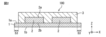
図1及び図2を参照しながら、第1実施形態に係る伸縮性デバイス100の構造について説明する。図1は、伸縮性デバイス100の上面図である。図2は、伸縮性デバイス100の図1におけるII-II断面図である。
(構造)
図1及び図2を参照しながら、第1実施形態に係る伸縮性デバイス100の構造について説明する。図1は、伸縮性デバイス100の上面図である。図2は、伸縮性デバイス100の図1におけるII-II断面図である。
伸縮性デバイス100は、伸縮性の第1基材1と、第1基材1の第1主面1a上に設けられた2本の配線2と、第1基材1の第1主面1aと配線2とを覆う保護層3とを備えている。伸縮性デバイス100は、例えば、プリント基板または、フレキシブル基板との回路接続に用いられる。なお、伸縮性デバイス100の形状は特に限定されない。
また、本明細書中における「上」とは、伸縮性デバイス100の使用時における上下と一致していなくてもよい。より具体的には、「第1基材1の主面上」とは、重力方向に規定される鉛直上方のような絶対的な一方向ではなく、第1基材1の主面を基準に、当該主面を境界とする外側と内側とのうち、外側に向かう方向を指す。また、ある要素に対して「上方(above)」には、当該要素とは離れた上方、すなわち当該要素上の他の物体を介した上側の位置や間隔を空けた上側の位置だけではなく、当該要素と接する直上の位置(on)も含む。
なお、図面に示すように、以下では、説明の便宜上、配線2の延在方向に直交する方向をX方向とする。配線2の延在方向をY方向とする。配線2の厚み方向をZ方向とする。X方向、Y方向及びZ方向は、互いに直交する方向であって、X,Y,Zの順に並べたとき、右手系を構成する。
第1基材1は、伸縮性を有する樹脂材料から構成されるフィルム材などの支持材である。第1基材1の形状はシート状またはフィルム状である。第1基材1は、互いに反対側に位置する第1主面1aと第2主面1bとを有する。
第1基材1は伸縮性を有する。第1基材1が伸縮性を有することで、配線2の伸縮を抑制せず、伸縮性デバイス100の使用時の伸縮における破断の危険性を低減することができる。第1基材1の厚さは特に限定されないが、生体に貼り付けた際に生体表面の伸縮を阻害しない観点からは、100μm以下であることが好ましく、1μm以下であることがより好ましい。第1基材1は、複数の層を積層したものであってもよい。
第1基材1の材料としては、例えば、熱可塑性樹脂などが挙げられる。具体的には伸縮性を有する樹脂材料、例えば、アクリル系樹脂、ウレタン系樹脂、及び、スチレン系樹脂からなる群より選択される少なくとも1種を含んでいる。ウレタン系樹脂としては、熱可塑性ポリウレタンを挙げることができる。スチレン系樹脂としては、スチレン-ブタジエン-スチレンブロック共重合体(SBS)を挙げることができる。
配線2は、互いに反対側に位置する第1面2aと第2面2bとを有する。配線2の第2面2bは、第1基材1の第1主面1a上に位置する。2本の配線2はX方向に沿って平行に並んで配置されている。なお、配線2の形状は特に限定されない。配線2はX方向とは異なる方向を向いて配置されてもよい。配線2の本数は特に限定されず、1本であってもよく、3本以上であってもよい。配線2は図1のような配置に限定されず、延伸方向も限定されない。具体的には、第1基材1の長手方向と配線2の延伸方向が一致していなくてもよいし、一方向に延伸していなくてもよい。
配線2は、好ましくは伸縮性を有する。配線2は、導電性材料で形成される。導電性材料には、例えば、銀、銅、ニッケルなどの金属箔を用いてもよく、銀、銅、ニッケルなどの導電性粒子と樹脂とからなる混合物を用いてもよい。樹脂としては、エポキシ樹脂、ウレタン系樹脂、アクリル系樹脂、シリコーン系樹脂など、或いはこれらの混合物であるエラストマー系樹脂を挙げることができる。このような樹脂を用いることにより、伸縮性を確保できる。導電性粒子の平均粒径は特に限定されるものではないが、0.01μm以上、10μm以下であることが好ましい。また、導電性粒子の形状は球形であることが好ましく、球形に限らず、伸縮性を良くするための扁平形や突起を有する構造でも良い。なお、配線2は、伸縮性を有していなくてもよい。
配線2の厚みは、好ましくは100μm以下であり、より好ましくは50μm以下である。また、伸縮性配線の厚みは、より好ましくは1μm以上であり、5μm以上であってもよい。なお、配線2の厚みや幅、長さは特に限定されない。
保護層3は、第1基材1の第1主面1aの一部及び配線2の全体を覆う。即ち、第1主面1aは、露出端部S3を有する。保護層3を設けることにより、配線2を保護することができる。なお、保護層3は、第1基材1の第1主面1aの少なくとも一部と配線2の少なくとも一部とを覆っていてもよい。保護層3は、単層であってもよく、複数の層が積層していてもよい。保護層3の材料は、第1基材1の材料と同一であってもよく、異なる材料であってもよい。
保護層3は、例えば、樹脂材料、又は、樹脂材料及び無機材料からなる混合物から形成される。樹脂材料として、例えば、シリコーン系樹脂、アクリル系樹脂、ポリエチレン、ポリプロピレン等のオレフィン系樹脂、変性ウレタン系樹脂、ウレタン系樹脂、スチレン系樹脂、塩化ビニル系樹脂、ポリエステル系樹脂、ポリアミド系樹脂を挙げることができる。また、樹脂材料として、フッ素系、ニトリルゴム、ラテックスゴム等のエラストマー系樹脂、エポキシ、フェノール、イミド系、ロジン、セルロース、ポリエチレンテレフタレート系、ポリエチレンナフタレート系、ポリカーボネート系樹脂を用いてもよい。なお、保護層3の材料は、第1基材の材料と同一であってもよい。保護層3は絶縁性を有することが好ましい。保護層3が絶縁性を有することで、配線2のイオンマイグレーションをより確実に抑制することができる。
保護層3は、例えば、絶縁ペーストを塗布して設けることができる。保護層3は、シート材を用いて設けることもできる。絶縁ペーストは、第1基材1の第1主面1aの一部と、配線層3上にスクリーン印刷、グラビア印刷、インクジェット印刷等により設けることができる。
保護層3の厚みは、1μm以上100μm以下であることが好ましく、50μm以下であってもよい。保護層3の厚みを1μm以上にすることで、保護層3の耐久性を確保することができる。また、保護層3の厚みを100μm以下にすることで、全体を低背化させることができる。なお、保護層3の厚みが一定でない場合、保護層3の厚みは、保護層3の最大の厚みとする。
配線2と第1基材1との間の剥離強度は、保護層3と第1基材1との間の剥離強度よりも大きい。伸縮性デバイス100に外力F1を付加した場合、保護層3と第1基材1との間に剥離が生じなければ、伸縮性デバイス100は均一に伸縮する。上記構成を有することにより、配線2と第1基材1との剥離よりも先に、保護層3と第1基材1とが剥離し、保護層3と第1基材1との間に剥離が生じると、剥離した箇所で外力F1を吸収できる。外力F1に対する配線2の負荷は低減され、配線2が第1基材1から剥離して断線することを抑制できる。
具体的に、伸縮性デバイス100を伸長する場合について、図2及び図3を用いて説明する。図2に示すように、伸縮性デバイス100において、第1基材1の第1主面1aに2本の配線2が位置し、保護層3が2本の配線2を覆うように第1主面1a上に設けられる。図3に示すように、配線2の延在方向に直交する断面において、この伸縮性デバイス100に、左右に伸長する外力F1を加える。外力F1を加えることにより、剥離強度の弱い箇所において剥離することがある。例えば、配線2と第1基材1との間よりも、2本の配線2間の第1基材1と保護層3において剥離し、空隙Sが生じることがある。第1主面1aは、配線2の延在方向に直交する断面において、X軸方向に、露出端部S3、保護層3と接触し、該露出端部S3に隣接する部分S4、配線2と接触し、該部分S4に隣接する部分S2、空隙Sと接触し、該部分S2と隣接する部分S1、配線2と接触し、該部分S1に隣接する部分S2、保護層3と接触し、該部分S2に隣接する部分S4、及び、該部分S4に隣接する露出端部S3を、順に有する。露出端部S3においては、第1基材1の第1主面1aは保護層3からの拘束が低減され、良好に伸長することができる。したがって、部分S1及び露出端部S3が大きく伸長することができ、外力F1を吸収できる。その結果、外力F1に対する配線2の負荷は低減され、配線2は第1基材1から剥離して断線することを抑制でき、配線2を保護できる。伸縮性デバイス100が縮む場合についても、伸長する場合と同様の作用効果が生じると考えられる。なお、図3では配線2の間の全ての領域が剥離し、空隙Sを備える場合を説明したが、配線2の間の一部のみが剥離していてもよい。換言すれば、相対的に剥離強度の低い部分は、保護層3と第1基材1とが接触する領域の全体である必要はなく、一部であってもよい。同様に、剥離強度の低い部分の場所は限定されず、配線2間以外の領域にあってもよい。
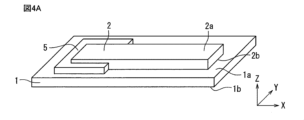
図4A、図4B、図4Cに、第1基材1と配線2との剥離強度の測定方法を記載する。定量的な界面剥離強度の測定方法として、JIS Z 0237 粘着テープの180°剥離試験、及び、JIS Z 0238 ヒートシール軟包装袋及び半剛性容器の試験方法を参考に、粘着テープの180°剥離試験を行った。図4Aに示すように、第1基材1の第1主面1a上に、導電性材料を塗布して配線2を形成する。第1基材1の第1主面1aと配線2の一方は、フッ素系樹脂などの離型フィルム5で離隔し、第1基材1の第1主面1aと配線2の他方は、接着する。なお、配線2は破断しやすいことから、配線2の第1面2a上にカプトンテープやコーティング剤等で補強してもよい。図4Bに示すように、離型フィルム5を除き、第1基材1と配線2とを、Y方向の幅Wが10mmである短冊状に切断する。図4Cに示すように、離隔している領域の一部にクランプ6を取りつける。クランプ6に、互いに離れる方向、即ち、180°離れた方向に引っ張る引張力F2を加え、剥離していく。剥離強度の測定には、フォースゲージを用いる。なお、第1基材1と保護層3との剥離強度の測定には、第1基材1と配線2との代わりに第1基材と保護層3とを用い、上記と同様の操作を行う。保護層3と配線2との剥離強度の測定には、第1基材1と配線2との代わりに保護層3と配線2とを用い、上記と同様の操作を行う。
好ましくは、保護層3は、シート層31である。例えば、導電性材料を塗布して保護層3を形成する場合、導電性材料中に溶剤が含まれると、配線2の少なくとも一部が溶解して、電気的な抵抗が生じることがある。これに対し、保護層3としてシート層31を用いると、配線2は溶解せず、電気的な抵抗は生じにくい。また、配線2と第1基材1間の剥離強度は低減されない。シート層31の形成は、配線2とシート層31との間に気泡が入らないように、真空状態において行うことが好ましい。この時、圧力と温度を加えながら張り合わせることが好ましい。シート層31の厚みは、好ましくは1μm以上100μm以下、より好ましくは10μm以上50μm以下である。
好ましくは、保護層3は、第1基材1の第1主面1aの一部を覆う。例えば、図1に示すように、第1基材1の第1主面1aは、配線2の延在する方向に平行に、一方の露出端部S3と、該露出端部S3に接触する保護層3及び配線2に接触する接触部と、該接触部に接触する他方の露出端部S3とを有する。露出端部S3は、配線2の延在する方向に平行な第1主面1aの端部である。外力F1を伸縮性デバイスに加えたときに、第1基材1の露出している部分である露出端部S3においても、第1基材1を大きく伸縮することができ、外力F1を吸収できる。これにより、配線2に応力が集中することを抑制できる。
好ましくは、保護層3と配線2との間の剥離強度は、保護層3と第1基材1との間の剥離強度よりも大きい。上記構成を有することにより、第1基材1に外力F1が付加したときに、保護層3と配線2とが剥離するより前に、保護層3と第1基材1とが剥離する。配線2と保護層3とは密着しているので、配線2と保護層3との間に隙間は生じず、配線2への応力集中を低減できる。
配線2と第1基材1との間の剥離強度は、配線2と保護層3との間の剥離強度よりも大きくてもよい。この場合、部分S1間に働く張力によって第1基材1から配線2が剥離することを抑制できる。
配線2と保護層3との間の剥離強度は、配線2と第1基材1との間の剥離強度よりも大きくてもよい。この場合、外力F1を付加する方向に直交する方向であって、図3において上下方向に外力が付加された際に、付加された外力は配線2の伸長を補助できる。その結果、配線2は均一に伸縮し、第1基材1から配線2が剥離することを抑制できる。
(製造方法)
伸縮性デバイスの製造方法について記載する。第1基材1として、例えばSBSを準備する。第1基材1の第1主面1aに、銀及び樹脂の混合物を含有する導電性材料を塗布する。なお、塗布の方法としては、例えば、スクリーン印刷、グラビア印刷、又は、インクジェット印刷を挙げることができる。導電性材料を、所定の抵抗値が得られるように熱硬化させることによって、配線2を形成する。配線2の硬化は、例えば80℃以上の温度において30分以上加熱することにより行う。配線2を設けた後、第1基材1の第1主面1aと配線2とを覆うように保護層3を設ける。
伸縮性デバイスの製造方法について記載する。第1基材1として、例えばSBSを準備する。第1基材1の第1主面1aに、銀及び樹脂の混合物を含有する導電性材料を塗布する。なお、塗布の方法としては、例えば、スクリーン印刷、グラビア印刷、又は、インクジェット印刷を挙げることができる。導電性材料を、所定の抵抗値が得られるように熱硬化させることによって、配線2を形成する。配線2の硬化は、例えば80℃以上の温度において30分以上加熱することにより行う。配線2を設けた後、第1基材1の第1主面1aと配線2とを覆うように保護層3を設ける。
[第2実施形態]
図5を参照しながら、第2実施形態に係る伸縮性デバイス100Aの構造について説明する。図5は、伸縮性デバイス100AのXY断面図である。第2実施形態は、第1実施形態と比較して、保護層の形状が異なる。
図5を参照しながら、第2実施形態に係る伸縮性デバイス100Aの構造について説明する。図5は、伸縮性デバイス100AのXY断面図である。第2実施形態は、第1実施形態と比較して、保護層の形状が異なる。
図5に示すように、保護層3Aは、配線2の延在する方向に直交する断面において、第1基材1側の下部3bと、第1基材1と反対側の上部3aと、下部3bと上部3aとを接続する幅方向の両側の凸曲面3cとを有し、下部3bの幅は、上部3aの幅よりも大きい。下部3bの幅が、上部3aの幅よりも大きくなることにより、保護層3の体積が小さくなり、コストを低減でき、伸縮性デバイス100Aをコンパクトにできる。また、凸曲部3cを有することにより、保護層3Aの上部3a側に角部が存在しなくなる。これにより、保護層3Aの損傷を避けることができる。なお、下部3bと上部3aとは、凸曲部3cでなく、平坦部で接続していてもよい。なお、本明細書中の下部3bの幅とは、図5で示しているように保護層3のうち第1基材1に接触している部分の幅と、配線2のうち第1基材1に接触している部分の幅を足し合わせたものである。
好ましくは、保護層3Aは、導電性材料を塗布して形成される。保護層3Aの厚みは、配線2の厚みよりも、好ましくは1μm以上10,000μm以下大きくする。保護層3Aの厚みは、好ましくは1μm以上100μm以下、より好ましくは10μm以上50μm以下である。
[第3実施形態]
図6を参照しながら、第3実施形態に係る伸縮性デバイス100Bの構造について説明する。図6は、伸縮性デバイス100Bの断面図である。第3実施形態は、第1実施形態と比較して、保護層の構成が異なる。
図6を参照しながら、第3実施形態に係る伸縮性デバイス100Bの構造について説明する。図6は、伸縮性デバイス100Bの断面図である。第3実施形態は、第1実施形態と比較して、保護層の構成が異なる。
図6に示すように、保護層3Bは、シート層31と接着剤層32とを有し、接着剤層32は、シート層31と配線2との間、及び、シート層31と第1基材1の第1主面1aとの間に位置する。上記態様を有することにより、保護層3と第1基材1との間の接着性や、保護層3と配線2との間の接着性を向上できる。また、保護層3Bの形成に導電性材料を用いる場合、導電性材料中に溶剤が含まれると、配線2の少なくとも一部が溶解して、電気的な抵抗が生じることがある。これに対し、シート層31と接着剤層32を有することにより、配線2は溶解されず、電気的な抵抗は生じない。配線2が溶解されないことから、配線2と保護層3との間の剥離強度は低減されない。接着剤層32としては、例えば、アクリル系粘着剤、シリコーン系粘着剤、ウレタン系粘着剤を挙げることができ、具体的にはアクリル系粘着剤を上げることができる。
[第4実施形態]
図7及び図8を参照しながら、第4実施形態に係る伸縮性デバイス100Cの構造について説明する。図7は、伸縮性デバイス100Cの上面図である。図8は、伸縮性デバイス100Cの図7におけるVIII-VIII断面図である。第4実施形態は、第1実施形態と比較して、保護層と第1基材との重複関係が異なる。
図7及び図8を参照しながら、第4実施形態に係る伸縮性デバイス100Cの構造について説明する。図7は、伸縮性デバイス100Cの上面図である。図8は、伸縮性デバイス100Cの図7におけるVIII-VIII断面図である。第4実施形態は、第1実施形態と比較して、保護層と第1基材との重複関係が異なる。
図7及び図8に示すように、保護層3Cは、第1基材1の第1主面1aの全体を覆う。即ち、第1主面1aは、露出端部を有しない。上記構成を有することにより、第1基材1において、部分的に応力が集中することを抑制できる。
[第5実施形態]
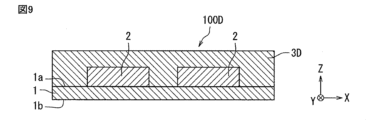
図9を参照しながら、第5実施形態に係る伸縮性デバイス100Dの構造について説明する。図9は、伸縮性デバイス100Dの断面図である。第5実施形態は、第4実施形態と比較して、保護層の構成が異なる。
図9を参照しながら、第5実施形態に係る伸縮性デバイス100Dの構造について説明する。図9は、伸縮性デバイス100Dの断面図である。第5実施形態は、第4実施形態と比較して、保護層の構成が異なる。
図9に示すように、保護層3Dの材料は、第1基材1の材料と同一の材料である。具体的には、一方の第1基材1上に配線2を設け、その後、配線2を覆うように他方の第1基材1を設け、一方の第1基材1と配線2とを全体に覆うように、他方の第1基材1を設ける。上記構成を有することにより、伸縮性デバイス100Dの伸縮性を向上できる。さらに、用いる材料の種類を削減でき、コストを低減できる。
[第6実施形態]
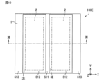
図10及び図11を参照しながら、第6実施形態に係る伸縮性デバイス100Eの構造について説明する。図10は、伸縮性デバイス100Eの上面図である。図11は、伸縮性デバイス100Eの図10におけるXI-XI断面図である。第6実施形態は、第1実施形態と比較して、保護層の個数が異なり、2本の配線間に第1主面の露出面が存在する。
図10及び図11を参照しながら、第6実施形態に係る伸縮性デバイス100Eの構造について説明する。図10は、伸縮性デバイス100Eの上面図である。図11は、伸縮性デバイス100Eの図10におけるXI-XI断面図である。第6実施形態は、第1実施形態と比較して、保護層の個数が異なり、2本の配線間に第1主面の露出面が存在する。
図10及び図11に示すように、保護層3Eは、配線2の全体を覆う。具体的には、第1基材1の第1主面1a上に、2つの配線2と、2つの保護層3Eとが位置し、一方の保護層3Eは一方の配線2を覆い、他方の保護層3Eは他方の配線2を覆う。一方の保護層3Eと、他方の保護層3Eとは離隔している。第1主面1aは、X軸方向に、露出端部S13、一方の保護層3Eと接触し、該露出端部S13に隣接する部分S12、該部分S12に隣接する露出部S11、他方の保護層3Eと接触し、該露出部S11に隣接する部分S12、及び、該部分S12に隣接する露出端部S13を、順に有する。本実施形態において、部分S12には保護層3Eが配置されていないため、保護層3Eによって拘束されない部分の面積を確保することができ、より好適に外力の影響を緩和させることができる。
さらに、本実施形態においては、部分S12のうち、第1基材1と保護層3Eとが直接接触している部分S15及びS16の剥離強度は、第1基材1と配線2とが直接接触している部分S14の剥離強度より相対的に低い。したがって、部分S12において、部分S15及びS16は、部分S14よりも第1基材1から剥離しやすい。さらに、部分S15が配線2間に位置するため、部分S15は、部分S16よりも第1基材1から剥離しやすい。このことから、伸縮性デバイス100Eが伸縮すると、部分S15が第1基材1から剥離することがある。即ち、本実施形態においては、部分S15を有することによって、剥離強度をコントロールできる。
なお、本構成において、伸縮によって生じた空隙(部分S15と第1基材1との剥離により生じた空隙)は、露出部S11と一体化されていてもよいし、一体化されていなくてもよい。具体的には、露出部S11と部分S15とが一体化される場合とは、部分S15の全体が剥離した場合、又は、部分S15の露出部S11側の領域が剥離した場合である。露出部S11と部分S11とが一体化されない場合とは、部分S15において、露出部S11側以外の領域が剥離した場合である。例えば、部分S15の部分S14側の領域が剥離する場合等が考えられる。
なお、本開示は上述の実施形態に限定されず、本開示の要旨を逸脱しない範囲で設計変更可能である。例えば、第1から第6実施形態のそれぞれの特徴点を様々に組み合わせてもよい。
本開示は、下記の態様を含む。
<1>
第1主面を有する伸縮性の第1基材と、
前記第1基材の前記第1主面上に設けられた配線と、
前記第1基材の前記第1主面の少なくとも一部と前記配線の少なくとも一部とを覆う保護層と、
を備え、
前記配線と前記第1基材との間の剥離強度は、前記保護層と前記第1基材との間の剥離強度よりも大きい、
伸縮性デバイス。
<2>
前記保護層は、前記配線の延在方向に直交する断面において、前記第1基材側の下部と、前記第1基材と反対側の上部と、前記下部と前記上部とを接続する幅方向の両側の凸曲面とを有し、
前記下部の幅は、前記上部の幅よりも大きい、
<1>に記載の伸縮性デバイス。
<3>
前記保護層は、シート層と接着剤層とを有し、
前記接着剤層は、前記配線と前記シート層との間、及び、前記第1基材の前記第1主面と前記シート層との間に位置する、
<1>に記載の伸縮性デバイス。
<4>
前記保護層は、シート層であって、前記配線を設けた前記第1基材の前記第1主面と接触する、
<1>に記載の伸縮性デバイス。
<5>
前記保護層は、前記第1基材の前記第1主面の全体を覆う、<1>から<4>の何れか1つに記載の伸縮性デバイス。
<6>
前記保護層は、前記第1基材の前記第1主面の一部を覆う、<1>から<4>の何れか1つに記載の伸縮性デバイス。
<7>
前記保護層の材料は、前記第1基材の材料と同一の材料である、
<1>から<6>の何れか1つに記載の伸縮性デバイス。
<8>
前記保護層は、前記配線の全体を覆う、<1>から<7>の何れか1つに記載の伸縮性デバイス。
<9>
前記保護層と前記配線との間の剥離強度は、前記保護層と前記第1基材との間の剥離強度よりも大きい、<1>から<8>の何れか1つに記載の伸縮性デバイス。
<1>
第1主面を有する伸縮性の第1基材と、
前記第1基材の前記第1主面上に設けられた配線と、
前記第1基材の前記第1主面の少なくとも一部と前記配線の少なくとも一部とを覆う保護層と、
を備え、
前記配線と前記第1基材との間の剥離強度は、前記保護層と前記第1基材との間の剥離強度よりも大きい、
伸縮性デバイス。
<2>
前記保護層は、前記配線の延在方向に直交する断面において、前記第1基材側の下部と、前記第1基材と反対側の上部と、前記下部と前記上部とを接続する幅方向の両側の凸曲面とを有し、
前記下部の幅は、前記上部の幅よりも大きい、
<1>に記載の伸縮性デバイス。
<3>
前記保護層は、シート層と接着剤層とを有し、
前記接着剤層は、前記配線と前記シート層との間、及び、前記第1基材の前記第1主面と前記シート層との間に位置する、
<1>に記載の伸縮性デバイス。
<4>
前記保護層は、シート層であって、前記配線を設けた前記第1基材の前記第1主面と接触する、
<1>に記載の伸縮性デバイス。
<5>
前記保護層は、前記第1基材の前記第1主面の全体を覆う、<1>から<4>の何れか1つに記載の伸縮性デバイス。
<6>
前記保護層は、前記第1基材の前記第1主面の一部を覆う、<1>から<4>の何れか1つに記載の伸縮性デバイス。
<7>
前記保護層の材料は、前記第1基材の材料と同一の材料である、
<1>から<6>の何れか1つに記載の伸縮性デバイス。
<8>
前記保護層は、前記配線の全体を覆う、<1>から<7>の何れか1つに記載の伸縮性デバイス。
<9>
前記保護層と前記配線との間の剥離強度は、前記保護層と前記第1基材との間の剥離強度よりも大きい、<1>から<8>の何れか1つに記載の伸縮性デバイス。
本願は、2023年6月5日付けで日本国に出願された特願2023-092419に基づく優先権を主張し、その記載内容の全てが、参照することにより本明細書に援用される。
100,100A,100B,100C,100D,100E 伸縮性デバイス
1 第1基材
1a 第1主面
2 配線
3,3A,3B,3C,3D,3E 保護層
3a 上部
3b 下部
3c 凸曲部
31 シート層
32 接着剤層
1 第1基材
1a 第1主面
2 配線
3,3A,3B,3C,3D,3E 保護層
3a 上部
3b 下部
3c 凸曲部
31 シート層
32 接着剤層
Claims (9)
- 第1主面を有する伸縮性の第1基材と、
前記第1基材の前記第1主面上に設けられた配線と、
前記第1基材の前記第1主面の少なくとも一部と前記配線の少なくとも一部とを覆う保護層と、
を備え、
前記配線と前記第1基材との間の剥離強度は、前記保護層と前記第1基材との間の剥離強度よりも大きい、
伸縮性デバイス。 - 前記保護層は、前記配線の延在方向に直交する断面において、前記第1基材側の下部と、前記第1基材と反対側の上部と、前記下部と前記上部とを接続する幅方向の両側の凸曲面とを有し、
前記下部の幅は、前記上部の幅よりも大きい、
請求項1に記載の伸縮性デバイス。 - 前記保護層は、シート層と接着剤層とを有し、
前記接着剤層は、前記配線と前記シート層との間、及び、前記第1基材の前記第1主面と前記シート層との間に位置する、
請求項1に記載の伸縮性デバイス。 - 前記保護層は、シート層であって、前記配線を設けた前記第1基材の前記第1主面と接触する、
請求項1に記載の伸縮性デバイス。 - 前記保護層は、前記第1基材の前記第1主面の全体を覆う、請求項1から4の何れか1項に記載の伸縮性デバイス。
- 前記保護層は、前記第1基材の前記第1主面の一部を覆う、請求項1から4の何れか1項に記載の伸縮性デバイス。
- 前記保護層の材料は、前記第1基材の材料と同一の材料である、
請求項1から6の何れか1項に記載の伸縮性デバイス。 - 前記保護層は、前記配線の全体を覆う、請求項1から7の何れか1項に記載の伸縮性デバイス。
- 前記保護層と前記配線との間の剥離強度は、前記保護層と前記第1基材との間の剥離強度よりも大きい、請求項1から8の何れか1項に記載の伸縮性デバイス。
Priority Applications (1)
| Application Number | Priority Date | Filing Date | Title |
|---|---|---|---|
| JP2025525978A JPWO2024252805A1 (ja) | 2023-06-05 | 2024-04-22 |
Applications Claiming Priority (2)
| Application Number | Priority Date | Filing Date | Title |
|---|---|---|---|
| JP2023-092419 | 2023-06-05 | ||
| JP2023092419 | 2023-06-05 |
Publications (1)
| Publication Number | Publication Date |
|---|---|
| WO2024252805A1 true WO2024252805A1 (ja) | 2024-12-12 |
Family
ID=93795371
Family Applications (1)
| Application Number | Title | Priority Date | Filing Date |
|---|---|---|---|
| PCT/JP2024/015712 Ceased WO2024252805A1 (ja) | 2023-06-05 | 2024-04-22 | 伸縮性デバイス |
Country Status (2)
| Country | Link |
|---|---|
| JP (1) | JPWO2024252805A1 (ja) |
| WO (1) | WO2024252805A1 (ja) |
Citations (3)
| Publication number | Priority date | Publication date | Assignee | Title |
|---|---|---|---|---|
| WO2019012909A1 (ja) * | 2017-07-14 | 2019-01-17 | ソニー株式会社 | センサおよびセンサの製造方法 |
| WO2019097860A1 (ja) * | 2017-11-17 | 2019-05-23 | 東洋紡株式会社 | 生体情報計測用衣服および伸縮性積層シート |
| WO2020013323A1 (ja) * | 2018-07-13 | 2020-01-16 | 東洋紡株式会社 | 衣服型電子機器およびその製造方法 |
-
2024
- 2024-04-22 WO PCT/JP2024/015712 patent/WO2024252805A1/ja not_active Ceased
- 2024-04-22 JP JP2025525978A patent/JPWO2024252805A1/ja active Pending
Patent Citations (3)
| Publication number | Priority date | Publication date | Assignee | Title |
|---|---|---|---|---|
| WO2019012909A1 (ja) * | 2017-07-14 | 2019-01-17 | ソニー株式会社 | センサおよびセンサの製造方法 |
| WO2019097860A1 (ja) * | 2017-11-17 | 2019-05-23 | 東洋紡株式会社 | 生体情報計測用衣服および伸縮性積層シート |
| WO2020013323A1 (ja) * | 2018-07-13 | 2020-01-16 | 東洋紡株式会社 | 衣服型電子機器およびその製造方法 |
Also Published As
| Publication number | Publication date |
|---|---|
| JPWO2024252805A1 (ja) | 2024-12-12 |
Similar Documents
| Publication | Publication Date | Title |
|---|---|---|
| KR102839087B1 (ko) | 플렉서블 표시장치 | |
| US10470304B2 (en) | Flexible electronics apparatus and associated methods | |
| EP3223120B1 (en) | Film touch sensor and manufacturing method therefor | |
| CN103153811B (zh) | 覆盖膜 | |
| CN116419613A (zh) | 显示装置 | |
| WO2017173872A1 (zh) | 胶材组件、柔性模组、显示设备及柔性模组的制作方法 | |
| JP5111071B2 (ja) | 圧電センサ | |
| WO2018142879A1 (ja) | 熱伝導シートおよび多重熱伝導シート | |
| TW200832659A (en) | Semiconductor device, stacked semiconductor device and interposer substrate | |
| JP2024033004A (ja) | センサ及びその製造方法 | |
| JP2021123419A (ja) | 電子部品包装用カバーテープ、電子部品包装体およびその製造方法 | |
| KR101899831B1 (ko) | 플렉서블 표시장치 | |
| KR20170029920A (ko) | 더미를 이용하여 강성 조절되는 연성 반도체 기판, 및 연성 반도체 패키지 | |
| JP7718604B2 (ja) | 伸縮性デバイス | |
| KR20180043872A (ko) | 반도체 칩, 이를 구비한 전자장치 및 반도체 칩의 연결방법 | |
| TW202016612A (zh) | 觸控結構及觸控裝置 | |
| JP2020170754A (ja) | 複合基板及びその製造方法 | |
| JPH10250020A (ja) | トップカバーテープ | |
| WO2025192170A1 (ja) | 伸縮性デバイス | |
| JP6691474B2 (ja) | 伸縮性配線基板及び伸縮性基板の製造方法 | |
| US20240357738A1 (en) | Stretchable wiring board | |
| US20250203765A1 (en) | Stretchable device | |
| US20250227846A1 (en) | Wiring board | |
| CN113785027A (zh) | 粘接剂组合物 | |
| JP2025163606A (ja) | 伸縮性を有する半導体装置及び半導体システム |
Legal Events
| Date | Code | Title | Description |
|---|---|---|---|
| 121 | Ep: the epo has been informed by wipo that ep was designated in this application |
Ref document number: 24819043 Country of ref document: EP Kind code of ref document: A1 |
|
| ENP | Entry into the national phase |
Ref document number: 2025525978 Country of ref document: JP Kind code of ref document: A |
|
| WWE | Wipo information: entry into national phase |
Ref document number: 2025525978 Country of ref document: JP |
|
| NENP | Non-entry into the national phase |
Ref country code: DE |