WO2024252821A1 - Power storage device - Google Patents
Power storage device Download PDFInfo
- Publication number
- WO2024252821A1 WO2024252821A1 PCT/JP2024/016333 JP2024016333W WO2024252821A1 WO 2024252821 A1 WO2024252821 A1 WO 2024252821A1 JP 2024016333 W JP2024016333 W JP 2024016333W WO 2024252821 A1 WO2024252821 A1 WO 2024252821A1
- Authority
- WO
- WIPO (PCT)
- Prior art keywords
- conductive
- foil
- current collecting
- adhesive layer
- current collector
- Prior art date
- Legal status (The legal status is an assumption and is not a legal conclusion. Google has not performed a legal analysis and makes no representation as to the accuracy of the status listed.)
- Ceased
Links
Images



Classifications
-
- H—ELECTRICITY
- H01—ELECTRIC ELEMENTS
- H01M—PROCESSES OR MEANS, e.g. BATTERIES, FOR THE DIRECT CONVERSION OF CHEMICAL ENERGY INTO ELECTRICAL ENERGY
- H01M10/00—Secondary cells; Manufacture thereof
- H01M10/04—Construction or manufacture in general
- H01M10/0413—Large-sized flat cells or batteries for motive or stationary systems with plate-like electrodes
- H01M10/0418—Large-sized flat cells or batteries for motive or stationary systems with plate-like electrodes with bipolar electrodes
-
- H—ELECTRICITY
- H01—ELECTRIC ELEMENTS
- H01G—CAPACITORS; CAPACITORS, RECTIFIERS, DETECTORS, SWITCHING DEVICES, LIGHT-SENSITIVE OR TEMPERATURE-SENSITIVE DEVICES OF THE ELECTROLYTIC TYPE
- H01G11/00—Hybrid capacitors, i.e. capacitors having different positive and negative electrodes; Electric double-layer [EDL] capacitors; Processes for the manufacture thereof or of parts thereof
- H01G11/10—Multiple hybrid or EDL capacitors, e.g. arrays or modules
- H01G11/12—Stacked hybrid or EDL capacitors
-
- H—ELECTRICITY
- H01—ELECTRIC ELEMENTS
- H01G—CAPACITORS; CAPACITORS, RECTIFIERS, DETECTORS, SWITCHING DEVICES, LIGHT-SENSITIVE OR TEMPERATURE-SENSITIVE DEVICES OF THE ELECTROLYTIC TYPE
- H01G11/00—Hybrid capacitors, i.e. capacitors having different positive and negative electrodes; Electric double-layer [EDL] capacitors; Processes for the manufacture thereof or of parts thereof
- H01G11/66—Current collectors
- H01G11/68—Current collectors characterised by their material
-
- H—ELECTRICITY
- H01—ELECTRIC ELEMENTS
- H01G—CAPACITORS; CAPACITORS, RECTIFIERS, DETECTORS, SWITCHING DEVICES, LIGHT-SENSITIVE OR TEMPERATURE-SENSITIVE DEVICES OF THE ELECTROLYTIC TYPE
- H01G11/00—Hybrid capacitors, i.e. capacitors having different positive and negative electrodes; Electric double-layer [EDL] capacitors; Processes for the manufacture thereof or of parts thereof
- H01G11/66—Current collectors
- H01G11/70—Current collectors characterised by their structure
-
- H—ELECTRICITY
- H01—ELECTRIC ELEMENTS
- H01M—PROCESSES OR MEANS, e.g. BATTERIES, FOR THE DIRECT CONVERSION OF CHEMICAL ENERGY INTO ELECTRICAL ENERGY
- H01M4/00—Electrodes
- H01M4/02—Electrodes composed of, or comprising, active material
- H01M4/64—Carriers or collectors
- H01M4/66—Selection of materials
- H01M4/665—Composites
- H01M4/667—Composites in the form of layers, e.g. coatings
-
- H—ELECTRICITY
- H01—ELECTRIC ELEMENTS
- H01M—PROCESSES OR MEANS, e.g. BATTERIES, FOR THE DIRECT CONVERSION OF CHEMICAL ENERGY INTO ELECTRICAL ENERGY
- H01M4/00—Electrodes
- H01M4/02—Electrodes composed of, or comprising, active material
- H01M4/64—Carriers or collectors
- H01M4/66—Selection of materials
- H01M4/668—Composites of electroconductive material and synthetic resins
-
- H—ELECTRICITY
- H01—ELECTRIC ELEMENTS
- H01M—PROCESSES OR MEANS, e.g. BATTERIES, FOR THE DIRECT CONVERSION OF CHEMICAL ENERGY INTO ELECTRICAL ENERGY
- H01M4/00—Electrodes
- H01M4/02—Electrodes composed of, or comprising, active material
- H01M2004/026—Electrodes composed of, or comprising, active material characterised by the polarity
- H01M2004/029—Bipolar electrodes
-
- H—ELECTRICITY
- H01—ELECTRIC ELEMENTS
- H01M—PROCESSES OR MEANS, e.g. BATTERIES, FOR THE DIRECT CONVERSION OF CHEMICAL ENERGY INTO ELECTRICAL ENERGY
- H01M2220/00—Batteries for particular applications
- H01M2220/20—Batteries in motive systems, e.g. vehicle, ship, plane
-
- Y—GENERAL TAGGING OF NEW TECHNOLOGICAL DEVELOPMENTS; GENERAL TAGGING OF CROSS-SECTIONAL TECHNOLOGIES SPANNING OVER SEVERAL SECTIONS OF THE IPC; TECHNICAL SUBJECTS COVERED BY FORMER USPC CROSS-REFERENCE ART COLLECTIONS [XRACs] AND DIGESTS
- Y02—TECHNOLOGIES OR APPLICATIONS FOR MITIGATION OR ADAPTATION AGAINST CLIMATE CHANGE
- Y02E—REDUCTION OF GREENHOUSE GAS [GHG] EMISSIONS, RELATED TO ENERGY GENERATION, TRANSMISSION OR DISTRIBUTION
- Y02E60/00—Enabling technologies; Technologies with a potential or indirect contribution to GHG emissions mitigation
- Y02E60/10—Energy storage using batteries
-
- Y—GENERAL TAGGING OF NEW TECHNOLOGICAL DEVELOPMENTS; GENERAL TAGGING OF CROSS-SECTIONAL TECHNOLOGIES SPANNING OVER SEVERAL SECTIONS OF THE IPC; TECHNICAL SUBJECTS COVERED BY FORMER USPC CROSS-REFERENCE ART COLLECTIONS [XRACs] AND DIGESTS
- Y02—TECHNOLOGIES OR APPLICATIONS FOR MITIGATION OR ADAPTATION AGAINST CLIMATE CHANGE
- Y02P—CLIMATE CHANGE MITIGATION TECHNOLOGIES IN THE PRODUCTION OR PROCESSING OF GOODS
- Y02P70/00—Climate change mitigation technologies in the production process for final industrial or consumer products
- Y02P70/50—Manufacturing or production processes characterised by the final manufactured product
Definitions
- This disclosure relates to an electricity storage device.
- An example of a conventional power storage device is the bipolar battery described in Patent Document 1.
- This conventional bipolar battery has multiple bipolar electrodes, each of which has a positive electrode active material layer formed on one side of a current collector and a negative electrode active material layer formed on the other side.
- the bipolar battery is constructed by stacking these bipolar electrodes with a gel electrolyte layer sandwiched between them.
- a structure in which metal foils of different materials are laminated together via a conductive adhesive may be used.
- the conductive adhesive may be, for example, a thermosetting resin that is the main component of the adhesive, in which a particulate conductive assistant (conductive particles) such as a conductive filler is dispersed.
- a particulate conductive assistant conductive particles
- Carbon black is a widely known example of a conductive assistant.
- a conductive adhesive using carbon black as a conductive assistant is used to bond laminated foils, in order to sufficiently reduce the resistance value of the laminated foils, it is necessary to include a large amount of carbon black in the conductive adhesive. In this case, a problem occurs in that the adhesive strength of the laminated foils decreases.
- the present disclosure aims to provide an energy storage device equipped with a bipolar electrode having a laminated foil that exhibits good bonding strength and good electrical conductivity.
- the energy storage device is an energy storage device including a plurality of bipolar electrodes overlapping each other in the stacking direction, each of the plurality of bipolar electrodes including a first current collecting foil and a second current collecting foil overlapping each other in the stacking direction, a conductive adhesive layer located between the first current collecting foil and the second current collecting foil and bonded to the first current collecting foil and the second current collecting foil, a first active material layer located on the surface of the first current collecting foil, and a second active material layer located on the surface of the second current collecting foil, the conductive adhesive layer includes an adhesive and a conductive assistant dispersed in the adhesive, the conductive assistant is a spherical particle having a spherical core and a conductive film covering the core, the conductive assistant is added at a rate of 0.1% by volume or more and 1.0% by volume or less, and a first value obtained by adding twice the standard deviation of the particle size of the conductive assistant to the average particle size of the conductive assistant is equal to or more
- each of the bipolar electrodes has a laminated foil in which a first current collecting foil and a second current collecting foil are bonded to each other via a conductive adhesive layer.
- the conductive assistant dispersed in the adhesive in the conductive adhesive layer is a spherical particle having a spherical core and a conductive film covering the core, the conductive assistant is added at a rate of 0.1% by volume to 1.0% by volume, and a first value obtained by adding twice the standard deviation of the particle size of the conductive assistant to the average particle size of the conductive assistant is equal to or greater than the thickness of the conductive adhesive layer.
- the above-mentioned power storage device can be provided with a bipolar electrode that exhibits good bonding strength and conductivity.
- the average particle size of the conductive additive may be larger than the thickness of the conductive adhesive layer. In this case, better electrical conduction between the first current collecting foil and the second current collecting foil is achieved via the conductive additive.
- the first current collecting foil and the second current collecting foil each have a rectangular shape, the length of one side of the first current collecting foil and the length of one side of the second current collecting foil each are 500 mm or more, and the CV value of the particle size of the conductive assistant in the conductive adhesive layer may be 10% or less.
- the conductive assistant having a particle size significantly larger than the thickness of the conductive adhesive layer is unlikely to be present in the conductive adhesive layer.
- the resistance of the bipolar electrode is unlikely to increase due to deformation of the first current collecting foil and/or the second current collecting foil due to the air.
- each of the first current collecting foil and the second current collecting foil can be well bonded to the conductive adhesive layer.
- the first current collecting foil and the second current collecting foil each have a rectangular shape, and the length of one side of the first current collecting foil and the length of one side of the second current collecting foil are each 500 mm or more, and the second value obtained by adding the average particle size of the conductive assistant to three times the standard deviation may be equal to or less than twice the thickness of the conductive adhesive layer.
- a conductive assistant having a particle size significantly larger than the thickness of the conductive adhesive layer is unlikely to be present in the conductive adhesive layer.
- the bipolar electrode is enlarged, air is unlikely to be trapped between the first current collecting foil and the second current collecting foil due to the conductive assistant.
- each of the first current collecting foil and the second current collecting foil can be well bonded to the conductive adhesive layer.
- the thickness of the first current collecting foil is at least twice the thickness of the second current collecting foil, the thickness of the second current collecting foil is less than 10 ⁇ m, the thickness of the conductive adhesive layer is less than the thickness of the second current collecting foil, and the CV value of the particle size of the conductive additive in the conductive adhesive layer may be 10% or less.
- conductive additives having particle sizes significantly larger than the thickness of the conductive adhesive layer are unlikely to be present in the conductive adhesive layer. This makes it difficult for air to be trapped between the first current collecting foil and the second current collecting foil due to the conductive additive. This makes it difficult for the resistance of the bipolar electrode to increase due to deformation of the current collecting foil (especially the second current collecting foil) due to the air.
- the conductive adhesive layer may further contain an epoxy-based hardener as a hardener, in addition to the olefin-based adhesive as an adhesive.
- the adhesive can exhibit high electrolyte resistance, and therefore good bonding strength can be exhibited over a long period of time.
- an epoxy-based hardener as a hardener when an olefin-based adhesive is used as an adhesive, gas generation during the hardening reaction between the adhesive and hardener that occurs during the production of the current collector can be effectively reduced.
- an electricity storage device that has a laminated foil in which multiple metal foils are bonded together via a conductive adhesive, and that is equipped with a bipolar electrode current collector that exhibits good bonding strength and good electrical conductivity.
- FIG. 1 is a schematic cross-sectional view showing an electricity storage device according to one embodiment.
- FIG. 2 is an enlarged view of a main portion of FIG.
- FIG. 3A is an enlarged cross-sectional view of a main portion of a current collector
- FIG. 3B is an enlarged cross-sectional view of a conductive assistant.
- FIG. 4 is a schematic diagram showing a coating device used in the production of a current collector.
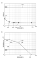
- FIG. 5(a) is a diagram showing the particle size distribution of the first conductive assistant dispersed in the conductive adhesive layer
- FIG. 5(b) is a diagram showing the relationship between the thickness of the conductive adhesive layer and the resistance value of the sample.
- FIG. 8 shows the particle size distribution of the second conductive assistant contained in the 11th sample and the 12th sample.
- FIG. 1 is a schematic cross-sectional view showing an energy storage device according to one embodiment.
- FIG. 2 is an enlarged view of a main portion of FIG. 1.
- the energy storage device 1 shown in FIG. 1 is a device (vehicle energy storage battery) used in batteries of various vehicles such as forklifts, hybrid cars, and electric cars.
- the energy storage device 1 is a secondary battery such as a nickel-metal hydride secondary battery or a lithium-ion secondary battery.
- the energy storage device 1 may be an electric double layer capacitor or an all-solid-state battery. The following describes an example in which the energy storage device 1 is a lithium-ion secondary battery.
- the energy storage device 1 comprises an electrode stack 2, which is a stack of multiple bipolar electrodes 14, and a sealing body 3 that seals the side surfaces 2a of the electrode stack 2 that extend in the stacking direction D of the bipolar electrodes 14. For this reason, the energy storage device 1 is also called a vehicle bipolar battery.
- the electrode stack 2 comprises multiple cells 4. Each cell 4 has a positive electrode 11, a negative electrode 12, and a separator 13.
- the positive electrode 11 and the negative electrode 12 are, for example, rectangular when viewed from the stacking direction D.
- the positive electrode 11 and the negative electrode 12 are arranged facing each other with the separator 13 in between.
- the facing direction of the positive electrode 11 and the negative electrode 12 coincides with the stacking direction D of the bipolar electrode 14.
- the positive electrode 11 is composed of a current collector 21 and a positive electrode active material layer 23 provided on a first surface 21a of the current collector 21.
- the negative electrode 12 is composed of a current collector 21 and a negative electrode active material layer 24 provided on a second surface 21b of the current collector 21.
- FIG. 3 is an enlarged cross-sectional view of a main part of the current collector.
- the current collector 21 is a chemically inactive electrical conductor for continuing to pass current to the positive electrode active material layer 23 and the negative electrode active material layer 24 during discharging or charging of the lithium ion secondary battery, and is a member (bipolar electrode current collector) used in the bipolar electrode 14.
- the current collector 21 has a three-layer structure having a first current collector foil 21A, a second current collector foil 21B, and a conductive adhesive layer 22 located between the first current collector foil 21A and the second current collector foil 21B and bonding the first current collector foil 21A and the second current collector foil 21B.
- Each of the first current collecting foil 21A and the second current collecting foil 21B is a conductive member having, for example, a rectangular shape when viewed from the stacking direction D.
- the first current collecting foil 21A and the second current collecting foil 21B are integrated with each other via the conductive adhesive layer 22.
- the first current collecting foil 21A and the second current collecting foil 21B overlapping each other along the stacking direction D are electrically connected to each other via the conductive adhesive layer 22.
- the first surface 21Aa of the first current collecting foil 21A is an exposed surface (surface) located on the opposite side to the surface in contact with the conductive adhesive layer 22, and corresponds to the first surface 21a of the current collector 21.
- the second surface 21Ab of the first current collecting foil 21A is a surface bonded to the conductive adhesive layer 22.
- the first surface 21Ba of the second current collecting foil 21B is an exposed surface (surface) located on the opposite side to the surface in contact with the conductive adhesive layer 22, and corresponds to the second surface 21b of the current collector 21.
- the second surface 21Bb of the second current collecting foil 21B is the surface that is bonded to the conductive adhesive layer 22.
- the length of one side of the first current collecting foil 21A and the length of one side of the second current collecting foil 21B are each 500 mm or more. The length may be 750 mm or more, 1000 mm or more, or 1200 mm or more.
- each cell 4 included in the electrode stack 2 the positive electrode 11 is composed of a portion of a specific bipolar electrode 14, and the negative electrode 12 is composed of a portion of another bipolar electrode 14.
- a plurality of cells 4 are formed by alternately stacking bipolar electrodes 14 and separators 13. Thus, a plurality of cells 4 are electrically connected in series.
- the same bipolar electrode 14 may be shared between adjacent cells 4, 4 in the stacking direction D.
- a terminal electrode (positive terminal electrode) including a first current collecting foil 21A is disposed.
- a terminal electrode (negative terminal electrode) including a second current collecting foil 21B is disposed.
- the first current collecting foil 21A and the second current collecting foil 21B may be formed, for example, in a plate-like, foil-like, sheet-like, film-like, or other form.
- first current collecting foil 21A and the second current collecting foil 21B are metal foils, for example, aluminum foil, copper foil, nickel foil, titanium foil, or stainless steel foil is used.
- the first current collecting foil 21A is, for example, an aluminum foil.
- the second current collecting foil 21B is, for example, a copper foil.
- the first current collecting foil 21A and the second current collecting foil 21B may be an alloy foil or clad foil of the above metals.
- the thickness of the first current collecting foil 21A and the second current collecting foil 21B along the stacking direction D may each be in the range of 1 ⁇ m to 150 ⁇ m. From the viewpoint of durability of the current collector 21, at least one of the thicknesses of the first current collector foil 21A and the second current collector foil 21B may be 50 ⁇ m or more, 40 ⁇ m or more, or 30 ⁇ m or more.
- the thickness of one of the first current collector foil 21A and the second current collector foil 21B is, for example, 1 ⁇ m or more and less than 10 ⁇ m, and the thickness of the other is, for example, 20 ⁇ m or more and 150 ⁇ m or less.
- one of the first current collector foil 21A and the second current collector foil 21B is a thin current collector foil with a thickness of less than 10 ⁇ m
- the other of the first current collector foil 21A and the second current collector foil 21B is a current collector foil having a thickness at least twice that of the thin current collector foil.
- the first current collecting foil 21A is an aluminum foil
- the second current collecting foil 21B is a copper foil.
- the aluminum foil of the first current collecting foil 21A and the copper foil of the second current collecting foil 21B are integrated by bonding via the conductive adhesive layer 22. Therefore, the current collector 21 can be said to be a foil (laminate foil) in which the first current collecting foil 21A and the second current collecting foil 21B are bonded to each other via the conductive adhesive layer 22. From the viewpoints of cost, weight, etc., the thickness of the first current collecting foil 21A in the current collector 21 is greater than the thickness of the second current collecting foil 21B.
- the thickness of the first current collecting foil 21A included in the bipolar electrode 14 is, for example, 40 ⁇ m or more and 100 ⁇ m or less. From the viewpoint of the strength of the current collector 21, the thickness of the first current collecting foil 21A may be five times or more the thickness of the second current collecting foil 21B. In this case, for example, even if the thickness of the second current collector foil 21B is 9 ⁇ m or less, the thickness of the first current collector foil 21A can be 45 ⁇ m or more, so that the strength of the current collector 21 can be sufficient as a laminated foil.
- the thickness of the second current collector foil 21B included in the bipolar electrode 14 is, for example, 5 ⁇ m or more and less than 10 ⁇ m.
- the thickness of the first current collector foil 21A included in the positive terminal electrode constituting the outermost electrode of the electrode laminate 2 may be 100 ⁇ m or more and 150 ⁇ m or less.
- the same laminated foil as the current collector 21 is used as the negative terminal electrode constituting the outermost electrode of the electrode laminate 2.
- the thickness of the first current collector foil included in the negative terminal electrode may be 100 ⁇ m or more and 150 ⁇ m or less. In other words, by making the first current collector foil thick, the thin second current collector foil can be reinforced.
- the conductive adhesive layer 22 is an anisotropic conductive member that bonds the first current collector foil 21A and the second current collector foil 21B to integrate them with each other, and is located between the first current collector foil 21A and the second current collector foil 21B in the stacking direction D.
- the conductive adhesive layer 22 is a member that electrically connects the first current collector foil 21A and the second current collector foil 21B to each other. From the viewpoints of ensuring the bonding strength between the first current collector foil 21A and the second current collector foil 21B, reducing the internal resistance of the current collector 21, and reducing the thickness of the current collector 21, the thickness TH of the conductive adhesive layer 22 is, for example, 2 ⁇ m or more and 5 ⁇ m or less.
- the conductive adhesive layer 22 has an adhesive 40 and a plurality of conductive assistants 50 dispersed in the adhesive 40.
- the adhesive 40 includes a resin that exhibits adhesiveness to both the first current collecting foil 21A and the second current collecting foil 21B.
- the resin include olefin-based resins such as polyethylene, polypropylene, and polybutylene, ethylene-vinyl acetate copolymer (EVA), polyethylene terephthalate (PET), polyethylene naphthalate (PEN), polyethernitrile (PEN), polyimide (PI), polyamide (PA), polytetrafluoroethylene (PTFE), styrene-butadiene rubber (SBR), polyacrylonitrile (PAN), polymethyl acrylate (PMA), polymethyl methacrylate (PMMA), polyvinyl chloride (PVC), polyvinylidene fluoride (PVDF), silicone, epoxy resin, or a mixture thereof.
- olefin-based resins such as polyethylene, polypropylene, and polybutylene, ethylene-vinyl acetate copolymer (EVA), polyethylene
- the above-mentioned resin may be an olefin-based resin adhesive (olefin-based adhesive such as polyethylene or polypropylene).
- olefin-based adhesive such as polyethylene or polypropylene
- the molecular weight of the olefin-based adhesive is, for example, tens of thousands or less.
- the resin in the adhesive 40 has good dispersibility in the solvent.
- the olefin-based adhesive is low-molecular-weight polypropylene (polypropylene with a molecular weight of tens of thousands or less).
- the thickness of the adhesive 40 corresponds to the thickness TH of the conductive adhesive layer 22.
- the adhesive 40 may contain various additives such as a hardener, an antiblocking agent, an antioxidant, and a light stabilizer.
- a hardener When the resin is an olefin-based resin adhesive, the hardener may be, for example, an isocyanate-based hardener or an epoxy-based hardener.
- an epoxy-based hardener When two metal foils are joined with an adhesive containing an olefin-based resin as an adhesive component, an epoxy-based hardener may be used as the hardener to prevent gas generation associated with the hardening reaction.
- the conductive assistant 50 is a member that serves as a conductive path between the first collector foil 21A and the second collector foil 21B in the conductive adhesive layer 22, and is dispersed in the adhesive 40.
- Spherical particles are used as the conductive assistant 50.
- the spherical particles may include not only perfectly spherical particles but also elliptical spherical particles.
- the conductive assistant 50 has a spherical core 51 and a conductive film 52 that covers the core 51.
- the core 51 is the main body of the conductive assistant 50 and is a member that exhibits a spherical shape.
- the member that forms the core 51 may be, for example, a ceramic material such as silica, or a resin material such as epoxy resin, acrylic resin, urethane resin, nylon resin, or silicone resin.
- the conductive film 52 is a part that exhibits electrical conductivity in the conductive assistant 50, and covers the entire core 51.
- the conductive film 52 is, for example, a metal thin film, an alloy thin film, or the like that coats the core 51.
- the metal thin films and alloy thin films contain metals such as gold, silver, copper, platinum, nickel, palladium, and aluminum.
- the particle diameter DA is larger than the thickness TH of the conductive adhesive layer 22. Therefore, some of the conductive assistants 50 are exposed from the adhesive 40 and can contact both the first current collector foil 21A and the second current collector foil 21B.
- the first current collector foil 21A and the second current collector foil 21B are conductive to each other through the conductive assistants 50.
- the average particle diameter of the conductive assistant 50 is D50 and the standard deviation of the particle diameter DA of the conductive assistant 50 is ⁇
- the value obtained by adding the average particle diameter of the conductive assistant 50 to the value obtained by multiplying the standard deviation of the particle diameter DA of the conductive assistant 50 by two (D50+2 ⁇ , first value) is larger than the thickness TH of the conductive adhesive layer 22.
- the average particle size of the conductive assistant 50 is larger than the thickness of the adhesive 40.
- the value (D50+ ⁇ ) obtained by adding the standard deviation of the particle size DA of the conductive assistant 50 to the average particle size of the conductive assistant 50 is also larger than the thickness TH of the conductive adhesive layer 22.
- the particle size distribution of the conductive assistant 50 is measured by a known method such as the Coulter method, image analysis, or laser diffraction/scattering method.
- the particle size DA of the conductive assistant 50 corresponds to the maximum distance between any two points on the contour of the conductive assistant 50 obtained using an observation means such as a scanning electron microscope (SEM) or a transmission electron microscope (TEM).
- the average particle size (D50) of the conductive assistant 50 refers to the particle size when the number (or mass) of particles larger than a certain particle size accounts for 50% of the number (or mass) of all measured particles in the particle size distribution of the measured particles.
- D10 refers to the particle size when the number (or mass) of particles larger than a certain particle size accounts for 10% of the number (or mass) of all measured particles in the particle size distribution of the measured particles.
- D90 refers to the particle size when the number (or mass) of particles larger than a certain particle size accounts for 90% of the number (or mass) of all measured particles in the particle size distribution of the measured particles.
- the average particle size of the conductive assistant 50 corresponds to the particle size when the cumulative value in the volume-based cumulative particle size distribution obtained by the laser diffraction/scattering method for the powder is 50%.
- the particle size when the cumulative value is 10% corresponds to D10
- the particle size when the cumulative value is 90% corresponds to D90.
- the values representing the variation in particle size distribution of the conductive assistant 50 calculated by the formulas "(D50-D10)/D50” and “(D90-D50)/D50” may be 0.5 or less, 0.3 or less, or 0.1 or less.
- the standard deviation of the particle size DA of the conductive assistant 50 corresponds to the standard deviation calculated from the particle sizes of 10,000 to 30,000 particles, for example.
- the value (D50+3 ⁇ , second value) obtained by adding three times the standard deviation of the particle diameter DA of the conductive additive 50 to the average particle diameter of the conductive additive 50 is equal to or less than two times the thickness TH of the conductive adhesive layer 22.
- conductive additive 50 having an extremely large particle diameter is not contained in the conductive adhesive layer 22, or is almost not contained therein. This makes it difficult for air to be trapped during the manufacture of the current collector 21 (i.e., it is difficult for an area where air remains between the first current collector foil 21A and the second current collector foil 21B during the manufacture of the current collector 21). This makes it possible to suppress an increase in the internal resistance of the current collector 21 caused by the air (details will be described later).
- the CV value (coefficient of variation) of the particle diameter DA of the conductive assistant 50 in the conductive adhesive layer 22 may be 10% or less.
- the CV value of the particle diameter DA of the conductive assistant 50 may be 7% or less, 5% or less, or 3% or less.
- a low CV value of the particle diameter means that the particles are monodispersed well.
- the lower the CV value of the particle diameter DA of the conductive assistant 50 the narrower the particle diameter distribution of the conductive assistant 50.
- the CV value of the particle diameter DA of the conductive assistant 50 is 10% or less, it can be said that the conductive assistant 50 having an extremely large particle diameter is not contained in the conductive adhesive layer 22, or is almost not contained therein. For this reason, air entrapment is less likely to occur during the manufacture of the current collector 21 (i.e., a region in which air remains between the first current collector foil 21A and the second current collector foil 21B is less likely to be formed during the manufacture of the current collector 21). This prevents the internal resistance of the current collector 21 from increasing due to the air (details will be described later).
- the proportion of conductive additive 50 added to conductive adhesive layer 22 is 0.1 volume % or more and 1.0 volume % or less. In this case, the internal resistance of current collector 21 can be reduced while ensuring the bonding strength between first current collector foil 21A and second current collector foil 21B via conductive adhesive layer 22.
- the proportion may be 0.1 volume % or more and 0.8 volume % or less, 0.2 volume % or more and 0.8 volume % or less, 0.4 volume % or more and 0.6 volume % or less, or 0.1 volume % or more and 0.5 volume % or less.
- the positive electrode active material layer 23 is a member (first active material layer) provided in a rectangular shape in the center of the first surface 21Aa of the rectangular first current collector foil 21A in a plan view.
- the negative electrode active material layer 24 is a member (second active material layer) provided in a rectangular shape in the center of the first surface 21Ba of the rectangular second current collector foil 21B in a plan view.
- an area where the positive electrode active material layer 23 is not provided is formed on the first surface 21Aa side, and an area where the negative electrode active material layer 24 is not provided is formed on the first surface 21Ba side.
- the negative electrode active material layer 24 is formed to be slightly larger than the positive electrode active material layer 23. When viewed from the stacking direction D, the entire formation area of the positive electrode active material layer 23 is located within the formation area of the negative electrode active material layer 24.
- the positive electrode active material layer 23 includes a positive electrode active material capable of absorbing and releasing charge carriers such as lithium ions.
- the positive electrode active material include composite oxides, metallic lithium, and sulfur.
- the composition of the composite oxide includes at least one of iron, manganese, titanium, nickel, cobalt, and aluminum, and lithium.
- the composite oxide include olivine-type lithium iron phosphate (LiFePO 4 ), lithium cobalt oxide (LiCoO 2 ), and lithium nickel cobalt manganese oxide (LiNiMnCoO 2 ).
- the negative electrode active material layer 24 includes a negative electrode active material capable of absorbing and releasing charge carriers such as lithium ions.
- the negative electrode active material include graphite, artificial graphite, highly oriented graphite, mesocarbon microbeads, hard carbon, soft carbon, and other carbon, metal compounds, elements or compounds thereof that can be alloyed with lithium, boron-doped carbon, and the like.
- elements that can be alloyed with lithium include silicon (Si) and tin.
- the positive electrode active material layer 23 and the negative electrode active material layer 24 may contain a binder and a conductive assistant in addition to the active material.
- the binder serves to connect the active material or the conductive assistant to each other and maintain the conductive network in the electrode.
- the binder include fluorine-containing resins such as polyvinylidene fluoride, polytetrafluoroethylene, and fluorine rubber, thermoplastic resins such as polypropylene and polyethylene, imide resins such as polyimide and polyamideimide, alkoxysilyl group-containing resins, acrylic resins such as polyacrylic acid and polymethacrylic acid, styrene-butadiene rubber, carboxymethyl cellulose, alginates such as sodium alginate and ammonium alginate, water-soluble cellulose ester crosslinked bodies, and starch-acrylic acid graft polymers.
- fluorine-containing resins such as polyvinylidene fluoride, polytetrafluoroethylene, and fluor
- the conductive assistant is, for example, a conductive material such as acetylene black, carbon black, and graphite, and can increase electrical conductivity.
- a conductive material such as acetylene black, carbon black, and graphite
- N-methyl-2-pyrrolidone is used as the viscosity adjusting solvent.
- the positive electrode active material layer 23 and the negative electrode active material layer 24 can be formed on the current collector 21 by known methods such as roll coating, die coating, dip coating, doctor blade, spray coating, and curtain coating. Specifically, an active material, a solvent, and, if necessary, a binder and a conductive assistant are mixed to produce a slurry-like active material layer forming composition, which is then applied to the current collector 21 and dried.
- the solvent that can be used include N-methyl-2-pyrrolidone, methanol, methyl isobutyl ketone, and water.
- the dried active material layer forming composition may be compressed to increase the electrode density.
- the separator 13 is disposed between the positive electrode 11 and the negative electrode 12 in the stacking direction D.
- the separator 13 is a member that isolates the adjacent positive electrode 11 and negative electrode 12 in the electrode stack 2, thereby preventing an electrical short circuit caused by contact between the two electrodes while allowing charge carriers such as lithium ions to pass through.
- the separator 13 is disposed between the positive electrode active material layer 23 and the negative electrode active material layer 24 that face each other in the stacking direction D.
- the separator 13 When viewed from the stacking direction D, the separator 13 has a rectangular shape that is slightly larger than the positive electrode active material layer 23 and the negative electrode active material layer 24 and slightly smaller than the current collector 21. When viewed from the stacking direction D, the end 13a of the separator 13 is located outside the positive electrode active material layer 23 and the negative electrode active material layer 24. The end 13a of the separator 13 is welded to a sealing member 32, which will be described later.
- the separator 13 is formed, for example, in a sheet shape.
- the separator 13 is composed of, for example, a porous sheet or nonwoven fabric containing a polymer that absorbs and retains an electrolyte. Examples of materials that constitute the separator 13 include polypropylene, polyethylene, polyolefin, and polyester.
- the separator 13 may have a single-layer structure or a multi-layer structure. In the case of a multi-layer structure, the separator 13 may include, for example, a base material layer and a pair of adhesive layers, and may be bonded and fixed to the positive electrode active material layer 23 and the negative electrode active material layer 24 by the pair of adhesive layers.
- the separator 13 may include a ceramic layer that serves as a heat-resistant layer.
- the separator 13 may be reinforced with a vinylidene fluoride resin compound such as polyvinylidene fluoride.
- Examples of the electrolyte impregnated in the separator 13 include a liquid electrolyte (electrolytic solution) containing a non-aqueous solvent and an electrolyte salt dissolved in the non-aqueous solvent, and a polymer gel electrolyte containing an electrolyte held in a polymer matrix.
- the electrolyte salt may be a known lithium salt such as LiFSI, LiClO 4 , LiAsF 6 , LiPF 6 , LiBF 4 , LiCF 3 SO 3 , LiN(FSO 2 ) 2 , or LiN(CF 3 SO 2 ) 2.
- the non-aqueous solvent may be a known solvent such as cyclic carbonates, cyclic esters, chain carbonates, chain esters, or ethers. Two or more of these known solvent materials may be used in combination.
- the sealing body 3 is a member that seals the side surface 2a extending in the stacking direction D of the electrode stack 2.
- the sealing body 3 maintains the distance between a pair of adjacent current collectors 21, 21 in the stacking direction D so that they do not come into contact with each other, and seals the space S between the pair of current collectors 21, 21.
- the space S is defined by the sealing body 3 and the adjacent current collectors 21, 21 in the stacking direction D.
- the space S contains the positive electrode active material layer 23, the negative electrode active material layer 24, the separator 13, and the electrolyte.
- the sealing body 3 is composed of a plurality of frame-shaped spacers 31 and a plurality of frame-shaped sealing members 32.
- the spacers 31 and the sealing members 32 are each composed of a resin material.
- the sealing members 32 are welded to the edge portions 21c on both sides of the current collector 21 included in the bipolar electrode 14, on both sides of the first current collector foil 21A included in the positive terminal electrode, and on both sides of the second current collector foil 21B included in the negative terminal electrode.
- the sealing members 32 are provided so as to cover the edge portions 21c of the current collector 21.
- the sealing members 32 contact both the first surface 21a and the second surface 21b at the edge portions 21c of the current collector 21, and are also located on the side end surfaces 21d of the current collector 21 so as to connect them.
- the spacers 31 are disposed between the current collectors 21, 21 adjacent to each other in the stacking direction D, and between the seal members 32, 32 adjacent to each other in the stacking direction D.
- the sealing member 32 has an overlapping portion that overlaps with the current collector 21 in the stacking direction D, and a protruding portion that protrudes outward beyond the edge portion 21c of the current collector 21 and does not overlap with the current collector 21 in the stacking direction D.
- the sealing member 32 is welded to the first surface 21a over the entire overlapping portion with the first surface 21a, and is welded to the second surface 21b over the entire overlapping portion with the second surface 21b.
- the sealing member 32 covers the side end surface 21d of the current collector 21 at the protruding portion.
- the sealing member 32 covers the side end surface 21d of the current collector 21 by welding a first seal arranged on one side of the current collector 21 and a second seal arranged on the other side of the current collector 21 to each other at the protruding portion.
- the spacer 31 is a member that maintains a predetermined distance between adjacent current collectors 21, 21 in the stacking direction D.
- the spacer 31 is disposed between the sealing members 32, 32 that cover the edge portions 21c of the current collectors 21, 21 that are adjacent in the stacking direction D.
- the thickness T2 of the spacer 31 is greater than the thickness T1 of the portion of the sealing member 32 that is welded to one side of the current collector 21.
- the sealing member 32 is provided to cover the edge portion 21c of the current collector 21, and the thickness of the portion of the sealing member 32 located on the first surface 21a of the current collector 21 is equal to the thickness of the portion of the sealing member 32 located on the second surface 21b of the current collector 21.
- the thickness T1 of the sealing member 32 is defined by the thickness of the portion of the sealing member 32 located on the second surface 21b of the current collector 21.
- the thickness T2 of the spacer 31 is defined by the thickness of the portion located between the sealing members 32, 32 adjacent to each other in the stacking direction D.
- the ratio of the thickness T2 of the spacer 31 to the thickness T1 of the sealing member 32 is, for example, 1:2 to 1:4.
- the outer edge 32a of the sealing member 32 and the outer edge 31a of the spacer 31 both protrude outward from the edge 21c of the current collector 21 when viewed from the stacking direction D.
- the outer edge 31a of each spacer 31 protruding outward from the edge 21c of the current collector 21 and the outer edge 32a of the sealing member 32 adjacent to the spacer 31 in the stacking direction D are welded to each other at their end faces to form a welded portion W.
- the outer surface 3a of the sealing body 3 is formed by this welded portion W.
- the outer edge 31a of the spacer 31 and the outer edge 32a of the sealing member 32 can be welded to each other by a method such as infrared welding or hot plate welding. In the welded portion W, the compatibility of the resin material constituting the sealing member 32 and the resin material constituting the spacer 31 ensures the sealing of the space S between the adjacent current collectors 21, 21 in the stacking direction D.
- the spacer 31 is not welded to either the seal member 32 in contact with one of the current collectors 21 adjacent to each other in the stacking direction D or the seal member 32 in contact with the other current collector 21.
- the spacer 31 and the seal member 32 in contact with one of the current collectors 21 may be in contact with each other or may be slightly spaced apart.
- the spacer 31 and the seal member 32 in contact with the other current collector 21 may be in contact with each other or may be slightly spaced apart.
- the spacer 31 is not welded to either of the current collectors 21, 21 adjacent to each other in the stacking direction D.
- the end 13a of the separator 13 described above is welded to the inner edge 32b of the seal member 32.
- the inner edge 32b of the seal member 32 is aligned with the inner edge 31b of the spacer 31, but this is not limited to the above.
- the inner edge of the seal member 32 may be misaligned with the inner edge of the spacer 31.
- the inner edge 32b of the seal member 32 may protrude further inwardly than the inner edge 31b of the spacer 31, or the inner edge 31b may protrude further inwardly than the inner edge 32b of the seal member 32.
- the resin material constituting the sealing member 32 and the spacer 31 may be, for example, a material having electrolyte resistance, such as acid-modified polyethylene (acid-modified PE), acid-modified polypropylene (acid-modified PP), polyethylene, polypropylene, etc.
- the resin material constituting the sealing member 32 and the resin material constituting the spacer 31 may be the same or different.
- the resin material constituting the sealing member 32 is acid-modified polyethylene or acid-modified polypropylene
- the resin material constituting the spacer 31 is polyethylene or polypropylene.
- Acid-modified polyethylene and acid-modified polypropylene have the property of adhering more easily to metal than non-acid-modified polyethylene and non-acid-modified polypropylene.
- the adhesive strength (bonding strength) of the sealing member 32 to the current collector 21 can be improved by forming the sealing member 32 from acid-modified polyethylene or acid-modified polypropylene.
- inexpensive polyethylene or polypropylene is used, thereby reducing the cost of the energy storage device 1.
- FIG. 4 is a schematic diagram showing a coating device used in manufacturing the current collector.
- the coating device 60 shown in FIG. 4 is a device for manufacturing the current collector 21, and includes delivery rolls 61, 62, a pair of gravure rolls 63a, 63b, a drying furnace 64, a pair of receiving rolls 65a, 65b, a take-up roll 66, and a container 67 for containing liquid L.
- Liquid L is a solvent in which the adhesive, conductive assistant, etc., which are materials for the conductive adhesive layer 22, are dispersed.
- the metal foil MB1 which will later become the first current collector foil 21A, is wound around the feed roll 61.
- the metal foil MB2, which will later become the second current collector foil 21B, is wound around the feed roll 62.
- the metal foil MB1 is fed from the feed roll 61 toward a pair of gravure rolls 63a, 63b.
- the metal foil MB2 is fed from the feed roll 62 toward a pair of receiving rolls 65a, 65b.
- the gravure rolls 63a and 63b are located downstream of the delivery roll 61 and apply liquid L to the metal foil MB1. A portion of the gravure roll 63a is in contact with the liquid L contained in the container 67. As a result, as the gravure roll 63a rotates, the liquid L adheres to the gravure roll 63a and is transferred to the metal foil MB1.
- the drying furnace 64 is located downstream of the gravure rolls 63a and 63b, and is a member that removes the solvent of the liquid L adhering to the metal foil MB1. After passing through the drying furnace 64, the metal foil MB1 is provided with a conductive adhesive layer 22 (see FIG. 2, etc.).
- the receiving rolls 65a, 65b are located downstream of the drying furnace 64 and the delivery roll 62, and receive the metal foil MB1 on which the conductive adhesive layer 22 is provided, and the metal foil MB2 delivered from the delivery roll 62. Between the receiving rolls 65a, 65b, the metal foils MB1, MB2 are pressed against each other via the conductive adhesive layer 22. This causes the metal foils MB1, MB2 to be bonded to each other via the conductive adhesive layer 22. Thus, the bonded foil LB, which will later become the current collector 21, is delivered from the receiving rolls 65a, 65b.
- the winding roll 66 is located downstream of the receiving rolls 65a and 65b and winds up the laminated foil LB.
- the wound laminated foil LB is transferred to a manufacturing device for manufacturing the bipolar electrode 14.
- the laminated foil LB is cut into a predetermined shape after the positive electrode active material layer 23 and the negative electrode active material layer 24 are formed on the laminated foil LB.
- a drying process is carried out in which a slurry that will later become the positive electrode active material layer 23 is applied to the laminated foil LB and then the slurry is dried.
- the slurry and the laminated foil LB are housed in a drying furnace set at, for example, about 150°C. Therefore, the laminated foil LB is also heated to about 150°C. If a large amount of air is trapped during the manufacture of the laminated foil LB, the air expands in the conductive adhesive layer 22 due to the heating. This may cause the distance between the metal foil MB1 and the metal foil MB2 to increase, or cause floating between the conductive assistant and the metal foil MB1 or the metal foil MB2 that were in contact with each other.
- the relationship between the thickness of the adhesive 40 and the average particle diameter (D50) of the conductive assistant 50, the first value, the second value, the CV value of the particle diameter DA of the conductive assistant 50, and the like is essential from the viewpoint of suppressing the trapping of air. Note that the larger the bipolar electrode 14 is, the more likely it is that the trapping of air will occur.
- the bipolar electrode 14 has a current collector 21 which is a laminated foil in which the first current collector foil 21A and the second current collector foil 21B are laminated together via the conductive adhesive layer 22.
- the conductive assistant 50 dispersed in the adhesive 40 in the conductive adhesive layer 22 is a spherical particle having a spherical core 51 and a conductive film 52 covering the core 51, the conductive assistant 50 is added to the conductive adhesive layer 22 at a ratio of 0.1% by volume to 1.0% by volume, and the first value obtained by adding twice the standard deviation of the particle diameter DA of the conductive assistant 50 to the average particle diameter of the conductive assistant 50 is equal to or greater than the thickness TH of the conductive adhesive layer 22.
- the energy storage device 1 can be provided with a bipolar electrode 14 that exhibits good bonding strength and conductivity.
- FIG. 5 is a diagram showing the particle size distribution of the first conductive assistant dispersed in the conductive adhesive layer.
- the horizontal axis indicates the particle size
- the vertical axis indicates the probability of existence (frequency).
- (a) of FIG. 5 shows the particle size distribution of the first conductive assistant contained in the first to fifth samples described below. As can be seen from the shape of the graph 101 shown in (a) of FIG.
- the first conductive assistant is dominated by particles having a particle size of 3.0 ⁇ m or thereabouts, and contains almost no particles having a particle size of less than 2.5 ⁇ m or particles having a particle size of 3.4 ⁇ m or more.
- the average particle size (D50) of the first conductive additive shown in graph 101 is 3 ⁇ m
- the D10 of the first conductive additive is 2.8 ⁇ m
- the D90 of the first conductive additive is 3.2 ⁇ m.
- the standard deviation of the first conductive additive is 0.13 ⁇ m.
- Figure 5(b) is a diagram showing the relationship between the thickness of the conductive adhesive layer and the resistance value of the sample.
- Figure 5(b) shows the measurement results of a 2.5 cm square sample cut from a collector having a first current collecting foil, a second current collecting foil, and a conductive adhesive layer, which will be described below.
- the horizontal axis shows the thickness (film thickness) of the conductive adhesive layer
- the vertical axis shows the resistance values of the first to fifth samples.
- the first sample is a collector in which a 50 ⁇ m thick aluminum foil serving as a first current collecting foil and a 8 ⁇ m thick copper foil serving as a second current collecting foil are integrated by a conductive adhesive layer described below.
- the conductive adhesive layer is a layered member having an adhesive containing an olefin resin as a main component and an epoxy hardener, and a first conductive assistant dispersed in the adhesive, and has a thickness of about 2.2 ⁇ m.
- the amount of the first conductive assistant added was set to 0.2 volume %.
- the second sample is the same as the first sample except that the conductive adhesive layer is about 2.6 ⁇ m thick.
- the third sample is the same as the first sample except that the conductive adhesive layer is about 2.9 ⁇ m thick.
- the fourth sample is the same as the first sample except that the conductive adhesive layer is about 3.2 ⁇ m thick.
- the fifth sample is the same as the first sample except that the conductive adhesive layer is about 3.55 ⁇ m thick.
- line 102 indicates the threshold resistance value.
- Plots 103 to 107 indicate the resistance values of the first to fifth samples, respectively.
- samples showing a resistance value lower than line 102 are electrode current collectors that satisfy the non-defective product conditions for internal resistance.
- only plot 107 showed a resistance value higher than line 102.
- the thickness of the conductive adhesive layer (approximately 3.55 ⁇ m) is clearly larger than the first value (3.26 ⁇ m) obtained by adding twice the standard deviation of the particle size of the first conductive additive (0.13 ⁇ m) to the average particle size of the first conductive additive, and therefore the conduction between the first current collector foil and the second current collector foil via the first conductive additive was insufficient. For this reason, as shown in plots 103 to 106, it is presumed that the first value is greater than the thickness of the conductive adhesive layer, which results in good electrical continuity between the first current collecting foil and the second current collecting foil via the first conductive additive.
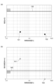
- Figs. 6(a) and 7(a) are diagrams showing the relationship between the additive amount of the conductive additive in the conductive adhesive layer and the internal resistance of the conductive adhesive layer.
- Figs. 6(b) and 7(b) are diagrams showing the relationship between the additive amount of the conductive additive in the conductive adhesive layer and the bonding strength of the conductive adhesive layer. Samples 6 to 10, which will be described below, were used in Figs. 6(a) and 7(b). Samples 11 and 12, which will be described below, were used in Figs. 7(a) and 7(b).
- Samples 6 to 10 are samples with different amounts of the first conductive assistant in the conductive adhesive layer.
- Sample 6 has the same structure and shape as Sample 1, except that the thickness of the conductive adhesive layer is 2.9 ⁇ m and the amount of the first conductive assistant is 0.1 vol.%.
- Sample 7 has the same structure and shape as Sample 6, except that the amount of the first conductive assistant is 0.2 vol.%.
- Sample 8 has the same structure and shape as Sample 6, except that the amount of the first conductive assistant is 0.4 vol.%.
- Sample 9 has the same structure and shape as Sample 6, except that the amount of the first conductive assistant is 0.8 vol.%.
- Sample 10 has the same structure and shape as Sample 6, except that the amount of the first conductive assistant is 5.0 vol.%.
- line 110 indicates the threshold resistance value.
- samples showing resistance values lower than line 110 are electrode collectors that satisfy the quality conditions for internal resistance.
- plots 111 to 115 indicate the resistance values of samples 6 to 10, respectively.
- plot 111 i.e., sample 6
- the resistance value tends to decrease as the proportion of the first conductive additive increases. For this reason, the resistance values of all of samples 7 to 10, which contain a greater amount of the first conductive additive than sample 6, are naturally lower than line 110 (see plots 112 to 115).
- the amount of the first conductive assistant when the amount of the first conductive assistant is more than 0.4 vol.%, the fluctuation in the internal resistance of the conductive adhesive layer is significantly smaller than when the amount of the first conductive assistant is 0.4 vol.% or less.
- the amount of the first conductive assistant in the conductive adhesive layer is less than 0.1 vol.%, the resistance value of the conductive adhesive layer tends to increase rapidly.
- the resistance value of the sample when the amount of the first conductive assistant in the conductive adhesive layer is 0.05 vol.% was near line 110 (not shown). Therefore, when the amount of the first conductive assistant in the conductive adhesive layer is less than 0.1 vol.%, the resistance value of the collector cannot be sufficiently reduced.
- line 120 indicates the threshold value of the bonding strength between the conductive adhesive layer and the current collecting foil contained in the sample.
- a sample showing a bonding strength higher than line 120 is a bipolar electrode current collector that satisfies the good product condition regarding the bonding strength.
- plots 121 to 125 indicate the bonding strength of the sixth to tenth samples, respectively.
- Graph 126 indicates the change in bonding strength with the change in the addition ratio of the first conductive additive.
- Graph 126 is a graph estimated based on plots 121 to 125. As shown in FIG. 6B, all of plots 121 to 124 are higher than line 120, but plot 125 is lower than line 120. Therefore, when an excessive amount of the first conductive additive is contained in the conductive adhesive layer, it can be said that a bipolar electrode current collector that does not satisfy the good product condition regarding the bonding strength is manufactured.
- Sample 11 and Sample 12 are samples with different amounts of conductive assistant in the conductive adhesive layer, and have the same shape as Sample 6.
- the amount of conductive assistant added in Sample 11 is 0.4 volume %, and the amount of conductive assistant added in Sample 12 is 5.0 volume %.
- the conductive assistant (hereinafter referred to as the second conductive assistant) contained in Sample 11 and Sample 12 is different from the first conductive assistant contained in Samples 6 to 10.
- Figure 8 shows the particle size distribution of the second conductive assistant contained in Sample 11 and Sample 12. In Figure 8, the horizontal axis shows the particle size, and the vertical axis shows the probability of existence.
- the average particle size (D50) of the second conductive assistant contained in Sample 11 and Sample 12 and shown in Figure 8 is 2.6 ⁇ m, the D10 of the second conductive assistant is 1.1 ⁇ m, and the D90 of the second conductive assistant is 5.5 ⁇ m.
- the standard deviation of the second conductive assistant is 1.2 ⁇ m.
- line 130 indicates the threshold resistance value.
- samples that show a resistance value lower than line 130 are electrode current collectors that satisfy the quality conditions for internal resistance.
- the threshold value shown by line 130 is the same as the threshold value shown by line 110 shown in FIG. 6A.
- plots 131 and 132 indicate the resistance values of the 11th and 12th samples, respectively.
- plot 131 i.e., the 11th sample
- the resistance value tends to decrease as the addition ratio of the second conductive additive increases. Therefore, the resistance value of plot 132 is naturally lower than line 110 (see plot 132).
- line 140 indicates the threshold value of the bonding strength between the conductive adhesive layer and the current collecting foil contained in the sample.
- the threshold value indicated by line 140 is the same as the threshold value indicated by line 120 shown in FIG. 6B.
- plots 141 and 142 indicate the bonding strength of the 11th and 12th samples, respectively. As shown in FIG. 7B, plot 141 is higher than line 140, but plot 142 is lower than line 140. From this data, it can be said that when the conductive adhesive layer contains an excessive amount of the second conductive additive, a bipolar electrode current collector that does not satisfy the quality conditions for bonding strength is also manufactured.
- the conductive assistant additive ratio in the conductive adhesive layer is 2.0% or less, there is a high possibility that a bipolar electrode collector that satisfies the good product conditions regarding bonding strength can be manufactured, if the additive ratio is 1.0% or less, it can be said that it is possible to reliably manufacture a bipolar electrode collector that satisfies the good product conditions regarding bonding strength, and if the additive ratio is 0.8% or less, it can be said that it is even more possible to reliably manufacture a bipolar electrode collector that satisfies the good product conditions regarding bonding strength.
- the average particle size of the conductive additive 50 may be larger than the thickness TH of the conductive adhesive layer 22. In this case, the electrical continuity between the first current collecting foil 21A and the second current collecting foil 21B via the conductive additive 50 is improved.
- each of the first current collecting foil 21A and the second current collecting foil 21B has a rectangular shape
- the length of one side of the first current collecting foil 21A and the length of one side of the second current collecting foil 21B are each 500 mm or more
- the CV value of the particle size DA of the conductive assistant 50 in the conductive adhesive layer 22 may be 10% or less.
- the conductive assistant 50 having a particle size significantly larger than the thickness TH of the conductive adhesive layer 22 is unlikely to be present in the conductive adhesive layer 22.
- the air present around the conductive assistant 50 is unlikely to be taken into the conductive adhesive layer 22 when the first current collecting foil 21A and the second current collecting foil 21B are bonded together, that is, so-called air entrapment is unlikely to occur. Therefore, an increase in the resistance of the bipolar electrode 14 due to deformation of the first current collecting foil 21A and/or the second current collecting foil 21B caused by the air is unlikely to occur.
- the first current collecting foil 21A and the second current collecting foil 21B can be well bonded to the conductive adhesive layer 22.
- the CV value of the particle size of the first conductive assistant is about 4% (0.13/3 ⁇ 100), which is smaller than 10%.
- the CV value of the particle size of the second conductive assistant is about 46% (1.2/2.6 ⁇ 100), which is significantly larger than 10%.
- each of the first current collecting foil 21A and the second current collecting foil 21B has a rectangular shape, and the length of one side of the first current collecting foil 21A and the length of one side of the second current collecting foil 21B are each 500 mm or more, and the second value obtained by adding the average particle size of the conductive assistant 50 and the standard deviation multiplied by three may be equal to or less than the thickness TH of the conductive adhesive layer 22 multiplied by two. In this case, too, the conductive assistant 50 having a particle size significantly larger than the thickness TH of the conductive adhesive layer 22 is unlikely to be present in the conductive adhesive layer 22.
- the bipolar electrode 14 is enlarged, air is unlikely to be trapped between the first current collecting foil 21A and the second current collecting foil 21B due to the conductive assistant 50. Therefore, an increase in the resistance of the bipolar electrode 14 due to deformation of the first current collecting foil 21A and/or the second current collecting foil 21B caused by the air is unlikely to occur.
- the first current collecting foil 21A and the second current collecting foil 21B can be well bonded to the conductive adhesive layer 22.
- the second value (3.39 ⁇ m) obtained by tripling the average particle size (3 ⁇ m) of the first conductive assistant and the standard deviation (0.13 ⁇ m) of the particle size of the first conductive assistant is smaller than the value (5.8 ⁇ m) obtained by doubling the thickness (2.9 ⁇ m) of the conductive adhesive layer.
- the second value (6.2 ⁇ m) obtained by tripling the average particle size (2.6 ⁇ m) of the second conductive assistant and the standard deviation (1.2 ⁇ m) of the particle size of the second conductive assistant is larger than the value (5.8 ⁇ m) obtained by doubling the thickness (2.9 ⁇ m) of the conductive adhesive layer.
- the thickness of the first current collecting foil 21A is at least twice the thickness of the second current collecting foil 21B, the thickness of the second current collecting foil 21B is less than 10 ⁇ m, the thickness TH of the conductive adhesive layer 22 is smaller than the thickness of the second current collecting foil 21B, and the CV value of the particle size DA of the conductive assistant 50 in the conductive adhesive layer 22 may be 10% or less.
- the conductive assistant 50 having a particle size significantly larger than the thickness TH of the conductive adhesive layer 22 is unlikely to exist in the conductive adhesive layer 22. This makes it difficult for air to be trapped between the first current collecting foil 21A and the second current collecting foil 21B due to the conductive assistant 50.
- the resistance of the bipolar electrode 14 is unlikely to increase due to deformation of the current collecting foil (especially the second current collecting foil 21B) due to the air.
- the resistance of the bipolar electrode 14 is unlikely to increase due to deformation of the current collecting foil (especially the second current collecting foil 21B) due to the air.
- the conductive adhesive layer 22 may further include an epoxy-based curing agent as a curing agent together with the olefin-based adhesive as the adhesive.
- the adhesive can exhibit high electrolyte resistance performance, and therefore good bonding strength can be exhibited for a long period of time.
- an epoxy-based curing agent as a curing agent when an olefin-based adhesive is used as the adhesive, gas generation in the curing reaction between the adhesive and the curing agent that occurs during the manufacture of the current collector 21 can be effectively reduced.
- isocyanate-based curing agents are also generally used as curing agents for olefin-based adhesives, and gas is generated in the curing reaction between the olefin-based adhesive and the isocyanate-based curing agent.
- the conductive adhesive layer 22 may include an epoxy-based curing agent as a curing agent together with the olefin-based adhesive as the adhesive.
- An electricity storage device including a plurality of bipolar electrodes overlapping each other in a stacking direction, Each of the plurality of bipolar electrodes includes: a first current collecting foil and a second current collecting foil overlapping each other in the stacking direction; a conductive adhesive layer located between the first current collecting foil and the second current collecting foil and bonded to the first current collecting foil and the second current collecting foil; a first active material layer located on a surface of the first current collector foil; a second active material layer located on a surface of the second current collector foil; Equipped with The conductive adhesive layer includes an adhesive and a conductive assistant dispersed in the adhesive, the conductive assistant is a spherical particle having a spherical core and a conductive film covering the core, The conductive adhesive layer contains the conductive assistant in an amount of 0.1% by volume or more and 1.0% by
- a first value obtained by adding two times the standard deviation of the particle diameter of the conductive assistant to the average particle diameter of the conductive assistant is equal to or greater than a thickness of the conductive adhesive layer;
- Energy storage device [2] The energy storage device according to [1], wherein an average particle size of the conductive assistant is greater than a thickness of the conductive adhesive layer.
- Each of the first current collecting foil and the second current collecting foil has a rectangular shape, each of a side length of the first current collecting foil and a side length of the second current collecting foil is 500 mm or more;
- the power storage device according to [1] or [2], wherein a CV value of the particle size of the conductive assistant in the conductive adhesive layer is 10% or less.
- Each of the first current collecting foil and the second current collecting foil has a rectangular shape, each of a side length of the first current collecting foil and a side length of the second current collecting foil is 500 mm or more;
- the second value obtained by adding the average particle size of the conductive assistant to three times the standard deviation is equal to or less than twice the thickness of the conductive adhesive layer.
- the thickness of the first current collecting foil is at least twice the thickness of the second current collecting foil, The thickness of the second current collecting foil is less than 10 ⁇ m, the thickness of the conductive adhesive layer is smaller than the thickness of the second current collector foil,
- the power storage device according to any one of [1] to [4], wherein a CV value of the particle size of the conductive assistant in the conductive adhesive layer is 10% or less.
- one aspect of the present disclosure is not limited to the above embodiment and the above [1] to [6].
- One aspect of the present disclosure can be further modified without departing from the spirit of the present disclosure.
- 1...electricity storage device 2...electrode laminate, 3...sealing body, 3a...outer surface, 14...bipolar electrode, 21...current collector, 21A...first current collector foil, 21B...second current collector foil, 21a...first surface, 21b...second surface, 22...conductive adhesive layer, 23...positive electrode active material layer (first active material layer), 24...negative electrode active material layer (second active material layer), 31...spacer, 31a...outer edge, 31b...inner edge, 32...sealing member, 32a...outer edge, 32b...inner edge, 40...adhesive, 50...conductive additive, 51...core, 52...conductive film, D...stacking direction, DA...particle size, T1...sealing member thickness, T2...spacer thickness, TH...conductive adhesive layer thickness.
Landscapes
- Engineering & Computer Science (AREA)
- Power Engineering (AREA)
- Chemical & Material Sciences (AREA)
- Microelectronics & Electronic Packaging (AREA)
- Materials Engineering (AREA)
- Chemical Kinetics & Catalysis (AREA)
- Electrochemistry (AREA)
- General Chemical & Material Sciences (AREA)
- Composite Materials (AREA)
- Manufacturing & Machinery (AREA)
- Cell Electrode Carriers And Collectors (AREA)
Abstract
Description
本開示は、蓄電装置に関する。 This disclosure relates to an electricity storage device.
従来の蓄電装置として、例えば特許文献1に記載のバイポーラ電池がある。この従来のバイポーラ電池は、集電体の一方の面に正極活物質層が形成され他方の面に負極活物質層が形成されてなる複数のバイポーラ電極を有している。これらのバイポーラ電極がゲル電解質層を挟んで積層されることでバイポーラ電池が構成されている。
An example of a conventional power storage device is the bipolar battery described in
上述したバイポーラ電池に用いられるバイポーラ電極用の集電体として、互いに異なる材料の金属箔を導電性接着剤を介して貼り合わせた構造(貼り合わせ箔)が利用される場合がある。上記導電性接着剤は、例えば、接着剤の主成分である熱硬化性樹脂に導電性フィラーなどの粒子状の導電助剤(導電粒子)が分散したものである。導電助剤としては、例えばカーボンブラックが広く知られている。ここで、導電助剤としてカーボンブラックを用いた導電性接着剤が貼り合わせ箔の接着に利用される場合、当該貼り合わせ箔の抵抗値を十分に小さくするためには、導電性接着剤にカーボンブラックを多量に含ませる必要がある。この場合、貼り合わせ箔の接着強度が低下してしまう問題が発生する。 As a current collector for the bipolar electrode used in the bipolar battery described above, a structure (laminated foil) in which metal foils of different materials are laminated together via a conductive adhesive may be used. The conductive adhesive may be, for example, a thermosetting resin that is the main component of the adhesive, in which a particulate conductive assistant (conductive particles) such as a conductive filler is dispersed. Carbon black is a widely known example of a conductive assistant. Here, when a conductive adhesive using carbon black as a conductive assistant is used to bond laminated foils, in order to sufficiently reduce the resistance value of the laminated foils, it is necessary to include a large amount of carbon black in the conductive adhesive. In this case, a problem occurs in that the adhesive strength of the laminated foils decreases.
本開示は、良好な接合強度と良好な導電性とを示す貼り合わせ箔を有するバイポーラ電極を備える蓄電装置を提供することを目的とする。 The present disclosure aims to provide an energy storage device equipped with a bipolar electrode having a laminated foil that exhibits good bonding strength and good electrical conductivity.
本開示の一側面に係る蓄電装置は、積層方向において互いに重なる複数のバイポーラ電極を備える蓄電装置であって、複数のバイポーラ電極のそれぞれは、積層方向において互いに重なる第1集電箔及び第2集電箔と、第1集電箔及び第2集電箔の間に位置すると共に、第1集電箔及び前記第2集電箔に接合する導電性接着層と、第1集電箔の表面上に位置する第1活物質層と、第2集電箔の表面上に位置する第2活物質層と、を備え、導電性接着層は、接着剤と、接着剤中に分散される導電助剤を含み、導電助剤は、球状のコアと、コアを被覆する導電膜とを有する球状粒子であり、導電性接着層における導電助剤の添加割合は、0.1体積%以上1.0体積%以下であり、導電助剤の平均粒径に導電助剤の粒径の標準偏差の2倍を加えた第1値は、導電性接着層の厚さ以上である。 The energy storage device according to one aspect of the present disclosure is an energy storage device including a plurality of bipolar electrodes overlapping each other in the stacking direction, each of the plurality of bipolar electrodes including a first current collecting foil and a second current collecting foil overlapping each other in the stacking direction, a conductive adhesive layer located between the first current collecting foil and the second current collecting foil and bonded to the first current collecting foil and the second current collecting foil, a first active material layer located on the surface of the first current collecting foil, and a second active material layer located on the surface of the second current collecting foil, the conductive adhesive layer includes an adhesive and a conductive assistant dispersed in the adhesive, the conductive assistant is a spherical particle having a spherical core and a conductive film covering the core, the conductive assistant is added at a rate of 0.1% by volume or more and 1.0% by volume or less, and a first value obtained by adding twice the standard deviation of the particle size of the conductive assistant to the average particle size of the conductive assistant is equal to or more than the thickness of the conductive adhesive layer.
この蓄電装置では、複数のバイポーラ電極のそれぞれは、第1集電箔と第2集電箔とを導電性接着層を介して互いに貼り合わせた貼り合わせ箔を有する。また、導電性接着層において接着剤中に分散される導電助剤は、球状のコアと、コアを被覆する導電膜とを有する球状粒子であり、導電性接着層における導電助剤の添加割合は、0.1体積%以上1.0体積%以下であり、かつ、導電助剤の平均粒径に導電助剤の粒径の標準偏差の2倍を加えた第1値は、導電性接着層の厚さ以上である。これにより、導電性接着層による第1集電箔と第2集電箔との接合強度を確保しつつ、導電性接着層の内部抵抗を十分に下げることができる。したがって、上記蓄電装置によれば、良好な接合強度と導電性とを示すバイポーラ電極を備えることができる。 In this power storage device, each of the bipolar electrodes has a laminated foil in which a first current collecting foil and a second current collecting foil are bonded to each other via a conductive adhesive layer. The conductive assistant dispersed in the adhesive in the conductive adhesive layer is a spherical particle having a spherical core and a conductive film covering the core, the conductive assistant is added at a rate of 0.1% by volume to 1.0% by volume, and a first value obtained by adding twice the standard deviation of the particle size of the conductive assistant to the average particle size of the conductive assistant is equal to or greater than the thickness of the conductive adhesive layer. This makes it possible to sufficiently reduce the internal resistance of the conductive adhesive layer while ensuring the bonding strength between the first current collecting foil and the second current collecting foil by the conductive adhesive layer. Therefore, the above-mentioned power storage device can be provided with a bipolar electrode that exhibits good bonding strength and conductivity.
導電助剤の平均粒径は、導電性接着層の厚さより大きくてもよい。この場合、導電助剤を介した第1集電箔と第2集電箔との導通がより良好になされる。 The average particle size of the conductive additive may be larger than the thickness of the conductive adhesive layer. In this case, better electrical conduction between the first current collecting foil and the second current collecting foil is achieved via the conductive additive.
第1集電箔及び第2集電箔のそれぞれは、矩形状を有し、第1集電箔の一辺の長さと、第2集電箔の一辺の長さとのそれぞれは、500mm以上であり、導電性接着層における導電助剤の粒径のCV値は、10%以下でもよい。この場合、導電性接着層の厚さに対して顕著に大きい粒径を有する導電助剤が、導電性接着層に存在しにくい。これにより、バイポーラ電極が大型化する場合であっても、第1集電箔と第2集電箔との間には、導電助剤に起因した空気の噛み込みが発生しにくくなる。よって、当該空気に起因した第1集電箔及び/または第2集電箔の変形などに伴うバイポーラ電極の抵抗増加が発生しにくくなる。加えて、バイポーラ電極が大型化する場合であっても、第1集電箔と第2集電箔とのそれぞれが導電性接着層に良好に接合可能である。 The first current collecting foil and the second current collecting foil each have a rectangular shape, the length of one side of the first current collecting foil and the length of one side of the second current collecting foil each are 500 mm or more, and the CV value of the particle size of the conductive assistant in the conductive adhesive layer may be 10% or less. In this case, the conductive assistant having a particle size significantly larger than the thickness of the conductive adhesive layer is unlikely to be present in the conductive adhesive layer. As a result, even if the bipolar electrode is enlarged, air is unlikely to be trapped between the first current collecting foil and the second current collecting foil due to the conductive assistant. Therefore, the resistance of the bipolar electrode is unlikely to increase due to deformation of the first current collecting foil and/or the second current collecting foil due to the air. In addition, even if the bipolar electrode is enlarged, each of the first current collecting foil and the second current collecting foil can be well bonded to the conductive adhesive layer.
第1集電箔及び第2集電箔のそれぞれは、矩形状を有し、第1集電箔の一辺の長さと、第2集電箔の一辺の長さとのそれぞれは、500mm以上であり、導電助剤の平均粒径に標準偏差を3倍した値を加えた第2値は、導電性接着層の厚さを2倍した値以下でもよい。この場合、導電性接着層の厚さに対して顕著に大きい粒径を有する導電助剤が、導電性接着層に存在しにくい。これにより、バイポーラ電極が大型化する場合であっても、第1集電箔と第2集電箔との間には、導電助剤に起因した空気の噛み込みが発生しにくくなる。よって、当該空気に起因した第1集電箔及び/または第2集電箔の変形などに伴うバイポーラ電極の抵抗増加が発生しにくくなる。加えて、バイポーラ電極が大型化する場合であっても、第1集電箔と第2集電箔とのそれぞれが導電性接着層に良好に接合可能である。 The first current collecting foil and the second current collecting foil each have a rectangular shape, and the length of one side of the first current collecting foil and the length of one side of the second current collecting foil are each 500 mm or more, and the second value obtained by adding the average particle size of the conductive assistant to three times the standard deviation may be equal to or less than twice the thickness of the conductive adhesive layer. In this case, a conductive assistant having a particle size significantly larger than the thickness of the conductive adhesive layer is unlikely to be present in the conductive adhesive layer. As a result, even if the bipolar electrode is enlarged, air is unlikely to be trapped between the first current collecting foil and the second current collecting foil due to the conductive assistant. Therefore, an increase in the resistance of the bipolar electrode due to deformation of the first current collecting foil and/or the second current collecting foil caused by the air is unlikely to occur. In addition, even if the bipolar electrode is enlarged, each of the first current collecting foil and the second current collecting foil can be well bonded to the conductive adhesive layer.
第1集電箔の厚さは、第2集電箔の厚さの2倍以上であり、第2集電箔の厚さは10μm未満であり、導電性接着層の厚さは、第2集電箔の厚さより小さく、導電性接着層における導電助剤の粒径のCV値は、10%以下でもよい。この場合、導電性接着層の厚さに対して顕著に大きい粒径を有する導電助剤が、導電性接着層に存在しにくい。これにより、第1集電箔と第2集電箔との間には、導電助剤に起因した空気の噛み込みが発生しにくくなる。よって、当該空気に起因した集電箔(特に第2集電箔)の変形などに伴うバイポーラ電極の抵抗増加が発生しにくくなる。 The thickness of the first current collecting foil is at least twice the thickness of the second current collecting foil, the thickness of the second current collecting foil is less than 10 μm, the thickness of the conductive adhesive layer is less than the thickness of the second current collecting foil, and the CV value of the particle size of the conductive additive in the conductive adhesive layer may be 10% or less. In this case, conductive additives having particle sizes significantly larger than the thickness of the conductive adhesive layer are unlikely to be present in the conductive adhesive layer. This makes it difficult for air to be trapped between the first current collecting foil and the second current collecting foil due to the conductive additive. This makes it difficult for the resistance of the bipolar electrode to increase due to deformation of the current collecting foil (especially the second current collecting foil) due to the air.
導電性接着層は、接着剤であるオレフィン系接着剤と共に、硬化剤であるエポキシ系硬化剤をさらに含んでもよい。この場合、接着剤として高い耐電解液性能を発揮できるので、長期間において良好な接合強度を発揮できる。加えて、接着剤としてオレフィン系接着剤が用いられるときに硬化剤としてエポキシ系硬化剤が用いられることによって、集電体の製造時にともなう接着剤と硬化剤との硬化反応におけるガス発生を良好に低減できる。 The conductive adhesive layer may further contain an epoxy-based hardener as a hardener, in addition to the olefin-based adhesive as an adhesive. In this case, the adhesive can exhibit high electrolyte resistance, and therefore good bonding strength can be exhibited over a long period of time. In addition, by using an epoxy-based hardener as a hardener when an olefin-based adhesive is used as an adhesive, gas generation during the hardening reaction between the adhesive and hardener that occurs during the production of the current collector can be effectively reduced.
本開示によれば、複数の金属箔を導電性接着剤を介して貼り合わせた貼り合わせ箔を有し、良好な接合強度と良好な導電性とを示すバイポーラ電極用集電体を備える蓄電装置を提供できる。 According to the present disclosure, it is possible to provide an electricity storage device that has a laminated foil in which multiple metal foils are bonded together via a conductive adhesive, and that is equipped with a bipolar electrode current collector that exhibits good bonding strength and good electrical conductivity.
以下、図面を参照しながら、本開示の一側面に係る蓄電装置の好適な実施形態について詳細に説明する。 Below, a preferred embodiment of an energy storage device according to one aspect of the present disclosure will be described in detail with reference to the drawings.
図1は、一実施形態に係る蓄電装置を示す模式的な断面図である。図2は、図1の要部拡大図である。図1に示す蓄電装置1は、例えばフォークリフト、ハイブリッド自動車、電気自動車等の各種車両のバッテリに用いられる装置(車両用蓄電電池)である。蓄電装置1は、例えばニッケル水素二次電池、リチウムイオン二次電池等の二次電池である。蓄電装置1は、電気二重層キャパシタであってもよく、全固体電池であってもよい。以下では、蓄電装置1がリチウムイオン二次電池である場合を例示する。
FIG. 1 is a schematic cross-sectional view showing an energy storage device according to one embodiment. FIG. 2 is an enlarged view of a main portion of FIG. 1. The
蓄電装置1は、複数のバイポーラ電極14の積層体である電極積層体2と、電極積層体2においてバイポーラ電極14の積層方向Dに延びる側面2aを封止する封止体3と、を備える。このため、蓄電装置1は、車両用バイポーラ電池とも呼称される。図1に示すように、電極積層体2は、複数のセル4を備えている。各セル4は、正極11と、負極12と、セパレータ13とを有している。
The
正極11及び負極12は、積層方向Dから見た場合に、例えば矩形状をなしている。正極11と負極12とは、セパレータ13を挟んで互いに対向して配置されている。正極11と負極12との対向方向は、バイポーラ電極14の積層方向Dと一致している。正極11は、集電体21と、集電体21の第1面21a上に設けられた正極活物質層23とによって構成されている。負極12は、集電体21と、集電体21の第2面21b上に設けられた負極活物質層24とによって構成されている。
The
図3の(a)は、集電体の要部拡大断面図である。集電体21は、リチウムイオン二次電池の放電又は充電の間、正極活物質層23及び負極活物質層24に電流を流し続けるための化学的に不活性な電気伝導体であり、バイポーラ電極14に利用される部材(バイポーラ電極用集電体)である。図3の(a)に示されるように、集電体21は、第1集電箔21A、第2集電箔21B、及び、第1集電箔21Aと第2集電箔21Bとの間に位置すると共に、第1集電箔21Aと第2集電箔21Bとを接合する導電性接着層22を有する3層構造を有する。
(a) of FIG. 3 is an enlarged cross-sectional view of a main part of the current collector. The
第1集電箔21Aと第2集電箔21Bとのそれぞれは、積層方向Dから見た場合に、例えば矩形状をなしている導電部材である。第1集電箔21Aと第2集電箔21Bとは、導電性接着層22を介して互いに一体化している。積層方向Dに沿って互いに重なる第1集電箔21Aと第2集電箔21Bとは、導電性接着層22を介して互いに電気的に接続される。第1集電箔21Aの第1面21Aaは、導電性接着層22が接するその面の反対側に位置する露出面(表面)であって、集電体21の第1面21aに相当する面である。第1集電箔21Aの第2面21Abは、導電性接着層22に接合する面である。第2集電箔21Bの第1面21Baは、導電性接着層22が接するその面の反対側に位置する露出面(表面)であって、集電体21の第2面21bに相当する面である。第2集電箔21Bの第2面21Bbは、導電性接着層22に接合する面である。積層方向Dから見て、第1集電箔21Aの一辺の長さと、第2集電箔21Bの一辺の長さとのそれぞれは、500mm以上である。当該長さは、750mm以上でもよいし、1000mm以上でもよいし、1200mm以上でもよい。
Each of the first current collecting
電極積層体2に含まれる各セル4の一部において、正極11は所定のバイポーラ電極14の一部から構成され、負極12は別のバイポーラ電極14の一部から構成される。電極積層体2では、バイポーラ電極14とセパレータ13とが交互に積層されることによって、複数のセル4が形成される。よって、複数のセル4が電気的に直列に接続されている。なお、積層方向Dにおいて隣り合うセル4,4では、同一のバイポーラ電極14が共有され得る。積層方向Dにおける電極積層体2の一端には、第1集電箔21Aを含む終端電極(正極終端電極)が配置されている。積層方向Dにおける電極積層体2の他端には、第2集電箔21Bを含む終端電極(負極終端電極)が配置されている。
In a portion of each
第1集電箔21A及び第2集電箔21Bは、例えば板状、箔状、シート状、フィルム状等の形態に形成されていてもよい。第1集電箔21A及び第2集電箔21Bを金属箔とする場合、例えばアルミニウム箔、銅箔、ニッケル箔、チタン箔又はステンレス鋼箔などが用いられる。正極電位に対する耐久性などの観点から、第1集電箔21Aは、例えば、アルミニウム箔である。負極電位に対する耐久性などの観点から、第2集電箔21Bは、例えば、銅箔である。第1集電箔21A及び第2集電箔21Bは、上記金属の合金箔、クラッド箔であってもよい。第1集電箔21A及び第2集電箔21Bが箔状の場合、積層方向Dに沿った第1集電箔21A及び第2集電箔21Bの厚さは、それぞれ、1μm以上150μm以下の範囲内であってもよい。集電体21の耐久性の観点から、第1集電箔21Aの厚さと、第2集電箔21Bの厚さとの少なくとも一方は、50μm以上であってもよいし、40μm以上であってもよいし、30μm以上であってもよい。第1集電箔21Aと第2集電箔21Bのうち、一方の厚さは、例えば、1μm以上10μm未満であり、他方の厚さは、例えば、20μm以上150μm以下である。すなわち、第1集電箔21Aと第2集電箔21Bの一方は、その厚みが10μm未満となる薄い集電箔であり、第1集電箔21Aと第2集電箔21Bの他方は、上記薄い集電箔の2倍以上の厚みを有する集電箔である。
The first current collecting
本実施形態では、第1集電箔21Aはアルミニウム箔であり、第2集電箔21Bは銅箔である。第1集電箔21Aであるアルミニウム箔及び第2集電箔21Bである銅箔は、導電性接着層22を介した貼り合わせにより一体化されている。このため、集電体21は、第1集電箔21Aと第2集電箔21Bとを導電性接着層22を介して互いに貼り合わせた箔(貼り合わせ箔)と言える。コスト、重量などの観点から、集電体21において、第1集電箔21Aの厚さは、第2集電箔21Bの厚さよりも大きくなっている。バイポーラ電極14に含まれる第1集電箔21Aの厚さは、例えば、40μm以上100μm以下である。集電体21の強度の観点から、第1集電箔21Aの厚さは、第2集電箔21Bの厚さの5倍以上でもよい。この場合、例えば、第2集電箔21Bの厚さを9μm以下としても、第1集電箔21Aの厚さが45μm以上とできるので、集電体21の強度を貼り合わせ箔として十分な強度とできる。バイポーラ電極14に含まれる第2集電箔21Bの厚さは、例えば、5μm以上10μm未満である。一方、電極積層体2の最外電極を構成する正極終端電極に含まれる第1集電箔21Aの厚さは、100μm以上150μm以下であってもよい。また、電極積層体2の最外電極を構成する負極終端電極としては、集電体21と同じ貼り合わせ箔が用いられる。負極終端電極に含まれる第1集電箔の厚さは、100μm以上150μm以下であってもよい。すなわち、第1集電箔を厚く構成することによって、薄い第2集電箔を補強することができる。
In this embodiment, the first current collecting
導電性接着層22は、第1集電箔21Aと第2集電箔21Bとを接合して互いに一体化する異方性導電部材であって、積層方向Dにおいて第1集電箔21Aと第2集電箔21Bとの間に位置する。加えて、導電性接着層22は、第1集電箔21Aと第2集電箔21Bとを互いに電気的に接続させる部材である。第1集電箔21Aと第2集電箔21Bとの接合強度確保、集電体21の内部抵抗低減、集電体21の厚さ低減などの観点から、導電性接着層22の厚さTHは、例えば2μm以上5μm以下である。図3の(a)に示すように、導電性接着層22は、接着剤40と、接着剤40内に分散される複数の導電助剤50とを有する。
The conductive
接着剤40は、第1集電箔21A及び第2集電箔21Bの両方に対して接着性を示す樹脂を含む。当該樹脂としては、例えば、ポリエチレン、ポリプロピレン、ポリブチレン等のオレフィン系樹脂、エチレン-酢酸ビニル共重合体(EVA)、ポリエチレンテレフタレート(PET)、ポリエチレンナフタレート(PEN)、ポリエーテルニトリル(PEN)、ポリイミド(PI)、ポリアミド(PA)、ポリテトラフルオロエチレン(PTFE)、スチレン-ブタジエンゴム(SBR)、ポリアクリロニトリル(PAN)、ポリメチルアクリレート(PMA)、ポリメチルメタクリレート(PMMA)、ポリ塩化ビニル(PVC)、ポリフッ化ビニリデン(PVDF)、シリコーン、エポキシ樹脂、またはこれらの混合物が挙げられる。上述した樹脂のイオン伝導性が低いため、接着剤40を介したリチウムイオンの透過を抑制できる。蓄電装置1に収容される電解質に対する耐性などの観点から、上記樹脂は、オレフィン系樹脂の接着剤(ポリエチレン、ポリプロピレン等のオレフィン系接着剤)などでもよい。オレフィン系接着剤の分子量は、例えば、数万以下である。この場合、接着剤40における上記樹脂の溶剤への分散性が、良好になる。一例では、オレフィン系接着剤は、低分子ポリプロピレン(分子量が数万以下のポリプロピレン)である。接着剤40の厚さは、導電性接着層22の厚さTHに相当する。
The adhesive 40 includes a resin that exhibits adhesiveness to both the first current collecting
接着剤40には、上記樹脂に加えて、硬化剤、アンチブロッキング剤、酸化防止剤、光安定剤などの種々の添加剤が含まれてもよい。上記樹脂がオレフィン系樹脂の接着剤である場合、硬化剤としては、例えばイソシアネート系硬化剤、エポキシ系硬化剤等が用いられる。オレフィン系樹脂を接着成分とする接着剤で2枚の金属箔を接合する場合には、硬化反応に伴うガス発生防止の観点から、硬化剤としてエポキシ系硬化剤が用いられてもよい。 In addition to the resin, the adhesive 40 may contain various additives such as a hardener, an antiblocking agent, an antioxidant, and a light stabilizer. When the resin is an olefin-based resin adhesive, the hardener may be, for example, an isocyanate-based hardener or an epoxy-based hardener. When two metal foils are joined with an adhesive containing an olefin-based resin as an adhesive component, an epoxy-based hardener may be used as the hardener to prevent gas generation associated with the hardening reaction.
導電助剤50は、導電性接着層22において第1集電箔21Aと第2集電箔21Bとの導通経路となる部材であり、接着剤40内に分散している。導電助剤50としては、球状粒子が用いられる。ここで、球状の粒子は、真球状の粒子だけでなく、楕円球状の粒子を含み得る。導電助剤50は、球状のコア51と、コア51を被覆する導電膜52とを有する。コア51は、導電助剤50における本体部であり、球状を呈する部材である。コア51を形成する部材としては、例えば、シリカ等のセラミックス材料、もしくは、エポキシ樹脂、アクリル樹脂、ウレタン樹脂、ナイロン樹脂、シリコーン樹脂等の樹脂材料が用いられる。導電膜52は、導電助剤50において電気伝導性を発揮する部分であり、コア51の全体を被覆する。導電膜52は、例えば、コア51をコーティングする金属薄膜、合金薄膜などである。当該金属薄膜及び当該合金薄膜は、金、銀、銅、白金、ニッケル、パラジウム、アルミニウムなどの金属を含む。
The
複数の導電助剤50の少なくとも一部では、その粒径DAは、導電性接着層22の厚さTHよりも大きい。このため、一部の導電助剤50は、接着剤40から露出し、第1集電箔21A及び第2集電箔21Bの両方に接触し得る。この導電助剤50を介して第1集電箔21Aと第2集電箔21Bとが互いに導通する。導電助剤50の平均粒径をD50とし、導電助剤50の粒径DAの標準偏差の値をδとしたとき、導電助剤50の平均粒径に導電助剤50の粒径DAの標準偏差を2倍した値を加えた値(D50+2δ、第1値)は、導電性接着層22の厚さTHより大きい。これにより、導電性接着層22において、第1集電箔21A及び第2集電箔21Bの両方に接触する導電助剤50が多数存在し得る。よって、少量の添加量であっても集電体21の内部抵抗を十分に低減できる。なお、本実施形態では、導電助剤50の平均粒径は、接着剤40の厚さより大きい。また、本実施形態では、導電助剤50の平均粒径に導電助剤50の粒径DAの標準偏差を加えた値(D50+δ)も、導電性接着層22の厚さTHより大きい。
In at least some of the
導電助剤50の粒度分布は、例えば、コールター法、画像解析法、レーザー回折・散乱法など公知の手法で測定される。導電助剤50の粒径DAは、例えば、走査型電子顕微鏡(SEM)、透過型電子顕微鏡(TEM)などの観察手段を用いて得られる導電助剤50の輪郭線上における任意の2点間の距離のうち、最大の距離に相当する。導電助剤50の平均粒径(D50)は、測定粒子の粒径分布において、ある粒子径より大きい粒子の個数(又は質量)が、全測定粒子の個数(又は質量)の50%を占めるときの粒子径をいう。D10は、測定粒子の粒径分布において、ある粒子径より大きい粒子の個数(又は質量)が、全測定粒子の個数(又は質量)の10%を占めるときの粒子径をいう。D90は、測定粒子の粒径分布において、ある粒子径より大きい粒子の個数(又は質量)が、全測定粒子の個数(又は質量)の90%を占めるときの粒子径をいう。また、導電助剤50の平均粒径は、粉末に対するレーザー回折・散乱法で得られる体積基準の累積粒度分布における累積値が50%となったときの粒子径に相当する。上記累積値が10%となったときの粒子径がD10に相当し、上記累積値が90%となったときの粒子径がD90に相当する。ここで、導電助剤50における、式「(D50-D10)/D50」と式「(D90-D50)/D50」により算出される粒度分布のばらつきを表す値は、それぞれ、0.5以下でもよいし、0.3以下でもよいし、0.1以下でもよい。また、導電助剤50の粒径DAの標準偏差は、例えば10000個~30000個の粒子の粒子径から求められる標準偏差に相当する。
The particle size distribution of the
本実施形態では、導電助剤50の平均粒径に導電助剤50の粒径DAの標準偏差を3倍した値を加えた値(D50+3δ、第2値)は、導電性接着層22の厚さTHを2倍した値以下である。これにより、極端に大きな粒子径を有する導電助剤50が導電性接着層22に含まれない、もしくはほぼ含まれない。このため、集電体21の製造時に空気の噛み込みが発生しにくくなる(すなわち、集電体21の製造時に第1集電箔21Aと第2集電箔21Bとの間に空気が留まる領域が設けられにくくなる)。よって、上記空気に起因した集電体21の内部抵抗の増加を抑制できる(詳細は、後述する)。
In this embodiment, the value (D50+3δ, second value) obtained by adding three times the standard deviation of the particle diameter DA of the
導電性接着層22における導電助剤50の粒径DAのCV値(変動係数)は、10%以下でもよい。上記変動係数は、式:「CV値(%)=(δ/D50)×100」で表される。導電助剤50の粒径DAのCV値は、7%以下でもよいし、5%以下でもよいし、3%以下でもよい。粒径のCV値が低いことは、粒子の単分散性がよいということを意味する。ここでは、導電助剤50の粒径DAのCV値が低いほど、導電助剤50の粒子径分布が狭いことを意味する。導電助剤50の粒径DAのCV値が10%以下である場合、極端に大きな粒子径を有する導電助剤50が導電性接着層22に含まれない、もしくはほぼ含まれないと言える。このため、集電体21の製造時に空気の噛み込みが発生しにくくなる(すなわち、集電体21の製造時に第1集電箔21Aと第2集電箔21Bとの間に空気が留まる領域が設けられにくくなる)。よって、上記空気に起因した集電体21の内部抵抗の増加を抑制できる(詳細は、後述する)。
The CV value (coefficient of variation) of the particle diameter DA of the
導電性接着層22における導電助剤50の添加割合は、0.1体積%以上1.0体積%以下である。この場合、導電性接着層22を介した第1集電箔21Aと第2集電箔21Bとの接合強度を確保しつつ、集電体21の内部抵抗を低下できる。当該添加割合は、0.1体積%以上0.8体積%以下でもよいし、0.2体積%以上0.8体積%以下でもよいし、0.4体積%以上0.6体積%以下でもよいし、0.1体積%以上0.5体積%以下でもよい。
The proportion of
図1及び図2に戻って、正極活物質層23は、矩形状の第1集電箔21Aの第1面21Aaにおける平面視中央部に矩形状に設けられている部材(第1活物質層)である。負極活物質層24は、矩形状の第2集電箔21Bの第1面21Baにおける平面視中央部に矩形状に設けられている部材(第2活物質層)である。集電体21の縁部21cには、第1面21Aa側において正極活物質層23が設けられていない領域が形成され、第1面21Ba側において負極活物質層24が設けられていない領域が形成されている。負極活物質層24は、正極活物質層23よりも一回り大きく形成されている。積層方向Dから見た場合に、正極活物質層23の形成領域の全体が負極活物質層24の形成領域内に位置している。
1 and 2, the positive electrode
正極活物質層23は、リチウムイオン等の電荷担体を吸蔵及び放出し得る正極活物質を含む。正極活物質としては、例えば複合酸化物、金属リチウム、及び硫黄等が挙げられる。複合酸化物の組成には、例えば鉄、マンガン、チタン、ニッケル、コバルト、及びアルミニウムの少なくとも1つと、リチウムとが含まれる。複合酸化物としては、オリビン型リン酸鉄リチウム(LiFePO4)、コバルト酸リチウム(LiCoO2)、リチウムニッケルコバルトマンガン酸化物(LiNiMnCoO2)等が挙げられる。
The positive electrode
負極活物質層24は、リチウムイオン等の電荷担体を吸蔵及び放出し得る負極活物質を含む。負極活物質としては、例えば黒鉛、人造黒鉛、高配向性グラファイト、メソカーボンマイクロビーズ、ハードカーボン、ソフトカーボン等のカーボン、金属化合物、リチウムと合金化可能な元素もしくはその化合物、ホウ素添加炭素等が挙げられる。リチウムと合金化可能な元素の例としては、ケイ素(Si)及びスズが挙げられる。
The negative electrode
正極活物質層23及び負極活物質層24には、活物質のほか、結着剤及び導電助剤が含まれ得る。結着剤は、活物質又は導電助剤を互いに繋ぎ止め、電極中の導電ネットワークを維持する役割を果たす。結着剤としては、ポリフッ化ビニリデン、ポリテトラフルオロエチレン、フッ素ゴム等の含フッ素樹脂、ポリプロピレン、ポリエチレン等の熱可塑性樹脂、ポリイミド、ポリアミドイミド等のイミド系樹脂、アルコキシシリル基含有樹脂、ポリアクリル酸やポリメタクリル酸等のアクリル系樹脂、スチレン-ブタジエンゴム、カルボキシメチルセルロース、アルギン酸ナトリウム、アルギン酸アンモニウム等のアルギン酸塩、水溶性セルロースエステル架橋体、デンプン-アクリル酸グラフト重合体を例示することができる。これらの結着剤は、単独で又は複数で用いられ得る。導電助剤は、例えばアセチレンブラック、カーボンブラック、グラファイト等の導電性材料であり、電気伝導性を高めることができる。粘度調整溶媒には、例えばN-メチル-2-ピロリドン等が用いられる。
The positive electrode
集電体21への正極活物質層23及び負極活物質層24の形成には、例えばロールコート法、ダイコート法、ディップコート法、ドクターブレード法、スプレーコート法、カーテンコート法等の公知の方法が用いられる。具体的には、活物質、溶剤、並びに必要に応じて結着剤及び導電助剤を混合してスラリー状の活物質層形成用組成物を製造し、当該活物質層形成用組成物を集電体21に塗布後、乾燥する。溶剤には、例えばN-メチル-2-ピロリドン、メタノール、メチルイソブチルケトン、水などを用いることができる。電極密度を高めるべく、乾燥後の活物質層形成用組成物を圧縮してもよい。
The positive electrode
セパレータ13は、積層方向Dにおいて、正極11と負極12との間に配置されている。セパレータ13は、電極積層体2において隣り合う正極11と負極12とを隔離することで、両極の接触による電気的短絡を防止しつつ、リチウムイオン等の電荷担体を通過させる部材である。セパレータ13は、積層方向Dに互いに対向する正極活物質層23及び負極活物質層24の間に配置されている。
The
セパレータ13は、積層方向Dから見た場合に、正極活物質層23及び負極活物質層24よりも一回り大きく、かつ集電体21よりも一回り小さい矩形状をなしている。セパレータ13の端部13aは、積層方向Dから見た場合に、正極活物質層23及び負極活物質層24よりも外側に位置する。セパレータ13の端部13aは、後述するシール部材32に溶着されている。
When viewed from the stacking direction D, the
セパレータ13は、例えばシート状に形成されている。セパレータ13は、例えば電解質を吸収保持するポリマーを含む多孔性シート又は不織布によって構成されている。セパレータ13を構成する材料としては、例えば、ポリプロピレン、ポリエチレン、ポリオレフィン、ポリエステルなどが挙げられる。セパレータ13は、単層構造であってもよいし、多層構造であってもよい。多層構造の場合、セパレータ13は、例えば基材層及び一対の接着層を含み、一対の接着層によって正極活物質層23及び負極活物質層24に接着固定されてもよい。セパレータ13は、耐熱層となるセラミック層を含んでいてもよい。セパレータ13は、ポリフッ化ビニリデンのようなフッ化ビニリデン樹脂化合物で補強されていてもよい。
The
セパレータ13に含浸される電解質としては、例えば非水溶媒と非水溶媒に溶解した電解質塩とを含む液体電解質(電解液)、ポリマーマトリックス中に保持された電解質を含む高分子ゲル電解質などが挙げられる。セパレータ13に電解質が含浸される場合、その電解質塩としては、LiFSI、LiClO4、LiAsF6、LiPF6、LiBF4、LiCF3SO3、LiN(FSO2)2、LiN(CF3SO2)2等の公知のリチウム塩を使用できる。非水溶媒としては、環状カーボネート類、環状エステル類、鎖状カーボネート類、鎖状エステル類、エーテル類等の公知の溶媒を使用できる。これら公知の溶媒材料を二種以上組合せて用いてもよい。
Examples of the electrolyte impregnated in the
封止体3は、電極積層体2の積層方向Dに延びる側面2aを封止する部材である。封止体3は、積層方向Dに隣り合う一対の集電体21,21が接触しないようにそれらの間隔を保持するとともに、当該一対の集電体21,21の間の空間Sを封止する。すなわち、積層方向Dに隣り合う集電体21,21と封止体3とによって空間Sが画定されている。空間Sには、正極活物質層23と負極活物質層24とセパレータ13と電解質が収容されている。
The sealing
封止体3は、複数の枠状のスペーサ31と、複数の枠状のシール部材32とによって構成されている。スペーサ31とシール部材32のそれぞれは、樹脂材料により構成されている。シール部材32は、バイポーラ電極14に含まれる集電体21の両面、正極終端電極に含まれる第1集電箔21Aの両面、及び、負極終端電極に含まれる第2集電箔21Bの両面のそれぞれにおける縁部21cに溶着されている。本実施形態では、図2に示すように、シール部材32は、集電体21の縁部21cを覆うように設けられている、すなわち、シール部材32は、集電体21の縁部21cにおいて、第1面21aと第2面21bとの双方に接し、これらを繋ぐように更に集電体21の側端面21dにも位置している。スペーサ31は、積層方向Dに隣り合う集電体21,21間であって、かつ、積層方向Dに隣り合うシール部材32,32間に配置されている。
The sealing
シール部材32は、集電体21と積層方向Dに重なる重なり部分と、集電体21の縁部21cよりも外側に張り出して集電体21と積層方向Dに重ならない張り出し部分とを備える。シール部材32は、第1面21aとの重なり部分の全体で第1面21aに溶着され、第2面21bとの重なり部分の全体で第2面21bに溶着されている。シール部材32は、張り出し部分において集電体21の側端面21dを覆っている。例えば、シール部材32は、集電体21の一方面側に配置された第1シールと集電体21の他方面側に配置された第2シールとが張り出し部分において互いに溶着されることで、集電体21の側端面21dを覆っている。
The sealing
スペーサ31は、積層方向Dに隣り合う集電体21,21の間隔を所定の間隔に保持する部材である。スペーサ31は、積層方向Dに隣り合う集電体21,21のそれぞれの縁部21cを覆うシール部材32,32間に配置されている。スペーサ31の厚さT2は、シール部材32における集電体21の一方面に溶着されている部分の厚さT1よりも大きくなっている。
The
本実施形態では、シール部材32が集電体21の縁部21cを覆うように設けられており、シール部材32において集電体21の第1面21a上に位置する部分の厚さは、シール部材32において集電体21の第2面21b上に位置する部分の厚さとは等しい。なお、本実施形態では、図2に示すように、シール部材32の厚さT1は、シール部材32において集電体21の第2面21b上に位置する部分の厚さで規定する。スペーサ31の厚さT2は、積層方向Dに隣り合うシール部材32,32間に位置する部分の厚さで規定する。シール部材32の厚さT1に対するスペーサ31の厚さT2の比は、例えば1:2~1:4となっている。
In this embodiment, the sealing
シール部材32の外縁部32a及びスペーサ31の外縁部31aは、いずれも、積層方向Dから見て、集電体21の縁部21cよりも外側に張り出している。各スペーサ31において集電体21の縁部21cよりも外側に張り出す外縁部31aと、当該スペーサ31に積層方向Dに隣り合うシール部材32において集電体21の縁部21cよりも外側に張り出す外縁部32aとは、それぞれの端面側で互いに溶着されることによって溶着部Wを形成している。この溶着部Wによって封止体3の外表面3aが形成されている。スペーサ31の外縁部31aとシール部材32の外縁部32aとの溶着には、例えば赤外線溶着、熱板溶着などの手法を用いることができる。溶着部Wでは、シール部材32を構成する樹脂材料とスペーサ31を構成する樹脂材料との相溶により、積層方向Dに隣り合う集電体21,21の間の空間Sのシール性が担保されている。
The
溶着部Wの内側では、スペーサ31は、積層方向Dに隣り合う一方の集電体21に接するシール部材32及び他方の集電体21に接するシール部材32のいずれに対しても非溶着となっている。非溶着部分では、スペーサ31と、一方の集電体21に接するシール部材32とは、接触していてもよく、僅かに離間していてもよい。同様に、非溶着部分では、スペーサ31と、他方の集電体21に接するシール部材32とは、接触していてもよく、僅かに離間していてもよい。スペーサ31は、積層方向Dに隣り合う集電体21,21のいずれに対しても非溶着となっている。
Inside the welded portion W, the
集電体21の第1面21a上において、シール部材32の内縁部32bには、上述したセパレータ13の端部13aが溶着されている。本実施形態では、シール部材32の内縁部32bは、スペーサ31の内縁部31bと揃っているが、これに限られない。シール部材32の内縁は、スペーサ31の内縁部とずれていてもよい。シール部材32の内縁部32bが、スペーサ31の内縁部31bよりも集電体21の内側に張り出してもよいし、内縁部31bが、内縁部32bよりも集電体21の内側に張り出してもよい。
On the
シール部材32及びスペーサ31を構成する樹脂材料としては、例えば酸変性ポリエチレン(酸変性PE)、酸変性ポリプロピレン(酸変性PP)、ポリエチレン、ポリプロピレン等の耐電解質性を有する材料が挙げられる。シール部材32を構成する樹脂材料とスペーサ31を構成する樹脂材料とは、同じであってもよく、異なっていてもよい。
The resin material constituting the sealing
本実施形態では、シール部材32を構成する樹脂材料は、酸変性ポリエチレン又は酸変性ポリプロピレンとなっており、スペーサ31を構成する樹脂材料は、ポリエチレン又はポリプロピレンとなっている。酸変性ポリエチレン及び酸変性ポリプロピレンは、酸変性されていないポリエチレン及び酸変性されていないポリプロピレンと比較して、金属に接着し易い性質を有している。集電体21が銅箔やアルミ箔といった金属箔からなる本実施形態では、シール部材32を酸変性ポリエチレン又は酸変性ポリプロピレンによって構成することで、集電体21に対するシール部材32の接着強度(接合強度)を向上させることができる。集電体21との接着が要求されないスペーサ31では、安価なポリエチレン又はポリプロピレンを用いることで、蓄電装置1の低コスト化が図られる。
In this embodiment, the resin material constituting the sealing
次に、図4を参照しながら本実施形態に係る集電体21の製造方法の一例について説明する。図4は、集電体の製造に利用される塗工装置を示す模式図である。
Next, an example of a method for manufacturing the
図4に示す塗工装置60は、集電体21を製造するための装置であり、送り出しロール61,62と、一対のグラビアロール63a,63bと、乾燥炉64と、一対の受けロール65a,65bと、巻き取りロール66と、液体Lを収容する容器67とを有する。液体Lは、導電性接着層22の材料である接着剤、導電助剤などが分散している溶剤である。
The
送り出しロール61は、後に第1集電箔21Aとなる金属箔MB1が巻回される。送り出しロール62は、後に第2集電箔21Bとなる金属箔MB2が巻回される。金属箔MB1は、送り出しロール61より一対のグラビアロール63a,63bに向かって送り出される。金属箔MB2は、送り出しロール62より一対の受けロール65a,65bに向かって送り出される。
The metal foil MB1, which will later become the first
グラビアロール63a,63bは、送り出しロール61の下流に位置し、金属箔MB1に液体Lを塗布する。グラビアロール63aの一部は、容器67に収容される液体Lに接している。これにより、グラビアロール63aの回転に伴って、グラビアロール63aに液体Lが付着し、当該液体Lが金属箔MB1に転写される。
The gravure rolls 63a and 63b are located downstream of the
乾燥炉64は、グラビアロール63a,63bの下流に位置し、金属箔MB1に付着する液体Lの溶媒を除去する部材である。乾燥炉64を通過した金属箔MB1には、導電性接着層22(図2などを参照)が設けられる。
The drying
受けロール65a,65bは、乾燥炉64及び送り出しロール62の下流に位置し、導電性接着層22が設けられる金属箔MB1と、送り出しロール62から送り出される金属箔MB2とを受け取る。受けロール65a,65bの間にて、金属箔MB1,MB2が、導電性接着層22を介して互いに押圧される。これにより、導電性接着層22を介して金属箔MB1,MB2が互いに貼り合わされる。よって、受けロール65a,65bから、後に集電体21となる貼り合わせ箔LBが送り出される。
The receiving rolls 65a, 65b are located downstream of the drying
巻き取りロール66は、受けロール65a,65bの下流に位置し、貼り合わせ箔LBを巻き取る。巻き取られた貼り合わせ箔LBは、バイポーラ電極14を製造するための製造装置に移載される。当該製造装置では、貼り合わせ箔LBに対して正極活物質層23及び負極活物質層24を形成した後、貼り合わせ箔LBが所定の形状に切断される。これにより、正極11及び負極12を有するバイポーラ電極14が製造される。ここで、正極活物質層23の製造においては、後に正極活物質層23となるスラリーを貼り合わせ箔LBに塗布した後、当該スラリーを乾燥する乾燥工程が実施される。同様に、負極活物質層24の製造においても、上記乾燥工程と同様の乾燥工程が実施される。これらの乾燥工程では、例えば150℃程度に設定された乾燥炉に上記スラリー及び貼り合わせ箔LBが収容される。よって、貼り合わせ箔LBも150℃程度まで加熱される。貼り合わせ箔LBの製造時に多量の空気が噛み込まれている場合、上記加熱により、導電性接着層22内において当該空気が膨張する。これにより、金属箔MB1と金属箔MB2との間の距離が広がってしまったり、接触していた導電助剤と金属箔MB1または金属箔MB2との間に浮きが発生してしまったりするおそれがある。導電性接着層22にこのような膨張空気による空間が形成されると、導電性接着層22を介した金属箔MB1と金属箔MB2との導通が阻害され、結果的に貼り合わせ箔LBの内部抵抗が上昇してしまう。したがって導電性接着層22においては、接着剤40の厚さと、導電助剤50の平均粒径(D50)、上記第1値、上記第2値、導電助剤50の粒径DAのCV値などとの関係は、空気の噛み込み抑制等の観点から肝要であると言える。なお、バイポーラ電極14が大型であるほど、空気の噛み込みは発生しやすい傾向がある。バイポーラ電極14が大型化するほど、金属箔MB1,MB2の搬送方向に直交する方向において、金属箔MB1,MB2の中央部から端部までの距離が長くなる。金属箔MB1,MB2を重ねたときに上記中央部付近で金属箔MB1,MB2間に空気が取り込まれてしまうと、金属箔MB1,MB2の押圧接着時に当該空気を完全に押出し除去することは、上記距離が長くなるほど困難になるためである。この観点からも、上記関係は肝要であると言える。
The winding
以上に説明した本実施形態に係る蓄電装置1では、バイポーラ電極14は、第1集電箔21Aと第2集電箔21Bとを導電性接着層22を介して互いに貼り合わせた貼り合わせ箔である集電体21を有する。また、導電性接着層22において接着剤40中に分散される導電助剤50は、球状のコア51と、コア51を被覆する導電膜52とを有する球状粒子であり、導電性接着層22における導電助剤50の添加割合は、0.1体積%以上1.0体積%以下であり、導電助剤50の平均粒径に導電助剤50の粒径DAの標準偏差の2倍を加えた第1値は、導電性接着層22の厚さTH以上である。これにより、導電助剤50を介した第1集電箔21Aと第2集電箔21Bとの導通が良好になされるので、導電性接着層22の内部抵抗を十分に下げることができる。加えて、導電性接着層22による第1集電箔21Aと第2集電箔21Bとの接合強度を確保できる。したがって、蓄電装置1によれば、良好な接合強度と導電性とを示すバイポーラ電極14を備えることができる。
In the
ここで、図5の(a),(b)を参照しながら、上記第1値を、導電性接着層22の厚さTHより大きくすることの作用効果を詳細に説明する。図5の(a)は、導電性接着層に分散される第1導電助剤の粒度分布を示す図である。図5の(a)において、横軸は粒径を示し、縦軸は存在確率(頻度)を示す。図5の(a)には、以下に説明する第1サンプル~第5サンプルに含まれる第1導電助剤の粒度分布が示される。図5の(a)に示されるグラフ101の形状からわかるように、第1導電助剤は、その粒径が3.0μm及びその近傍である粒子が多数を占めると共に、その粒径が2.5μm未満の粒子と、その粒径が3.4μm以上の粒子をほぼ含まない。グラフ101に示される第1導電助剤の平均粒径(D50)は3μmであり、第1導電助剤のD10は2.8μmであり、第1導電助剤のD90は3.2μmである。なお、第1導電助剤の標準偏差は0.13μmである。
Here, the effect of making the first value greater than the thickness TH of the conductive
図5の(b)は、導電性接着層の厚さと、サンプルの抵抗値との関係を示す図である。図5の(b)には、以下に説明する第1集電箔、第2集電箔及び導電性接着層を有する集電体から切り取った2.5cm角のサンプルの測定結果が示される。図5の(b)において、横軸は導電性接着層の厚さ(膜厚)を示し、縦軸は第1サンプル~第5サンプルの抵抗値を示す。 Figure 5(b) is a diagram showing the relationship between the thickness of the conductive adhesive layer and the resistance value of the sample. Figure 5(b) shows the measurement results of a 2.5 cm square sample cut from a collector having a first current collecting foil, a second current collecting foil, and a conductive adhesive layer, which will be described below. In Figure 5(b), the horizontal axis shows the thickness (film thickness) of the conductive adhesive layer, and the vertical axis shows the resistance values of the first to fifth samples.
第1サンプルは、第1集電箔である厚さ50μmのアルミニウム箔と、第2集電箔である厚さ8μmの銅箔とが、以下に説明する導電性接着層によって一体化された集電体である。当該導電性接着層は、主成分であるオレフィン系樹脂及びエポキシ系硬化剤を含む接着剤と、当該接着剤に分散される第1導電助剤とを有する層状部材であり、その厚さは約2.2μmである。第1サンプルにおいて、第1導電助剤の添加量は、0.2体積%と設定した。第2サンプルは、導電性接着層の厚さが約2.6μmであること以外は上記第1サンプルと同一である。第3サンプルは、導電性接着層の厚さが約2.9μmであること以外は上記第1サンプルと同一である。第4サンプルは、導電性接着層の厚さが約3.2μmであること以外は上記第1サンプルと同一である。第5サンプルは、導電性接着層の厚さが約3.55μmであること以外は上記第1サンプルと同一である。 The first sample is a collector in which a 50 μm thick aluminum foil serving as a first current collecting foil and a 8 μm thick copper foil serving as a second current collecting foil are integrated by a conductive adhesive layer described below. The conductive adhesive layer is a layered member having an adhesive containing an olefin resin as a main component and an epoxy hardener, and a first conductive assistant dispersed in the adhesive, and has a thickness of about 2.2 μm. In the first sample, the amount of the first conductive assistant added was set to 0.2 volume %. The second sample is the same as the first sample except that the conductive adhesive layer is about 2.6 μm thick. The third sample is the same as the first sample except that the conductive adhesive layer is about 2.9 μm thick. The fourth sample is the same as the first sample except that the conductive adhesive layer is about 3.2 μm thick. The fifth sample is the same as the first sample except that the conductive adhesive layer is about 3.55 μm thick.
図5の(b)において、ライン102は抵抗値の閾値を示す。プロット103~107は、第1サンプル~第5サンプルの抵抗値をそれぞれ示す。ここでは、ライン102よりも低い抵抗値を示すサンプルは、内部抵抗に関する良品条件を満足する電極用集電体である。図5の(b)に示されるように、プロット107のみが、ライン102よりも高い抵抗値を示した。これは、導電性接着層の厚さ(約3.55μm)が、第1導電助剤の平均粒径(3μm)に第1導電助剤の粒径の標準偏差(0.13μm)の2倍を加えた第1値(3.26μm)よりも明らかに大きいため、第1導電助剤を介した第1集電箔と第2集電箔との導通が不十分であったと推察される。このため、プロット103~106に示されるように、上記第1値が導電性接着層の厚さよりも大きいことによって、第1導電助剤を介した第1集電箔と第2集電箔との導通が良好になされると推察される。
In FIG. 5B,
続いて、図6の(a),(b)及び図7の(a),(b)を参照しながら、導電性接着層22における導電助剤50の添加割合を0.1体積%以上1.0体積%以下と設定したことによる作用効果を詳細に説明する。図6の(a)及び図7の(a)のそれぞれは、導電性接着層における導電助剤の添加量と、導電性接着層の内部抵抗との関係を示す図である。図6の(b)及び図7の(b)のそれぞれは、導電性接着層における導電助剤の添加量と、導電性接着層の接合強度との関係を示す図である。図6の(a),(b)には以下に説明する第6サンプル~第10サンプルが用いられた。また、図7の(a),(b)には以下に説明する第11サンプル及び第12サンプルが用いられた。
Next, the effect of setting the additive ratio of the
第6サンプル~第10サンプルは、導電性接着層における第1導電助剤の添加量が互いに異なるサンプルである。第6サンプルは、導電性接着層の厚さが2.9μmであること、ならびに、第1導電助剤の添加量が0.1体積%であること以外は、第1サンプルと同様の構成及び形状を有する。第7サンプルは、第1導電助剤の添加量が0.2体積%であること以外は、第6サンプルと同様の構成及び形状を有する。第8サンプルは、第1導電助剤の添加量が0.4体積%であること以外は、第6サンプルと同様の構成及び形状を有する。第9サンプルは、第1導電助剤の添加量が0.8体積%であること以外は、第6サンプルと同様の構成及び形状を有する。第10サンプルは、第1導電助剤の添加量が5.0体積%であること以外は、第6サンプルと同様の構成及び形状を有する。
Samples 6 to 10 are samples with different amounts of the first conductive assistant in the conductive adhesive layer. Sample 6 has the same structure and shape as
図6の(a)において、ライン110は抵抗値の閾値を示す。ここでは、ライン110よりも低い抵抗値を示すサンプルは、内部抵抗に関する良品条件を満足する電極用集電体である。図6の(a)において、プロット111~115は、第6サンプル~第10サンプルの抵抗値をそれぞれ示す。図6の(a)に示されるように、導電性接着層における第1導電助剤の添加割合を0.1体積%とした場合であっても、プロット111(すなわち、第6サンプル)はライン110よりも低くなっている。また、第1導電助剤の添加割合が増えるほど、抵抗値が低くなる傾向がある。このため、第6サンプルよりも第1導電助剤の添加量が多い第7サンプル~第10サンプルのいずれの抵抗値も、当然にライン110よりも低くなっている(プロット112~115を参照)。ただ、第1導電助剤の添加量が0.4体積%より大きい場合、第1導電助剤の添加量が0.4体積%以下である場合よりも、導電性接着層の内部抵抗の変動が顕著に小さい。一方、導電性接着層における第1導電助剤の添加割合が0.1体積%未満である場合、導電性接着層の抵抗値が急激に高くなる傾向がある。例えば、導電性接着層における第1導電助剤の添加割合が0.05体積%である場合のサンプルの抵抗値は、図示しないが、ライン110近傍だった。よって、導電性接着層における第1導電助剤の添加割合が0.1体積%未満である場合には、集電体の抵抗値を十分に下げることができない。
In FIG. 6A,
図6の(b)において、ライン120はサンプルに含まれる導電性接着層と集電箔との接合強度の閾値を示す。また、ライン120よりも高い接合強度を示すサンプルは、接合強度に関する良品条件を満足するバイポーラ電極用集電体である。図6の(b)において、プロット121~125は、上記第6サンプル~上記第10サンプルの接合強度をそれぞれ示す。また、グラフ126は、第1導電助剤の添加割合の変化に伴う接合強度の変化を示す。グラフ126は、プロット121~125に基づいて推定されたグラフである。図6の(b)に示されるように、プロット121~124のいずれもライン120より高いが、プロット125はライン120よりも低い。このため、導電性接着層に過剰量の第1導電助剤が含まれる場合、接合強度に関する良品条件を満足しないバイポーラ電極用集電体が製造されると言える。
In FIG. 6B,
第11サンプル及び第12サンプルは、導電性接着層における導電助剤の添加量が互いに異なるサンプルであり、第6サンプルと同様の形状を有する。第11サンプルにおける導電助剤の添加量が0.4体積%であり、第12サンプルにおける導電助剤の添加量は5.0体積%である。また、第11サンプル及び第12サンプルに含まれる導電助剤(以下、第2導電助剤とする)は、上記第6サンプル~上記第10サンプルに含まれる第1導電助剤とは異なる。図8は、第11サンプル及び第12サンプルに含まれる第2導電助剤の粒度分布が示される。図8において、横軸は粒径を示し、縦軸は存在確率を示す。第11サンプル及び第12サンプルに含まれると共に、図8に示される第2導電助剤の平均粒径(D50)が2.6μmであり、第2導電助剤のD10が1.1μmであり、第2導電助剤のD90が5.5μmである。なお、第2導電助剤の標準偏差は1.2μmである。
図7の(a)において、ライン130は抵抗値の閾値を示す。ここでは、ライン130よりも低い抵抗値を示すサンプルは、内部抵抗に関する良品条件を満足する電極用集電体である。なお、ライン130に示される閾値は、図6の(a)に示されるライン110に示される閾値と同一である。図7の(a)において、プロット131,132は、第11サンプル及び第12サンプルの抵抗値をそれぞれ示す。図7の(a)に示されるように、導電性接着層における第2導電助剤の添加割合が0.4体積%以上である場合、プロット131(すなわち、第11サンプル)はライン130よりも低くなっている。また、プロット131,132を比較したところ、第2導電助剤の添加割合が増えるほど、抵抗値が低くなる傾向がある。このため、プロット132の抵抗値も、当然にライン110よりも低くなっている(プロット132を参照)。
In FIG. 7A,
図7の(b)において、ライン140はサンプルに含まれる導電性接着層と集電箔との接合強度の閾値を示す。なお、ライン140に示される閾値は、図6の(b)に示されるライン120に示される閾値と同一である。図7の(b)において、プロット141,142は、第11サンプル及び第12サンプルの接合強度をそれぞれ示す。図7の(b)に示されるように、プロット141はライン140より高いが、プロット142はライン140よりも低い。このデータから、導電性接着層に過剰量の第2導電助剤が含まれる場合もまた、接合強度に関する良品条件を満足しないバイポーラ電極用集電体が製造されると言える。
In FIG. 7B,
以上に説明した第6サンプル~第12サンプルのデータより、第1導電助剤及び第2導電助剤のいずれであっても、導電性接着層における導電助剤の添加割合が2.0%以下であれば、接合強度に関する良品条件を満足するバイポーラ電極用集電体を製造できる可能性が高く、当該添加割合が1.0%以下であると接合強度に関する良品条件を満足するバイポーラ電極用集電体を確実に製造可能と言え、上記添加割合が0.8%以下であると接合強度に関する良品条件を満足するバイポーラ電極用集電体をより確実に製造可能と言える。 From the data of the 6th to 12th samples described above, whether it is the first conductive assistant or the second conductive assistant, if the conductive assistant additive ratio in the conductive adhesive layer is 2.0% or less, there is a high possibility that a bipolar electrode collector that satisfies the good product conditions regarding bonding strength can be manufactured, if the additive ratio is 1.0% or less, it can be said that it is possible to reliably manufacture a bipolar electrode collector that satisfies the good product conditions regarding bonding strength, and if the additive ratio is 0.8% or less, it can be said that it is even more possible to reliably manufacture a bipolar electrode collector that satisfies the good product conditions regarding bonding strength.
本実施形態では、導電助剤50の平均粒径は、導電性接着層22の厚さTHより大きくてもよい。この場合、導電助剤50を介した第1集電箔21Aと第2集電箔21Bとの導通がより良好になされる。
In this embodiment, the average particle size of the
本実施形態では、第1集電箔21A及び第2集電箔21Bのそれぞれは、矩形状を有し、第1集電箔21Aの一辺の長さと、第2集電箔21Bとの一辺の長さとのそれぞれは、500mm以上であり、導電性接着層22における導電助剤50の粒径DAのCV値は、10%以下でもよい。この場合、導電性接着層22の厚さTHに対して顕著に大きい粒径を有する導電助剤50が、導電性接着層22に存在しにくい。これにより、バイポーラ電極14が大型化する場合であっても、第1集電箔21Aと第2集電箔21Bとを張り合わせる際に導電助剤50の周囲に存在する空気が導電性接着層22内に一緒に取り込まれてしまう、所謂、空気の噛み込みが発生しにくくなる。よって、当該空気に起因した第1集電箔21A及び/または第2集電箔21Bの変形などに伴うバイポーラ電極14の抵抗増加が発生しにくくなる。加えて、バイポーラ電極14が大型化する場合であっても、第1集電箔21Aと第2集電箔21Bとのそれぞれが導電性接着層22に良好に接合可能である。例えば、上記第6サンプルにおいては、第1導電助剤の粒径のCV値は約4%(0.13/3×100)であり、10%よりも小さい。このような上記第6サンプルに対応する集電体を利用した複数のバイポーラ電極のいずれも、噛み込んだ空気に起因した集電箔の変形は見られなかった。一方、上記第11サンプルにおいては、第2導電助剤の粒径のCV値は約46%(1.2/2.6×100)であり、10%よりも顕著に大きい。実際、上記第11サンプルに対応する集電体を利用した複数のバイポーラ電極の一部では、噛み込んだ空気に起因した集電箔の変形が確認された。このような集電箔の変形は、導電性接着層の厚みに比して大きな径を有する導電助剤が導電性接着層内に多く分散している場合に発生する傾向があると推測される。具体的には、第1集電箔と第2集電箔とを貼り合わせる際に当該大きな径を有する導電助剤の周りの空気が導電性接着層内に取り込まれやすく、また、その後のプレス工程などを経ても導電性接着層から除去されにくいことにより、集電箔の変形が発生すると推測される。よって、集電箔の変形防止などの観点から、導電助剤の粒径のばらつきの制御は肝要であると言える。
In this embodiment, each of the first current collecting
もしくは、本実施形態では、第1集電箔21A及び第2集電箔21Bのそれぞれは、矩形状を有し、第1集電箔21Aの一辺の長さと、第2集電箔21Bとの一辺の長さとのそれぞれは、500mm以上であり、導電助剤50の平均粒径に標準偏差を3倍した値を加えた第2値は、導電性接着層22の厚さTHを2倍した値以下でもよい。この場合もまた、導電性接着層22の厚さTHに対して顕著に大きい粒径を有する導電助剤50が、導電性接着層22に存在しにくい。これにより、バイポーラ電極14が大型化する場合であっても、第1集電箔21Aと第2集電箔21Bとの間には、導電助剤50に起因した空気の噛み込みが発生しにくくなる。よって、当該空気に起因した第1集電箔21A及び/または第2集電箔21Bの変形などに伴うバイポーラ電極14の抵抗増加が発生しにくくなる。加えて、バイポーラ電極14が大型化する場合であっても、第1集電箔21Aと第2集電箔21Bとのそれぞれが導電性接着層22に良好に接合可能である。例えば、上記第6サンプルにおいては、第1導電助剤の平均粒径(3μm)に第1導電助剤の粒径の標準偏差(0.13μm)を3倍した第2値(3.39μm)は、導電接着層の厚さ(2.9μm)を2倍した値(5.8μm)よりも小さい。このような上記第6サンプルに対応する集電体を利用した複数のバイポーラ電極のいずれも、噛み込んだ空気に起因した集電箔の変形は見られなかった。一方、上記第11サンプルにおいては、第2導電助剤の平均粒径(2.6μm)に第2導電助剤の粒径の標準偏差(1.2μm)を3倍した第2値(6.2μm)は、導電接着層の厚さ(2.9μm)を2倍した値(5.8μm)よりも大きい。実際、上記第11サンプルに対応する集電体を利用した複数のバイポーラ電極の一部では、噛み込んだ空気に起因した集電箔の変形が確認された。よって、集電箔の変形防止などの観点から、導電助剤の粒径のばらつきの制御は肝要であると言える。
Alternatively, in this embodiment, each of the first current collecting
本実施形態では、第1集電箔21Aの厚さは、第2集電箔21Bの厚さの2倍以上であり、第2集電箔21Bの厚さは10μm未満であり、導電性接着層22の厚さTHは、第2集電箔21Bの厚さより小さく、導電性接着層22における導電助剤50の粒径DAのCV値は、10%以下でもよい。この場合、導電性接着層22の厚さTHに対して顕著に大きい粒径を有する導電助剤50が、導電性接着層22に存在しにくい。これにより、第1集電箔21Aと第2集電箔21Bとの間には、導電助剤50に起因した空気の噛み込みが発生しにくくなる。よって、当該空気に起因した集電箔(特に第2集電箔21B)の変形などに伴うバイポーラ電極14の抵抗増加が発生しにくくなる。実際、上述したように、上記第6サンプルに対応する集電体を利用した複数のバイポーラ電極のいずれも、噛み込んだ空気に起因した集電箔の変形は見られなかった。
In this embodiment, the thickness of the first current collecting
本実施形態では、導電性接着層22は、接着剤であるオレフィン系接着剤と共に、硬化剤であるエポキシ系硬化剤をさらに含んでもよい。この場合、接着剤として高い耐電解液性能を発揮できるので、長期間において良好な接合強度を発揮できる。加えて、接着剤としてオレフィン系接着剤が用いられるときに硬化剤としてエポキシ系硬化剤が用いられることによって、集電体21の製造時にともなう接着剤と硬化剤との硬化反応におけるガス発生を良好に低減できる。ここで、オレフィン系接着剤の硬化剤としてはイソシアネート系硬化剤も一般に利用されるが、オレフィン系接着剤とイソシアネート系硬化剤との硬化反応においては、ガスが生じる。このガスに起因する集電箔の変形などを防止する観点から、本実施形態では、接着剤であるオレフィン系接着剤と共に、硬化剤であるエポキシ系硬化剤が導電性接着層22に含まれてもよい。
In this embodiment, the conductive
本開示の一側面に係る蓄電装置は、例えば以下の[1]~[6]に記載する通りであり、上記実施形態に基づいてこれらを詳細に説明した。
[1] 積層方向において互いに重なる複数のバイポーラ電極を備える蓄電装置であって、
前記複数のバイポーラ電極のそれぞれは、
前記積層方向において互いに重なる第1集電箔及び第2集電箔と、
前記第1集電箔及び前記第2集電箔の間に位置すると共に、前記第1集電箔及び前記第2集電箔に接合する導電性接着層と、
前記第1集電箔の表面上に位置する第1活物質層と、
前記第2集電箔の表面上に位置する第2活物質層と、
を備え、
前記導電性接着層は、接着剤と、前記接着剤中に分散される導電助剤を含み、
前記導電助剤は、球状のコアと、前記コアを被覆する導電膜とを有する球状粒子であり、
前記導電性接着層における前記導電助剤の添加割合は、0.1体積%以上1.0体積%以下であり、
前記導電助剤の平均粒径に前記導電助剤の粒径の標準偏差の2倍を加えた第1値は、前記導電性接着層の厚さ以上である、
蓄電装置。
[2]
前記導電助剤の平均粒径は、前記導電性接着層の厚さより大きい、[1]に記載の蓄電装置。
[3]
前記第1集電箔及び前記第2集電箔のそれぞれは、矩形状を有し、
前記第1集電箔の一辺の長さと、前記第2集電箔の一辺の長さとのそれぞれは、500mm以上であり、
前記導電性接着層における前記導電助剤の粒径のCV値は、10%以下である、[1]または[2]に記載の蓄電装置。
[4]
前記第1集電箔及び前記第2集電箔のそれぞれは、矩形状を有し、
前記第1集電箔の一辺の長さと、前記第2集電箔との一辺の長さとのそれぞれは、500mm以上であり、
前記導電助剤の平均粒径に前記標準偏差を3倍した値を加えた第2値は、前記導電性接着層の厚さを2倍した値以下である、[1]~[3]のいずれかに記載の蓄電装置。
[5]
前記第1集電箔の厚さは、前記第2集電箔の厚さの2倍以上であり、
前記第2集電箔の厚さは10μm未満であり、
前記導電性接着層の厚さは、前記第2集電箔の厚さより小さく、
前記導電性接着層における前記導電助剤の粒径のCV値は、10%以下である、[1]~[4]のいずれかに記載の蓄電装置。
[6]
前記導電性接着層は、前記接着剤であるオレフィン系接着剤を含むと共に、硬化剤であるエポキシ系硬化剤をさらに含む、[1]~[5]のいずれかに記載の蓄電装置。
The power storage device according to one aspect of the present disclosure is as described in the following [1] to [6], for example, and has been described in detail based on the above embodiment.
[1] An electricity storage device including a plurality of bipolar electrodes overlapping each other in a stacking direction,
Each of the plurality of bipolar electrodes includes:
a first current collecting foil and a second current collecting foil overlapping each other in the stacking direction;
a conductive adhesive layer located between the first current collecting foil and the second current collecting foil and bonded to the first current collecting foil and the second current collecting foil;
a first active material layer located on a surface of the first current collector foil;
a second active material layer located on a surface of the second current collector foil;
Equipped with
The conductive adhesive layer includes an adhesive and a conductive assistant dispersed in the adhesive,
the conductive assistant is a spherical particle having a spherical core and a conductive film covering the core,
The conductive adhesive layer contains the conductive assistant in an amount of 0.1% by volume or more and 1.0% by volume or less.
a first value obtained by adding two times the standard deviation of the particle diameter of the conductive assistant to the average particle diameter of the conductive assistant is equal to or greater than a thickness of the conductive adhesive layer;
Energy storage device.
[2]
The energy storage device according to [1], wherein an average particle size of the conductive assistant is greater than a thickness of the conductive adhesive layer.
[3]
Each of the first current collecting foil and the second current collecting foil has a rectangular shape,
each of a side length of the first current collecting foil and a side length of the second current collecting foil is 500 mm or more;
The power storage device according to [1] or [2], wherein a CV value of the particle size of the conductive assistant in the conductive adhesive layer is 10% or less.
[4]
Each of the first current collecting foil and the second current collecting foil has a rectangular shape,
each of a side length of the first current collecting foil and a side length of the second current collecting foil is 500 mm or more;
The second value obtained by adding the average particle size of the conductive assistant to three times the standard deviation is equal to or less than twice the thickness of the conductive adhesive layer.
[5]
The thickness of the first current collecting foil is at least twice the thickness of the second current collecting foil,
The thickness of the second current collecting foil is less than 10 μm,
the thickness of the conductive adhesive layer is smaller than the thickness of the second current collector foil,
The power storage device according to any one of [1] to [4], wherein a CV value of the particle size of the conductive assistant in the conductive adhesive layer is 10% or less.
[6]
The power storage device according to any one of [1] to [5], wherein the conductive adhesive layer contains an olefin-based adhesive as the adhesive and further contains an epoxy-based curing agent as a curing agent.
しかし、本開示の一側面は、上記実施形態、及び上記[1]~[6]に限定されない。本開示の一側面は、その要旨を逸脱しない範囲でさらなる変形が可能である。 However, one aspect of the present disclosure is not limited to the above embodiment and the above [1] to [6]. One aspect of the present disclosure can be further modified without departing from the spirit of the present disclosure.
1…蓄電装置、2…電極積層体、3…封止体、3a…外表面、14…バイポーラ電極、21…集電体、21A…第1集電箔、21B…第2集電箔、21a…第1面、21b…第2面、22…導電性接着層、23…正極活物質層(第1活物質層)、24…負極活物質層(第2活物質層)、31…スペーサ、31a…外縁部、31b…内縁部、32…シール部材、32a…外縁部、32b…内縁部、40…接着剤、50…導電助剤、51…コア、52…導電膜、D…積層方向、DA…粒径、T1…シール部材の厚さ、T2…スペーサの厚さ、TH…導電性接着層の厚さ。 1...electricity storage device, 2...electrode laminate, 3...sealing body, 3a...outer surface, 14...bipolar electrode, 21...current collector, 21A...first current collector foil, 21B...second current collector foil, 21a...first surface, 21b...second surface, 22...conductive adhesive layer, 23...positive electrode active material layer (first active material layer), 24...negative electrode active material layer (second active material layer), 31...spacer, 31a...outer edge, 31b...inner edge, 32...sealing member, 32a...outer edge, 32b...inner edge, 40...adhesive, 50...conductive additive, 51...core, 52...conductive film, D...stacking direction, DA...particle size, T1...sealing member thickness, T2...spacer thickness, TH...conductive adhesive layer thickness.
Claims (6)
前記複数のバイポーラ電極のそれぞれは、
前記積層方向において互いに重なる第1集電箔及び第2集電箔と、
前記第1集電箔及び前記第2集電箔の間に位置すると共に、前記第1集電箔及び前記第2集電箔に接合する導電性接着層と、
前記第1集電箔の表面上に位置する第1活物質層と、
前記第2集電箔の表面上に位置する第2活物質層と、
を備え、
前記導電性接着層は、接着剤と、前記接着剤中に分散される導電助剤を含み、
前記導電助剤は、球状のコアと、前記コアを被覆する導電膜とを有する球状粒子であり、
前記導電性接着層における前記導電助剤の添加割合は、0.1体積%以上1.0体積%以下であり、
前記導電助剤の平均粒径に前記導電助剤の粒径の標準偏差の2倍を加えた第1値は、前記導電性接着層の厚さ以上である、
蓄電装置。 A power storage device including a plurality of bipolar electrodes overlapping each other in a stacking direction,
Each of the plurality of bipolar electrodes includes:
a first current collecting foil and a second current collecting foil overlapping each other in the stacking direction;
a conductive adhesive layer located between the first current collecting foil and the second current collecting foil and bonded to the first current collecting foil and the second current collecting foil;
a first active material layer located on a surface of the first current collector foil;
a second active material layer located on a surface of the second current collector foil;
Equipped with
The conductive adhesive layer includes an adhesive and a conductive assistant dispersed in the adhesive,
the conductive assistant is a spherical particle having a spherical core and a conductive film covering the core,
The conductive adhesive layer contains the conductive assistant in an amount of 0.1% by volume or more and 1.0% by volume or less.
a first value obtained by adding two times the standard deviation of the particle diameter of the conductive assistant to the average particle diameter of the conductive assistant is equal to or greater than a thickness of the conductive adhesive layer;
Energy storage device.
前記第1集電箔の一辺の長さと、前記第2集電箔との一辺の長さとのそれぞれは、500mm以上であり、
前記導電性接着層における前記導電助剤の粒径のCV値は、10%以下である、請求項1または2に記載の蓄電装置。 Each of the first current collecting foil and the second current collecting foil has a rectangular shape,
each of a side length of the first current collecting foil and a side length of the second current collecting foil is 500 mm or more;
The power storage device according to claim 1 , wherein a CV value of the particle size of the conductive assistant in the conductive adhesive layer is 10% or less.
前記第1集電箔の一辺の長さと、前記第2集電箔の一辺の長さとのそれぞれは、500mm以上であり、
前記導電助剤の平均粒径に前記標準偏差を3倍した値を加えた第2値は、前記導電性接着層の厚さを2倍した値以下である、請求項1または2に記載の蓄電装置。 Each of the first current collecting foil and the second current collecting foil has a rectangular shape,
each of a side length of the first current collecting foil and a side length of the second current collecting foil is 500 mm or more;
The power storage device according to claim 1 , wherein a second value obtained by adding three times the standard deviation to the average particle diameter of the conductive assistant is equal to or smaller than two times the thickness of the conductive adhesive layer.
前記第2集電箔の厚さは10μm未満であり、
前記導電性接着層の厚さは、前記第2集電箔の厚さより小さく、
前記導電性接着層における前記導電助剤の粒径のCV値は、10%以下である、請求項1または2に記載の蓄電装置。 The thickness of the first current collecting foil is at least twice the thickness of the second current collecting foil,
The thickness of the second current collecting foil is less than 10 μm,
the thickness of the conductive adhesive layer is smaller than the thickness of the second current collector foil,
The power storage device according to claim 1 , wherein a CV value of the particle size of the conductive assistant in the conductive adhesive layer is 10% or less.
The power storage device according to claim 1 , wherein the conductive adhesive layer contains an olefin-based adhesive as the adhesive and further contains an epoxy-based curing agent as a curing agent.
Priority Applications (4)
| Application Number | Priority Date | Filing Date | Title |
|---|---|---|---|
| KR1020257041230A KR20260009881A (en) | 2023-06-08 | 2024-04-25 | storage device |
| JP2025525987A JPWO2024252821A1 (en) | 2023-06-08 | 2024-04-25 | |
| CN202480038027.1A CN121263890A (en) | 2023-06-08 | 2024-04-25 | Power storage device |
| EP24819058.9A EP4700870A1 (en) | 2023-06-08 | 2024-04-25 | Power storage device |
Applications Claiming Priority (2)
| Application Number | Priority Date | Filing Date | Title |
|---|---|---|---|
| JP2023-094625 | 2023-06-08 | ||
| JP2023094625 | 2023-06-08 |
Publications (1)
| Publication Number | Publication Date |
|---|---|
| WO2024252821A1 true WO2024252821A1 (en) | 2024-12-12 |
Family
ID=93795376
Family Applications (1)
| Application Number | Title | Priority Date | Filing Date |
|---|---|---|---|
| PCT/JP2024/016333 Ceased WO2024252821A1 (en) | 2023-06-08 | 2024-04-25 | Power storage device |
Country Status (5)
| Country | Link |
|---|---|
| EP (1) | EP4700870A1 (en) |
| JP (1) | JPWO2024252821A1 (en) |
| KR (1) | KR20260009881A (en) |
| CN (1) | CN121263890A (en) |
| WO (1) | WO2024252821A1 (en) |
Citations (7)
| Publication number | Priority date | Publication date | Assignee | Title |
|---|---|---|---|---|
| JP2004319210A (en) | 2003-04-15 | 2004-11-11 | Nissan Motor Co Ltd | Bipolar battery, bipolar battery manufacturing method, assembled battery and vehicle |
| JP2005317468A (en) * | 2004-04-30 | 2005-11-10 | Nissan Motor Co Ltd | Bipolar electrode, bipolar electrode manufacturing method, bipolar battery, battery pack, and vehicle equipped with the same |
| JP2014203625A (en) * | 2013-04-03 | 2014-10-27 | 株式会社豊田自動織機 | Collector for lithium ion secondary battery positive electrode, positive electrode for lithium ion secondary battery and lithium ion secondary battery |
| WO2016031690A1 (en) * | 2014-08-25 | 2016-03-03 | 日産自動車株式会社 | Electrode |
| JP2020109762A (en) * | 2015-10-05 | 2020-07-16 | 古河機械金属株式会社 | Bipolar lithium-ion battery and method for manufacturing the same |
| JP2020161232A (en) * | 2019-03-25 | 2020-10-01 | 三洋化成工業株式会社 | Lithium ion battery |
| WO2022159985A1 (en) * | 2021-01-25 | 2022-07-28 | Blue Current, Inc. | Solid-state lithium ion multilayer battery and manufacturing method |
-
2024
- 2024-04-25 KR KR1020257041230A patent/KR20260009881A/en active Pending
- 2024-04-25 EP EP24819058.9A patent/EP4700870A1/en active Pending
- 2024-04-25 CN CN202480038027.1A patent/CN121263890A/en active Pending
- 2024-04-25 JP JP2025525987A patent/JPWO2024252821A1/ja active Pending
- 2024-04-25 WO PCT/JP2024/016333 patent/WO2024252821A1/en not_active Ceased
Patent Citations (7)
| Publication number | Priority date | Publication date | Assignee | Title |
|---|---|---|---|---|
| JP2004319210A (en) | 2003-04-15 | 2004-11-11 | Nissan Motor Co Ltd | Bipolar battery, bipolar battery manufacturing method, assembled battery and vehicle |
| JP2005317468A (en) * | 2004-04-30 | 2005-11-10 | Nissan Motor Co Ltd | Bipolar electrode, bipolar electrode manufacturing method, bipolar battery, battery pack, and vehicle equipped with the same |
| JP2014203625A (en) * | 2013-04-03 | 2014-10-27 | 株式会社豊田自動織機 | Collector for lithium ion secondary battery positive electrode, positive electrode for lithium ion secondary battery and lithium ion secondary battery |
| WO2016031690A1 (en) * | 2014-08-25 | 2016-03-03 | 日産自動車株式会社 | Electrode |
| JP2020109762A (en) * | 2015-10-05 | 2020-07-16 | 古河機械金属株式会社 | Bipolar lithium-ion battery and method for manufacturing the same |
| JP2020161232A (en) * | 2019-03-25 | 2020-10-01 | 三洋化成工業株式会社 | Lithium ion battery |
| WO2022159985A1 (en) * | 2021-01-25 | 2022-07-28 | Blue Current, Inc. | Solid-state lithium ion multilayer battery and manufacturing method |
Also Published As
| Publication number | Publication date |
|---|---|
| KR20260009881A (en) | 2026-01-20 |
| CN121263890A (en) | 2026-01-02 |
| EP4700870A1 (en) | 2026-02-25 |
| JPWO2024252821A1 (en) | 2024-12-12 |
Similar Documents
| Publication | Publication Date | Title |
|---|---|---|
| US9666858B2 (en) | Negative electrode for secondary battery, and process for production thereof | |
| KR101340133B1 (en) | Bipolar secondary battery | |
| RU2566741C2 (en) | Current lead for bipolar lithium-ion battery | |
| CN102511098B (en) | Collector for bipolar lithium ion secondary battery | |
| JP5470817B2 (en) | Battery electrode, battery using the same, and manufacturing method thereof | |
| CN102341948B (en) | Bipolar secondary cell and method for producing the same | |
| JP5605443B2 (en) | Non-aqueous solvent bipolar secondary battery current collector and electrode and battery using the same | |
| US8530084B2 (en) | Electrode structure for non-aqueous electrolyte secondary battery, method for producing the same, and non-aqueous electrolyte secondary battery | |
| US20160043405A1 (en) | Bipolar battery current collector and bipolar battery | |
| JP5418088B2 (en) | Current collector for lithium ion secondary battery | |
| JP2010160983A (en) | Nonaqueous electrolyte secondary battery and its electrode | |
| JP2010160985A (en) | Lithium ion secondary cell negative electrode and lithium ion secondary cell using the same | |
| US20160351949A1 (en) | Lithium ion secondary battery | |
| US9099729B2 (en) | Assembled battery and manufacturing method of assembled battery | |
| US20250055101A1 (en) | Power storage device | |
| JP7722249B2 (en) | Power storage device | |
| WO2024252821A1 (en) | Power storage device | |
| JP7398231B2 (en) | All-solid-state battery system | |
| CN118985066A (en) | Power storage device | |
| CN110088967B (en) | Secondary battery | |
| US20240178364A1 (en) | Battery | |
| JP7489004B2 (en) | Storage cell and storage device | |
| US20250253504A1 (en) | Joining method of current collector terminal and current collector tab | |
| US20250286227A1 (en) | Power storage device | |
| US20240097197A1 (en) | Non-aqueous rechargeable battery |
Legal Events
| Date | Code | Title | Description |
|---|---|---|---|
| 121 | Ep: the epo has been informed by wipo that ep was designated in this application |
Ref document number: 24819058 Country of ref document: EP Kind code of ref document: A1 |
|
| ENP | Entry into the national phase |
Ref document number: 2025525987 Country of ref document: JP Kind code of ref document: A |
|
| WWE | Wipo information: entry into national phase |
Ref document number: 2024819058 Country of ref document: EP |
|
| ENP | Entry into the national phase |
Ref document number: 2024819058 Country of ref document: EP Effective date: 20251118 |
|
| ENP | Entry into the national phase |
Ref document number: 2024819058 Country of ref document: EP Effective date: 20251118 |
|
| ENP | Entry into the national phase |
Ref document number: 2024819058 Country of ref document: EP Effective date: 20251118 |
|
| WWE | Wipo information: entry into national phase |
Ref document number: 1020257041230 Country of ref document: KR |
|
| ENP | Entry into the national phase |
Ref document number: 2024819058 Country of ref document: EP Effective date: 20251118 |
|
| ENP | Entry into the national phase |
Ref document number: 2024819058 Country of ref document: EP Effective date: 20251118 |
|
| ENP | Entry into the national phase |
Ref document number: 2024819058 Country of ref document: EP Effective date: 20251118 |
|
| WWE | Wipo information: entry into national phase |
Ref document number: 202617000363 Country of ref document: IN |
|
| ENP | Entry into the national phase |
Ref document number: 2024819058 Country of ref document: EP Effective date: 20251118 |
|
| NENP | Non-entry into the national phase |
Ref country code: DE |
|
| ENP | Entry into the national phase |
Ref document number: 2024819058 Country of ref document: EP Effective date: 20251118 |
|
| WWP | Wipo information: published in national office |
Ref document number: 202617000363 Country of ref document: IN |
|
| ENP | Entry into the national phase |
Ref document number: 2024819058 Country of ref document: EP Effective date: 20251118 |
|
| WWP | Wipo information: published in national office |
Ref document number: 1020257041230 Country of ref document: KR |
|
| WWP | Wipo information: published in national office |
Ref document number: 2024819058 Country of ref document: EP |