WO2024252864A1 - Multilayer ceramic capacitor - Google Patents
Multilayer ceramic capacitor Download PDFInfo
- Publication number
- WO2024252864A1 WO2024252864A1 PCT/JP2024/017778 JP2024017778W WO2024252864A1 WO 2024252864 A1 WO2024252864 A1 WO 2024252864A1 JP 2024017778 W JP2024017778 W JP 2024017778W WO 2024252864 A1 WO2024252864 A1 WO 2024252864A1
- Authority
- WO
- WIPO (PCT)
- Prior art keywords
- via conductors
- external electrode
- multilayer ceramic
- internal electrode
- ceramic capacitor
- Prior art date
- Legal status (The legal status is an assumption and is not a legal conclusion. Google has not performed a legal analysis and makes no representation as to the accuracy of the status listed.)
- Ceased
Links
Images


Classifications
-
- H—ELECTRICITY
- H01—ELECTRIC ELEMENTS
- H01G—CAPACITORS; CAPACITORS, RECTIFIERS, DETECTORS, SWITCHING DEVICES, LIGHT-SENSITIVE OR TEMPERATURE-SENSITIVE DEVICES OF THE ELECTROLYTIC TYPE
- H01G4/00—Fixed capacitors; Processes of their manufacture
- H01G4/30—Stacked capacitors
-
- H—ELECTRICITY
- H01—ELECTRIC ELEMENTS
- H01G—CAPACITORS; CAPACITORS, RECTIFIERS, DETECTORS, SWITCHING DEVICES, LIGHT-SENSITIVE OR TEMPERATURE-SENSITIVE DEVICES OF THE ELECTROLYTIC TYPE
- H01G4/00—Fixed capacitors; Processes of their manufacture
- H01G4/002—Details
- H01G4/005—Electrodes
-
- H—ELECTRICITY
- H01—ELECTRIC ELEMENTS
- H01G—CAPACITORS; CAPACITORS, RECTIFIERS, DETECTORS, SWITCHING DEVICES, LIGHT-SENSITIVE OR TEMPERATURE-SENSITIVE DEVICES OF THE ELECTROLYTIC TYPE
- H01G4/00—Fixed capacitors; Processes of their manufacture
- H01G4/002—Details
- H01G4/005—Electrodes
- H01G4/012—Form of non-self-supporting electrodes
-
- H—ELECTRICITY
- H01—ELECTRIC ELEMENTS
- H01G—CAPACITORS; CAPACITORS, RECTIFIERS, DETECTORS, SWITCHING DEVICES, LIGHT-SENSITIVE OR TEMPERATURE-SENSITIVE DEVICES OF THE ELECTROLYTIC TYPE
- H01G4/00—Fixed capacitors; Processes of their manufacture
- H01G4/002—Details
- H01G4/018—Dielectrics
- H01G4/06—Solid dielectrics
- H01G4/08—Inorganic dielectrics
- H01G4/12—Ceramic dielectrics
-
- H—ELECTRICITY
- H01—ELECTRIC ELEMENTS
- H01G—CAPACITORS; CAPACITORS, RECTIFIERS, DETECTORS, SWITCHING DEVICES, LIGHT-SENSITIVE OR TEMPERATURE-SENSITIVE DEVICES OF THE ELECTROLYTIC TYPE
- H01G4/00—Fixed capacitors; Processes of their manufacture
- H01G4/002—Details
- H01G4/228—Terminals
- H01G4/232—Terminals electrically connecting two or more layers of a stacked or rolled capacitor
-
- H—ELECTRICITY
- H01—ELECTRIC ELEMENTS
- H01G—CAPACITORS; CAPACITORS, RECTIFIERS, DETECTORS, SWITCHING DEVICES, LIGHT-SENSITIVE OR TEMPERATURE-SENSITIVE DEVICES OF THE ELECTROLYTIC TYPE
- H01G4/00—Fixed capacitors; Processes of their manufacture
- H01G4/002—Details
- H01G4/228—Terminals
- H01G4/236—Terminals leading through the housing, i.e. lead-through
Definitions
- the present invention relates to a multilayer ceramic capacitor.
- Patent Document 1 JP 2009-295687 A (Patent Document 1) is a prior art document that discloses the configuration of an electronic component for incorporation into a wiring board.
- the electronic component for incorporation into a wiring board described in Patent Document 1 comprises a ceramic sintered body and an external electrode.
- the ceramic sintered body has a main surface and a back surface.
- the external electrode is disposed on at least one of the main surface and back surface of the ceramic sintered body, and is formed by forming a copper plating layer on the surface of the metallized metal layer.
- the ceramic sintered body has a plurality of internal electrodes stacked with ceramic dielectric layers interposed therebetween, and has a plurality of via conductors in a capacitor connected to the plurality of internal electrodes.
- the external electrode is connected to at least one end of the main surface side and the back surface side of the plurality of via conductors in a capacitor.
- the plurality of via conductors in a capacitor are arranged in an array as a whole.
- the present invention was made in consideration of the above problems, and aims to provide a multilayer ceramic capacitor that ensures freedom in the arrangement of external electrodes.
- the multilayer ceramic capacitor according to the present invention comprises a capacitor body, a plurality of first via conductors, a plurality of second via conductors, an insulating layer, and at least one first external electrode and at least one second external electrode.
- the capacitor body includes a plurality of first internal electrode layers and a plurality of second internal electrode layers that are alternately stacked in a stacking direction with a dielectric layer sandwiched therebetween, and has a first main surface and a second main surface located on the opposite side of the stacking direction from the first main surface.
- the plurality of first via conductors are provided inside the capacitor body and are electrically connected to the plurality of first internal electrode layers.
- the plurality of second via conductors are provided inside the capacitor body and are electrically connected to the plurality of second internal electrode layers.
- the insulating layer is provided on the first main surface, and has a plurality of openings formed therein.
- the at least one first external electrode and the at least one second external electrode are provided on the insulating layer at intervals from each other.
- the at least one first external electrode is provided so as to cover a corresponding plurality of first via conductors among the plurality of first via conductors and at least one second via conductor among the plurality of second via conductors.
- At least one first external electrode is electrically connected to a corresponding number of first via conductors through a corresponding opening of the plurality of openings.
- At least one second external electrode is electrically connected to a corresponding number of second via conductors through a corresponding opening of the plurality of openings.
- FIG. 1 is a perspective view of a multilayer ceramic capacitor according to a first embodiment of the present invention, as viewed from a first main surface side.
- FIG. 2 is a plan view of the multilayer ceramic capacitor of FIG. 1 as viewed from a direction II.
- 3 is a cross-sectional view of the multilayer ceramic capacitor of FIG. 2 as viewed from the direction of the arrows III-III.
- FIG. 2 is a plan view of the capacitor body.
- 4 is a cross-sectional view of the multilayer ceramic capacitor of FIG. 3 as viewed from the direction of the arrows VV.
- 6 is a cross-sectional view of the multilayer ceramic capacitor of FIG. 3 as viewed from the direction of the arrows along line VI-VI.
- FIG. 1 is a perspective view of a multilayer ceramic capacitor according to a first embodiment of the present invention, as viewed from a first main surface side.
- FIG. 2 is a plan view of the multilayer ceramic capacitor of FIG. 1 as viewed from
- FIG. 2 is a plan view of a multilayer ceramic capacitor according to a first modified example of the first embodiment of the present invention.
- 8 is a side view of the multilayer ceramic capacitor of FIG. 7 as viewed in the direction of arrow VIII.
- 8 is a side view of the multilayer ceramic capacitor of FIG. 7 as viewed in the direction of arrow IX.
- FIG. 11 is a perspective view of a multilayer ceramic capacitor according to a second modified example of the first preferred embodiment of the present invention, as viewed from a second main surface side.
- 11 is a cross-sectional view of the multilayer ceramic capacitor of FIG. 10 as viewed from the direction of the arrows along line XI-XI.
- FIG. 11 is a perspective view of a multilayer ceramic capacitor according to a third modified example of the first preferred embodiment of the present invention, as viewed from a second main surface side.
- 13 is a cross-sectional view of the multilayer ceramic capacitor of FIG. 12 as viewed from the direction of the arrows along line XIII-XIII.
- 14 is a cross-sectional view of the multilayer ceramic capacitor of FIG. 12 as viewed from the direction of the arrows along line XIV-XIV.
- FIG. 11 is a perspective view of a multilayer ceramic capacitor according to a second embodiment of the present invention, as viewed from a first main surface side.
- FIG. 5 is an exploded perspective view showing a configuration of a multilayer ceramic capacitor according to a second embodiment of the present invention.
- FIG. 17 is a perspective view of the multilayer ceramic capacitor of FIG. 16 as viewed from a direction XVII.
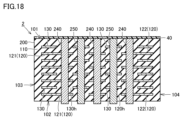
- 18 is a cross-sectional view of the multilayer ceramic capacitor of FIG. 17 as viewed from the direction of the arrows along line XVIII-XVIII.
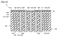
- 18 is a cross-sectional view of the multilayer ceramic capacitor of FIG. 17 as viewed from the direction of the arrows along line XIX-XIX.
- 18 is a cross-sectional view of the multilayer ceramic capacitor of FIG. 17, taken along the line XX-XX.
- Fig. 1 is a perspective view of a multilayer ceramic capacitor according to a first embodiment of the present invention, as viewed from the first main surface side.
- Fig. 2 is a plan view of the multilayer ceramic capacitor of Fig. 1, as viewed from direction II.
- Fig. 3 is a cross-sectional view of the multilayer ceramic capacitor of Fig. 2, as viewed from the direction of the arrows III-III.
- Fig. 4 is a plan view of a capacitor body.
- Fig. 5 is a cross-sectional view of the multilayer ceramic capacitor of Fig. 3, as viewed from the direction of the arrows V-V.
- Fig. 6 is a cross-sectional view of the multilayer ceramic capacitor of Fig. 3, as viewed from the direction of the arrows VI-VI.
- the multilayer ceramic capacitor 1 according to embodiment 1 of the present invention comprises a capacitor body 100, a plurality of first via conductors 140, a plurality of second via conductors 150, at least one first external electrode 20, and at least one second external electrode 30.
- the capacitor body 100 includes a plurality of first internal electrode layers 120 and a plurality of second internal electrode layers 130 that are alternately stacked in the stacking direction with dielectric layers 110 sandwiched between them, and has a first main surface 101 and a second main surface 102 that is located on the opposite side of the first main surface 101 in the stacking direction.
- the dielectric layer 110 may be made of any material, and may be made of, for example, a ceramic material mainly composed of BaTiO3 , CaTiO3 , SrTiO3 , SrZrO3 , or CaZrO3 .
- These main components may contain a minor component selected from the group consisting of Mn compounds, Fe compounds, Cr compounds, Co compounds, and Ni compounds, the minor component being contained in a smaller amount than the main component.
- the capacitor body 100 may have any shape.
- the capacitor body 100 has a rectangular parallelepiped shape as a whole.
- An overall rectangular parallelepiped shape is one that is not a perfect rectangular parallelepiped shape, for example, one in which the corners and edges of the rectangular parallelepiped are rounded, but has six surfaces and can be considered as a rectangular parallelepiped as a whole.
- the capacitor body 100 has a first main surface 101, a second main surface 102, a first side surface 103, a second side surface 104, a third side surface 105, and a fourth side surface 106.
- the first side surface 103 to the fourth side surface 106 of the capacitor body 100 constitute four side surfaces of the surface of the capacitor body 100 other than the first main surface 101 and the second main surface 102. That is, the capacitor body 100 further has the first side surface 103 to the fourth side surface 106, which are four side surfaces connecting the first main surface 101 and the second main surface 102.
- the first side surface 103 faces the second side surface 104
- the third side surface 105 faces the fourth side surface 106.
- the first side surface 103 to the fourth side surface 106 of the capacitor body 100 are perpendicular to each of the first main surface 101 and the second main surface 102, but they do not have to be perpendicular to each other.
- the dimensions of the capacitor body 100 are arbitrary, but for example, when viewed from the first main surface 101 side, the vertical dimension of the rectangle can be 0.3 mm to 3.0 mm, the horizontal dimension can be 0.3 mm to 3.0 mm, and the dimensions in the stacking direction of the dielectric layer 110, the first internal electrode layer 120, and the second internal electrode layer 130 can be 50 ⁇ m to 200 ⁇ m.
- the dimensions of the capacitor body 100 in the stacking direction refer to the thickness of the capacitor body 100.
- each of the first internal electrode layers 120 is composed of a plurality of first internal electrode parts that are spaced apart from each other in the same layer.
- each of the first internal electrode layers 120 is composed of a first internal electrode part 121 and a first internal electrode part 122 that are spaced apart from each other in the same layer.
- the first internal electrode part 121 and the first internal electrode part 122 have a line-symmetric shape.
- the shapes of the first internal electrode part 121 and the first internal electrode part 122 are not limited to line-symmetric shapes and may be asymmetric shapes.
- the number of first internal electrode parts arranged in the same layer is not limited to two and may be three or more.
- a plurality of first through holes 120h are formed to insert a plurality of second via conductors 150 described later.
- each of the first internal electrode layers 120 may be integrally formed in the same layer.
- each of the multiple second internal electrode layers 130 is integrally formed within the same layer.
- the second internal electrode layer 130 has a rectangular outer shape that is approximately the same as the first internal electrode layer 120.
- Each of the multiple second internal electrode layers 130 has multiple second through holes 130h formed therein to allow multiple first via conductors 140, which will be described later, to pass through.
- the material of the first internal electrode layer 120 and the second internal electrode layer 130 is arbitrary, and may contain, for example, a metal such as Ni, Cu, Ag, Pd, Pt, Fe, Ti, Cr, Sn, or Au, or an alloy containing these metals, as a main component.
- the first internal electrode layer 120 and the second internal electrode layer 130 may contain, as a common material, the same ceramic material as the dielectric ceramic contained in the dielectric layer 110. In that case, the proportion of the common material contained in the first internal electrode layer 120 and the second internal electrode layer 130 is, for example, 20 vol % or less.
- each of the first internal electrode layer 120 and the second internal electrode layer 130 is arbitrary, but can be, for example, about 0.3 ⁇ m or more and 1.0 ⁇ m or less.
- the number of layers of the first internal electrode layer 120 and the second internal electrode layer 130 is arbitrary, but can be, for example, about 10 layers or more and 150 layers or less in total.
- the first internal electrode layer 120 and the second internal electrode layer 130 face each other via the dielectric layer 110, forming a capacitance.
- the first internal electrode layer 120 and the second internal electrode layer 130 face each other via the dielectric layer 110, forming a capacitance.
- the multiple first via conductors 140 are provided inside the capacitor body 100 and are electrically connected to the multiple first internal electrode layers 120.
- the multiple first via conductors 140 pass through second through holes 130h formed in each of the multiple second internal electrode layers 130, and are insulated from the multiple second internal electrode layers 130.
- the multiple first via conductors 140 are arranged in multiple rows.
- each of the multiple first internal electrode portions is electrically connected to a corresponding multiple first via conductors 140 among the multiple first via conductors 140.
- the first internal electrode portion 121 is electrically connected to three corresponding first via conductors 140 arranged in a row.
- the first internal electrode portion 122 is electrically connected to the other three corresponding first via conductors 140 arranged in a row.
- Each of the multiple first via conductors 140 is provided inside the capacitor body 100 in a manner that extends in the stacking direction from the first main surface 101 to the second main surface 102 of the capacitor body 100. In other words, each of the multiple first via conductors 140 is exposed to the first main surface 101 of the capacitor body 100, but is not exposed to the second main surface 102. This makes it possible to prevent a short circuit from occurring between the electronic component arranged on the second main surface 102 side and the multilayer ceramic capacitor 1.
- the multiple second via conductors 150 are provided inside the capacitor body 100 and are electrically connected to the multiple second internal electrode layers 130.
- the multiple second via conductors 150 pass through first through holes 120h formed in each of the multiple first internal electrode layers 120, and are insulated from the multiple first internal electrode layers 120.
- the multiple second via conductors 150 are arranged in rows between the rows of the multiple first via conductors 140.
- the first via conductors 140 and the second via conductors 150 are arranged in a matrix.
- the second internal electrode layer 130 is electrically connected to three second via conductors 150 arranged in one row.
- Each of the multiple second via conductors 150 is provided inside the capacitor body 100 in a manner that extends in the stacking direction from the first main surface 101 to the second main surface 102 of the capacitor body 100. That is, each of the multiple second via conductors 150 is exposed to the first main surface 101 of the capacitor body 100, but is not exposed to the second main surface 102.
- the magnetic fields induced by the currents flowing through the first via conductors 140 and the second via conductors 150 cancel each other out, thereby lowering the equivalent series inductance (ESL) of the multilayer ceramic capacitor 1.
- the first via conductor 140 and the second via conductor 150 may have any shape, for example, a cylindrical shape.
- the diameter of the first via conductor 140 and the second via conductor 150 is, for example, about 30 ⁇ m or more and 150 ⁇ m or less.
- the distance between adjacent first via conductors 140 and second via conductors 150, more specifically, the distance between the center of the first via conductor 140 and the center of the second via conductor 150 is, for example, about 50 ⁇ m or more and 500 ⁇ m or less.
- the material of the first via conductor 140 and the second via conductor 150 is arbitrary, and for example, metals such as Ni, Cu, Ag, Pd, Pt, Fe, Ti, Cr, Sn, or Au, or alloys containing these metals, can be used.
- first external electrodes 20 and at least one second external electrode 30 are provided at intervals on the first main surface 101.
- the first external electrode 20 is composed of a first external electrode 21 and a first external electrode 22.
- the number of first external electrodes 20 is not limited to two, and may be one or more.
- the number of second external electrodes 30 is one, but may be two or more.
- Each of the multiple first external electrodes 20 extends in a rectangular shape.
- the shape of each of the multiple first external electrodes 20 is not limited to a rectangular shape, and may be a trapezoid, L-shape, U-shape, X-shape, T-shape, or the like.
- Each of at least one first external electrode 20 is electrically connected to a corresponding number of first via conductors 140 among the plurality of first via conductors 140.
- the first external electrode 21 is electrically connected to three corresponding first via conductors 140.
- the first external electrode 22 is electrically connected to the other three corresponding first via conductors 140.
- the connection relationship between the first external electrode 20 and the first via conductor 140 is not limited to the above, and it is sufficient that a corresponding number of first via conductors 140 are connected to each first external electrode 20.
- At least one second external electrode 30 extends in a rectangular shape.
- the shape of the second external electrode 30 is not limited to a rectangular shape, and may be a trapezoid, an L-shape, a U-shape, an X-shape, a T-shape, or the like.
- At least one second external electrode 30 is electrically connected to a corresponding number of second via conductors 150 among the plurality of second via conductors 150.
- one second external electrode 30 is electrically connected to all three second via conductors 150.
- the connection relationship between the second external electrode 30 and the second via conductors 150 is not limited to the above, and it is sufficient that a corresponding number of second via conductors 150 are connected to each second external electrode 30.
- the first external electrode 20 and the second external electrode 30 may be made of any material.
- the first external electrode 20 and the second external electrode 30 are plated electrodes formed by a plating process using a rotary plating method. Examples of materials that may form the plated electrodes include Cu, Ni, and Sn.
- the plated electrodes may be formed of a single layer or multiple layers.
- each of the first internal electrode layers 120 is composed of a first internal electrode portion 121 and a first internal electrode portion 122 that are spaced apart from each other in the same layer.
- Each of the second internal electrode layers 130 is integrally composed in the same layer.
- Each of the first internal electrode portion 121 and the first internal electrode portion 122 is electrically connected to a corresponding one of the first via conductors 140.
- Each of the first external electrode 21 and the first external electrode 22 is electrically connected to a corresponding one of the first internal electrode portions 121 and the first internal electrode portion 122.
- At least one second external electrode 30 is electrically connected to a corresponding one of the second via conductors 150.
- a capacitor functional section consisting of the first internal electrode section 121 and the second internal electrode layer 130 facing each other across the dielectric layer 110, and another capacitor functional section consisting of the first internal electrode section 122 and the second internal electrode layer 130 facing each other across the dielectric layer 110, can be arranged side by side at high density, thereby realizing a multilayer ceramic capacitor 1 with high capacitance density.
- each first external electrode 20 is electrically connected to a plurality of first via conductors 140 and each second external electrode 30 is electrically connected to a plurality of second via conductors 150
- each of the first external electrodes 20 and second external electrodes 30 can be easily connected to a connection terminal such as an IC and can be connected over the shortest distance compared to a case where each of the first via conductors 140 and second via conductors 150 is connected to a connection terminal such as an IC on a one-to-one basis.
- the present invention is particularly effective when the pitch between connection terminals such as ICs is short.
- the first via conductors 140 are arranged in a plurality of rows.
- the second via conductors 150 are arranged in rows between the rows of the first via conductors 140, thereby making it possible to reduce the ESL of the multilayer ceramic capacitor 1.
- the second external electrode 30 is disposed between the first external electrodes 20, so that the first external electrode 20 and the second external electrode 30 can be easily visually distinguished from each other regardless of the orientation of the multilayer ceramic capacitor 1.
- the orientation of the multilayer ceramic capacitor 1 means, for example, the vertical orientation shown in FIG. 2 and the horizontal orientation shown in FIG. 2 rotated 90°.
- the multilayer ceramic capacitor 1 according to the first embodiment of the present invention may be combined with the configuration of the second embodiment described later.
- an insulating layer 40 having a plurality of openings formed therein may be provided on the first main surface 101.
- At least one first external electrode 20 and at least one second external electrode 30 are provided on the insulating layer 40 at intervals from each other.
- Each first external electrode 20 is provided so as to cover a corresponding plurality of first via conductors 140 among the plurality of first via conductors 140 and at least one second via conductor 150 among the plurality of second via conductors 150.
- Each second external electrode 30 is provided so as to cover at least one first via conductor 140 among the plurality of first via conductors 140 and a corresponding plurality of second via conductors 150 among the plurality of second via conductors 150.
- Each first external electrode 20 is electrically connected to a corresponding plurality of first via conductors 140 through a corresponding opening among the plurality of openings.
- Each second external electrode 30 is electrically connected to a corresponding one of the multiple second via conductors 150 through a corresponding one of the multiple openings. This makes it possible to suppress the influence of the arrangement of the first via conductors 140 and the second via conductors 150 and ensure the freedom of arrangement of the first external electrode 20 and the second external electrode 30.
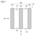
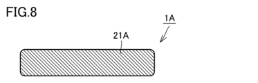
- FIG. 7 is a plan view of a multilayer ceramic capacitor according to a first modified example of embodiment 1 of the present invention.
- FIG. 8 is a side view of the multilayer ceramic capacitor of FIG. 7 as viewed from the direction of arrow VIII.
- FIG. 9 is a side view of the multilayer ceramic capacitor of FIG. 7 as viewed from the direction of arrow IX.
- the multilayer ceramic capacitor 1A includes a plurality of first external electrodes 20A and at least one second external electrode 30A.
- the first external electrode 20A is composed of a first external electrode 21A and a first external electrode 22A.
- Each of the plurality of first external electrodes 20A extends from the first main surface 101 onto at least one of the four side surfaces.
- At least one second external electrode 30A extends from the first main surface 101 onto at least one of the four side surfaces.
- the first external electrode 21A is formed from the first main surface 101 to the first side surface 103, the third side surface 105, and the fourth side surface 106.
- the first external electrode 21A covers the ridge portion between the first main surface 101 and the first side surface 103.
- the first external electrode 22A is formed from the first main surface 101 to the second side surface 104, the third side surface 105, and the fourth side surface 106.
- the first external electrode 22A covers the ridge portion between the first main surface 101 and the second side surface 104.
- the second external electrode 30A is formed from the first main surface 101 to the third side surface 105 and the fourth side surface 106.
- the corners or ridges of the capacitor body 100 can be covered with the first external electrode 20A and the second external electrode 30A, which can prevent cracks or chips from occurring at the corners or ridges of the capacitor body 100.
- the corners or ridges of the capacitor body 100 can be covered with the first external electrode 20A and the second external electrode 30A, which can prevent cracks or chips from occurring at the corners or ridges of the capacitor body 100.
- by contacting a probe with each of the first external electrode 20A and the second external electrode 30A formed on the side surface of the capacitor body 100 it is possible to measure the electrical characteristics of the multilayer ceramic capacitor 1A.
- the first external electrode 20A and the second external electrode 30A may be formed, for example, by a sputtering method, a vapor deposition method, or a method of baking metal powder or metal powder paste.
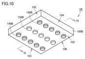
- FIG. 10 is a perspective view of a multilayer ceramic capacitor according to a second modified example of the first embodiment of the present invention, viewed from the second main surface side.
- FIG. 11 is a cross-sectional view of the multilayer ceramic capacitor of FIG. 10, viewed from the direction of the arrows along line XI-XI.
- the multilayer ceramic capacitor 1B according to the second modified example of the first embodiment of the present invention includes a plurality of first via conductors 140B and a plurality of second via conductors 150B provided inside the capacitor body 100B.
- the first via conductors 140B and the second via conductors 150B are arranged in a matrix.
- Each of the multiple first via conductors 140B is exposed to the first principal surface 101 and also to the second principal surface 102 of the capacitor body 100B. Specifically, each of the multiple first via conductors 140B is arranged to penetrate the capacitor body 100B in the stacking direction. One end of each of the multiple first via conductors 140B in the stacking direction is connected to the first external electrode 20, and the other end protrudes from the second principal surface 102. Note that the other end of each of the multiple first via conductors 140B does not necessarily have to protrude from the second principal surface 102, and may be located flush with the second principal surface 102.
- Each of the multiple second via conductors 150B is exposed to the first principal surface 101 and also to the second principal surface 102 of the capacitor body 100B. Specifically, each of the multiple second via conductors 150B is arranged to penetrate the capacitor body 100B in the stacking direction. One end of each of the multiple second via conductors 150B in the stacking direction is connected to the second external electrode 30, and the other end protrudes from the second principal surface 102. Note that the other end of each of the multiple second via conductors 150B does not necessarily have to protrude from the second principal surface 102, and may be located flush with the second principal surface 102.
- each of the multiple first via conductors 140B and the multiple second via conductors 150B is exposed on the second principal surface 102 side. This makes it possible to electrically connect the electronic component connected to the first principal surface 101 side and the electronic component connected to the second principal surface 102 side via the multilayer ceramic capacitor 1B.
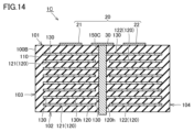
- FIG. 12 is a perspective view of a multilayer ceramic capacitor according to a third modified example of the first embodiment of the present invention, viewed from the second main surface side.
- FIG. 13 is a cross-sectional view of the multilayer ceramic capacitor of FIG. 12, viewed from the direction of the arrows along line XIII-XIII.
- FIG. 14 is a cross-sectional view of the multilayer ceramic capacitor of FIG. 12, viewed from the direction of the arrows along line XIV-XIV.
- the multilayer ceramic capacitor 1C according to the third modified example of the first embodiment of the present invention includes a plurality of first via conductors 140C and a plurality of second via conductors 150C provided inside the capacitor body 100C.
- the first via conductors 140C and the second via conductors 150C are arranged at different positions in the column direction.
- each of the plurality of first via conductors 140C and the plurality of second via conductors 150C is exposed on the second principal surface 102 side. This makes it possible to electrically connect an electronic component connected to the first principal surface 101 side and an electronic component connected to the second principal surface 102 side via the multilayer ceramic capacitor 1C.
- the multilayer ceramic capacitor according to the second embodiment of the present invention differs from the multilayer ceramic capacitor according to the first embodiment of the present invention mainly in the arrangement of the first external electrodes, the second external electrodes, the first via conductors, and the second via conductors, and in further including an insulating layer, and therefore the same components as those in the multilayer ceramic capacitor according to the first embodiment of the present invention will be given the same reference numerals and description thereof will not be repeated.
- FIG. 15 is a perspective view of a multilayer ceramic capacitor according to embodiment 2 of the present invention, as viewed from the first main surface side.
- FIG. 16 is an exploded perspective view showing the configuration of a multilayer ceramic capacitor according to embodiment 2 of the present invention.
- FIG. 17 is a perspective view of the multilayer ceramic capacitor of FIG. 16, as viewed from the XVII direction.
- FIG. 18 is a cross-sectional view of the multilayer ceramic capacitor of FIG. 17, as viewed from the direction of the XVIII-XVIII arrows.
- FIG. 19 is a cross-sectional view of the multilayer ceramic capacitor of FIG. 17, as viewed from the direction of the XIX-XIX arrows.
- FIG. 20 is a cross-sectional view of the multilayer ceramic capacitor of FIG. 17, as viewed from the direction of the XX-XX arrows.
- the multilayer ceramic capacitor 2 according to the second embodiment of the present invention comprises a capacitor body 200, a plurality of first via conductors 240, a plurality of second via conductors 250, a plurality of first external electrodes 20 and a plurality of second external electrodes 30, and an insulating layer 40.
- the multilayer ceramic capacitor 2 includes a plurality of first via conductors 240 and a plurality of second via conductors 250 provided inside the capacitor body 200.
- the plurality of first via conductors 240 and the plurality of second via conductors 250 are arranged alternately in both the row direction and the column direction.
- Each of the multiple first via conductors 240 is exposed to the first main surface 101 of the capacitor body 200 and also to the second main surface 102. Specifically, each of the multiple first via conductors 240 is arranged to penetrate the capacitor body 200 in the stacking direction. One end of each of the multiple first via conductors 240 in the stacking direction is located flush with the first main surface 101, and the other end protrudes from the second main surface 102. Note that the other end of each of the multiple first via conductors 240 does not necessarily have to protrude from the second main surface 102, and may be located flush with the second main surface 102.
- Each of the multiple second via conductors 250 is exposed to the first main surface 101 and also to the second main surface 102 of the capacitor body 200. Specifically, each of the multiple second via conductors 250 is arranged to penetrate the capacitor body 200 in the stacking direction. One end of each of the multiple second via conductors 250 in the stacking direction is located flush with the first main surface 101, and the other end protrudes from the second main surface 102. Note that the other end of each of the multiple second via conductors 250 does not necessarily have to protrude from the second main surface 102, and may be located flush with the second main surface 102.
- the insulating layer 40 is provided on the first main surface 101.
- the insulating layer 40 covers the entire first main surface 101.
- the insulating layer 40 has a plurality of first openings 41h and a plurality of second openings 42h formed in the first main surface 101.
- the insulating layer 40 can be made of ceramic.
- the insulating layer 40 is made of ceramic , at least one selected from the group consisting of Al2O3 , PZT, SiC, SiO2 , and MgO is used as the material constituting the insulating layer 40.
- the insulating layer 40 is made of ceramic, the mechanical strength of the multilayer ceramic capacitor 2 against stress can be improved.
- the insulating layer 40 is made of ceramic, it is preferable that the grain size of the ceramic contained in the dielectric layer 110 is smaller than that of the ceramic contained in the insulating layer 40.
- the insulating layer 40 may be formed by aerosol deposition (AD) or a thermal spray method such as cold spray, or by chemical vapor deposition (CVD).
- AD aerosol deposition
- CVD chemical vapor deposition
- the material constituting the insulating layer 40 may include at least one selected from the group consisting of epoxy resin, silicone resin, fluororesin, phenolic resin, urea resin, melamine resin, unsaturated polyester resin, barium titanate, alumina, silica, yttria, and zirconia.
- the material constituting the insulating layer 40 is preferably a thermosetting epoxy resin using a metal oxide used as a solder resist, silicone resin, fluororesin, phenolic resin, melamine resin, barium titanate, alumina, silica, or the like.
- the insulating layer 40 When the insulating layer 40 is made of resin, it can be formed by using a spraying device or a dipping device as a forming means. Alternatively, the insulating layer 40 may be formed by attaching it to the first main surface 101 of the capacitor body 200, or the insulating layer 40 may be formed by a screen printing method.
- the insulating layer 40 is adhered to the first main surface 101 of the multilayer ceramic capacitor 2 by thermally curing or drying the insulating layer 40 depending on the physical properties of the insulating material.
- the first external electrode 20 is composed of a first external electrode 21 and a first external electrode 22.
- the number of the first external electrodes 20 is not limited to two, and may be one or more.
- the first external electrode 21 and the first external electrode 22 have a rectangular shape, and are respectively located above corners located on diagonals of the rectangular first main surface 101.
- the second external electrode 30 is composed of a second external electrode 31 and a second external electrode 32.
- the number of the second external electrodes 30 is not limited to two, and may be one or more.
- the second external electrode 31 and the second external electrode 32 have a rectangular shape, and are respectively located above corners located on other diagonals of the rectangular first main surface 101.
- each of the first external electrode 21 and the first external electrode 22 is arranged to cover two corresponding first via conductors 240 out of the multiple first via conductors 240 and two corresponding second via conductors 250 out of the multiple second via conductors 250.
- the number of corresponding first via conductors 240 covered by each of the first external electrode 21 and the first external electrode 22 is not limited to two, and may be three or more.
- the number of second via conductors 250 covered by each of the first external electrode 21 and the first external electrode 22 is not limited to two, and may be one or more.
- each of the second external electrode 31 and the second external electrode 32 is arranged to cover two of the multiple first via conductors 240 and two corresponding second via conductors 250 of the multiple second via conductors 250.
- the number of first via conductors 240 covered by each of the second external electrode 31 and the second external electrode 32 is not limited to two, and may be one or more.
- the number of corresponding second via conductors 250 covered by each of the second external electrode 31 and the second external electrode 32 is not limited to two, and may be three or more.
- Each of the first external electrode 21 and the first external electrode 22 is electrically connected to two corresponding first via conductors 240 through two corresponding first openings 41h among the multiple openings. Specifically, a portion of each of the first external electrode 21 and the first external electrode 22 is provided within the first opening 41h and is connected to one end of the first via conductor 240 in the stacking direction.
- each of the second external electrodes 31 and 32 is electrically connected to two corresponding second via conductors 250 through two corresponding second openings 42h among the multiple openings. Specifically, a portion of each of the second external electrodes 31 and 32 is provided within the second opening 42h and connected to one end of the second via conductor 250 in the stacking direction.
- the connection relationship between the second external electrodes 30 and the second via conductors 250 is not limited to the above, and it is sufficient that multiple corresponding second via conductors 250 are connected to each second external electrode 30.
- the first via conductors 240 and the second via conductors 250 are arranged alternately in both the row and column directions. This allows the ESL of the multilayer ceramic capacitor 2 to be further reduced compared to the multilayer ceramic capacitor 1 according to the first embodiment.
- the first external electrodes 20 are electrically connected to the corresponding first via conductors 240 through the corresponding first openings 41h of the multiple openings.
- At least one second external electrode 30 is electrically connected to the corresponding second via conductors 250 through the corresponding second openings 42h of the multiple openings. This makes it possible to suppress the influence of the arrangement of the first via conductors 240 and the second via conductors 250 and ensure the freedom of arrangement of the first external electrode 20 and the second external electrode 30.
- the first external electrode 20 and the second external electrode 30 can be arranged at any position, and the first external electrode 20 and the first via conductor 240 corresponding to the first external electrode 20 can be electrically connected, and the second external electrode 30 and the second via conductor 250 corresponding to the second external electrode 30 can be electrically connected.
- each of the first internal electrode layers 120 is composed of a plurality of first internal electrode portions that are spaced apart from each other within the same layer, but this is not limited thereto, and each of the first internal electrode layers 120 may be integrally formed within the same layer.
- the capacitor body 200 has only one capacitor functional portion.
- a capacitor body including a plurality of first internal electrode layers and a plurality of second internal electrode layers alternately stacked one by one in a stacking direction with a dielectric layer sandwiched therebetween, the capacitor body having a first main surface and a second main surface located on the opposite side of the first main surface in the stacking direction; a plurality of first via conductors provided inside the capacitor body and electrically connected to the plurality of first internal electrode layers; a plurality of second via conductors provided inside the capacitor body and electrically connected to the plurality of second internal electrode layers; an insulating layer provided on the first main surface and having a plurality of openings; at least one first external electrode and at least one second external electrode provided on the insulating layer and spaced apart from each other; the at least one first external electrode is provided to cover corresponding ones of the first via conductors and at least one second via conductor of the second via conductors; the at least one first external electrode is electrically connected to the corresponding first via conductors through a corresponding one of
- ⁇ 2> The multilayer ceramic capacitor described in ⁇ 1>, wherein the at least one second external electrode is arranged to cover at least one first via conductor among the plurality of first via conductors and the corresponding plurality of second via conductors among the plurality of second via conductors.
- Each of the plurality of first internal electrode layers is composed of a plurality of first internal electrode portions that are spaced apart from each other within the same layer, Each of the plurality of second internal electrode layers is integrally formed within the same layer, each of the first internal electrode portions is electrically connected to a corresponding one of the first via conductors;
- the at least one first external electrode includes a plurality of first external electrodes, The multilayer ceramic capacitor described in ⁇ 1> or ⁇ 2>, wherein each of the plurality of first external electrodes is electrically connected to a plurality of first via conductors that are electrically connected to a corresponding one of the plurality of first internal electrode portions.
- ⁇ 4> The multilayer ceramic capacitor according to any one of ⁇ 1> to ⁇ 3>, wherein each of the plurality of first via conductors and the plurality of second via conductors is exposed on a second main surface side.
- the first via conductors are arranged in a plurality of rows, The multilayer ceramic capacitor according to any one of ⁇ 1> to ⁇ 4>, wherein the second via conductors are arranged in rows between the rows of the first via conductors.
- ⁇ 6> The multilayer ceramic capacitor according to any one of ⁇ 1> to ⁇ 4>, wherein the plurality of first via conductors and the plurality of second via conductors are alternately arranged in both the row direction and the column direction.
- 1, 1A, 1B, 1C, 2 multilayer ceramic capacitor; 20, 20A, 21, 21A, 22, 22A: first external electrode; 30, 30A, 31, 32: second external electrode; 40: insulating layer; 41h: first opening; 42h: second opening; 100, 100B, 100C, 200: capacitor body; 101: first main surface; 102: second main surface; 103: First side, 104 second side, 105 third side, 106 fourth side, 110 dielectric layer, 120 first internal electrode layer, 120h first through hole, 121, 122 first internal electrode portion, 130 second internal electrode layer, 130h second through hole, 140, 140B, 140C, 240 first via conductor, 150, 150B, 150C, 250 second via conductor.
Landscapes
- Engineering & Computer Science (AREA)
- Power Engineering (AREA)
- Manufacturing & Machinery (AREA)
- Microelectronics & Electronic Packaging (AREA)
- Chemical & Material Sciences (AREA)
- Ceramic Engineering (AREA)
- Inorganic Chemistry (AREA)
- Ceramic Capacitors (AREA)
- Fixed Capacitors And Capacitor Manufacturing Machines (AREA)
Abstract
Description
本発明は、積層セラミックコンデンサに関する。 The present invention relates to a multilayer ceramic capacitor.
配線基板内蔵用電子部品の構成を開示した先行技術文献として、特開2009-295687号公報(特許文献1)がある。特許文献1に記載された配線基板内蔵用電子部品は、セラミック焼結体と、外部電極とを備える。セラミック焼結体は、主面および裏面を有する。外部電極は、セラミック焼結体の主面および裏面の少なくとも一方の上に配置され、メタライズ金属層の表面に銅めっき層を形成してなる。セラミック焼結体には、セラミック誘電体層を介して複数の内部電極が積層配置され、複数の内部電極に接続された複数のコンデンサ内ビア導体が設けられている。外部電極が、複数のコンデンサ内ビア導体における主面側および裏面側の少なくとも一方の端部に接続されている。複数のコンデンサ内ビア導体が全体としてアレイ状に配置されている。
JP 2009-295687 A (Patent Document 1) is a prior art document that discloses the configuration of an electronic component for incorporation into a wiring board. The electronic component for incorporation into a wiring board described in
積層セラミックコンデンサには、ビア導体の配置の影響を抑制して外部電極の配置の自由度を確保することが求められる場合がある。 In multilayer ceramic capacitors, it is sometimes necessary to suppress the effect of via conductor placement and ensure freedom in the placement of external electrodes.
本発明は上記の課題に鑑みてなされたものであって、外部電極の配置の自由度を確保することができる、積層セラミックコンデンサを提供することを目的とする。 The present invention was made in consideration of the above problems, and aims to provide a multilayer ceramic capacitor that ensures freedom in the arrangement of external electrodes.
本発明に基づく積層セラミックコンデンサは、コンデンサ本体と、複数の第1ビア導体と、複数の第2ビア導体と、絶縁層と、少なくとも1つの第1外部電極および少なくとも1つの第2外部電極とを備える。コンデンサ本体は、誘電体層を挟んで1層ずつ交互に積層方向に積層された複数の第1内部電極層および複数の第2内部電極層を含み、第1主面および第1主面とは上記積層方向の反対側に位置する第2主面を有する。複数の第1ビア導体は、コンデンサ本体の内部に設けられ、複数の第1内部電極層と電気的に接続されている。複数の第2ビア導体は、コンデンサ本体の内部に設けられ、複数の第2内部電極層と電気的に接続されている。絶縁層は、第1主面上に設けられ、複数の開口部が形成されている。少なくとも1つの第1外部電極および少なくとも1つの第2外部電極は、絶縁層上において互いに間隔をあけて設けられている。少なくとも1つの第1外部電極は、複数の第1ビア導体のうちの対応する複数の第1ビア導体、および、複数の第2ビア導体うちの少なくとも1つの第2ビア導体を覆うように設けられている。少なくとも1つの第1外部電極は、複数の開口部のうちの対応する開口部を通じて対応する複数の第1ビア導体と電気的に接続されている。少なくとも1つの第2外部電極は、複数の開口部のうちの対応する開口部を通じて対応する複数の第2ビア導体と電気的に接続されている。 The multilayer ceramic capacitor according to the present invention comprises a capacitor body, a plurality of first via conductors, a plurality of second via conductors, an insulating layer, and at least one first external electrode and at least one second external electrode. The capacitor body includes a plurality of first internal electrode layers and a plurality of second internal electrode layers that are alternately stacked in a stacking direction with a dielectric layer sandwiched therebetween, and has a first main surface and a second main surface located on the opposite side of the stacking direction from the first main surface. The plurality of first via conductors are provided inside the capacitor body and are electrically connected to the plurality of first internal electrode layers. The plurality of second via conductors are provided inside the capacitor body and are electrically connected to the plurality of second internal electrode layers. The insulating layer is provided on the first main surface, and has a plurality of openings formed therein. The at least one first external electrode and the at least one second external electrode are provided on the insulating layer at intervals from each other. The at least one first external electrode is provided so as to cover a corresponding plurality of first via conductors among the plurality of first via conductors and at least one second via conductor among the plurality of second via conductors. At least one first external electrode is electrically connected to a corresponding number of first via conductors through a corresponding opening of the plurality of openings. At least one second external electrode is electrically connected to a corresponding number of second via conductors through a corresponding opening of the plurality of openings.
本発明によれば、ビア導体の配置の影響を抑制して外部電極の配置の自由度を確保することができる。 According to the present invention, it is possible to suppress the influence of the arrangement of the via conductors and ensure the freedom of arrangement of the external electrodes.
以下、本発明の各実施形態に係る積層セラミックコンデンサについて図を参照して説明する。以下の実施形態の説明においては、図中の同一または相当部分には同一符号を付して、その説明は繰り返さない。 Below, the multilayer ceramic capacitor according to each embodiment of the present invention will be described with reference to the drawings. In the following description of the embodiments, the same or corresponding parts in the drawings will be given the same reference numerals, and the description will not be repeated.
(実施形態1)
図1は、本発明の実施形態1に係る積層セラミックコンデンサを第1主面側から見た斜視図である。図2は、図1の積層セラミックコンデンサをII方向から見た平面図である。図3は、図2の積層セラミックコンデンサをIII-III線矢印方向から見た断面図である。図4は、コンデンサ本体の平面図である。図5は、図3の積層セラミックコンデンサをV-V線矢印方向から見た断面図である。図6は、図3の積層セラミックコンデンサをVI-VI線矢印方向から見た断面図である。
(Embodiment 1)
Fig. 1 is a perspective view of a multilayer ceramic capacitor according to a first embodiment of the present invention, as viewed from the first main surface side. Fig. 2 is a plan view of the multilayer ceramic capacitor of Fig. 1, as viewed from direction II. Fig. 3 is a cross-sectional view of the multilayer ceramic capacitor of Fig. 2, as viewed from the direction of the arrows III-III. Fig. 4 is a plan view of a capacitor body. Fig. 5 is a cross-sectional view of the multilayer ceramic capacitor of Fig. 3, as viewed from the direction of the arrows V-V. Fig. 6 is a cross-sectional view of the multilayer ceramic capacitor of Fig. 3, as viewed from the direction of the arrows VI-VI.
図1~図6に示すように、本発明の実施形態1に係る積層セラミックコンデンサ1は、コンデンサ本体100と、複数の第1ビア導体140と、複数の第2ビア導体150と、少なくとも1つの第1外部電極20および少なくとも1つの第2外部電極30とを備える。
As shown in Figures 1 to 6, the multilayer
図3に示すように、コンデンサ本体100は、誘電体層110を挟んで1層ずつ交互に積層方向に積層された複数の第1内部電極層120および複数の第2内部電極層130を含み、第1主面101および第1主面101とは上記積層方向の反対側に位置する第2主面102を有する。
As shown in FIG. 3, the
誘電体層110の材質は任意であり、たとえば、BaTiO3、CaTiO3、SrTiO3、SrZrO3、または、CaZrO3などを主成分とするセラミック材料からなる。これらの主成分に、Mn化合物、Fe化合物、Cr化合物、Co化合物およびNi化合物からなる群から選ばれる、主成分よりも含有量の少ない副成分が添加されていてもよい。
The
コンデンサ本体100の形状は任意である。本実施形態では、コンデンサ本体100は、全体として直方体の形状を有する。全体として直方体の形状とは、たとえば、直方体の角部および稜線部が丸みを帯びている形状のように、完全な直方体の形状ではないが、6つの表面を有し、全体として直方体ととらえることができる形状のことである。したがって、コンデンサ本体100は、第1主面101と、第2主面102と、第1側面103と、第2側面104と、第3側面105と、第4側面106とを備える。
The
コンデンサ本体100の第1側面103~第4側面106は、コンデンサ本体100の表面のうち、第1主面101および第2主面102以外の面である4つの側面を構成している。すなわち、コンデンサ本体100は、第1主面101と第2主面102とを繋ぐ4つの側面である第1側面103~第4側面106をさらに有する。第1側面103は、第2側面104と相対し、第3側面105は、第4側面106と相対している。本実施形態において、コンデンサ本体100の第1側面103~第4側面106は、第1主面101および第2主面102のそれぞれと直交しているが、直交していなくてもよい。
The
コンデンサ本体100の寸法は任意であるが、たとえば、第1主面101側から見て、矩形の縦方向の寸法を0.3mm以上3.0mm以下、横方向の寸法を0.3mm以上3.0mm以下、誘電体層110、第1内部電極層120および第2内部電極層130の積層方向における寸法を50μm以上200μm以下とすることができる。上記積層方向におけるコンデンサ本体100の寸法とは、コンデンサ本体100の厚みのことである。
The dimensions of the
図3および図5に示すように、複数の第1内部電極層120の各々は、同一層内において互いに離間している複数の第1内部電極部で構成されている。本実施形態においては、複数の第1内部電極層120の各々は、同一層内において互いに離間している、第1内部電極部121および第1内部電極部122で構成されている。第1内部電極部121および第1内部電極部122は、線対称の形状を有している。ただし、第1内部電極部121および第1内部電極部122の形状は、線対称の形状に限られず、非対称の形状であってもよい。また、同一層内に配置される第1内部電極部の数は、2つに限られず、3つ以上でもよい。複数の第1内部電極層120の各々には、後述する複数の第2ビア導体150を挿通させるために、複数の第1貫通孔120hが形成されている。なお、複数の第1内部電極層120の各々は、同一層内において一体で構成されていてもよい。
3 and 5, each of the first
図3および図6に示すように、複数の第2内部電極層130の各々は、同一層内において一体で構成されている。第2内部電極層130は、第1内部電極層120と略同一の矩形状の外形を有している。複数の第2内部電極層130の各々には、後述する複数の第1ビア導体140を挿通させるために、複数の第2貫通孔130hが形成されている。
As shown in Figures 3 and 6, each of the multiple second internal electrode layers 130 is integrally formed within the same layer. The second
第1内部電極層120および第2内部電極層130の材質は、任意であり、たとえば、Ni、Cu、Ag、Pd、Pt、Fe、Ti、Cr、Sn若しくはAuなどの金属、またはそれらの金属を含む合金などを主成分として含有している。第1内部電極層120および第2内部電極層130は、共材として、誘電体層110に含まれる誘電体セラミックと同じセラミック材料を含んでいてもよい。その場合、第1内部電極層120および第2内部電極層130に含まれる共材の割合は、たとえば、20vol%以下である。
The material of the first
第1内部電極層120および第2内部電極層130の各々の厚さは任意であるが、たとえば、0.3μm以上1.0μm以下程度とすることができる。第1内部電極層120および第2内部電極層130の層数は任意であるが、両方を併せて、たとえば、10層以上150層以下程度とすることができる。
The thickness of each of the first
積層セラミックコンデンサ1においては、第1内部電極層120と第2内部電極層130とが誘電体層110を介して対向することにより静電容量が形成される。複数の第1内部電極部が同一の第2内部電極層130と対向しつつ互いに間隔をあけて配置されていることにより、複数のコンデンサ機能部が高密度に並設された容量密度の高い積層セラミックコンデンサを実現することができる。
In the multilayer
図3~図6に示すように、複数の第1ビア導体140は、コンデンサ本体100の内部に設けられ、複数の第1内部電極層120と電気的に接続されている。複数の第1ビア導体140は、複数の第2内部電極層130の各々に形成されている第2貫通孔130hを挿通しており、複数の第2内部電極層130とは絶縁されている。本実施形態においては、複数の第1ビア導体140は、複数列に並んで配置されている。
As shown in Figures 3 to 6, the multiple first via
図3および図5に示すように、複数の第1内部電極部の各々は、複数の第1ビア導体140のうちの対応する複数の第1ビア導体140と電気的に接続されている。本実施形態においては、第1内部電極部121は、1列に並んだ対応する3つの第1ビア導体140と電気的に接続されている。第1内部電極部122は、1列に並んだ対応する他の3つの第1ビア導体140と電気的に接続されている。
As shown in Figures 3 and 5, each of the multiple first internal electrode portions is electrically connected to a corresponding multiple first via
複数の第1ビア導体140の各々は、コンデンサ本体100の第1主面101から第2主面102に向けて上記積層方向に延伸する態様でコンデンサ本体100の内部に設けられている。すなわち、複数の第1ビア導体140の各々は、コンデンサ本体100の第1主面101に露出しており、第2主面102には露出していない。これにより、第2主面102側に配置される電子部品と積層セラミックコンデンサ1との短絡が生ずることを抑制することができる。
Each of the multiple first via
図3~図6に示すように、複数の第2ビア導体150は、コンデンサ本体100の内部に設けられ、複数の第2内部電極層130と電気的に接続されている。複数の第2ビア導体150は、複数の第1内部電極層120の各々に形成されている第1貫通孔120hを挿通しており、複数の第1内部電極層120とは絶縁されている。本実施形態においては、複数の第2ビア導体150は、複数の第1ビア導体140が並んだ列同士の間で列状に並んで配置されている。第1ビア導体140と第2ビア導体150とは、行列状に並んで配置されている。第2内部電極層130は、1列に並んだ3つの第2ビア導体150と電気的に接続されている。
As shown in Figures 3 to 6, the multiple second via
複数の第2ビア導体150の各々は、コンデンサ本体100の第1主面101から第2主面102に向けて上記積層方向に延伸する態様でコンデンサ本体100の内部に設けられている。すなわち、複数の第2ビア導体150の各々は、コンデンサ本体100の第1主面101に露出しており、第2主面102には露出していない。
Each of the multiple second via
複数の第1ビア導体140および複数の第2ビア導体150が上記のように交互に列状に配置されていることにより、第1ビア導体140および第2ビア導体150をそれぞれ流れる電流によって誘導される磁界が相互相殺されることにより、積層セラミックコンデンサ1の等価直列インダクタンス(ESL)を低くすることができる。
By arranging the multiple first via
第1ビア導体140および第2ビア導体150の形状は任意であり、たとえば、円柱状とすることができる。その場合の第1ビア導体140および第2ビア導体150の直径は、たとえば、30μm以上150μm以下程度である。また、隣り合う第1ビア導体140と第2ビア導体150との間の距離、より詳しくは、第1ビア導体140の中心と第2ビア導体150の中心との間の距離は、たとえば、50μm以上500μm以下程度である。
The first via
第1ビア導体140および第2ビア導体150の材質は、任意であり、たとえば、Ni、Cu、Ag、Pd、Pt、Fe、Ti、Cr、Sn若しくはAuなどの金属、またはそれらの金属を含む合金などを用いることが可能である。
The material of the first via
図1~図3に示すように、複数の第1外部電極20および少なくとも1つの第2外部電極30は、第1主面101上において互いに間隔をあけて設けられている。本実施形態においては、第1外部電極20は、第1外部電極21および第1外部電極22で構成されている。ただし、第1外部電極20の数は、2つに限られず、1つ以上であればよい。本実施形態においては、第2外部電極30の数は、1つであるが、2つ以上でもよい。
As shown in Figures 1 to 3, a plurality of first
複数の第1外部電極20の各々は、矩形状に延在している。ただし、複数の第1外部電極20の各々の形状は、矩形状に限られず、台形状、L字状、U字状、X字状またはT字状などでもよい。
Each of the multiple first
少なくとも1つの第1外部電極20の各々は、複数の第1ビア導体140のうちの対応する複数の第1ビア導体140と電気的に接続されている。本実施形態においては、第1外部電極21は、対応する3つの第1ビア導体140と電気的に接続されている。第1外部電極22は、対応する他の3つの第1ビア導体140と電気的に接続されている。ただし、第1外部電極20と第1ビア導体140との接続関係は、上記に限られず、各第1外部電極20に対して、対応する複数の第1ビア導体140が接続されていればよい。
Each of at least one first
少なくとも1つの第2外部電極30は、矩形状に延在している。ただし、第2外部電極30の形状は、矩形状に限られず、台形状、L字状、U字状、X字状またはT字状などでもよい。
At least one second
少なくとも1つの第2外部電極30は、複数の第2ビア導体150のうちの対応する複数の第2ビア導体150と電気的に接続されている。本実施形態においては、1つの第2外部電極30は、3つの第2ビア導体150の全てと電気的に接続されている。ただし、第2外部電極30と第2ビア導体150との接続関係は、上記に限られず、各第2外部電極30に対して、対応する複数の第2ビア導体150が接続されていればよい。
At least one second
第1外部電極20および第2外部電極30の材質は任意である。本実施形態においては、第1外部電極20および第2外部電極30は、回転めっき法によるめっき処理で形成されるめっき電極である。めっき電極を構成する材料として、Cu、NiおよびSnなどが挙げられる。めっき電極は、単層で構成されていてもよいし、複数層で構成されていてもよい。
The first
本発明の実施形態1に係る積層セラミックコンデンサ1は、複数の第1内部電極層120の各々は、同一層内において互いに離間している第1内部電極部121および第1内部電極部122で構成されている。複数の第2内部電極層130の各々は、同一層内において一体で構成されている。第1内部電極部121および第1内部電極部122の各々は、複数の第1ビア導体140のうちの対応する複数の第1ビア導体140と電気的に接続されている。第1外部電極21および第1外部電極22の各々は、第1内部電極部121および第1内部電極部122のうちの対応する第1内部電極部と電気的に接続されている複数の第1ビア導体140と電気的に接続されている。少なくとも1つの第2外部電極30は、複数の第2ビア導体150のうちの対応する複数の第2ビア導体150と電気的に接続されている。
In the multilayer
これにより、第2外部電極30を接地しつつ第1外部電極21および第1外部電極22の各々を電位の異なる電源に接続することによって、誘電体層110を挟んで対向する第1内部電極部121と第2内部電極層130とからなるコンデンサ機能部と、誘電体層110を挟んで対向する第1内部電極部122と第2内部電極層130とからなる他のコンデンサ機能部とを、高密度に並設することができ、容量密度の高い積層セラミックコンデンサ1を実現することができる。
By connecting the first
また、各第1外部電極20が複数の第1ビア導体140と電気的に接続され、各第2外部電極30が複数の第2ビア導体150と電気的に接続されていることにより、第1ビア導体140および第2ビア導体150の各々とICなどの接続端子を1対1で接続する場合に比較して、第1外部電極20および第2外部電極30の各々とICなどの接続端子を容易に接続することができるとともに、最短距離で接続することができる。特に、ICなどの接続端子同士のピッチが短い場合に、本発明が効果的である。
Furthermore, since each first
本発明の実施形態1に係る積層セラミックコンデンサ1においては、複数の第1ビア導体140は、複数列に並んで配置されている。複数の第2ビア導体150は、複数の第1ビア導体140が並んだ列同士の間で列状に並んで配置されている、これにより、積層セラミックコンデンサ1のESLを低くすることができる。
In the multilayer
本発明の実施形態1に係る積層セラミックコンデンサ1においては、第1外部電極20同士の間に第2外部電極30が配置されていることにより、積層セラミックコンデンサ1の向きによらず、第1外部電極20と第2外部電極30とを視覚的に容易に識別することができる。ここで、積層セラミックコンデンサ1の向きとは、たとえば、図2に示す状態を縦向き、図2の積層セラミックコンデンサ1を90°回転させた状態を横向きとした場合の、縦向きと横向きとを意味する。
In the multilayer
本発明の実施形態1に係る積層セラミックコンデンサ1において、後述する実施形態2の構成と組み合わせてもよい。具体的には、第1主面101上に、複数の開口部が形成された絶縁層40が設けられていてもよい。少なくとも1つの第1外部電極20および少なくとも1つの第2外部電極30は、絶縁層40上において互いに間隔をあけて設けられる。各第1外部電極20は、複数の第1ビア導体140のうちの対応する複数の第1ビア導体140、および、複数の第2ビア導体150うちの少なくとも1つの第2ビア導体150を覆うように設けられている。各第2外部電極30は、複数の第1ビア導体140のうちの少なくとも1つの第1ビア導体140、および、複数の第2ビア導体150うちの対応する複数の第2ビア導体150を覆うように設けられている。各第1外部電極20は、複数の開口部のうちの対応する開口部を通じて対応する複数の第1ビア導体140と電気的に接続されている。各第2外部電極30は、複数の開口部のうちの対応する開口部を通じて対応する複数の第2ビア導体150と電気的に接続されている。これにより、第1ビア導体140および第2ビア導体150の配置の影響を抑制して第1外部電極20および第2外部電極30の配置の自由度を確保することができる。
The multilayer
以下、本発明の実施形態1に係る積層セラミックコンデンサの変形例について説明する。以下の変形例の説明においては、本発明の実施形態1に係る積層セラミックコンデンサと同様である構成については同じ符号を付してその説明を繰り返さない。以下の変形例についても、後述する実施形態2の構成と組み合わせてもよい。
Below, modified examples of the multilayer ceramic capacitor according to
図7は、本発明の実施形態1の第1変形例に係る積層セラミックコンデンサの平面図である。図8は、図7の積層セラミックコンデンサを矢印VIII方向から見た側面図である。図9は、図7の積層セラミックコンデンサを矢印IX方向から見た側面図である。
FIG. 7 is a plan view of a multilayer ceramic capacitor according to a first modified example of
図7~図9に示すように、本発明の実施形態1の第1変形例に係る積層セラミックコンデンサ1Aは、複数の第1外部電極20Aおよび少なくとも1つの第2外部電極30Aを備える。第1外部電極20Aは、第1外部電極21Aおよび第1外部電極22Aで構成されている。複数の第1外部電極20Aの各々は、第1主面101上から4つの側面のうちの少なくとも1つの側面上に延在している。少なくとも1つの第2外部電極30Aは、第1主面101上から4つの側面のうちの少なくとも1つの側面上に延在している。
As shown in Figures 7 to 9, the multilayer
本変形例においては、第1外部電極21Aは、第1主面101上から、第1側面103、第3側面105および第4側面106に亘って形成されている。第1外部電極21Aは、第1主面101と第1側面103との間の稜線部を覆っている。第1外部電極22Aは、第1主面101上から、第2側面104、第3側面105および第4側面106に亘って形成されている。第1外部電極22Aは、第1主面101と第2側面104との間の稜線部を覆っている。第2外部電極30Aは、第1主面101上から、第3側面105および第4側面106に亘って形成されている。
In this modified example, the first
本変形例においては、コンデンサ本体100の角部または稜線部を第1外部電極20Aおよび第2外部電極30Aで覆うことができるため、コンデンサ本体100の角部または稜線部の割れまたは欠けの発生を抑制することができる。また、コンデンサ本体100の側面に形成されている第1外部電極20Aおよび第2外部電極30Aの各々にプローブを接触させることにより、積層セラミックコンデンサ1Aの電気特性を測定することが可能となる。
In this modified example, the corners or ridges of the
本変形例においては、第1外部電極20Aおよび第2外部電極30Aを、たとえば、スパッタ法、蒸着法、または、金属粉末若しくは金属粉ペーストを焼き付ける方法などにより形成してもよい。
In this modified example, the first
図10は、本発明の実施形態1の第2変形例に係る積層セラミックコンデンサを第2主面側から見た斜視図である。図11は、図10の積層セラミックコンデンサをXI-XI線矢印方向から見た断面図である。 FIG. 10 is a perspective view of a multilayer ceramic capacitor according to a second modified example of the first embodiment of the present invention, viewed from the second main surface side. FIG. 11 is a cross-sectional view of the multilayer ceramic capacitor of FIG. 10, viewed from the direction of the arrows along line XI-XI.
図10および図11に示すように、本発明の実施形態1の第2変形例に係る積層セラミックコンデンサ1Bは、コンデンサ本体100Bの内部に設けられた、複数の第1ビア導体140Bおよび複数の第2ビア導体150Bを備える。第1ビア導体140Bと第2ビア導体150Bとは、行列状に並んで配置されている。
As shown in Figures 10 and 11, the multilayer
複数の第1ビア導体140Bの各々は、コンデンサ本体100Bの第1主面101に露出するとともに第2主面102にも露出している。具体的には、複数の第1ビア導体140Bの各々は、コンデンサ本体100Bを上記積層方向に貫通するように設けられている。複数の第1ビア導体140Bの各々において、上記積層方向の一端は第1外部電極20と接続されており、他端は第2主面102から突出している。なお、複数の第1ビア導体140Bの各々の他端は、必ずしも第2主面102から突出していなくてもよく、第2主面102と面一に位置していてもよい。
Each of the multiple first via
複数の第2ビア導体150Bの各々は、コンデンサ本体100Bの第1主面101に露出するとともに第2主面102にも露出している。具体的には、複数の第2ビア導体150Bの各々は、コンデンサ本体100Bを上記積層方向に貫通するように設けられている。複数の第2ビア導体150Bの各々において、上記積層方向の一端は第2外部電極30と接続されており、他端は第2主面102から突出している。なお、複数の第2ビア導体150Bの各々の他端は、必ずしも第2主面102から突出していなくてもよく、第2主面102と面一に位置していてもよい。
Each of the multiple second via
上記のように、本変形例においては、複数の第1ビア導体140Bおよび複数の第2ビア導体150Bの各々は、第2主面102側に露出している。これにより、第1主面101側に接続された電子部品と、第2主面102側に接続された電子部品とを、積層セラミックコンデンサ1Bを介して電気的に接続することが可能となる。
As described above, in this modified example, each of the multiple first via
図12は、本発明の実施形態1の第3変形例に係る積層セラミックコンデンサを第2主面側から見た斜視図である。図13は、図12の積層セラミックコンデンサをXIII-XIII線矢印方向から見た断面図である。図14は、図12の積層セラミックコンデンサをXIV-XIV線矢印方向から見た断面図である。 FIG. 12 is a perspective view of a multilayer ceramic capacitor according to a third modified example of the first embodiment of the present invention, viewed from the second main surface side. FIG. 13 is a cross-sectional view of the multilayer ceramic capacitor of FIG. 12, viewed from the direction of the arrows along line XIII-XIII. FIG. 14 is a cross-sectional view of the multilayer ceramic capacitor of FIG. 12, viewed from the direction of the arrows along line XIV-XIV.
図12~図14に示すように、本発明の実施形態1の第3変形例に係る積層セラミックコンデンサ1Cは、コンデンサ本体100Cの内部に設けられた、複数の第1ビア導体140Cおよび複数の第2ビア導体150Cを備える。第1ビア導体140Cと第2ビア導体150Cとは、列方向の位置が互いに異なるように配置されている。本変形例においても、第2変形例と同様に、複数の第1ビア導体140Cおよび複数の第2ビア導体150Cの各々は、第2主面102側に露出している。これにより、第1主面101側に接続された電子部品と、第2主面102側に接続された電子部品とを、積層セラミックコンデンサ1Cを介して電気的に接続することが可能となる。
As shown in Figures 12 to 14, the multilayer
(実施形態2)
以下、本発明の実施形態2に係る積層セラミックコンデンサについて図を参照して説明する。本発明の実施形態2に係る積層セラミックコンデンサは、第1外部電極、第2外部電極、第1ビア導体および第2ビア導体の配置、並びに絶縁層をさらに備える点が主に、本発明の実施形態1に係る積層セラミックコンデンサと異なるため、本発明の実施形態1に係る積層セラミックコンデンサと同様である構成については同じ符号を付してその説明を繰り返さない。
(Embodiment 2)
Hereinafter, a multilayer ceramic capacitor according to a second embodiment of the present invention will be described with reference to the drawings. The multilayer ceramic capacitor according to the second embodiment of the present invention differs from the multilayer ceramic capacitor according to the first embodiment of the present invention mainly in the arrangement of the first external electrodes, the second external electrodes, the first via conductors, and the second via conductors, and in further including an insulating layer, and therefore the same components as those in the multilayer ceramic capacitor according to the first embodiment of the present invention will be given the same reference numerals and description thereof will not be repeated.
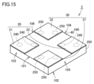
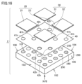
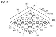
図15は、本発明の実施形態2に係る積層セラミックコンデンサを第1主面側から見た斜視図である。図16は、本発明の実施形態2に係る積層セラミックコンデンサの構成を示す分解斜視図である。図17は、図16の積層セラミックコンデンサをXVII方向から見た斜視図である。図18は、図17の積層セラミックコンデンサをXVIII-XVIII線矢印方向から見た断面図である。図19は、図17の積層セラミックコンデンサをXIX-XIX線矢印方向から見た断面図である。図20は、図17の積層セラミックコンデンサをXX-XX線矢印方向から見た断面図である。
FIG. 15 is a perspective view of a multilayer ceramic capacitor according to
図15~図20に示すように、本発明の実施形態2に係る積層セラミックコンデンサ2は、コンデンサ本体200と、複数の第1ビア導体240と、複数の第2ビア導体250と、複数の第1外部電極20および複数の第2外部電極30と、絶縁層40とを備える。
As shown in Figures 15 to 20, the multilayer
図16~図20に示すように、本発明の実施形態2に係る積層セラミックコンデンサ2は、コンデンサ本体200の内部に設けられた、複数の第1ビア導体240および複数の第2ビア導体250を備える。複数の第1ビア導体240および複数の第2ビア導体250は、行方向および列方向の各々において交互に配置されている。
As shown in Figures 16 to 20, the multilayer
複数の第1ビア導体240の各々は、コンデンサ本体200の第1主面101に露出するとともに第2主面102にも露出している。具体的には、複数の第1ビア導体240の各々は、コンデンサ本体200を上記積層方向に貫通するように設けられている。複数の第1ビア導体240の各々において、上記積層方向の一端は第1主面101と面一に位置しており、他端は第2主面102から突出している。なお、複数の第1ビア導体240の各々の他端は、必ずしも第2主面102から突出していなくてもよく、第2主面102と面一に位置していてもよい。
Each of the multiple first via
複数の第2ビア導体250の各々は、コンデンサ本体200の第1主面101に露出するとともに第2主面102にも露出している。具体的には、複数の第2ビア導体250の各々は、コンデンサ本体200を上記積層方向に貫通するように設けられている。複数の第2ビア導体250の各々において、上記積層方向の一端は第1主面101と面一に位置しており、他端は第2主面102から突出している。なお、複数の第2ビア導体250の各々の他端は、必ずしも第2主面102から突出していなくてもよく、第2主面102と面一に位置していてもよい。
Each of the multiple second via
絶縁層40は、第1主面101上に設けられている。絶縁層40は、第1主面101を全体的に覆っている。絶縁層40は、第1主面101には、複数の第1開口部41hおよび複数の第2開口部42hが形成されている。
The insulating
絶縁層40は、セラミックにより形成することができる。絶縁層40が、セラミックにより形成される場合、絶縁層40を構成する材料として、Al2O3、PZT、SiC、SiO2、およびMgOからなる群から選ばれる少なくとも1種類が用いられる。絶縁層40がセラミックにより形成される場合、積層セラミックコンデンサ2の応力に対する機械的強度を向上させることができる。また、絶縁層40がセラミックにより形成される場合、誘電体層110に含まれるセラミックの粒径と絶縁層40に含まれるセラミックの粒径とを比較したとき、絶縁層40に含まれるセラミックの粒径の方が小さいことが好ましい。
The insulating
絶縁層40をセラミックにより形成する場合、絶縁層40の形成方法としては、エアロゾルデポジション法(AD法)、コールドスプレー法などの溶射法、またはCVD(化学気相蒸着)などを用いてもよい。
When the insulating
また、絶縁層40が、樹脂により形成される場合、絶縁層40を構成する材料は、エポキシ樹脂、シリコーン樹脂、フッ素樹脂、フェノール樹脂、ユリア樹脂、メラミン樹脂、不飽和ポリエステル樹脂、チタン酸バリウム、アルミナ、シリカ、イットリア、およびジルコニアからなる群から選ばれる少なくとも1種類を含み得る。この場合、絶縁層40を構成する材料として、ソルダーレジストとして用いられる金属酸化物を用いた熱硬化性エポキシ樹脂、シリコーン樹脂、フッ素樹脂、フェノール樹脂、メラミン樹脂、チタン酸バリウム、アルミナ、またはシリカなどが好適に用いられる。
In addition, when the insulating
絶縁層40が樹脂により形成される場合は、その形成する手段として、噴霧装置または浸漬装置などを用いることにより、絶縁層40を形成することができる。あるいは、絶縁層40をコンデンサ本体200の第1主面101に貼り付けて形成してもよいし、絶縁層40をスクリーン印刷法により形成してもよい。
When the insulating
上記絶縁材料の物性に応じて、絶縁層40を熱硬化もしくは乾燥させることによって、絶縁層40が積層セラミックコンデンサ2の第1主面101に固着される。
The insulating
図15および図16に示すように、少なくとも1つの第1外部電極20および少なくとも1つの第2外部電極30は、絶縁層40上において互いに間隔をあけて設けられている。本実施形態においては、第1外部電極20は、第1外部電極21および第1外部電極22で構成されている。ただし、第1外部電極20の数は、2つに限られず、1つ以上であればよい。第1外部電極21および第1外部電極22は、矩形状の形状を有し、矩形状の第1主面101における対角線上に位置する角部の上方にそれぞれ位置している。本実施形態においては、第2外部電極30は、第2外部電極31および第2外部電極32で構成されている。ただし、第2外部電極30の数は、2つに限られず、1つ以上であればよい。第2外部電極31および第2外部電極32は、矩形状の形状を有し、矩形状の第1主面101における他の対角線上に位置する角部の上方にそれぞれ位置している。
15 and 16, at least one first
本実施形態においては、第1外部電極21および第1外部電極22の各々は、複数の第1ビア導体240のうちの対応する2つの第1ビア導体240、および、複数の第2ビア導体250うちの2つの第2ビア導体250を覆うように設けられている。ただし、第1外部電極21および第1外部電極22の各々が覆う対応する第1ビア導体240の数は、2つに限られず、3つ以上でもよい。第1外部電極21および第1外部電極22の各々が覆う第2ビア導体250の数は、2つに限られず、1つ以上であればよい。
In this embodiment, each of the first
本実施形態においては、第2外部電極31および第2外部電極32の各々は、複数の第1ビア導体240のうちの2つの第1ビア導体240、および、複数の第2ビア導体250うちの対応する2つの第2ビア導体250を覆うように設けられている。ただし、第2外部電極31および第2外部電極32の各々が覆う第1ビア導体240の数は、2つに限られず、1つ以上であればよい。第2外部電極31および第2外部電極32の各々が覆う対応する第2ビア導体250の数は、2つに限られず、3つ以上でもよい。
In this embodiment, each of the second
第1外部電極21および第1外部電極22の各々は、複数の開口部のうちの対応する2つの第1開口部41hを通じて対応する2つの第1ビア導体240と電気的に接続されている。具体的には、第1外部電極21および第1外部電極22の各々の一部は、第1開口部41h内に設けられて、第1ビア導体240の上記積層方向の一端と接続されている。
Each of the first
図19および図20に示すように、第1外部電極21は、対応する第1内部電極部121と電気的に接続されている2つの第1ビア導体240と電気的に接続されている。同様に、第1外部電極22は、対応する第1内部電極部122と電気的に接続されている2つの第1ビア導体240と電気的に接続されている。ただし、第1外部電極20と第1ビア導体240との接続関係は、上記に限られず、各第1外部電極20に対して、対応する第1内部電極部と電気的に接続されている複数の第1ビア導体240が接続されていればよい。
As shown in Figures 19 and 20, the first
図15、図16、図19および図20に示すように、第2外部電極31および第2外部電極32の各々は、複数の開口部のうちの対応する2つの第2開口部42hを通じて対応する2つの第2ビア導体250と電気的に接続されている。具体的には、第2外部電極31および第2外部電極32の各々の一部は、第2開口部42h内に設けられて、第2ビア導体250の上記積層方向の一端と接続されている。ただし、第2外部電極30と第2ビア導体250との接続関係は、上記に限られず、各第2外部電極30に対して、対応する複数の第2ビア導体250が接続されていればよい。
As shown in Figures 15, 16, 19 and 20, each of the second
本発明の実施形態2に係る積層セラミックコンデンサ2においては、複数の第1ビア導体240および複数の第2ビア導体250は、行方向および列方向の各々において交互に配置されている。これにより、実施形態1に係る積層セラミックコンデンサ1より、積層セラミックコンデンサ2のESLをさらに低くすることができる。
In the multilayer
本発明の実施形態2に係る積層セラミックコンデンサ2においては、複数の第1外部電極20は、複数の開口部のうちの対応する第1開口部41hを通じて対応する複数の第1ビア導体240と電気的に接続されている。少なくとも1つの第2外部電極30は、複数の開口部のうちの対応する第2開口部42hを通じて対応する複数の第2ビア導体250と電気的に接続されている。これにより、第1ビア導体240および第2ビア導体250の配置の影響を抑制して第1外部電極20および第2外部電極30の配置の自由度を確保することができる。すなわち、第1ビア導体240および第2ビア導体250の配置を維持しつつ、第1外部電極20および第2外部電極30を任意の位置に配置しつつ、第1外部電極20と当該第1外部電極20に対応する第1ビア導体240とを電気的に接続し、第2外部電極30と当該第2外部電極30に対応する第2ビア導体250とを電気的に接続することができる。ひいては、汎用的なコンデンサ本体200を用いつつ、第1外部電極20および第2外部電極30の配置の自由度を確保することができる。
In the multilayer
本発明の実施形態2に係る積層セラミックコンデンサ2においては、複数の第1内部電極層120の各々は、同一層内において互いに離間している複数の第1内部電極部で構成されているが、これに限られず、複数の第1内部電極層120の各々は、同一層内において一体で構成されていてもよい。この場合、コンデンサ本体200には、コンデンサ機能部が1つのみ存在する。
In the multilayer
(付記)
上述した例示的な実施形態は、以下の態様の具体例であることが当業者により理解される。
(Additional Note)
It will be appreciated by those skilled in the art that the exemplary embodiments described above are examples of the following aspects.
<1>
誘電体層を挟んで1層ずつ交互に積層方向に積層された複数の第1内部電極層および複数の第2内部電極層を含み、第1主面および該第1主面とは前記積層方向の反対側に位置する第2主面を有するコンデンサ本体と、
前記コンデンサ本体の内部に設けられ、前記複数の第1内部電極層と電気的に接続された複数の第1ビア導体と、
前記コンデンサ本体の内部に設けられ、前記複数の第2内部電極層と電気的に接続された複数の第2ビア導体と、
前記第1主面上に設けられ、複数の開口部が形成された絶縁層と、
前記絶縁層上において互いに間隔をあけて設けられた、少なくとも1つの第1外部電極および少なくとも1つの第2外部電極とを備え、
前記少なくとも1つの第1外部電極は、前記複数の第1ビア導体のうちの対応する複数の第1ビア導体、および、前記複数の第2ビア導体うちの少なくとも1つの第2ビア導体を覆うように設けられており、
前記少なくとも1つの第1外部電極は、前記複数の開口部のうちの対応する開口部を通じて前記対応する複数の第1ビア導体と電気的に接続されており、
前記少なくとも1つの第2外部電極は、前記複数の開口部のうちの対応する開口部を通じて対応する複数の第2ビア導体と電気的に接続されている、積層セラミックコンデンサ。
<1>
a capacitor body including a plurality of first internal electrode layers and a plurality of second internal electrode layers alternately stacked one by one in a stacking direction with a dielectric layer sandwiched therebetween, the capacitor body having a first main surface and a second main surface located on the opposite side of the first main surface in the stacking direction;
a plurality of first via conductors provided inside the capacitor body and electrically connected to the plurality of first internal electrode layers;
a plurality of second via conductors provided inside the capacitor body and electrically connected to the plurality of second internal electrode layers;
an insulating layer provided on the first main surface and having a plurality of openings;
at least one first external electrode and at least one second external electrode provided on the insulating layer and spaced apart from each other;
the at least one first external electrode is provided to cover corresponding ones of the first via conductors and at least one second via conductor of the second via conductors;
the at least one first external electrode is electrically connected to the corresponding first via conductors through a corresponding one of the plurality of openings;
the at least one second external electrode is electrically connected to a corresponding one of the plurality of second via conductors through a corresponding one of the plurality of openings.
<2>
前記少なくとも1つの第2外部電極は、前記複数の第1ビア導体のうちの少なくとも1つの第1ビア導体、および、前記複数の第2ビア導体うちの前記対応する複数の第2ビア導体を覆うように設けられている、<1>に記載の積層セラミックコンデンサ。
<2>
The multilayer ceramic capacitor described in <1>, wherein the at least one second external electrode is arranged to cover at least one first via conductor among the plurality of first via conductors and the corresponding plurality of second via conductors among the plurality of second via conductors.
<3>
前記複数の第1内部電極層の各々は、同一層内において互いに離間している複数の第1内部電極部で構成されており、
前記複数の第2内部電極層の各々は、同一層内において一体で構成されており、
前記複数の第1内部電極部の各々は、前記複数の第1ビア導体のうちの対応する複数の第1ビア導体と電気的に接続されており、
前記少なくとも1つの第1外部電極として、複数の第1外部電極を備え、
前記複数の第1外部電極の各々は、前記複数の第1内部電極部のうちの対応する第1内部電極部と電気的に接続されている複数の第1ビア導体と電気的に接続されている、<1>または<2>に記載の積層セラミックコンデンサ。
<3>
Each of the plurality of first internal electrode layers is composed of a plurality of first internal electrode portions that are spaced apart from each other within the same layer,
Each of the plurality of second internal electrode layers is integrally formed within the same layer,
each of the first internal electrode portions is electrically connected to a corresponding one of the first via conductors;
The at least one first external electrode includes a plurality of first external electrodes,
The multilayer ceramic capacitor described in <1> or <2>, wherein each of the plurality of first external electrodes is electrically connected to a plurality of first via conductors that are electrically connected to a corresponding one of the plurality of first internal electrode portions.
<4>
前記複数の第1ビア導体および前記複数の第2ビア導体の各々は、第2主面側に露出している、<1>から<3>のいずれか1つに記載の積層セラミックコンデンサ。
<4>
The multilayer ceramic capacitor according to any one of <1> to <3>, wherein each of the plurality of first via conductors and the plurality of second via conductors is exposed on a second main surface side.
<5>
前記複数の第1ビア導体は、複数列に並んで配置されており、
前記複数の第2ビア導体は、前記複数の第1ビア導体が並んだ列同士の間で列状に並んで配置されている、<1>から<4>のいずれか1つに記載の積層セラミックコンデンサ。
<5>
The first via conductors are arranged in a plurality of rows,
The multilayer ceramic capacitor according to any one of <1> to <4>, wherein the second via conductors are arranged in rows between the rows of the first via conductors.
<6>
前記複数の第1ビア導体および前記複数の第2ビア導体は、行方向および列方向の各々において交互に配置されている、<1>から<4>のいずれか1つに記載の積層セラミックコンデンサ。
<6>
The multilayer ceramic capacitor according to any one of <1> to <4>, wherein the plurality of first via conductors and the plurality of second via conductors are alternately arranged in both the row direction and the column direction.
上述した実施形態の説明において、組み合わせ可能な構成を相互に組み合わせてもよい。 In the above description of the embodiments, configurations that can be combined may be combined with each other.
今回開示された実施形態はすべての点で例示であって制限的なものではないと考えられるべきである。本発明の範囲は上記した説明ではなくて請求の範囲によって示され、請求の範囲と均等の意味および範囲内でのすべての変更が含まれることが意図される。 The embodiments disclosed herein should be considered in all respects as illustrative and not restrictive. The scope of the present invention is indicated by the claims, not the above description, and is intended to include all modifications within the meaning and scope of the claims.
1,1A,1B,1C,2 積層セラミックコンデンサ、20,20A,21,21A,22,22A 第1外部電極、30,30A,31,32 第2外部電極、40 絶縁層、41h 第1開口部、42h 第2開口部、100,100B,100C,200 コンデンサ本体、101 第1主面、102 第2主面、103 第1側面、104 第2側面、105 第3側面、106 第4側面、110 誘電体層、120 第1内部電極層、120h 第1貫通孔、121,122 第1内部電極部、130 第2内部電極層、130h 第2貫通孔、140,140B,140C,240 第1ビア導体、150,150B,150C,250 第2ビア導体。 1, 1A, 1B, 1C, 2: multilayer ceramic capacitor; 20, 20A, 21, 21A, 22, 22A: first external electrode; 30, 30A, 31, 32: second external electrode; 40: insulating layer; 41h: first opening; 42h: second opening; 100, 100B, 100C, 200: capacitor body; 101: first main surface; 102: second main surface; 103: First side, 104 second side, 105 third side, 106 fourth side, 110 dielectric layer, 120 first internal electrode layer, 120h first through hole, 121, 122 first internal electrode portion, 130 second internal electrode layer, 130h second through hole, 140, 140B, 140C, 240 first via conductor, 150, 150B, 150C, 250 second via conductor.
Claims (6)
前記コンデンサ本体の内部に設けられ、前記複数の第1内部電極層と電気的に接続された複数の第1ビア導体と、
前記コンデンサ本体の内部に設けられ、前記複数の第2内部電極層と電気的に接続された複数の第2ビア導体と、
前記第1主面上に設けられ、複数の開口部が形成された絶縁層と、
前記絶縁層上において互いに間隔をあけて設けられた、少なくとも1つの第1外部電極および少なくとも1つの第2外部電極とを備え、
前記少なくとも1つの第1外部電極は、前記複数の第1ビア導体のうちの対応する複数の第1ビア導体、および、前記複数の第2ビア導体うちの少なくとも1つの第2ビア導体を覆うように設けられており、
前記少なくとも1つの第1外部電極は、前記複数の開口部のうちの対応する開口部を通じて前記対応する複数の第1ビア導体と電気的に接続されており、
前記少なくとも1つの第2外部電極は、前記複数の開口部のうちの対応する開口部を通じて対応する複数の第2ビア導体と電気的に接続されている、積層セラミックコンデンサ。 a capacitor body including a plurality of first internal electrode layers and a plurality of second internal electrode layers alternately stacked one by one in a stacking direction with a dielectric layer sandwiched therebetween, the capacitor body having a first main surface and a second main surface located on the opposite side of the first main surface in the stacking direction;
a plurality of first via conductors provided inside the capacitor body and electrically connected to the plurality of first internal electrode layers;
a plurality of second via conductors provided inside the capacitor body and electrically connected to the plurality of second internal electrode layers;
an insulating layer provided on the first main surface and having a plurality of openings;
at least one first external electrode and at least one second external electrode provided on the insulating layer and spaced apart from each other;
the at least one first external electrode is provided to cover corresponding ones of the first via conductors and at least one second via conductor of the second via conductors;
the at least one first external electrode is electrically connected to the corresponding first via conductors through a corresponding one of the plurality of openings;
the at least one second external electrode is electrically connected to a corresponding one of the plurality of second via conductors through a corresponding one of the plurality of openings.
前記複数の第2内部電極層の各々は、同一層内において一体で構成されており、
前記複数の第1内部電極部の各々は、前記複数の第1ビア導体のうちの対応する複数の第1ビア導体と電気的に接続されており、
前記少なくとも1つの第1外部電極として、複数の第1外部電極を備え、
前記複数の第1外部電極の各々は、前記複数の第1内部電極部のうちの対応する第1内部電極部と電気的に接続されている複数の第1ビア導体と電気的に接続されている、請求項1または請求項2に記載の積層セラミックコンデンサ。 Each of the plurality of first internal electrode layers is composed of a plurality of first internal electrode portions that are spaced apart from each other within the same layer,
Each of the plurality of second internal electrode layers is integrally formed within the same layer,
each of the first internal electrode portions is electrically connected to a corresponding one of the first via conductors;
The at least one first external electrode includes a plurality of first external electrodes,
3. The multilayer ceramic capacitor according to claim 1, wherein each of the plurality of first external electrodes is electrically connected to a plurality of first via conductors which are electrically connected to a corresponding one of the plurality of first internal electrode portions.
前記複数の第2ビア導体は、前記複数の第1ビア導体が並んだ列同士の間で列状に並んで配置されている、請求項1から請求項4のいずれか1項に記載の積層セラミックコンデンサ。 The first via conductors are arranged in a plurality of rows,
5 . The multilayer ceramic capacitor according to claim 1 , wherein the second via conductors are arranged in rows between adjacent rows of the first via conductors.
Priority Applications (3)
| Application Number | Priority Date | Filing Date | Title |
|---|---|---|---|
| JP2025526016A JPWO2024252864A1 (en) | 2023-06-07 | 2024-05-14 | |
| CN202480032157.4A CN121100389A (en) | 2023-06-07 | 2024-05-14 | Laminated ceramic capacitor |
| US19/262,557 US20250336607A1 (en) | 2023-06-07 | 2025-07-08 | Multilayer ceramic capacitor |
Applications Claiming Priority (2)
| Application Number | Priority Date | Filing Date | Title |
|---|---|---|---|
| JP2023093700 | 2023-06-07 | ||
| JP2023-093700 | 2023-06-07 |
Related Child Applications (1)
| Application Number | Title | Priority Date | Filing Date |
|---|---|---|---|
| US19/262,557 Continuation US20250336607A1 (en) | 2023-06-07 | 2025-07-08 | Multilayer ceramic capacitor |
Publications (1)
| Publication Number | Publication Date |
|---|---|
| WO2024252864A1 true WO2024252864A1 (en) | 2024-12-12 |
Family
ID=93795328
Family Applications (1)
| Application Number | Title | Priority Date | Filing Date |
|---|---|---|---|
| PCT/JP2024/017778 Ceased WO2024252864A1 (en) | 2023-06-07 | 2024-05-14 | Multilayer ceramic capacitor |
Country Status (4)
| Country | Link |
|---|---|
| US (1) | US20250336607A1 (en) |
| JP (1) | JPWO2024252864A1 (en) |
| CN (1) | CN121100389A (en) |
| WO (1) | WO2024252864A1 (en) |
Citations (5)
| Publication number | Priority date | Publication date | Assignee | Title |
|---|---|---|---|---|
| JP2004134551A (en) * | 2002-10-10 | 2004-04-30 | Ngk Spark Plug Co Ltd | Multilayer ceramic capacitor and method of manufacturing the same |
| JP2007096258A (en) * | 2005-09-01 | 2007-04-12 | Ngk Spark Plug Co Ltd | Wiring board, ceramic capacitor |
| JP2007096262A (en) * | 2005-09-01 | 2007-04-12 | Ngk Spark Plug Co Ltd | Wiring board, embedded ceramic chip |
| JP2009147178A (en) * | 2007-12-14 | 2009-07-02 | Ngk Spark Plug Co Ltd | Ceramic parts, manufacturing method thereof, wiring board |
| JP2019091877A (en) * | 2017-11-10 | 2019-06-13 | サムソン エレクトロ−メカニックス カンパニーリミテッド. | Multilayer capacitor |
-
2024
- 2024-05-14 CN CN202480032157.4A patent/CN121100389A/en active Pending
- 2024-05-14 WO PCT/JP2024/017778 patent/WO2024252864A1/en not_active Ceased
- 2024-05-14 JP JP2025526016A patent/JPWO2024252864A1/ja active Pending
-
2025
- 2025-07-08 US US19/262,557 patent/US20250336607A1/en active Pending
Patent Citations (5)
| Publication number | Priority date | Publication date | Assignee | Title |
|---|---|---|---|---|
| JP2004134551A (en) * | 2002-10-10 | 2004-04-30 | Ngk Spark Plug Co Ltd | Multilayer ceramic capacitor and method of manufacturing the same |
| JP2007096258A (en) * | 2005-09-01 | 2007-04-12 | Ngk Spark Plug Co Ltd | Wiring board, ceramic capacitor |
| JP2007096262A (en) * | 2005-09-01 | 2007-04-12 | Ngk Spark Plug Co Ltd | Wiring board, embedded ceramic chip |
| JP2009147178A (en) * | 2007-12-14 | 2009-07-02 | Ngk Spark Plug Co Ltd | Ceramic parts, manufacturing method thereof, wiring board |
| JP2019091877A (en) * | 2017-11-10 | 2019-06-13 | サムソン エレクトロ−メカニックス カンパニーリミテッド. | Multilayer capacitor |
Also Published As
| Publication number | Publication date |
|---|---|
| JPWO2024252864A1 (en) | 2024-12-12 |
| CN121100389A (en) | 2025-12-09 |
| US20250336607A1 (en) | 2025-10-30 |
Similar Documents
| Publication | Publication Date | Title |
|---|---|---|
| US10026556B2 (en) | Electronic component | |
| US9892855B2 (en) | Electronic component | |
| CN105869833A (en) | Electronic component and board having the same | |
| US20150287514A1 (en) | Chip coil component and board for mounting the same | |
| CN109935467B (en) | Capacitor assembly | |
| US11335505B2 (en) | Electronic component | |
| US11417465B2 (en) | Electronic component having a plurality of internal electrodes | |
| US10614946B2 (en) | Electronic component | |
| JP2022067931A (en) | Electronic component | |
| KR20190121208A (en) | Multilayer ceramic electronic component and interposer included therein | |
| US10755861B2 (en) | Electronic component | |
| CN114023567A (en) | Multilayer capacitor and board having the same mounted thereon | |
| US11437189B2 (en) | Electronic component having plurality of internal electrodes | |
| JP2010514169A (en) | Electrical components, as well as the outer contacts of electrical components | |
| US12308173B2 (en) | Ceramic electronic component including insulating layer | |
| JP5437248B2 (en) | Electrical multilayer components | |
| CN111326344B (en) | Multilayer ceramic electronic component and circuit board | |
| WO2024252864A1 (en) | Multilayer ceramic capacitor | |
| WO2024252863A1 (en) | Multilayer ceramic capacitor | |
| JP7230517B2 (en) | electronic components | |
| CN112530699A (en) | Multilayer capacitor | |
| JP6115276B2 (en) | Multilayer capacitor | |
| JP4412386B2 (en) | Feed-through multilayer capacitor | |
| JP2018098701A (en) | Balance-unbalance converter | |
| CN114823143B (en) | Multilayer capacitor |
Legal Events
| Date | Code | Title | Description |
|---|---|---|---|
| 121 | Ep: the epo has been informed by wipo that ep was designated in this application |
Ref document number: 24819101 Country of ref document: EP Kind code of ref document: A1 |
|
| ENP | Entry into the national phase |
Ref document number: 2025526016 Country of ref document: JP Kind code of ref document: A |
|
| WWE | Wipo information: entry into national phase |
Ref document number: 2025526016 Country of ref document: JP |
|
| NENP | Non-entry into the national phase |
Ref country code: DE |