WO2024252865A1 - パターン検査装置及びパターン検査方法 - Google Patents
パターン検査装置及びパターン検査方法 Download PDFInfo
- Publication number
- WO2024252865A1 WO2024252865A1 PCT/JP2024/017787 JP2024017787W WO2024252865A1 WO 2024252865 A1 WO2024252865 A1 WO 2024252865A1 JP 2024017787 W JP2024017787 W JP 2024017787W WO 2024252865 A1 WO2024252865 A1 WO 2024252865A1
- Authority
- WO
- WIPO (PCT)
- Prior art keywords
- reference image
- filter function
- range
- parameters
- circuit
- Prior art date
- Legal status (The legal status is an assumption and is not a legal conclusion. Google has not performed a legal analysis and makes no representation as to the accuracy of the status listed.)
- Ceased
Links
Images


Classifications
-
- G—PHYSICS
- G01—MEASURING; TESTING
- G01N—INVESTIGATING OR ANALYSING MATERIALS BY DETERMINING THEIR CHEMICAL OR PHYSICAL PROPERTIES
- G01N21/00—Investigating or analysing materials by the use of optical means, i.e. using sub-millimetre waves, infrared, visible or ultraviolet light
- G01N21/84—Systems specially adapted for particular applications
- G01N21/88—Investigating the presence of flaws or contamination
- G01N21/8851—Scan or image signal processing specially adapted therefor, e.g. for scan signal adjustment, for detecting different kinds of defects, for compensating for structures, markings, edges
-
- G—PHYSICS
- G01—MEASURING; TESTING
- G01N—INVESTIGATING OR ANALYSING MATERIALS BY DETERMINING THEIR CHEMICAL OR PHYSICAL PROPERTIES
- G01N21/00—Investigating or analysing materials by the use of optical means, i.e. using sub-millimetre waves, infrared, visible or ultraviolet light
- G01N21/84—Systems specially adapted for particular applications
- G01N21/88—Investigating the presence of flaws or contamination
- G01N21/95—Investigating the presence of flaws or contamination characterised by the material or shape of the object to be examined
- G01N21/956—Inspecting patterns on the surface of objects
- G01N21/95607—Inspecting patterns on the surface of objects using a comparative method
-
- G—PHYSICS
- G03—PHOTOGRAPHY; CINEMATOGRAPHY; ANALOGOUS TECHNIQUES USING WAVES OTHER THAN OPTICAL WAVES; ELECTROGRAPHY; HOLOGRAPHY
- G03F—PHOTOMECHANICAL PRODUCTION OF TEXTURED OR PATTERNED SURFACES, e.g. FOR PRINTING, FOR PROCESSING OF SEMICONDUCTOR DEVICES; MATERIALS THEREFOR; ORIGINALS THEREFOR; APPARATUS SPECIALLY ADAPTED THEREFOR
- G03F1/00—Originals for photomechanical production of textured or patterned surfaces, e.g., masks, photo-masks, reticles; Mask blanks or pellicles therefor; Containers specially adapted therefor; Preparation thereof
- G03F1/68—Preparation processes not covered by groups G03F1/20 - G03F1/50
- G03F1/82—Auxiliary processes, e.g. cleaning or inspecting
- G03F1/84—Inspecting
-
- G—PHYSICS
- G03—PHOTOGRAPHY; CINEMATOGRAPHY; ANALOGOUS TECHNIQUES USING WAVES OTHER THAN OPTICAL WAVES; ELECTROGRAPHY; HOLOGRAPHY
- G03F—PHOTOMECHANICAL PRODUCTION OF TEXTURED OR PATTERNED SURFACES, e.g. FOR PRINTING, FOR PROCESSING OF SEMICONDUCTOR DEVICES; MATERIALS THEREFOR; ORIGINALS THEREFOR; APPARATUS SPECIALLY ADAPTED THEREFOR
- G03F7/00—Photomechanical, e.g. photolithographic, production of textured or patterned surfaces, e.g. printing surfaces; Materials therefor, e.g. comprising photoresists; Apparatus specially adapted therefor
- G03F7/20—Exposure; Apparatus therefor
-
- G—PHYSICS
- G06—COMPUTING OR CALCULATING; COUNTING
- G06T—IMAGE DATA PROCESSING OR GENERATION, IN GENERAL
- G06T7/00—Image analysis
- G06T7/0002—Inspection of images, e.g. flaw detection
- G06T7/0004—Industrial image inspection
- G06T7/001—Industrial image inspection using an image reference approach
-
- G—PHYSICS
- G06—COMPUTING OR CALCULATING; COUNTING
- G06T—IMAGE DATA PROCESSING OR GENERATION, IN GENERAL
- G06T2207/00—Indexing scheme for image analysis or image enhancement
- G06T2207/20—Special algorithmic details
- G06T2207/20024—Filtering details
-
- G—PHYSICS
- G06—COMPUTING OR CALCULATING; COUNTING
- G06T—IMAGE DATA PROCESSING OR GENERATION, IN GENERAL
- G06T2207/00—Indexing scheme for image analysis or image enhancement
- G06T2207/30—Subject of image; Context of image processing
- G06T2207/30108—Industrial image inspection
- G06T2207/30148—Semiconductor; IC; Wafer
Definitions
- JP2023-095655 application number filed in Japan on June 9, 2023. All contents of JP2023-095655 are incorporated herein by reference.
- One aspect of the present invention relates to a pattern inspection device and a pattern inspection method.
- the present invention relates to a pattern inspection technique for inspecting pattern defects of an object that serves as a sample for use in semiconductor manufacturing, and to a method for inspecting defects in a mask used when manufacturing semiconductor elements.
- a known inspection method is to compare an optical image of a pattern formed on a sample such as a lithography mask captured at a specified magnification using a magnifying optical system with design data.
- a sample such as a lithography mask captured at a specified magnification using a magnifying optical system
- design data For example, there is a "die to database inspection" in which the pattern design CAD data is converted into a device input format for input by a drawing device when drawing the pattern on the mask, and the drawing data (design pattern data) is input to an inspection device, a design image (reference image) is generated based on this, and this is compared with an optical image of the pattern, which is the measurement data.
- the sample is placed on a stage, and the stage moves so that a light beam scans the sample, and the inspection is performed.
- the light beam is irradiated onto the sample by a light source and an illumination optical system.
- the light transmitted through or reflected from the sample is imaged on a sensor via the optical system.
- the image captured by the sensor is sent to a comparison circuit as measurement data.
- the comparison circuit after aligning the images, the measurement data and reference data are compared according to an appropriate algorithm, and if they do not match, it is determined that there is a pattern defect.
- the pixel data of the optical image captured from the sample is in a filtered state due to the resolution characteristics of the optical system used for capturing the image, in other words, it is in an analog state that changes continuously, so the image intensity (shade value) differs from the design image, which is a digital value. For this reason, the design image is filtered to create a reference image that is close to the measurement image, and then a comparison process is performed.
- one aspect of the present invention provides an inspection device and method that can shorten the processing time required to obtain a filter function suitable for the current inspection.
- a pattern inspection apparatus comprises: an optical image acquisition mechanism for acquiring an optical image of the pattern-formed sample to be inspected; a parameter range setting circuit for setting a range of a reference image generating parameter according to a degree of agreement with a past inspection condition parameter; a filter function generating circuit that generates a plurality of filter function candidates using values within the range of the set reference image generating parameters; a decision circuit for deciding a filter function for generating a reference image from among the plurality of generated filter function candidates; a reference image generating circuit for generating a reference image by using the determined filter function; a comparison circuit for comparing the optical image with a reference image;
- the present invention is characterized by comprising:
- a pattern inspection method includes: Acquiring an optical image of the patterned specimen; Set a range of reference image generation parameters according to the degree of agreement with past inspection condition parameters; generating a plurality of filter function candidates using values within the range of the set reference image generation parameters; determining a filter function for generating a reference image from among the plurality of generated filter function candidates; Creating a reference image using the determined filter function; comparing the optical image with the reference image and outputting the result; It is characterized by:
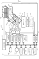
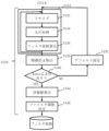
- FIG. 1 is a configuration diagram showing a configuration of a pattern inspection device according to a first embodiment
- FIG. 2 is a conceptual diagram for explaining an inspection area in the first embodiment
- 2 is a block diagram showing an example of an internal configuration of a filter function calculation circuit according to the first embodiment.
- FIG. FIG. 2 is a flowchart showing main steps of the pattern inspection method according to the first embodiment.
- 1 is a diagram showing an example of inspection condition parameters and the weighting of each parameter in the first embodiment
- 13 illustrates an example of the relationship between the degree of match and the ratio of narrowing the range in the first embodiment.
- 13 is a diagram showing an example of the relationship between reference image generating parameters, filter functions, scores, and rankings in a past inspection in embodiment 1.
- FIG. 11A and 11B are diagrams showing an example of a reference image generation parameter range and a set result in the first embodiment.
- FIG. 4 is a diagram showing an example of an internal process of a filter function generating process in the first embodiment.
- 1A to 1C are diagrams showing examples of graphic patterns before and after resizing in the first embodiment.
- 5A to 5C are diagrams showing examples of figure patterns before and after rounding processing in the first embodiment.
- 5A to 5C are diagrams for explaining an example of a relationship between a filter function, a design image, and a measurement image in the first embodiment.
- 5 is a diagram for explaining an example of a method for calculating coefficients of a filter function in the first embodiment.
- Fig. 1 is a configuration diagram showing the configuration of a pattern inspection apparatus in embodiment 1.
- an inspection apparatus 100 for inspecting a sample for example, a pattern formed on a mask, includes an optical image acquisition mechanism 150 and a control system circuit 160 (control unit).
- the optical image acquisition mechanism 150 has a light source 103, an illumination optical system 170, a movably arranged XY ⁇ table 102, a magnifying optical system 104, an image sensor 105 (an example of a sensor), a sensor circuit 106, a stripe pattern memory 123, and a laser length measurement system 122.
- a sample 101 is arranged on the XY ⁇ table 102.
- the sample 101 includes, for example, a photomask for exposure that transfers a pattern onto a wafer.
- this photomask has a pattern formed thereon that is made up of a plurality of geometric patterns to be inspected.
- the sample 101 is arranged on the XY ⁇ table 102 with, for example, the pattern-forming surface facing downwards.
- a line sensor or a two-dimensional sensor is used as the imaging sensor 105.
- a TDI (time delay integration) sensor has multiple photosensor elements arranged two-dimensionally. A predetermined image accumulation time is set for each photosensor element when capturing an image.
- the output of multiple photosensor elements lined up in the scanning direction is integrated and output. Multiple photosensor elements lined up in the scanning direction capture the same pixel while shifting the time in accordance with the movement of the XY ⁇ table 102.
- a line sensor is used, multiple photosensor elements are arranged so that they are lined up in a direction perpendicular to the scanning direction.
- control computer 110 is connected to the position circuit 107, comparison circuit 108, expansion circuit 111, reference circuit 112, autoloader control circuit 113, table control circuit 114, filter function calculation circuit 140, magnetic disk device 109, memory 116, flexible disk device (FD) 115, CRT 117, pattern monitor 118, and printer 119 via a bus 120.
- the sensor circuit 106 is connected to a stripe pattern memory 123, which is connected to the comparison circuit 108.
- the XY ⁇ table 102 is driven by an X-axis motor, a Y-axis motor, and a ⁇ -axis motor.
- the XY ⁇ table 102 is an example of a stage.
- the series of "circuits” such as the position circuit 107, comparison circuit 108, expansion circuit 111, reference circuit 112, autoloader control circuit 113, table control circuit 114, and filter function calculation circuit 140 have a processing circuit.
- processing circuits include electric circuits, computers, processors, circuit boards, quantum circuits, or semiconductor devices. Each circuit may be configured using the same processing circuit (one processing circuit), or different processing circuits (separate processing circuits).
- the series of "circuits” such as the position circuit 107, comparison circuit 108, expansion circuit 111, reference circuit 112, autoloader control circuit 113, table control circuit 114, and filter function calculation circuit 140 may be configured and executed by the control computer 110.
- Input data or calculation results required for the position circuit 107, comparison circuit 108, expansion circuit 111, reference circuit 112, autoloader control circuit 113, table control circuit 114, and filter function calculation circuit 140 are stored in a memory (not shown) in each circuit or in memory 116.
- Input data or calculation results required for the control computer 110 are stored in a memory (not shown) in the control computer 110 or in memory 116.
- Programs for executing the processors, etc. may be recorded on recording media such as the magnetic disk device 109, FD 115, or ROM (read only memory).
- a high-magnification inspection optical system is composed of the light source 103, the XY ⁇ table 102, the illumination optical system 170, the magnifying optical system 104, the image sensor 105, and the sensor circuit 106.
- the XY ⁇ table 102 is driven by the table control circuit 114 under the control of the control computer 110. It can be moved by a drive system such as a three-axis (X-Y- ⁇ ) motor that drives in the X, Y, and ⁇ directions. These X, Y, and ⁇ motors can be, for example, step motors.
- the XY ⁇ table 102 can be moved in the horizontal and rotational directions by the motors of the X, Y, and ⁇ axes.
- the sample 101 is transported onto the XY ⁇ table 102 from the autoloader 130 controlled by the autoloader control circuit 113.
- the moving position of the sample 101 placed on the XY ⁇ table 102 is measured by the laser length measurement system 122 and supplied to the position circuit 107.
- Drawing data (design data) that is the basis for forming a pattern on the sample 101 to be inspected is input from outside the inspection device 100 and stored in the magnetic disk device 109.
- the drawing data defines multiple geometric patterns, and each geometric pattern is usually composed of a combination of multiple element geometric patterns. However, a geometric pattern composed of a single geometric figure may also exist.
- FIG. 1 shows the components necessary for explaining the first embodiment. It goes without saying that the inspection device 100 may also include other components that are normally required.
- FIG. 2 is a conceptual diagram for explaining the inspection area in the first embodiment.
- the inspection area 10 (whole inspection area) of the sample 101 is virtually divided into a plurality of rectangular inspection stripes 20 having a scan width W of the image sensor 105, for example, in the Y direction.
- the inspection device 100 then acquires an image (stripe area image) for each inspection stripe 20.
- an image of the figure pattern arranged within the inspection stripe 20 is captured in the longitudinal direction (X direction) of the stripe area using laser light (inspection light).
- the inspection stripes 20 are set so that adjacent inspection stripes 20 overlap with each other by a predetermined margin width.
- the movement of the XY ⁇ table 102 causes the image sensor 105 to move continuously in the X direction relative to the object, acquiring an optical image.
- the image sensor 105 continuously captures optical images of a scan width W as shown in FIG. 2.
- the image sensor 105 moves in the Y direction to the position of the next inspection stripe 20, and then moves in the reverse direction while similarly capturing optical images of the scan width W continuously.
- imaging is repeated in the forward (FWD)-backward (BWD) directions, which go in opposite directions on the outbound and return journeys.
- the stripe area image of each inspection stripe 20 is divided into a number of rectangular frame area 30 images (frame images 31) as shown in FIG. 2. Then, inspection is carried out for each frame image 31 of the frame area 30. For example, it is divided into a size of 512 x 512 pixels. Therefore, a reference image to be compared with the frame images 31 of the frame area 30 is also created for each frame area 30.
- the imaging direction is not limited to repeated forward (FWD)-backward (BWD). Imaging may be performed from one direction. For example, FWD-FWD may be repeated. Or BWD-BWD may be repeated.
- FWD-FWD may be repeated.
- BWD-BWD may be repeated.
- the pixel data of the optical image captured from the sample 101 is in a filtered state due to the resolution characteristics of the optical system used for capturing the image, in other words, in a continuously changing analog state, so the image intensity (shade value) differs from the design image, described below, which has a digital value. Therefore, the design image is filtered to bring it closer to the measurement data before comparison processing is performed.
- a filter function for performing such filtering is first calculated prior to performing the inspection processing of the sample 101.
- FIG. 3 is a block diagram showing an example of the internal configuration of a filter function calculation circuit in the first embodiment.
- the filter function calculation circuit 140 includes storage devices 61, 70, 71, 73, and 75 such as magnetic disks, a coincidence calculation unit 60, a parameter range setting unit 62, a filter function generation unit 64, a frame image creation unit 72, a tone difference calculation unit 80, a judgment unit 82, a decision unit 84, and an evaluation value calculation unit 86.
- the filter function generation unit 64 also includes a resizing unit 66, a rounding unit 67, and a filter coefficient calculation unit 68.
- a series of " ⁇ units” such as the coincidence calculation unit 60, parameter range setting unit 62, filter function generation unit 64 (resizing processing unit 66, rounding processing unit 67, and filter coefficient calculation unit 68), frame image creation unit 72, tone difference calculation unit 80, judgment unit 82, decision unit 84, and evaluation value calculation unit 86 have processing circuits.
- processing circuits include electric circuits, computers, processors, circuit boards, quantum circuits, or semiconductor devices.
- each " ⁇ unit” may use a common processing circuit (the same processing circuit). Alternatively, they may use different processing circuits (separate processing circuits).
- the input data or the calculated results required for the coincidence calculation unit 60, parameter range setting unit 62, filter function generation unit 64 (resizing unit 66, rounding unit 67, and filter coefficient calculation unit 68), frame image creation unit 72, tone difference calculation unit 80, judgment unit 82, decision unit 84, and evaluation value calculation unit 86 are stored in a memory (not shown) in the filter function calculation circuit 140 or in memory 116 each time.
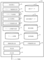
- FIG. 4 is a flow chart showing the main steps of the pattern inspection method in the first embodiment.
- the pattern inspection method in the first embodiment performs a series of steps including a coincidence calculation step (S102), a parameter range setting step (S104), a representative frame selection step (S110), a stripe image acquisition step (S114), a representative frame image creation step (S116), a representative design image creation step (S118), a filter function calculation step (S130), a stripe image acquisition step (S202), a frame image creation step (S204), a design image creation step (S212), a reference image creation step (S214), and a comparison step (S230).
- a coincidence calculation step S102
- S104 parameter range setting step
- S110 a representative frame selection step
- S114 stripe image acquisition step
- S116 representative frame image creation step
- S118 representative design image creation step
- S130 filter function calculation step
- S202 stripe image acquisition step
- S204 frame image creation step
- S212 design image creation step
- S214 reference
- the coincidence calculation unit 60 inputs the test condition parameters for the test and calculates the coincidence with the test condition parameters for a previously performed test.
- Fig. 5 is a diagram showing an example of inspection condition parameters and the weighting of each parameter in the first embodiment.
- the inspection condition parameters in the first embodiment include, for example, pattern condition parameters and imaging condition parameters.
- the pattern condition parameters include, for example, a mask series name, a mask layer name, a mask layout name, a film type, etc.
- the imaging condition parameters include, for example, a stage speed, an inspection sensitivity (S), etc. 5 shows a case where the weighting of the mask series name is 1, the weighting of the mask layer name is 2, the weighting of the mask layout name is 5, the weighting of the film type is 1, the weighting of the stage speed is 1, and the weighting of the inspection sensitivity (threshold) is 2.
- the weighting values may be set based on experience or the like.
- the parameters of the pattern conditions are defined, for example, as additional information of the drawing data. Alternatively, it is also suitable to obtain them by capturing an ID image (not shown) formed outside the inspection area 10 of the sample 101.
- the additional information or ID image defines, for example, the identification number of the mask that will become the sample 101, the mask series name, the mask layer name, the mask layout name, the film type, etc.
- the mask series name for example, a name indicating a leading-edge mask, or a name of a mask on which a pattern of a rough pattern size is formed, or other names according to the generation of the mask to be manufactured, are used.
- the mask layer name for example, the name of a layer in the multilayer wiring layer of the semiconductor device is used.
- the mask layout name for example, a name identifying the circuit of the semiconductor device is used.
- the film type for example, a name indicating the type of film used to form the pattern of the mask that will become the sample 101 is used.
- the coincidence calculation unit 60 calculates the coincidence using at least one of the parameters of the pattern conditions and the parameters of the imaging conditions. Here, a case where the calculation is performed using both will be described.
- the inspection condition parameters of the past inspections are stored in the storage device 61 for each sample that was previously inspected.
- the coincidence is defined by the following relational expression (1) using the weights of each parameter of the inspection condition parameters.
- Degree of agreement sum of weights of matched parameters / sum of weights of all parameters
- the sample with the highest degree of match is stored in the storage device 61, it is preferable to use the sample with the highest degree of match as the previously tested sample. Alternatively, a preset number or percentage of samples may be selected in order of degree of match, starting from the sample with the highest degree of match.
- the parameter range setting unit 62 changes and sets the range of the target reference image generation parameters according to the degree of agreement with past inspection condition parameters in order to determine the reference image generation parameters used for reference image generation.
- the reference image generation parameters include at least one of the resizing amount and the corner rounding amount.
- the range of the target reference image generation parameters is changed from a preset default range.
- the range of the target reference image generation parameters is set to a range narrower than the preset default range.
- the parameter range setting unit 62 inputs the inspection condition parameters of the inspection, and changes and sets multiple values used for reference image generation of at least one of the reference image generation parameters of the resizing amount and the corner rounding amount to a range narrower than the preset default range of the reference image generation parameters according to the degree of agreement with the inspection condition parameters implemented in the past.
- FIG. 6 shows an example of the relationship between the degree of match and the ratio of narrowing the range in embodiment 1.
- the degree of match is 0 (0%) or more and less than 0.2 (20%), 100% of the default reference image generation parameter range is used.
- the degree of match is 0.2 (20%) or more and less than 0.4 (40%), 80% of the default reference image generation parameter range is used.
- the degree of match is 0.4 (80%) or more and less than 0.6 (60%), 60% of the default reference image generation parameter range is used.
- the degree of match is 0.6 (80%) or more and less than 0.8 (80%)
- 40% of the default reference image generation parameter range is used.
- the degree of match is 0.8 (80%) or more and less than 1 (100%), 20% of the default reference image generation parameter range is used. Note that if the degree of match is 1 (100%), 20% of the default reference image generation parameter range may be used, or the past reference image generation parameters that matched may be used as is. Alternatively, a preset percentage within the default reference image generation parameter range of 0-20% may be used.
- a threshold value Tth may be set in advance for the degree of match, and the parameter range setting unit 62 may set a default range for the reference image generation parameters when the calculated degree of match is less than the threshold value Tth.
- the degree of match is less than the threshold value Tth, it is also preferable to use 100% of the default reference image generation parameter range.
- the example in FIG. 6 indicates that, for example, when the degree of match is less than 0.6, 100% of the default reference image generation parameter range is used.
- the percentage of the default reference image generation parameter range that will be used is set as follows:
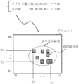
- FIG. 7 is a diagram showing an example of the relationship between the reference image generating parameters, the filter functions, the scores, and the rankings in the past inspections in the first embodiment.
- the reference image generating parameters include the resize amount and the rounding amount.
- a case where the range of A1 to An is set as the default resize amount range is shown.
- a case where the range of B1 to Bm is set as the default rounding amount range is shown.
- Such a range may be determined by empirical rules or the like.
- a plurality of resize amounts A1, A2, A3, ..., An at preset intervals within the resize amount range are used.
- a plurality of rounding amounts B1, B2, B3, ..., Bm at preset intervals within the rounding amount range are used.
- filter functions a1, a2, a3, . . . are generated for all combinations of a plurality of resizing amounts A1, A2, A3, .
- the evaluation value of the generated filter function is calculated as a score value for each combination.
- the evaluation value for example, it is preferable to use the sum of squares of the gradation difference for each pixel between the reference image created using the generated filter function and the corresponding measurement image (optical image) or the square root of the sum of squares of the difference.
- the maximum gradation difference for each pixel between the reference image created using the generated filter function and the corresponding measurement image (optical image).
- the example of FIG. 7 shows a case where the square root of the sum of squares of the difference is used. Then, for each combination, the ranking is recorded in ascending order of score.
- a list of the relationships between the reference image generating parameters, filter functions, scores, and rankings is created for each past inspection, and is stored as past data in the storage device 61 in association with the sample to be inspected.
- the range of reference image generation parameters or the number of values used is changed or narrowed down. Specifically, the range of parameter values used for at least one of the default range of the resizing amount and the default range of the rounding amount is changed. Specifically, it operates as follows.
- the parameter range setting unit 62 sets combinations with a ratio according to the degree of matching from the top ranking combinations based on the data from past inspections. For example, if the degree of matching is 0.9, combinations of resizing and rounding amounts within a range narrowed down to the top 20% are extracted, and the extracted combinations of resizing and rounding amounts are set.
- FIG. 8 is a diagram showing an example of the reference image generation parameter range and the set result in the first embodiment.
- the vertical axis indicates the rounding amount
- the horizontal axis indicates the resizing amount.
- A1 to An which is the default resizing amount range
- n resizing amount values there are n resizing amount values.
- B1 to Bm which is the default rounding amount range
- m rounding amount values there are m rounding amount values.
- the default range may be set according to empirical rules. Therefore, there are (m ⁇ n) combinations of resizing amount and rounding amount.
- N% combinations according to the degree of matching are extracted in order from the smallest score, so that the number of combinations used to generate a filter function can be narrowed down below the number of combinations in the default range.
- the example of FIG. 8 shows an example of a number of narrowed down combinations.
- a representative frame to be used for determining a filter function during inspection of the sample 101 is selected.
- the stripe region of each inspection stripe 20 is divided into, for example, a plurality of frame regions 30, and inspection is performed for each frame region 30.
- the inspection region 10 of the sample 101 is virtually divided into a plurality of frame regions 30, and inspection is performed for each frame region 30.
- a frame region (representative frame 32) to be used for generating a filter function is selected from the inspection region 10 of the sample 101.
- the position of the selected frame region (representative frame 32) may be arbitrarily set in advance by the user. Then, the position of the selected frame region may be set in the control computer 110. Alternatively, a predetermined selection condition may be set, and the control computer 110 may select the position of the frame region.
- the optical image acquisition mechanism 150 acquires an optical image of the inspection stripe 20 including the representative frame 32 of the photomask that is the sample 101. Specifically, it operates as follows.
- the XY ⁇ table 102 is moved to a position where the inspection stripe 20 including the representative frame 32 can be imaged.
- a laser light e.g., DUV light
- DUV light with a wavelength below the ultraviolet range, which serves as inspection light
- the light transmitted through the sample 101 passes through a magnifying optical system 104 and is focused as an optical image on an imaging sensor 105 (an example of a sensor), where it is incident.
- the pattern image formed on the image sensor 105 is photoelectrically converted by each light receiving element of the image sensor 105, and then A/D (analog-to-digital) converted by the sensor circuit 106.
- the pixel data of the inspection stripe 20 to be measured is then stored in the stripe pattern memory 123.
- the stripe area image is then sent to the filter function calculation circuit 140 together with data indicating the position of the sample 101 on the XY ⁇ table 102 output from the position circuit 107.
- the measurement data (pixel data) is, for example, 8-bit unsigned data, and represents the brightness gradation (amount of light) of each pixel.
- the stripe area image output to the filter function calculation circuit 140 is stored in the storage device 71.
- the frame image creation unit 72 creates a frame image (representative frame image) of the representative frame 32.
- the stripe area image is divided in the x direction at a predetermined size so as to extract the frame image (representative frame image) of the representative frame 32 from the stripe area image (optical image) of the inspection stripe 20 that includes the representative frame 32.
- it is divided into frame images of 512 x 512 pixels.
- Data of the divided representative frame images is output to and stored in the storage device 73.
- the expansion circuit 111 creates a design image (representative design image) by expanding an image based on the design pattern data that is the basis for pattern formation of the inspected sample 101.
- the design data is read from the magnetic disk device 109 through the control computer 110, and each graphic pattern in the area of the representative frame 32 defined in the read design data is converted into binary or multi-value image data (image expansion) to create the design image (representative design image).
- the figures defined in the design pattern data are, for example, rectangles and triangles as basic figures, and graphic data (vector data) is stored that defines the shape, size, position, etc. of each pattern figure using information such as the coordinates (x, y) at the reference position of the figure, the length of the sides, and a figure code that serves as an identifier to distinguish the type of figure, such as a rectangle or triangle.
- the expansion circuit 111 When the information of the design pattern that becomes such graphic data is input to the expansion circuit 111, it is expanded to data for each graphic, and graphic codes and dimensions indicating the graphic shapes of the graphic data are interpreted. Then, binary or multi-value design image data is expanded as a pattern arranged in a grid with a predetermined quantization dimension as a unit, and output.
- the design data is read, the inspection area is virtually divided into grids with a predetermined dimension as a unit, the occupancy rate of the graphic in the design pattern is calculated for each grid, and n-bit occupancy data is output. For example, it is preferable to set one grid as one pixel.
- the filter function calculation circuit 140 calculates a filter function for creating a reference image. Specifically, it operates as follows.
- FIG. 9 is a diagram showing an example of the internal steps of the filter function generation step in the first embodiment.
- the filter function calculation step (S130) performs a series of steps as its internal steps, namely, a filter function generation step (S131), a tone difference calculation step (S138), a judgment step (S140), a default setting step (S142), an evaluation value calculation step (S144), and a filter function determination step (S146).
- the temporary filter function generation step (S131) performs a resizing step (S132), a rounding process step (S134), and a filter coefficient calculation step (S136) as its internal steps.
- the filter function generation unit 64 In the filter function generation step (S131), the filter function generation unit 64 generates a filter function for creating a reference image using a value within the range of the set reference image generation parameters. Specifically, the filter function generation unit 64 generates a plurality of filter function candidates for creating a reference image using each of a plurality of values within the changed or narrowed down range of the reference image generation parameters. Specifically, a filter function candidate is generated for each of a plurality of narrowed down combinations of resizing amount and rounding amount. A more detailed explanation is given below.
- the resizing processing unit 66 resizes the graphic pattern in the design image of the representative frame 32 using one of a plurality of values within the range of the changed or narrowed-down reference image generation parameters. Specifically, the graphic pattern in the design image of the representative frame 32 is resized for each of the narrowed-down combinations of resizing amount and rounding amount.
- FIG. 10 is a diagram showing an example of a figure pattern before and after resizing in the first embodiment.
- the example of FIG. 10 shows a figure pattern 14 in which the width size of the figure pattern 12 in the design image is resized by a resize amount A'.
- the default range of the resize amount is, for example, from -5 pixels to +5 pixels, it is changed and set or narrowed down to, for example, seven values of 0.5 pixels each in the range of -1 pixel to +2 pixels (-1 pixel, -0.5 pixel, 0, +0.5 pixel, +1 pixel, +1.5 pixel, +2 pixels).
- a negative value indicates that the width size is resized in a direction that reduces the width size.
- a positive value indicates that the width size is resized in a direction that increases the width size. Also, for example, 0.5 pixels indicates that the resize amount is 1/2 the pixel size.
- the example of FIG. 10 shows a case where the width size of the figure pattern 12 is resized in a direction that reduces the width size.
- the example of FIG. 10 shows an example where the width size in the x direction is resized, but the width size in the y direction may be resized instead of the width size in the x direction. Alternatively, both the width size in the x direction and the width size in the y direction may be resized.
- the rounding processor 67 rounds the corners of the geometric pattern in the design image of the representative frame 32 using one of a plurality of values within the range of the changed or narrowed-down reference image generation parameters. Specifically, for each of the plurality of narrowed-down combinations of resize amount and rounding amount, the rounding processor 67 rounds the corners of the geometric pattern in the design image of the representative frame 32. It is preferable to perform the rounding process on the geometric pattern after resizing.
- FIG. 11 shows an example of a graphic pattern before and after rounding in the first embodiment.
- the example in FIG. 11 shows a graphic pattern 16 in which the corners of a resized graphic pattern 14 have been rounded by a rounding amount B'.
- the default range of the rounding amount is, for example, from 0 to +2 pixels, it is changed or narrowed down to, for example, five values of 0.2 pixels each in the range from 0.2 pixels to 1 pixel (0.2 pixels, 0.4 pixels, 0.6 pixels, 0.8 pixels, 1 pixel).
- 0.2 pixels indicates a rounding amount of 1/5 the pixel size.
- the rounding amount indicates the radius of curvature. In the example in FIG. 11, the upper left corner is shown, but the other corners are rounded in the same manner.
- the filter coefficient calculation unit 68 calculates the coefficients of a filter function using a design image that has been resized and/or rounded using one of a plurality of values within the range of the changed or narrowed-down reference image generation parameters. Specifically, for each of the plurality of narrowed-down combinations of resize amount and round amount, the filter function coefficients are calculated using a design image that has been resized and/or rounded.
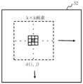
- FIG. 12 is a diagram for explaining an example of the relationship between the filter function, the design image, and the measurement image in the first embodiment.
- FIG. 13 is a diagram for explaining an example of a method for calculating coefficients of a filter function in the first embodiment.
- an unknown coefficient matrix a(i,j) (an example of a filter function) consisting of k ⁇ k elements, which is less than the number of pixels in the frame region, is obtained by the following method.
- a 15 ⁇ 15 coefficient matrix a(i,j) is obtained for an image of a frame region consisting of 512 ⁇ 512 pixels.
- relational equation (2) is calculated each time. Then, the coefficient matrix a(i,j) that best satisfies relational equation (2) defined using the unknown coefficient matrix a(i,j) obtained for each of all pixels within the representative frame 32 is found.
- the number of elements k ⁇ k of the coefficient matrix a(i,j) can be set appropriately. If it is too small, the accuracy will deteriorate, and if it is too large, the calculation time will be long. Also, when the pixel of interest moves within the representative frame 32, if it is close to an end, there may not be enough surrounding pixels on the end side, in which case the calculation can be performed using the surrounding pixels and number of pixels N from which values can be obtained.
- the coefficient matrix a(i,j) of the filter function for each of the multiple combinations of resizing and rounding amounts that have been narrowed down can be obtained.
- These multiple coefficient matrices a(i,j) are candidates for the filter function used to create the reference image. It is necessary to select the true filter function from among these multiple coefficient matrices a(i,j).
- the parameter range setting unit 62 may set a preset default range for the reference image generation parameters.
- the filter function generation unit 64 generates multiple filter function candidates for creating a reference image using each of multiple reference image generation parameters within the default range of the reference image generation parameters. In this way, if the degree of match is low, the range of use of the reference image generation parameters can be prevented from being narrowed down.
- the reference circuit 112 creates multiple reference image candidates using multiple filter function candidates generated within the range of the reference image generation parameters that have been changed or narrowed down. Specifically, it operates as follows. For each of the multiple combinations of resizing amounts and rounding amounts that have been narrowed down, the reference circuit 112 creates a reference image candidate corresponding to the representative frame image using the filter function candidate for that combination.
- the obtained reference image data is sent to the filter function calculation circuit 140 and stored in the storage device 75.
- the tone difference calculation unit 80 calculates the tone difference ⁇ by subtracting the pixel value of the measurement image from the pixel value of the reference image for each of the multiple combinations of resizing amount and rounding amount that have been narrowed down. Such tone difference is calculated for each pixel in the image.
- the determination unit 82 uses the maximum gradation difference ⁇ max between each of the multiple candidate reference images and the representative frame image (optical image) to determine whether or not there is a candidate reference image whose maximum gradation difference ⁇ max is equal to or smaller than a threshold value ⁇ Th.
- the maximum gradation difference ⁇ max indicates the maximum value of the multiple gradation differences ⁇ obtained for all pixels in the image.
- the parameter range setting unit 62 resets the default range of the reference image generation parameters if the maximum gradation difference ⁇ max exceeds the threshold value ⁇ Th for all of the multiple reference image candidates. In other words, the range is too narrow for the multiple combinations of resizing amounts and rounding amounts that have been narrowed down, so the setting is returned to the default range. Then, returning to the filter function generation step (S131), the filter function generation unit 64 again generates multiple filter function candidates for creating a reference image using each of the multiple reference image generation parameters within the default range of the reference image generation parameters. Then, the gradation difference calculation step (S138) and the determination step (S140) are performed.
- the evaluation value calculation unit 86 calculates an evaluation value of the filter function that created the reference image candidate for which the maximum gradation difference ⁇ max is equal to or less than the threshold value ⁇ Th.
- the evaluation value it is preferable to use the already calculated gradation difference ⁇ , for example, the sum of the squares of the gradation differences in the image (sum of squared differences), or the square root of the sum of squared differences.
- this step is omitted since it has already been calculated.
- the calculated evaluation value is recorded as the score value described above, together with the reference image generation parameters and the filter function. It will be used as one of the past data when inspecting future samples.
- the determination unit 84 determines the true filter function for creating the reference image from among the multiple filter function candidates generated. For example, if there is one reference image candidate whose maximum gradation difference ⁇ max is equal to or less than the threshold value ⁇ Th, the filter function used to create the reference image is determined to be the true filter function. For example, if there are two or more reference image candidates whose maximum gradation difference ⁇ max is equal to or less than the threshold value ⁇ Th, it is preferable to determine the filter function used to create the reference image with the smaller evaluation value (e.g., the square root of the sum of squared differences) obtained in the evaluation value calculation step (S144) (the one with the higher score ranking) as the true filter function.
- the smaller evaluation value e.g., the square root of the sum of squared differences
- the amount of processing required for generating the filter function can be reduced and the time required can be shortened.
- the determined filter function coefficient matrix
- the resizing amount and rounding amount at that time are also set in the reference circuit. Then, the inspection process for the entire sample 101 begins.
- FIG. 14 is a diagram showing an example of the internal configuration of the comparison circuit in the first embodiment.
- the comparison circuit 108 includes storage devices 50, 52, 56 such as magnetic disk devices, a frame image creation unit 54, a positioning unit 57, and a comparison unit 58.
- a series of " ⁇ units” such as the frame image creation unit 54, the positioning unit 57, and the comparison unit 58 have processing circuits.
- processing circuits include electric circuits, computers, processors, circuit boards, quantum circuits, or semiconductor devices.
- each " ⁇ unit” may use a common processing circuit (the same processing circuit). Alternatively, different processing circuits (separate processing circuits) may be used.
- Input data or calculation results required for the frame image creation unit 54, the positioning unit 57, and the comparison unit 58 are stored in a memory (not shown) in the comparison circuit 108 or in memory 115 each time.
- the optical image acquisition mechanism 150 acquires an optical image of the photomask that is the sample 101.
- the method of acquiring the stripe image is the same as that described above. However, in this case, the stripe images are acquired in order as shown in FIG. 2.
- pixel data is stored in the stripe pattern memory 123 for each inspection stripe 20.
- the stripe area image is sent to the comparison circuit 108 together with data indicating the position of the photomask 101 on the XY ⁇ table 102 output from the position circuit 107.
- the measurement data (pixel data) is, for example, 8-bit unsigned data, and represents the brightness gradation (light amount) of each pixel.
- the stripe area image output to the comparison circuit 108 is stored in the storage device 50.
- the frame image creation unit 54 in the comparison circuit 108 generates a plurality of frame images 31 by dividing the stripe region image (optical image) at a predetermined width. Specifically, as shown in FIG. 2, the stripe region image is divided into frame images of a plurality of rectangular frame regions 30. For example, it is divided into a size of 512 x 512 pixels. The data of each frame region 30 is stored in the storage device 56.
- the expansion circuit 111 creates a design image by expanding an image based on the design pattern data that is the basis for forming the pattern on the inspected sample 101. Specifically, the expansion circuit 111 reads out the design data from the magnetic disk device 109 through the control computer 110, and converts each graphic pattern of each frame area 30 defined in the read out design data into binary or multi-value image data. Then, a design image of 8-bit occupancy data for each pixel is created. The design image data (image data) is output to the reference circuit 112.
- the reference circuit 112 uses the determined true filter function to create a reference image to be compared with the optical image. Specifically, the reference circuit 112 resizes and rounds the design image according to the set resizing and rounding amounts, and then performs filtering using the set coefficient matrix a(i,j) (an example of a filter function) to create a reference image.
- the created reference image is output to the comparison circuit 108, and the reference image output in the comparison circuit 108 is stored in the storage device 52. In this way, the other image (reference image) data to be compared for inspection is generated.
- the coefficient matrix a(i,j) (an example of a filter function) calculated using the representative design image of the representative frame is used to filter all design images (multiple design images) whose frame regions 30 in the inspection region 10 are different from each other. In other words, the multiple design images are each filtered using the same calculated filter function.
- the comparison circuit 108 compares the captured optical pixels with the reference image and outputs the results. Specifically, it operates as follows. First, the alignment unit 57 reads out the frame image (optical image) to be compared from the storage device 56, and similarly reads out the reference image to be compared from the storage device 52. Then, alignment is performed using a predetermined algorithm. For example, alignment is performed using the least squares method. Then, the comparison unit 58 compares the two for each pixel according to a predetermined judgment condition, and judges whether or not there is a defect, such as a shape defect.
- a predetermined algorithm For example, alignment is performed using the least squares method.
- the judgment condition is, for example, to compare the two for each pixel according to a predetermined algorithm and judge the presence or absence of a defect. Then, the comparison result is output.
- the comparison result may be output, for example, to the magnetic disk device 109, the flexible disk device (FD) 115, the CRT 117, the pattern monitor 118, or may be output from the printer 119.
- FIG. 15 is a diagram showing an example of the reference image generation parameter range and the set result in a modified example of the first embodiment.
- the vertical axis shows the rounding amount
- the horizontal axis shows the resizing amount.
- a case is shown in which a plurality of combinations that have been changed or narrowed down to N% according to the degree of matching are used as is, in ascending order of scores, but this is not limited to this.
- FIG. 15 is a diagram showing an example of the reference image generation parameter range and the set result in a modified example of the first embodiment.
- the vertical axis shows the rounding amount
- the horizontal axis shows the resizing amount.
- a case is shown in which a plurality of combinations that have been changed or narrowed
- the resizing amount range is set to Ai to As, and all resizing amounts within a predetermined interval within Ai to As are used.
- the rounding amount range is set to Bj to Bt, and all rounding amounts within a predetermined interval within Bj to Bt are used.
- the first embodiment it is possible to reduce the amount of processing required to obtain a filter function suitable for the current test. In turn, it is possible to shorten the processing time required to obtain a filter function suitable for the current test.
- a transmitted illumination optical system using transmitted light is shown as the illumination optical system 170, but the present invention is not limited to this.
- a reflective illumination optical system using reflected light may also be used.
- a transmitted illumination optical system and a reflective illumination optical system may be combined to use transmitted light and reflected light simultaneously.
- filter functions and filter function coefficients are merely examples and are not limiting. Other filter functions and filter function coefficients may also be used.
- the required device configuration and control method can be appropriately selected and used.
- the description has been omitted for the control unit configuration that controls the inspection device 100, it goes without saying that the required control unit configuration can be appropriately selected and used.
- One aspect of the present invention relates to a pattern inspection device and a pattern inspection method.
- the present invention relates to a pattern inspection technique for inspecting pattern defects on objects that serve as samples for use in semiconductor manufacturing, and can be used in a method for inspecting defects on masks used when manufacturing semiconductor elements.
Landscapes
- Physics & Mathematics (AREA)
- General Physics & Mathematics (AREA)
- Engineering & Computer Science (AREA)
- Immunology (AREA)
- Pathology (AREA)
- Health & Medical Sciences (AREA)
- Life Sciences & Earth Sciences (AREA)
- Chemical & Material Sciences (AREA)
- Analytical Chemistry (AREA)
- Biochemistry (AREA)
- General Health & Medical Sciences (AREA)
- Computer Vision & Pattern Recognition (AREA)
- Theoretical Computer Science (AREA)
- Quality & Reliability (AREA)
- Signal Processing (AREA)
- Image Processing (AREA)
- Image Analysis (AREA)
- Investigating Materials By The Use Of Optical Means Adapted For Particular Applications (AREA)
- Preparing Plates And Mask In Photomechanical Process (AREA)
- Exposure And Positioning Against Photoresist Photosensitive Materials (AREA)
Abstract
本発明の一態様のパターン検査装置は、パターン形成された被検査試料の光学画像を取得する光学画像取得機構と、過去の検査条件パラメータとの一致度に応じて、参照画像生成パラメータの範囲を設定するパラメータ範囲設定回路と、設定された前記参照画像生成パラメータの範囲内の値を用いて、複数のフィルタ関数の候補を生成するフィルタ関数生成回路と、生成された前記複数のフィルタ関数の候補のうち、参照画像を作成するためのフィルタ関数を決定する決定回路と、決定された前記フィルタ関数を用いて、参照画像を作成する参照画像作成回路と、光学画像と参照画像とを比較する比較回路と、を備えたことを特徴とする。
Description
本出願は、2023年6月9日に日本国に出願されたJP2023-095655(出願番号)を基礎出願とする優先権を主張する出願である。JP2023-095655に記載されたすべての内容は、参照されることにより本出願にインコーポレートされる。
本発明の一態様は、パターン検査装置及びパターン検査方法に関する。例えば、半導体製造に用いる試料となる物体のパターン欠陥を検査するパターン検査技術に関し、半導体素子を製作するときに使用されるマスクの欠陥を検査する方法に関する。
近年、大規模集積回路(LSI)の高集積化及び大容量化に伴い、半導体素子に要求される回路線幅はますます狭くなってきている。これらの半導体素子は、回路パターンが形成された原画パターン(マスク或いはレチクルともいう。以下、マスクと総称する)を用いて、いわゆるステッパと呼ばれる縮小投影露光装置でウェハ上にパターンを露光転写して回路形成することにより製造される。
そして、多大な製造コストのかかるLSIの製造にとって、歩留まりの向上は欠かせない。しかし、1ギガビット級のDRAM(ランダムアクセスメモリ)に代表されるように、LSIを構成するパターンは、サブミクロンからナノメータのオーダーになろうとしている。歩留まりを低下させる大きな要因の一つとして、半導体ウェハ上に超微細パターンをフォトリソグラフィ技術で露光、転写する際に使用されるマスクのパターン欠陥があげられる。近年、半導体ウェハ上に形成されるLSIパターン寸法の微細化に伴って、パターン欠陥として検出しなければならない寸法も極めて小さいものとなっている。そのため、LSI製造に使用される転写用マスクの欠陥を検査するパターン検査装置の高精度化が必要とされている。
検査手法としては、拡大光学系を用いてリソグラフィマスク等の試料上に形成されているパターンを所定の倍率で撮像した光学画像と設計データとを比較することにより検査を行う方法が知られている。例えば、パターン設計されたCADデータをマスクにパターンを描画する時に描画装置が入力するための装置入力フォーマットに変換した描画データ(設計パターンデータ)を検査装置に入力して、これをベースに設計画像(参照画像)を生成して、それとパターンを撮像した測定データとなる光学画像とを比較する「die to database(ダイ-データベース)検査」がある。かかる検査装置における検査方法では、試料はステージ上に載置され、ステージが動くことによって光束が試料上を走査し、検査が行われる。試料には、光源及び照明光学系によって光束が照射される。試料を透過あるいは反射した光は光学系を介して、センサ上に結像される。センサで撮像された画像は測定データとして比較回路へ送られる。比較回路では、画像同士の位置合わせの後、測定データと参照データとを適切なアルゴリズムに従って比較し、一致しない場合には、パターン欠陥有りと判定する。
試料から撮像された光学画像の画素データは、撮像に使用される光学系の解像特性等によってフィルタが作用した状態、言い換えれば連続変化するアナログ状態にあるため、画像強度(濃淡値)がデジタル値の設計画像とは異なっている。そのため、設計画像にフィルタ処理を施して、測定画像に近づけた参照画像を作成した上で比較処理を実施することが行われる。
昨今のパターンの微細化に伴う検査精度の向上が求められる中、検査精度の向上を図るためには、かかるフィルタ処理の精度を向上させることが必要となる。そのために、広い範囲の参照画像生成パラメータを用いて多くのフィルタ関数を生成する。そして、多くのフィルタ関数の中から測定画像に近づけることができ得るフィルタ関数を得ることが行われる。かかる多くのフィルタ関数を生成するには処理量が膨大となり、最適なフィルタ関数を得るまでにかかる時間も長くなる。
ここで、過去の検査と検査条件が似た検査についても、同様に多くのフィルタ関数を生成するため、処理量が膨大となり、最適なフィルタ関数を得るまでに処理時間が長くなり、実際の検査開始までに長い時間が必要となるといった問題があった。そこで、過去の検査条件と同一或いは類似する場合には、過去に使用したフィルタ関数をそのまま今回の検査に使用することが検討されている(例えば、特許文献1参照)。
しかしながら、検査条件が完全一致しない限り、類似する過去の検査に使用したフィルタ関数を今回の検査に使用しても所望の精度が得られない場合が生じることがわかってきた。一方、過去と同様に、多くのフィルタ関数を生成するのでは、処理時間が長くなり、実際の検査開始までに長い時間が必要となるといった問題は解決しないままとなる。
そこで、本発明の一態様は、今回の検査に適したフィルタ関数を得るまでの処理時間を短縮可能な検査装置および方法を提供する。
本発明の一態様のパターン検査装置は、
パターン形成された被検査試料の光学画像を取得する光学画像取得機構と、
過去の検査条件パラメータとの一致度に応じて、参照画像生成パラメータの範囲を設定するパラメータ範囲設定回路と、
設定された前記参照画像生成パラメータの範囲内の値を用いて、複数のフィルタ関数の候補を生成するフィルタ関数生成回路と、
生成された前記複数のフィルタ関数の候補のうち、参照画像を作成するためのフィルタ関数を決定する決定回路と、
決定された前記フィルタ関数を用いて、参照画像を作成する参照画像作成回路と、
光学画像と参照画像とを比較する比較回路と、
を備えたことを特徴とする。
パターン形成された被検査試料の光学画像を取得する光学画像取得機構と、
過去の検査条件パラメータとの一致度に応じて、参照画像生成パラメータの範囲を設定するパラメータ範囲設定回路と、
設定された前記参照画像生成パラメータの範囲内の値を用いて、複数のフィルタ関数の候補を生成するフィルタ関数生成回路と、
生成された前記複数のフィルタ関数の候補のうち、参照画像を作成するためのフィルタ関数を決定する決定回路と、
決定された前記フィルタ関数を用いて、参照画像を作成する参照画像作成回路と、
光学画像と参照画像とを比較する比較回路と、
を備えたことを特徴とする。
本発明の一態様のパターン検査方法は、
パターン形成された被検査試料の光学画像を取得し、
過去の検査条件パラメータとの一致度に応じて、参照画像生成パラメータの範囲を設定し、
設定された参照画像生成パラメータの範囲内の値を用いて、複数のフィルタ関数の候補を生成し、
生成された前記複数の前記フィルタ関数の候補のうち、参照画像を作成するためのフィルタ関数を決定し、
決定されたフィルタ関数を用いて、参照画像を作成し、
光学画像と参照画像とを比較し、結果を出力する、
ことを特徴とする。
パターン形成された被検査試料の光学画像を取得し、
過去の検査条件パラメータとの一致度に応じて、参照画像生成パラメータの範囲を設定し、
設定された参照画像生成パラメータの範囲内の値を用いて、複数のフィルタ関数の候補を生成し、
生成された前記複数の前記フィルタ関数の候補のうち、参照画像を作成するためのフィルタ関数を決定し、
決定されたフィルタ関数を用いて、参照画像を作成し、
光学画像と参照画像とを比較し、結果を出力する、
ことを特徴とする。
本発明の一態様によれば、今回の検査に適したフィルタ関数を得るまでの処理量を低減できる。引いては今回の検査に適したフィルタ関数を得るまでの処理時間を短縮できる。
[実施の形態1]
図1は、実施の形態1におけるパターン検査装置の構成を示す構成図である。図1において、試料、例えばマスクに形成されたパターンの欠陥を検査する検査装置100は、光学画像取得機構150、及び制御系回路160(制御部)を備えている。
図1は、実施の形態1におけるパターン検査装置の構成を示す構成図である。図1において、試料、例えばマスクに形成されたパターンの欠陥を検査する検査装置100は、光学画像取得機構150、及び制御系回路160(制御部)を備えている。
光学画像取得機構150は、光源103、照明光学系170、移動可能に配置されたXYθテーブル102、拡大光学系104、及び撮像センサ105(センサの一例)、センサ回路106、ストライプパターンメモリ123、及びレーザ測長システム122を有している。XYθテーブル102上には、試料101が配置されている。試料101として、例えば、ウェハにパターンを転写する露光用のフォトマスクが含まれる。また、このフォトマスクには、検査対象となる複数の図形パターンによって構成されたパターンが形成されている。試料101は、例えば、パターン形成面を下側に向けてXYθテーブル102に配置される。
撮像センサ105として、ラインセンサ或いは2次元センサを用いる。例えば、TDI(時間遅延積分)センサを用いると好適である。TDIセンサは、2次元状に配列される複数のフォトセンサ素子を有する。各フォトセンサ素子は画像を撮像する際に、所定の画像蓄積時間が設定される。TDIセンサでは、スキャン方向に並ぶ複数のフォトセンサ素子の出力が積分されて出力される。スキャン方向に並ぶ複数のフォトセンサ素子は、XYθテーブル102の移動に応じて時間をずらしながら同じ画素を撮像することになる。ラインセンサを用いる場合には、スキャン方向と直交する方向に複数のフォトセンサ素子が並ぶように配置する。
制御系回路160では、コンピュータとなる制御計算機110が、バス120を介して、位置回路107、比較回路108、展開回路111、参照回路112、オートローダ制御回路113、テーブル制御回路114、フィルタ関数演算回路140、磁気ディスク装置109、メモリ116、フレシキブルディスク装置(FD)115、CRT117、パターンモニタ118、及びプリンタ119に接続されている。また、センサ回路106は、ストライプパターンメモリ123に接続され、ストライプパターンメモリ123は、比較回路108に接続されている。また、XYθテーブル102は、X軸モータ、Y軸モータ、θ軸モータにより駆動される。XYθテーブル102は、ステージの一例となる。
なお、位置回路107、比較回路108、展開回路111、参照回路112、オートローダ制御回路113、テーブル制御回路114、及びフィルタ関数演算回路140といった一連の「~回路」は、処理回路を有する。かかる処理回路には、電気回路、コンピュータ、プロセッサ、回路基板、量子回路、或いは、半導体装置等が含まれる。各回路は、同じ処理回路(1つの処理回路)を用いて構成される場合であっても良いし、異なる処理回路(別々の処理回路)を用いても良い。例えば、位置回路107、比較回路108、展開回路111、参照回路112、オートローダ制御回路113、テーブル制御回路114、及びフィルタ関数演算回路140といった一連の「~回路」は、制御計算機110によって構成され、実行されても良い。位置回路107、比較回路108、展開回路111、参照回路112、オートローダ制御回路113、テーブル制御回路114、及びフィルタ関数演算回路140に必要な入力データ或いは演算された結果はその都度各回路内の図示しないメモリ若しくはメモリ116に記憶される。制御計算機110に必要な入力データ或いは演算された結果はその都度制御計算機110内の図示しないメモリ若しくはメモリ116に記憶される。プロセッサ等を実行させるプログラムは、磁気ディスク装置109、FD115、或いはROM(リードオンリメモリ)等の記録媒体に記録されればよい。
検査装置100では、光源103、XYθテーブル102、照明光学系170、拡大光学系104、撮像センサ105、及びセンサ回路106により高倍率の検査光学系が構成されている。また、XYθテーブル102は、制御計算機110の制御の下にテーブル制御回路114により駆動される。X方向、Y方向、θ方向に駆動する3軸(X-Y-θ)モータの様な駆動系によって移動可能となっている。これらの、Xモータ、Yモータ、θモータは、例えばステップモータを用いることができる。XYθテーブル102は、XYθ各軸のモータによって水平方向及び回転方向に移動可能である。試料101は、オートローダ制御回路113によって制御されたオートローダ130からXYθテーブル102上に搬送される。そして、XYθテーブル102上に配置された試料101の移動位置はレーザ測長システム122により測定され、位置回路107に供給される。
被検査対象の試料101のパターン形成の基となる描画データ(設計データ)が検査装置100の外部から入力され、磁気ディスク装置109に格納される。描画データには、複数の図形パターンが定義され、各図形パターンは、通常、複数の要素図形の組合せにより構成される。なお、1つの図形で構成される図形パターンがあっても構わない。被検査基板101上には、かかる描画データに定義された各図形パターンに基づいて、それぞれ対応するパターンが形成されている。
ここで、図1では、実施の形態1を説明する上で必要な構成部分について記載している。検査装置100にとって、通常、必要なその他の構成が含まれても構わないことは言うまでもない。
図2は、実施の形態1における検査領域を説明するための概念図である。試料101の検査領域10(検査領域全体)は、図2に示すように、例えばY方向に向かって、撮像センサ105のスキャン幅Wの短冊状の複数の検査ストライプ20に仮想的に分割される。そして、検査装置100では、検査ストライプ20毎に画像(ストライプ領域画像)を取得していく。検査ストライプ20の各々に対して、レーザ光(検査光)を用いて、当該ストライプ領域の長手方向(X方向)に向かって当該検査ストライプ20内に配置される図形パターンの画像を撮像する。なお、画像の取りこぼしを防ぐために、複数の検査ストライプ20は、隣接する検査ストライプ20同士間が所定のマージン幅でオーバーラップするように設定されると好適である。
XYθテーブル102の移動によって撮像センサ105が相対的にX方向に連続移動しながら光学画像が取得される。撮像センサ105では、図2に示されるようなスキャン幅Wの光学画像を連続的に撮像する。実施の形態1では、1つの検査ストライプ20における光学画像を撮像した後、Y方向に次の検査ストライプ20の位置まで移動して今度は逆方向に移動しながら同様にスキャン幅Wの光学画像を連続的に撮像する。すなわち、往路と復路で逆方向に向かうフォワード(FWD)-バックフォワード(BWD)の方向で撮像を繰り返す。
また、実際の検査にあたって、各検査ストライプ20のストライプ領域画像は、図2に示すように、矩形の複数のフレーム領域30の画像(フレーム画像31)に分割される。そして、フレーム領域30のフレーム画像31毎に検査を行っていく。例えば、512×512画素のサイズに分割される。よって、フレーム領域30のフレーム画像31と比較される参照画像も同様にフレーム領域30毎に作成されることになる。
ここで、撮像の方向は、フォワード(FWD)-バックフォワード(BWD)の繰り返しに限るものではない。一方の方向から撮像してもよい。例えば、FWD-FWDの繰り返しでもよい。或いは、BWD-BWDの繰り返しでもよい。
ここで、試料101から撮像される光学画像の画素データは、撮像に使用される光学系の解像特性等によってフィルタが作用した状態、言い換えれば連続変化するアナログ状態にあるため、画像強度(濃淡値)がデジタル値の後述する設計画像とは異なっている。そのため、設計画像にフィルタ処理を施して、測定データに近づけた上で比較処理を実施する。実施の形態1では、試料101の検査処理の実施に先だって、まずかかるフィルタ処理を行うためのフィルタ関数を演算する。
図3は、実施の形態1におけるフィルタ関数演算回路の内部構成の一例を示すブロック図である。図3において、フィルタ関数演算回路140内には、磁気ディスク等の記憶装置61,70,71,73,75、一致度算出部60、パラメータ範囲設定部62、フィルタ関数生成部64、フレーム画像作成部72、階調差算出部80、判定部82、決定部84、及び評価値算出部86が配置される。また、フィルタ関数生成部64内には、リサイズ処理部66、丸め処理部67、及びフィルタ係数算出部68が配置される。
一致度算出部60、パラメータ範囲設定部62、フィルタ関数生成部64(リサイズ処理部66、丸め処理部67、及びフィルタ係数算出部68)、フレーム画像作成部72、階調差算出部80、判定部82、決定部84、及び評価値算出部86といった一連の「~部」は、処理回路を有する。かかる処理回路には、電気回路、コンピュータ、プロセッサ、回路基板、量子回路、或いは、半導体装置等が含まれる。また、各「~部」は、共通する処理回路(同じ処理回路)を用いてもよい。或いは、異なる処理回路(別々の処理回路)を用いても良い。一致度算出部60、パラメータ範囲設定部62、フィルタ関数生成部64(リサイズ処理部66、丸め処理部67、及びフィルタ係数算出部68)、フレーム画像作成部72、階調差算出部80、判定部82、決定部84、及び評価値算出部86に必要な入力データ或いは演算された結果はその都度フィルタ関数演算回路140内の図示しないメモリ若しくはメモリ116に記憶される。
図4は、実施の形態1におけるパターン検査方法の要部工程を示すフローチャート図である。図4において、実施の形態1におけるパターン検査方法は、一致度算出工程(S102)と、パラメータ範囲設定工程(S104)と、代表フレーム選択工程(S110)と、ストライプ画像取得工程(S114)と、代表フレーム画像作成工程(S116)と、代表設計画像作成工程(S118)と、フィルタ関数演算工程(S130)と、ストライプ画像取得工程(S202)と、フレーム画像作成工程(S204)と、設計画像作成工程(S212)と、参照画像作成工程(S214)と、比較工程(S230)と、いう一連の工程を実施する。
一致度算出工程(S102)として、一致度算出部60は、当該検査の検査条件パラメータを入力し、過去に実施した検査条件パラメータとの一致度を算出する。
図5は、実施の形態1における検査条件パラメータと各パラメータの比重(重み付け)との一例を示す図である。図5において、実施の形態1における検査条件パラメータとして、例えば、パターン条件のパラメータと撮像条件のパラメータとが挙げられる。パターン条件のパラメータとして、例えば、マスクのシリーズ名、マスクのレイヤ名、マスクのレイウアウト名、膜種、・・・が挙げられる。撮像条件のパラメータとして、例えば、ステージ速度、検査感度(S)、・・・・が挙げられる。
図5の例では、マスクのシリーズ名の比重が1、マスクのレイヤ名の比重が2、マスクのレイウアウト名の比重が5、膜種の比重が1、ステージ速度の比重が1、検査感度(閾値)の比重が2である場合を示している。比重(重み付け)の値は、経験値等に基づき設定すればよい。
図5の例では、マスクのシリーズ名の比重が1、マスクのレイヤ名の比重が2、マスクのレイウアウト名の比重が5、膜種の比重が1、ステージ速度の比重が1、検査感度(閾値)の比重が2である場合を示している。比重(重み付け)の値は、経験値等に基づき設定すればよい。
パターン条件のパラメータは、例えば、描画データの付加情報として定義される。或いは、試料101の検査領域10の外側に形成される図示しないID画像を撮像することにより得られるようにしても好適である。付加情報或いはID画像には、例えば、試料101となるマスクの識別番号、マスクのシリーズ名、マスクのレイヤ名、マスクのレイウアウト名、膜種、・・・が定義される。マスクのシリーズ名として、例えば、先端マスクを示す名称、或いはラフなパターンサイズのパターンが形成されたマスクの名称等、製造されるマスクの世代に応じた名称が用いられる。マスクのレイヤ名として、例えば、半導体装置の多層配線層のうちの階層の名称が用いられる。マスクのレイウアウト名として、例えば、半導体装置の回路を識別する名称が用いられる。膜種として、例えば、試料101となるマスクのパターン形成に用いられた膜の種類を示す名称が用いられる。
一致度算出部60は、パターン条件のパラメータと撮像条件のパラメータとの少なくとも一方を用いて一致度を算出する。ここでは、両方を用いて算出する場合を説明する。過去に実施した検査の検査条件パラメータは、過去に検査した試料毎に、記憶装置61に蓄積されている。一致度は、検査条件パラメータの各パラメータの比重を用いて次の関係式(1)で定義される。
(1) 一致度=一致したパラメータの比重の和/全パラメータの比重の和
(1) 一致度=一致したパラメータの比重の和/全パラメータの比重の和
なお、過去に検査した複数の試料のデータが記憶装置61に蓄積されている場合には、最も高い一致度が得らえた試料を過去に検査した試料として用いると好適である。或いは、最も高い一致度が得られた試料から一致度順に予め設定された数或いは割合の試料を対象としても構わない。
パラメータ範囲設定工程(S104)として、パラメータ範囲設定部62は、参照画像生成に使用される参照画像生成パラメータを決定するため、過去の検査条件パラメータとの一致度に応じて、対象の前記参照画像生成パラメータの範囲を変更し、設定する。参照画像生成パラメータとして、リサイズ量とコーナー丸め量の少なくとも1つが挙げられる。対象の参照画像生成パラメータの範囲は、予め設定されたデフォルトの範囲から変更される。また、対象の参照画像生成パラメータの範囲は、予め設定されたデフォルトの範囲よりも絞り込まれた範囲に設定される。具体的には、パラメータ範囲設定部62は、当該検査の検査条件パラメータを入力し、過去に実施した検査条件パラメータとの一致度に応じて、リサイズ量とコーナー丸め量との少なくとも1つの参照画像生成パラメータの参照画像生成に使用する複数の値を、参照画像生成パラメータの予め設定されたデフォルトの範囲よりも狭い範囲内に変更し、設定する。
図6は、実施の形態1における一致度と範囲を絞る割合との関係の一例を示すである。図6の例において、一致度が0(0%)以上、0.2(20%)未満の場合、デフォルトの参照画像生成パラメータ範囲の100%を用いる。一致度が0.2(20%)以上、0.4(40%)未満の場合、デフォルトの参照画像生成パラメータ範囲の80%を用いる。一致度が0.4(80%)以上、0.6(60%)未満の場合、デフォルトの参照画像生成パラメータ範囲の60%を用いる。一致度が0.6(80%)以上、0.8(80%)未満の場合、デフォルトの参照画像生成パラメータ範囲の40%を用いる。一致度が0.8(80%)以上、1(100%)未満の場合、デフォルトの参照画像生成パラメータ範囲の20%を用いる。なお、一致度が1(100%)の場合、デフォルトの参照画像生成パラメータ範囲の20%を用いても良いし、一致した過去の参照画像生成パラメータをそのまま使用しても良い。或いは、デフォルトの参照画像生成パラメータ範囲の0~20%内の予め設定した割合を用いても良い。
或いは、一致度に閾値Tthを予め設定しておき、パラメータ範囲設定部62は、算出された一致度が閾値Tth未満の場合に、参照画像生成パラメータのデフォルトの範囲を設定しても良い。言い換えれば、一致度が閾値Tth未満の場合、デフォルトの参照画像生成パラメータ範囲の100%を用いるようにしても好適である。図6の例では、例えば、一致度が0.6未満の場合、デフォルトの参照画像生成パラメータ範囲の100%を用いることを示す。
デフォルトの参照画像生成パラメータ範囲のうち、使用される割合の中身は以下のように設定される。
図7は、実施の形態1における過去の検査における参照画像生成パラメータとフィルタ関数とスコアと順位との関係の一例を示す図である。図7の例において、参照画像生成パラメータとして、リサイズ量と丸め量とが挙げられる。図7の例では、デフォルトのリサイズ量の範囲として、A1~Anの範囲が設定される場合を示している。また、デフォルトの丸め量の範囲として、B1~Bmの範囲が設定される場合を示している。かかる範囲は経験則等によって決めておけば良い。参照画像生成用のフィルタ関数を求める際、リサイズ量の範囲内の予め設定された間隔ずつの複数のリサイズ量A1,A2,A3,・・・,Anが用いられる。同様に、丸め量の範囲内の予め設定された間隔ずつの複数の丸め量B1,B2,B3,・・・,Bmが用いられる。
そして、複数のリサイズ量A1,A2,A3,・・・,Anと複数の丸め量B1,B2,B3,・・・,Bmとを1つずつ組み合わせたすべての組み合わせについてフィルタ関数a1,a2,a3,・・・を生成する。
その際、組み合わせ毎に、生成されたフィルタ関数の評価値をスコアの値として算出する。評価値として、例えば、生成されたフィルタ関数を用いて作成した参照画像と、対応する測定画像(光学画像)との画素毎の階調差の2乗和(差分2乗和)、或いはかかる差分2乗和の平方根を用いると好適である。或いは、評価値として、例えば、生成されたフィルタ関数を用いて作成した参照画像と、対応する測定画像(光学画像)との画素毎の階調差の最大階調差を用いると好適である。図7の例では、差分2乗和の平方根を用いる場合を示している。
そして、組み合わせ毎に、スコアが小さい順からの順位を記録する。
かかる参照画像生成パラメータとフィルタ関数とスコアと順位との関係リストを過去の検査毎に、作成し、被検査対象の試料と関連させて、記憶装置61に過去データとして蓄積しておく。
過去の検査では、その都度、デフォルトの範囲内のこれらすべての組み合わせのフィルタ関数の中から最適なフィルタ関数を選択し、決定することが必要であった。このように、過去に検査した試料では、予め設定されたデフォルトの参照画像生成パラメータ範囲が使用される。そのため、多くの組み合わせのフィルタ関数の生成が必要となり、参照画像生成用のフィルタ関数生成のための演算に多くの処理と時間が必要であった。そこで、実施の形態1では、これらすべての組み合わせのフィルタ関数を生成するのではなく、参照画像生成パラメータの範囲、或いは使用する値の数を変更する、又は、絞り込む。具体的には、リサイズ量のデフォルトの範囲と丸め量のデフォルトの範囲の少なくとも1つについて使用するパラメータ値の範囲を変更する。具体的には、以下のように動作する。
パラメータ範囲設定部62は、過去の検査のデータから、順位が上位の組み合わせ側から一致度に応じた割合の組み合わせを設定する。例えば、一致度が0.9であれば、上位20%の順位内に絞られた範囲内のリサイズと丸め量との組み合わせを抽出し、抽出されたリサイズと丸め量との組み合わせを設定する。
図8は、実施の形態1における参照画像生成パラメータ範囲と設定された結果との一例を示す図である。図8の例では、縦軸に丸め量を示し、横軸にリサイズ量を示す。デフォルトのリサイズ量の範囲であるA1~Anの範囲には、n個のリサイズ量の値が存在する。デフォルトの丸め量の範囲であるB1~Bmの範囲には、m個の丸め量の値が存在する。デフォルトの範囲は、経験則に沿って設定すればよい。よって、リサイズ量と丸め量との組み合わせは、(m×n)個存在する。かかる(m×n)個の組み合わせのうち、実施の形態1では、スコアの小さい方から順に、一致度に応じたN%の組み合わせを抽出するので、フィルタ関数生成に使用するための組み合わせ数をデフォルトの範囲の組み合わせ数よりも絞り込むことができる。図8の例では、絞り込んだ複数の組み合わせの一例を示している。
代表フレーム選択工程(S110)として、試料101の検査に当って、フィルタ関数を求めるために使用する代表フレームを選択する。各検査ストライプ20のストライプ領域は、図2に示すように、例えば、複数のフレーム領域30に分割され、フレーム領域30毎に検査を行っていく。言い換えれば、試料101の検査領域10は、複数のフレーム領域30に仮想分割され、フレーム領域30毎に検査を行っていく。ここでは、試料101の検査領域10の中から、フィルタ関数を生成するために使用するフレーム領域(代表フレーム32)を選択する。選択するフレーム領域(代表フレーム32)の位置は、ユーザによって予め任意に設定しておけば良い。そして、選択したフレーム領域の位置を制御計算機110に設定しておけばよい。或いは、所定の選択条件を設定しておき、制御計算機110がフレーム領域の位置を選択しても良い。
ストライプ画像取得工程(S114)として、光学画像取得機構150は、試料101となるフォトマスクの代表フレーム32を含む検査ストライプ20の光学画像を取得する。具体的には、以下のように動作する。
まず、代表フレーム32を含む検査ストライプ20が撮像可能な位置にXYθテーブル102を移動させる。試料101に形成されたパターンには、適切な光源103から、検査光となる紫外域以下の波長のレーザ光(例えば、DUV光)が照明光学系170を介して照射される。試料101を透過した光は拡大光学系104を介して、撮像センサ105(センサの一例)に光学像として結像し、入射する。
撮像センサ105上に結像されたパターンの像は、撮像センサ105の各受光素子によって光電変換され、更にセンサ回路106によってA/D(アナログ・デジタル)変換される。そして、ストライプパターンメモリ123に、測定対象の検査ストライプ20の画素データが格納される。その後、ストライプ領域画像は、位置回路107から出力されたXYθテーブル102上における試料101の位置を示すデータと共にフィルタ関数演算回路140に送られる。測定データ(画素データ)は例えば8ビットの符号なしデータであり、各画素の明るさの階調(光量)を表現している。フィルタ関数演算回路140内に出力されたストライプ領域画像は、記憶装置71に格納される。
代表フレーム画像作成工程(S116)として、フレーム画像作成部72は、代表フレーム32のフレーム画像(代表フレーム画像)を作成する。具体的には、代表フレーム32を含む検査ストライプ20のストライプ領域画像(光学画像)の中から代表フレーム32のフレーム画像(代表フレーム画像)を切り出すように、x方向に所定のサイズでストライプ領域画像を分割する。例えば、512×512画素のフレーム画像に分割する。分割された代表フレーム画像のデータは記憶装置73に出力され、格納される。
代表設計画像作成工程(S118)として、展開回路111(設計画像作成部の一例)は、被検査試料101のパターン形成の基となる設計パターンデータに基づいて画像展開して設計画像(代表設計画像)を作成する。具体的には、磁気ディスク装置109から制御計算機110を通して設計データを読み出し、読み出された設計データに定義された代表フレーム32の領域の各図形パターンを2値ないしは多値のイメージデータに変換(画像展開)して設計画像(代表設計画像)を作成する。
ここで、設計パターンデータに定義される図形は、例えば長方形や三角形を基本図形としたもので、例えば、図形の基準位置における座標(x、y)、及び辺の長さ、長方形や三角形等の図形種を区別する識別子となる図形コードといった情報で各パターン図形の形、大きさ、位置等を定義した図形データ(ベクトルデータ)が格納されている。
かかる図形データとなる設計パターンの情報が展開回路111に入力されると図形ごとのデータにまで展開し、その図形データの図形形状を示す図形コード、図形寸法などを解釈する。そして、所定の量子化寸法のグリッドを単位とするマス目内に配置されるパターンとして2値ないしは多値の設計画像データを展開し、出力する。言い換えれば、設計データを読み込み、検査領域を所定の寸法を単位とするマス目として仮想分割してできたマス目毎に設計パターンにおける図形が占める占有率を演算し、nビットの占有率データを出力する。例えば、1つのマス目を1画素として設定すると好適である。そして、1画素に1/28(=1/256)の分解能を持たせるとすると、画素内に配置されている図形の領域分だけ1/256の小領域を割り付けて画素内の占有率を演算する。そして、画素毎に8ビットの占有率データの設計画像を作成する。設計画像のデータはフィルタ関数演算回路140に出力され、記憶装置70に格納される。
フィルタ関数演算工程(S130)として、フィルタ関数演算回路140は、参照画像を作成するためのフィルタ関数を演算する。具体的には、以下のように動作する。
図9は、実施の形態1におけるフィルタ関数生成工程の内部工程の一例を示す図である。図9において、フィルタ関数演算工程(S130)は、その内部工程として、フィルタ関数生成工程(S131)と、階調差算出工程(S138)と、判定工程(S140)と、デフォルト設定工程(S142)と、評価値算出工程(S144)と、フィルタ関数決定工程(S146)いう一連の工程を実施する。仮フィルタ関数生成工程(S131)は、その内部工程として、リサイズ工程(S132)と、丸め処理工程(S134)と、フィルタ係数算出工程(S136)と、を実施する。
フィルタ関数生成工程(S131)として、フィルタ関数生成部64は、設定された参照画像生成パラメータの範囲内の値を用いて、参照画像を作成するためのフィルタ関数を生成する。具体的には、フィルタ関数生成部64は、変更設定された、又は、絞り込まれた参照画像生成パラメータの範囲内の複数の値のうちそれぞれ1つを用いて参照画像を作成するための複数のフィルタ関数の候補を生成する。具体的には、リサイズ量と丸め量の絞り込まれた複数の組み合わせの組み合わせ毎に、フィルタ関数の候補を生成する。以下、さらに具体的に説明する。
まず、リサイズ工程(S132)として、リサイズ処理部66は、変更設定された、又は、絞り込まれた参照画像生成パラメータの範囲内の複数の値のうちそれぞれ1つを用いて、代表フレーム32の設計画像内の図形パターンをリサイズする。具体的には、リサイズ量と丸め量の絞り込まれた複数の組み合わせの組み合わせ毎に、代表フレーム32の設計画像内の図形パターンをリサイズする。
図10は、実施の形態1におけるリサイズ前後の図形パターンの一例を示す図である。図10の例では、設計画像内の図形パターン12の幅サイズをリサイズ量A’でリサイズした図形パターン14を示している。リサイズ量のデフォルトの範囲が例えば-5画素から+5画素の範囲であった場合に、例えば、-1画素から+2画素の範囲の0.5画素ずつの7個の値(-1画素,-0.5画素,0,+0.5画素,+1画素,+1.5画素,+2画素)に変更し、設定された、又は、絞り込まれたとする。負の値は幅サイズが小さくなる方向にリサイズすることを示す。正の値は幅サイズが大きくなる方向にリサイズすることを示す。また、例えば0.5画素とは、画素サイズの1/2のサイズのリサイズ量であることを示す。図10の例では、図形パターン12の幅サイズを小さくする方向にリサイズする場合を示している。図10の例では、x方向の幅サイズをリサイズする例が示されているが、x方向の幅サイズの代わりにy方向の幅サイズをリサイズする場合であっても良い。或いはx方向の幅サイズとy方向の幅サイズの両方をリサイズする場合であっても良い。
次に、丸め処理工程(S134)として、丸め処理部67は、変更設定された、又は、絞り込まれた参照画像生成パラメータの範囲内の複数の値のうちそれぞれ1つを用いて、代表フレーム32の設計画像内の図形パターンのコーナー部を丸め処理する。具体的には、リサイズ量と丸め量の絞り込まれた複数の組み合わせの組み合わせ毎に、代表フレーム32の設計画像内の図形パターンのコーナー部を丸め処理する。丸め処理はリサイズ後の図形パターンに実施すると良い。
図11は、実施の形態1における丸め処理前後の図形パターンの一例を示す図である。図11の例では、リサイズされた図形パターン14の角部(コーナー部)を丸め量B′で丸めた図形パターン16を示している。丸め量のデフォルトの範囲が例えば0から+2画素の範囲であった場合に、例えば、0.2画素から1画素の範囲の0.2画素ずつの5個の値(0.2画素,0.4画素,0.6画素,0.8画素,1画素)に変更された、又は、絞り込まれたとする。また、例えば0.2画素とは、画素サイズの1/5のサイズの丸め量であることを示す。丸め量は曲率半径を示す。図11の例では、左上角を示しているが、その他の角も同様に丸め処理される。
フィルタ係数算出工程(S136)として、フィルタ係数算出部68は、変更設定された、又は、絞り込まれた参照画像生成パラメータの範囲内の複数の値のうちそれぞれ1つを用いて、リサイズ及び/或いは丸め処理が行われた設計画像を用いて、フィルタ関数の係数を算出する。具体的には、リサイズ量と丸め量の絞り込まれた複数の組み合わせの組み合わせ毎に、リサイズ及び/或いは丸め処理が行われた設計画像を用いて、フィルタ関数の係数を算出する。
図12は、実施の形態1におけるフィルタ関数と設計画像と測定画像の関係の一例を説明するための図である。
図13は、実施の形態1におけるフィルタ関数の係数を演算する手法の一例を説明するための図である。例えば、図12に示すように、フレーム領域の画素数よりも少ないk×k個の要素で構成される未知の係数行列a(i,j)(フィルタ関数の一例)を以下の手法で求める。例えば、512×512画素で構成されるフレーム領域の画像に対して、15×15の係数行列a(i,j)を求める。リサイズ及び/或いは丸め処理が行われた代表設計画像の注目画素d(i,i)を中心にして、k×k画素の画素と係数行列a(i,j)との積の和を画素数N(=k×k)で割った値が注目画素d(i,i)に対応する代表フレーム画像の注目画素r(i,i)により近づく係数行列a(i,j)を求める。かかる関係式(2)を以下に示す。
図13は、実施の形態1におけるフィルタ関数の係数を演算する手法の一例を説明するための図である。例えば、図12に示すように、フレーム領域の画素数よりも少ないk×k個の要素で構成される未知の係数行列a(i,j)(フィルタ関数の一例)を以下の手法で求める。例えば、512×512画素で構成されるフレーム領域の画像に対して、15×15の係数行列a(i,j)を求める。リサイズ及び/或いは丸め処理が行われた代表設計画像の注目画素d(i,i)を中心にして、k×k画素の画素と係数行列a(i,j)との積の和を画素数N(=k×k)で割った値が注目画素d(i,i)に対応する代表フレーム画像の注目画素r(i,i)により近づく係数行列a(i,j)を求める。かかる関係式(2)を以下に示す。
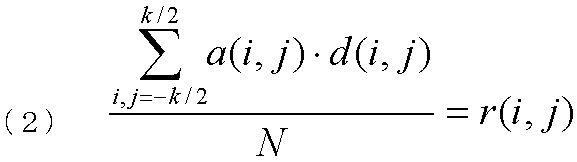
図13に示すように、注目画素を代表フレーム32内で移動させながら、その都度、関係式(2)を演算する。そして、代表フレーム32内のすべての画素についてそれぞれ得られた、未知の係数行列a(i,j)を用いて定義された関係式(2)を最も満足させる係数行列a(i,j)を求める。係数行列a(i,j)の要素数k×kは、適宜設定すればよい。少ないと精度が劣化し、多すぎると演算時間が長くなる。また、注目画素が代表フレーム32内を移動する際、端部に近いと端部側の周囲の画素が必要分存在しない場合もあるが、かかる場合には値が得られる周囲画素及び画素数Nで演算すればよい。
以上により、リサイズ量と丸め量の絞り込まれた複数の組み合わせの組み合わせ毎のフィルタ関数の係数行列a(i,j)が得られる。これらの複数の係数行列a(i,j)は、参照画像を作成するためのフィルタ関数の候補である。これらの複数の係数行列a(i,j)の中から真のフィルタ関数を選択する必要がある。
なお、一致度が閾値Tth未満の場合に、パラメータ範囲設定部62は、参照画像生成パラメータの予め設定されたデフォルトの範囲を設定する場合がある。かかる場合、フィルタ関数生成部64は、参照画像生成パラメータのデフォルトの範囲内の複数の参照画像生成パラメータのうちそれぞれ1つを用いて参照画像を作成するための複数のフィルタ関数の候補を生成する。このように一致度が低い場合には、参照画像生成パラメータの使用範囲は絞りこまれないようにできる。
階調差算出工程(S138)として、まず、参照回路112は、変更設定された、又は、絞り込まれた参照画像生成パラメータの範囲内で生成された複数のフィルタ関数の候補を用いて複数の参照画像の候補を作成する。具体的には、以下のように動作する。参照回路112は、リサイズ量と丸め量の絞り込まれた複数の組み合わせの組み合わせ毎に、当該組み合わせ用のフィルタ関数の候補を用いて、代表フレーム画像に対応する参照画像の候補を作成する。参照回路112は、まず、代表フレーム領域32の設計画像内のパターンに対して、当該組み合わせのリサイズと丸め処理を実施した上で、設計画像の画素毎に、当該画素d(i,i)を中心にして、k×k画素の画素と当該組み合わせ用のフィルタ関数となる係数行列a(i,j)との積の和を画素数N(=k×k)で割った参照画像データを作成する。得られた参照画像データは、フィルタ関数演算回路140に送られ、記憶装置75に格納される。
次に、階調差算出部80は、リサイズ量と丸め量の絞り込まれた複数の組み合わせの組み合わせ毎に、参照画像の画素値から測定画像の画素値を差し引いた階調差Δを算出する。かかる階調差は画像内の画素毎に算出される。
判定工程(S140)として、判定部82は、複数の参照画像の候補の参照画像毎の当該参照画像と代表フレーム画像(光学画像)との最大階調差Δmaxを用いて、最大階調差Δmaxが閾値ΔTh以下となる参照画像の候補の有無を判定する。最大階調差Δmaxは、当該画像内のすべての画素で得られた複数の階調差Δのうちの最大値を示す。
複数の参照画像の候補の中に最大階調差Δmaxが閾値ΔTh以下となる参照画像の候補が無い場合には、デフォルト設定工程(S142)に進む。最大階調差Δmaxが閾値ΔTh以下となる参照画像の候補が有る場合には、評価値算出工程(S144)に進む。
デフォルト設定工程(S142)として、パラメータ範囲設定部62は、複数の参照画像の候補のすべてにおいて、最大階調差Δmaxが閾値ΔThを超える場合に、参照画像生成パラメータのデフォルトの範囲を再設定する。言い換えれば、リサイズ量と丸め量の絞り込まれた複数の組み合わせでは、範囲が狭すぎたため、デフォルトの範囲に戻す設定を行う。そして、フィルタ関数生成工程(S131)に戻り、フィルタ関数生成部64は、再度、参照画像生成パラメータのデフォルトの範囲内の複数の参照画像生成パラメータのうちそれぞれ1つを用いて参照画像を作成するための複数のフィルタ関数の候補を生成する。そして、階調差算出工程(S138)と判定工程(S140)とを実施する。
評価値算出工程(S144)として、評価値算出部86は、最大階調差Δmaxが閾値ΔTh以下となる参照画像の候補を作成したフィルタ関数の評価値を算出する。評価値として、既に計算済の階調差Δを用いて、例えば、画像内の階調差の2乗和(差分2乗和)、或いは差分2乗和の平方根を用いると好適である。評価値として、最大階調差を用いる場合には、既に計算済なので、当該工程は省略する。算出された評価値は、上述したスコアの値として、参照画像生成パラメータと、フィルタ関数と共に、記録される。将来の試料の検査の際に過去データの1つとして使用されることになる。
フィルタ関数決定工程(S146)として、決定部84は、生成された複数のフィルタ関数の候補のうち参照画像を作成するための真のフィルタ関数を決定する。例えば、最大階調差Δmaxが閾値ΔTh以下となる参照画像の候補が1つであれば、当該参照画像作成に使用したフィルタ関数を真のフィルタ関数として決定する。例えば、最大階調差Δmaxが閾値ΔTh以下となる参照画像の候補が2以上存在する場合には、評価値算出工程(S144)で得られた評価値(例えば差分2乗和の平方根)が小さい方(スコア順位が高くなる方)の参照画像作成に使用したフィルタ関数を真のフィルタ関数として決定すると好適である。
以上のように、一致度に応じて参照画像生成パラメータの範囲を変更設定する、又は、絞り込むことによって、フィルタ関数生成に生じる処理量を低減し、時間を短縮できる。決定されたフィルタ関数(係数行列)は、参照回路に設定される。同様に、その際のリサイズ量及び丸め量が参照回路に設定される。そして、試料101全体の検査処理を開始する。
図14は、実施の形態1における比較回路の内部構成の一例を示す図である。図14において、比較回路108内には、磁気ディスク装置等の記憶装置50,52,56、フレーム画像作成部54、位置合わせ部57、及び比較部58が配置されている。フレーム画像作成部54、位置合わせ部57、及び比較部58といった一連の「~部」は、処理回路を有する。かかる処理回路には、電気回路、コンピュータ、プロセッサ、回路基板、量子回路、或いは、半導体装置等が含まれる。また、各「~部」は、共通する処理回路(同じ処理回路)を用いてもよい。或いは、異なる処理回路(別々の処理回路)を用いても良い。フレーム画像作成部54、位置合わせ部57、及び比較部58に必要な入力データ或いは演算された結果はその都度比較回路108内の図示しないメモリ若しくはメモリ115に記憶される。
ストライプ画像取得工程(S202)(スキャン工程、或いは光学画像取得工程ともいう。)として、光学画像取得機構150は、試料101となるフォトマスクの光学画像を取得する。ストライプ画像の取得方法は、上述した内容と同様である。但し、ここでは、図2に示すように順にストライプ画像を取得していく。そして、検査ストライプ20毎にストライプパターンメモリ123に画素データが格納される。その後、ストライプ領域画像は、位置回路107から出力されたXYθテーブル102上におけるフォトマスク101の位置を示すデータと共に比較回路108に送られる。測定データ(画素データ)は例えば8ビットの符号なしデータであり、各画素の明るさの階調(光量)を表現している。比較回路108内に出力されたストライプ領域画像は、記憶装置50に格納される。
フレーム画像作成工程(S204)として、比較回路108内では、フレーム画像作成部54が、所定の幅でストライプ領域画像(光学画像)が分割された複数のフレーム画像31を生成する。具体的には、図2に示すように、ストライプ領域画像は、矩形の複数のフレーム領域30のフレーム画像に分割される。例えば、512×512画素のサイズに分割される。各フレーム領域30のデータは、記憶装置56に格納される。
設計画像作成工程(S212)として、展開回路111(設計画像作成部)は、被検査試料101のパターン形成の基となる設計パターンデータに基づいて画像展開して設計画像を作成する。具体的には、展開回路111は、磁気ディスク装置109から制御計算機110を通して設計データを読み出し、読み出された設計データに定義された各フレーム領域30の各図形パターンを2値ないしは多値のイメージデータに変換する。そして、画素毎に8ビットの占有率データの設計画像を作成する。設計画像のデータ(イメージデータ)は参照回路112に出力される。
参照画像作成工程(S214)として、参照回路112(参照画像作成部)は、決定された真のフィルタ関数を用いて、光学画像と比較するための参照画像を作成する。具体的には、参照回路112は、設定されたリサイズ量及び丸め量によって設計画像をリサイズ及び丸め処理した上で、設定された係数行列a(i,j)(フィルタ関数の一例)を用いてフィルタ処理して参照画像を作成する。作成された参照画像は比較回路108に出力され、比較回路108内に出力された参照画像は、記憶装置52に格納される。以上により、検査のために比較される他方の画像(参照画像)データが生成される。
なお、代表フレームの代表設計画像を用いて演算された係数行列a(i,j)(フィルタ関数の一例)は、検査領域10内のフレーム領域30が互いに異なるすべての設計画像(複数の設計画像)のフィルタ処理に用いられる。言い換えれば、複数の設計画像は、演算された同じフィルタ関数を用いてそれぞれフィルタ処理される。
比較工程(S230)と、比較回路108(比較部の一例)は、撮像された光学画素と参照画像とを比較し、結果を出力する。具体的には、以下のように動作する。まず、位置合わせ部57は、比較対象となるフレーム画像(光学画像)を記憶装置56から読み出し、同様に比較対象となる参照画像を記憶装置52から読み出す。そして、所定のアルゴリズムで位置合わせを行う。例えば、最小2乗法を用いて位置合わせを行う。そして、比較部58は、所定の判定条件に従って画素毎に両者を比較し、例えば形状欠陥といった欠陥の有無を判定する。判定条件としては、例えば、所定のアルゴリズムに従って画素毎に両者を比較し、欠陥の有無を判定する。そして、比較結果が出力される。比較結果は、例えば、磁気ディスク装置109、フレキシブルディスク装置(FD)115、CRT117、パターンモニタ118に出力される、或いはプリンタ119から出力されればよい。
図15は、実施の形態1の変形例における参照画像生成パラメータ範囲と設定された結果との一例を示す図である。図15の例では、縦軸に丸め量を示し、横軸にリサイズ量を示す。図8の例では、スコアの小さい方から順に、一致度に応じたN%に変更設定された、又は、絞り込んだ複数の組み合わせをそのまま使用する場合を示したが、これに限るものではない。図15に示すように、N%に変更設定された、又は、絞り込んだ複数の組み合わせの外接矩形を設定し、かかる外接矩形内の組み合わせを変更設定された、又は、絞り込まれたパラメータの組み合わせとして設定しても好適である。図15の例では、リサイズ量の範囲として、Ai~Asとし、Ai~As内の所定の間隔のすべてのリサイズ量を使用する。また、丸め量の範囲として、Bj~Btとし、Bj~Bt内の所定の間隔のすべての丸め量を使用する。
以上のように、実施の形態1によれば、今回の検査に適したフィルタ関数を得るまでの処理量を低減できる。引いては今回の検査に適したフィルタ関数を得るまでの処理時間を短縮できる。
以上、具体例を参照しつつ実施の形態について説明した。しかし、本発明は、これらの具体例に限定されるものではない。例えば、実施の形態では、照明光学系170として、透過光を用いた透過照明光学系を示したが、これに限るものではない。例えば、反射光を用いた反射照明光学系であってもよい。或いは、透過照明光学系と反射照明光学系とを組み合わせて、透過光と反射光を同時に用いてもよい。
また、上述したフィルタ関数及びフィルタ関数の係数は一例であって、これに限るものではない。その他のフィルタ関数及びフィルタ関数の係数を用いる場合であっても良い。
また、装置構成や制御手法等、本発明の説明に直接必要しない部分等については記載を省略したが、必要とされる装置構成や制御手法を適宜選択して用いることができる。例えば、検査装置100を制御する制御部構成については、記載を省略したが、必要とされる制御部構成を適宜選択して用いることは言うまでもない。
その他、本発明の要素を具備し、当業者が適宜設計変更しうる全てのパターン検査装置、及びパターン検査方法は、本発明の範囲に包含される。
本発明の一態様は、パターン検査装置及びパターン検査方法に関する。例えば、半導体製造に用いる試料となる物体のパターン欠陥を検査するパターン検査技術に関し、半導体素子を製作するときに使用されるマスクの欠陥を検査する方法に利用できる。
10 検査領域
20 検査ストライプ
30 フレーム領域
31 フレーム画像
32 代表フレーム
54 フレーム画像作成部
57 位置合わせ部
58 比較部
60 一致度算出部
61,70,71,73,75 記憶装置
62 パラメータ範囲設定部
64 フィルタ関数生成部
66 リサイズ処理部
67 丸め処理部
68 フィルタ係数算出部
72 フレーム画像作成部
80 階調差算出部
82 判定部
84 決定部
86 評価値算出部
100 検査装置
101 試料
102 XYθテーブル
103 光源
104 拡大光学系
105 フォトダイオードアレイ
106 センサ回路
107 位置回路
108 比較回路
109 磁気ディスク装置
110 制御計算機
111 展開回路
112 参照回路
113 オートローダ制御回路
114 テーブル制御回路
115 FD
116 メモリ
117 CRT
118 パターンモニタ
119 プリンタ
120 バス
122 レーザ測長システム
123 ストライプパターンメモリ
130 オートローダ
140 係数演算回路
150 光学画像取得部
160 制御系回路
170 照明光学系
Claims (12)
- パターン形成された被検査試料の光学画像を取得する光学画像取得機構と、
過去の検査条件パラメータとの一致度に応じて、参照画像生成パラメータの範囲を設定するパラメータ範囲設定回路と、
設定された前記参照画像生成パラメータの範囲内の値を用いて、複数のフィルタ関数の候補を生成するフィルタ関数生成回路と、
生成された前記複数のフィルタ関数の候補のうち、参照画像を作成するためのフィルタ関数を決定する決定回路と、
決定された前記フィルタ関数を用いて、参照画像を作成する参照画像作成回路と、
前記光学画像と前記参照画像とを比較する比較回路と、
を備えたことを特徴とするパターン検査装置。 - 前記参照画像生成パラメータは、リサイズ量とコーナー丸め量の少なくとも1つであることを特徴とする請求項1記載のパターン検査装置。
- 前記参照画像生成パラメータの範囲は、予め設定されたデフォルトの範囲よりも絞り込まれた範囲に設定されることを特徴とする請求項1記載のパターン検査装置。
- 前記パラメータ範囲設定回路は、前記一致度が閾値未満の場合に、前記参照画像生成パラメータの予め設定されたデフォルトの範囲を設定し、
前記フィルタ関数生成回路は、前記参照画像生成パラメータのデフォルトの範囲内の複数の参照画像生成パラメータのうちそれぞれ1つを用いて参照画像を作成するための前記複数のフィルタ関数の候補を生成することを特徴とする請求項1記載のパターン検査装置。 - パターン条件のパラメータと撮像条件のパラメータとの少なくとも一方を用いて前記一致度を算出する一致度算出回路をさらに備えたことを特徴とする請求項1記載のパターン検査装置。
- 設定された前記参照画像生成パラメータの範囲内で生成された前記複数のフィルタ関数の候補を用いて、前記参照画像作成部により作成された複数の参照画像の候補毎の当該参照画像と光学画像との最大階調差を用いて、最大階調差が閾値以下となる参照画像の候補の有無を判定する判定回路をさらに備え、
前記パラメータ範囲設定回路は、前記複数の参照画像の候補のすべてにおいて、前記最大階調差が閾値を超える場合に、前記参照画像生成パラメータの予め設定されたデフォルトの範囲を再設定し、
前記フィルタ関数生成回路は、再度、前記参照画像生成パラメータのデフォルトの範囲内の複数の参照画像生成パラメータのうちそれぞれ1つを用いて参照画像を作成するための前記複数のフィルタ関数の候補を生成することを特徴とする請求項1記載のパターン検査装置。 - パターン形成された被検査試料の光学画像を取得し、
過去の検査条件パラメータとの一致度に応じて、参照画像生成パラメータの範囲を設定し、
設定された前記参照画像生成パラメータの範囲内の値を用いて、複数のフィルタ関数の候補を生成し、
生成された前記複数の前記フィルタ関数の候補のうち、参照画像を作成するためのフィルタ関数を決定し、
決定された前記フィルタ関数を用いて、参照画像を作成し、
前記光学画像と前記参照画像とを比較し、結果を出力する、
ことを特徴とするパターン検査方法。 - 前記参照画像生成パラメータは、リサイズ量とコーナー丸め量の少なくとも1つであることを特徴とする請求項7記載のパターン検査方法。
- 対象の前記参照画像生成パラメータの範囲は、予め設定されたデフォルトの範囲よりも絞り込まれた範囲に設定されることを特徴とする請求項7記載のパターン検査方法。
- 前記パラメータ範囲設定回路は、前記一致度が閾値未満の場合に、前記参照画像生成パラメータの予め設定されたデフォルトの範囲を設定し、
前記参照画像生成パラメータのデフォルトの範囲内の複数の参照画像生成パラメータのうちそれぞれ1つを用いて参照画像を作成するための前記複数のフィルタ関数の候補が生成されることを特徴とする請求項7記載のパターン検査方法。 - パターン条件のパラメータと撮像条件のパラメータとの少なくとも一方を用いて前記一致度を算出する、ことを特徴とする請求項7記載のパターン検査方法。
- 設定された前記参照画像生成パラメータの範囲内で生成された前記複数のフィルタ関数の候補を用いて、前記参照画像作成部により作成された複数の参照画像の候補毎の当該参照画像と光学画像との最大階調差を用いて、最大階調差が閾値以下となる参照画像の候補の有無を判定し、
前記複数の参照画像の候補のすべてにおいて、前記最大階調差が閾値を超える場合に、前記参照画像生成パラメータの予め設定されたデフォルトの範囲が再設定され、
再度、前記参照画像生成パラメータのデフォルトの範囲内の複数の参照画像生成パラメータのうちそれぞれ1つを用いて参照画像を作成するための前記複数のフィルタ関数の候補が生成されことを特徴とする請求項7記載のパターン検査方法。
Priority Applications (2)
| Application Number | Priority Date | Filing Date | Title |
|---|---|---|---|
| CN202480037823.3A CN121263679A (zh) | 2023-06-09 | 2024-05-14 | 图案检查装置以及图案检查方法 |
| US19/407,043 US20260086043A1 (en) | 2023-06-09 | 2025-12-03 | Pattern inspection apparatus and pattern inspection method |
Applications Claiming Priority (2)
| Application Number | Priority Date | Filing Date | Title |
|---|---|---|---|
| JP2023-095655 | 2023-06-09 | ||
| JP2023095655A JP2024176833A (ja) | 2023-06-09 | 2023-06-09 | パターン検査装置及びパターン検査方法 |
Related Child Applications (1)
| Application Number | Title | Priority Date | Filing Date |
|---|---|---|---|
| US19/407,043 Continuation US20260086043A1 (en) | 2023-06-09 | 2025-12-03 | Pattern inspection apparatus and pattern inspection method |
Publications (1)
| Publication Number | Publication Date |
|---|---|
| WO2024252865A1 true WO2024252865A1 (ja) | 2024-12-12 |
Family
ID=93795318
Family Applications (1)
| Application Number | Title | Priority Date | Filing Date |
|---|---|---|---|
| PCT/JP2024/017787 Ceased WO2024252865A1 (ja) | 2023-06-09 | 2024-05-14 | パターン検査装置及びパターン検査方法 |
Country Status (4)
| Country | Link |
|---|---|
| US (1) | US20260086043A1 (ja) |
| JP (1) | JP2024176833A (ja) |
| CN (1) | CN121263679A (ja) |
| WO (1) | WO2024252865A1 (ja) |
Citations (2)
| Publication number | Priority date | Publication date | Assignee | Title |
|---|---|---|---|---|
| JP2017058190A (ja) * | 2015-09-15 | 2017-03-23 | 株式会社ニューフレアテクノロジー | 参照画像作成用の基準データ作成方法及びパターン検査装置 |
| JP2019086590A (ja) * | 2017-11-02 | 2019-06-06 | 株式会社ニューフレアテクノロジー | パターン検査方法およびパターン検査装置 |
-
2023
- 2023-06-09 JP JP2023095655A patent/JP2024176833A/ja active Pending
-
2024
- 2024-05-14 CN CN202480037823.3A patent/CN121263679A/zh active Pending
- 2024-05-14 WO PCT/JP2024/017787 patent/WO2024252865A1/ja not_active Ceased
-
2025
- 2025-12-03 US US19/407,043 patent/US20260086043A1/en active Pending
Patent Citations (2)
| Publication number | Priority date | Publication date | Assignee | Title |
|---|---|---|---|---|
| JP2017058190A (ja) * | 2015-09-15 | 2017-03-23 | 株式会社ニューフレアテクノロジー | 参照画像作成用の基準データ作成方法及びパターン検査装置 |
| JP2019086590A (ja) * | 2017-11-02 | 2019-06-06 | 株式会社ニューフレアテクノロジー | パターン検査方法およびパターン検査装置 |
Also Published As
| Publication number | Publication date |
|---|---|
| CN121263679A (zh) | 2026-01-02 |
| US20260086043A1 (en) | 2026-03-26 |
| JP2024176833A (ja) | 2024-12-19 |
Similar Documents
| Publication | Publication Date | Title |
|---|---|---|
| US9177372B2 (en) | Defect estimation device and method and inspection system and method | |
| US10192304B2 (en) | Method for measuring pattern width deviation, and pattern inspection apparatus | |
| JP6637375B2 (ja) | パターン検査方法及びパターン検査装置 | |
| JP6132658B2 (ja) | 検査感度評価方法 | |
| JP4323475B2 (ja) | 試料検査装置、試料検査方法及びプログラム | |
| US9021406B2 (en) | Pattern inspection method of semiconductor device optical image | |
| JP7822184B2 (ja) | マスク検査装置及びマスク検査方法 | |
| JP7751504B2 (ja) | パターン検査方法、及びパターン検査装置 | |
| WO2024252865A1 (ja) | パターン検査装置及びパターン検査方法 | |
| JP7144262B2 (ja) | パターン検査装置及び参照画像の作成方法 | |
| JP6533062B2 (ja) | パターン検査方法 | |
| JP7222671B2 (ja) | パターン検査装置及びパターン検査方法 | |
| TWI686673B (zh) | 檢查方法 | |
| WO2025192130A1 (ja) | パターン検査装置及びパターン検査方法 | |
| JP2025186098A (ja) | パターン検査装置、及びパターン検査方法 | |
| JP7465138B2 (ja) | パターン検査装置及びパターン検査方法 | |
| JP4185515B2 (ja) | 試料検査方法、プログラム及び試料検査装置 | |
| JP2025065903A (ja) | パターン検査装置、焦点位置調整方法、及びパターン検査方法 | |
| JP6851178B2 (ja) | パターン検査方法及びパターン検査装置 |
Legal Events
| Date | Code | Title | Description |
|---|---|---|---|
| 121 | Ep: the epo has been informed by wipo that ep was designated in this application |
Ref document number: 24819102 Country of ref document: EP Kind code of ref document: A1 |
|
| NENP | Non-entry into the national phase |
Ref country code: DE |