WO2024252869A1 - 半導体装置および車両 - Google Patents
半導体装置および車両 Download PDFInfo
- Publication number
- WO2024252869A1 WO2024252869A1 PCT/JP2024/017938 JP2024017938W WO2024252869A1 WO 2024252869 A1 WO2024252869 A1 WO 2024252869A1 JP 2024017938 W JP2024017938 W JP 2024017938W WO 2024252869 A1 WO2024252869 A1 WO 2024252869A1
- Authority
- WO
- WIPO (PCT)
- Prior art keywords
- terminal
- semiconductor device
- electrode
- semiconductor
- conductive member
- Prior art date
- Legal status (The legal status is an assumption and is not a legal conclusion. Google has not performed a legal analysis and makes no representation as to the accuracy of the status listed.)
- Ceased
Links
Images











Classifications
-
- H—ELECTRICITY
- H10—SEMICONDUCTOR DEVICES; ELECTRIC SOLID-STATE DEVICES NOT OTHERWISE PROVIDED FOR
- H10W—GENERIC PACKAGES, INTERCONNECTIONS, CONNECTORS OR OTHER CONSTRUCTIONAL DETAILS OF DEVICES COVERED BY CLASS H10
- H10W40/00—Arrangements for thermal protection or thermal control
- H10W40/40—Arrangements for thermal protection or thermal control involving heat exchange by flowing fluids
- H10W40/47—Arrangements for thermal protection or thermal control involving heat exchange by flowing fluids by flowing liquids, e.g. forced water cooling
-
- H—ELECTRICITY
- H02—GENERATION; CONVERSION OR DISTRIBUTION OF ELECTRIC POWER
- H02M—APPARATUS FOR CONVERSION BETWEEN AC AND AC, BETWEEN AC AND DC, OR BETWEEN DC AND DC, AND FOR USE WITH MAINS OR SIMILAR POWER SUPPLY SYSTEMS; CONVERSION OF DC OR AC INPUT POWER INTO SURGE OUTPUT POWER; CONTROL OR REGULATION THEREOF
- H02M7/00—Conversion of AC power input into DC power output; Conversion of DC power input into AC power output
- H02M7/42—Conversion of DC power input into AC power output without possibility of reversal
- H02M7/44—Conversion of DC power input into AC power output without possibility of reversal by static converters
- H02M7/48—Conversion of DC power input into AC power output without possibility of reversal by static converters using discharge tubes with control electrode or semiconductor devices with control electrode
-
- H—ELECTRICITY
- H10—SEMICONDUCTOR DEVICES; ELECTRIC SOLID-STATE DEVICES NOT OTHERWISE PROVIDED FOR
- H10W—GENERIC PACKAGES, INTERCONNECTIONS, CONNECTORS OR OTHER CONSTRUCTIONAL DETAILS OF DEVICES COVERED BY CLASS H10
- H10W70/00—Package substrates; Interposers; Redistribution layers [RDL]
- H10W70/40—Leadframes
- H10W70/421—Shapes or dispositions
- H10W70/424—Cross-sectional shapes
- H10W70/427—Bent parts
- H10W70/429—Bent parts being the outer leads
-
- H—ELECTRICITY
- H10—SEMICONDUCTOR DEVICES; ELECTRIC SOLID-STATE DEVICES NOT OTHERWISE PROVIDED FOR
- H10W—GENERIC PACKAGES, INTERCONNECTIONS, CONNECTORS OR OTHER CONSTRUCTIONAL DETAILS OF DEVICES COVERED BY CLASS H10
- H10W90/00—Package configurations
Definitions
- This disclosure relates to a semiconductor device and a vehicle equipped with the semiconductor device.
- Patent Document 1 discloses an example of a semiconductor module that includes a semiconductor device and a cooler.
- the cooler includes a housing having a hollow region and a heat sink.
- the housing has an opening that leads to the hollow region.
- the heat sink is attached to the housing so as to cover the opening.
- a part of the heat sink is contained in the hollow region.
- the semiconductor device is joined to a part of the heat sink that protrudes from the hollow region. When a coolant (such as cooling water) is flowed through the hollow region, the coolant comes into contact with the heat sink. This allows the semiconductor device to be efficiently cooled via the heat sink.
- a coolant such as cooling water
- An object of the present disclosure is to provide a semiconductor device that is an improvement over conventional semiconductor devices.
- an object of the present disclosure is to provide a semiconductor device that can further improve cooling efficiency.
- the semiconductor device provided by the first aspect of the present disclosure comprises a semiconductor element and a first terminal located on one side of the semiconductor element in a first direction and conductive to the semiconductor element.
- a first flow passage is provided between the semiconductor element and the first terminal in the first direction. The semiconductor element is in contact with the first flow passage.
- the vehicle provided by the second aspect of the present disclosure includes a drive source and a semiconductor device.
- the semiconductor device is electrically connected to the drive source.
- the semiconductor device further includes a second terminal and a signal terminal compared to the semiconductor device provided by the first aspect of the present disclosure.
- the semiconductor element included in the semiconductor device includes a first electrode, a second electrode, and a gate electrode.
- the first conductive member included in the semiconductor device is electrically connected to the first electrode.
- the second terminal is electrically connected to the second electrode.
- the signal terminal is electrically connected to the gate electrode.
- the above configuration makes it possible to further improve the cooling efficiency of semiconductor devices.
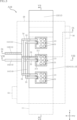
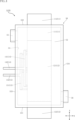
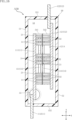
- FIG. 1 is a plan view of a semiconductor device according to a first embodiment of the present disclosure.
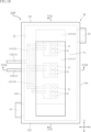
- FIG. 2 is a plan view corresponding to FIG. 1, seen through the housing.
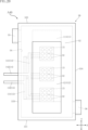
- FIG. 3 is a plan view corresponding to FIG. 2, further showing the first terminal in a transparent manner.
- FIG. 4 is a bottom view of the semiconductor device shown in FIG.
- FIG. 5 is a right side view of the semiconductor device shown in FIG.
- FIG. 6 is a left side view of the semiconductor device shown in FIG.
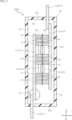
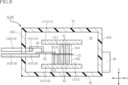
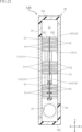
- FIG. 7 is a cross-sectional view taken along line VII-VII in FIG.
- FIG. 8 is a cross-sectional view taken along line VIII-VIII in FIG.
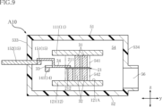
- FIG. 9 is a cross-sectional view taken along line IX-IX in FIG.
- FIG. 1 is a plan view of a semiconductor device according to a first embodiment of the present disclosure.
- FIG. 2 is a plan view corresponding to FIG. 1, seen through the housing.
- FIG. 3 is a plan
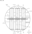
- FIG. 10 is a partially enlarged view of FIG.
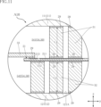
- FIG. 11 is a partially enlarged view of FIG.
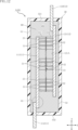
- FIG. 12 is a cross-sectional view illustrating the function and effect of the semiconductor device shown in FIG.
- FIG. 13 is a cross-sectional view of a semiconductor device according to a second embodiment of the present disclosure, and corresponds to FIG.
- FIG. 14 is a cross-sectional view of the semiconductor device shown in FIG. 13 and corresponds to FIG.
- FIG. 15 is a partially enlarged view of FIG.
- FIG. 16 is a cross-sectional view of a semiconductor device according to a third embodiment of the present disclosure, and corresponds to FIG.
- FIG. 17 is a cross-sectional view of the semiconductor device shown in FIG. 16 and corresponds to FIG. FIG.
- FIG. 18 is a partially enlarged view of FIG.
- FIG. 19 is a plan view of a semiconductor device according to a fourth embodiment of the present disclosure.
- 20 is a bottom view of the semiconductor device shown in FIG.
- FIG. 21 is a cross-sectional view taken along line XXI-XXI in FIG.
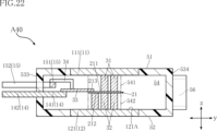
- FIG. 22 is a cross-sectional view taken along line XXII-XXII in FIG.
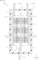
- FIG. 23 is a plan view of a semiconductor device according to a fifth embodiment of the present disclosure, seen through the housing.
- FIG. 24 is a cross-sectional view taken along line XXIV-XXIV in FIG.
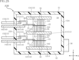
- FIG. 25 is a cross-sectional view taken along line XXV-XXV in FIG.
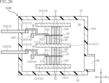
- FIG. 26 is a cross-sectional view taken along line XXVI-XXVI in FIG.
- FIG. 27 is a partially enlarged view of FIG.
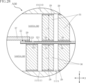
- FIG. 28 is a partially enlarged view of FIG.
- FIG. 29 is a schematic diagram of a vehicle on which the semiconductor device shown in FIG. 23 is mounted.
- a semiconductor device A10 according to a first embodiment of the present disclosure will be described with reference to FIGS. 1 to 11.
- the semiconductor device A10 is generally used in a power conversion circuit such as an inverter.
- the semiconductor device A10 includes a first terminal 11, a second terminal 12, a first signal terminal 14, a second signal terminal 15, a plurality of first semiconductor elements 21, a plurality of first conductive members 31, a plurality of second conductive members 32, a plurality of third conductive members 33, a plurality of fourth conductive members 34, and a housing 50.
- FIG. 2 shows the housing 50 through the view for ease of understanding.
- the transparent housing 50 is shown by an imaginary line (two-dot chain line).
- the first terminal 11 and the housing 50 are shown through the view for ease of understanding.
- each of the transparent first terminal 11 and the housing 50 is shown by an imaginary line.
- first direction z the normal direction of the first mounting surface 121A of the second terminal 12 described later is referred to as the "first direction z.”
- second direction x One direction perpendicular to the first direction z
- third direction y A direction perpendicular to both the first direction z and the second direction x is referred to as the "third direction y.”
- the housing 50 supports each of the first terminal 11, the second terminal 12, the first signal terminal 14, and the second signal terminal 15.
- the housing 50 is made of an insulator that contains resin.
- the housing 50 may be made of a conductor that contains a metal such as aluminum (Al).
- the housing 50 has a top surface 51, a bottom surface 52, a first side surface 531, a second side surface 532, a third side surface 533 and a fourth side surface 534.
- the top surface 51 faces one side in the first direction z.
- the bottom surface 52 faces the opposite side to the top surface 51 in the first direction z.
- the first side surface 531 and the second side surface 532 face opposite each other in the second direction x.
- the third side surface 533 and the fourth side surface 534 face opposite each other in the third direction y.
- the housing 50 has a hollow portion 54. Atmosphere flows into the hollow portion 54.
- the hollow portion 54 may be constantly filled with the coolant 60.
- the hollow portion 54 includes a first flow passage 541 and a second flow passage 542.
- the first flow passage 541 is provided between the first semiconductor elements 21 and the first terminal 11 in the first direction z.
- the second flow passage 542 is provided between the first semiconductor elements 21 and the second terminal 12 in the first direction z.
- the coolant 60 shown in FIG. 12 must be an insulator.
- the composition of the coolant 60 is not limited as long as the coolant 60 is an insulator.
- the housing 50 is provided with an inlet 55 and an outlet 56.
- the inlet 55 opens at the third side surface 533 and communicates with the hollow portion 54.
- the outlet 56 opens at the fourth side surface 534 and communicates with the hollow portion 54.
- the refrigerant 60 shown in Figure 12 flows into the hollow portion 54 from the inlet 55.
- the refrigerant 60 that has flowed into the hollow portion 54 is discharged from the outlet 56.
- the inlet 55 and the outlet 56 are located on opposite sides of each other in the third direction y with respect to the multiple first conductive members 31.
- the first terminal 11 is located on one side of the multiple first semiconductor elements 21 in the first direction z.
- the first terminal 11 is located between the multiple first semiconductor elements 21 and the top surface 51 of the housing 50 in the first direction z.
- the first terminal 11 is a metal plate containing, for example, copper (Cu).
- the first terminal 11 has a first base 111 and a first extension 112.
- the first base 111 is housed in the hollow portion 54 of the housing 50 and is in contact with the first flow passage 541.
- the first base 111 is strip-shaped extending in the second direction x.
- the first extension 112 is conductively joined to one side of the first base 111 in the second direction x.
- the first extension 112 is supported by the housing 50. A part of the first extension 112 protrudes to the outside from the second side surface 532 of the housing 50.
- the second terminal 12 is located on the opposite side of the first terminal 11 in the first direction z with respect to the multiple first semiconductor elements 21.
- the second terminal 12 is located between the multiple first semiconductor elements 21 and the bottom surface 52 of the housing 50 in the first direction z.
- the second terminal 12 is a metal plate containing, for example, copper.
- the second terminal 12 has a second base 121 and a second extension 122.
- the second base 121 is housed in the hollow portion 54 of the housing 50 and is in contact with the second flow passage 542.
- the second base 121 is strip-shaped extending in the second direction x.
- the second base 121 has a first mounting surface 121A that faces the same side as the top surface 51 of the housing 50 in the first direction z.
- the second extension 122 is conductively joined to one side of the second base 121 in the second direction x.
- the second extension section 122 is supported by the housing 50. A portion of the second extension section 122 protrudes outward from the first side surface 531 of the housing 50.
- the multiple first semiconductor elements 21 are positioned between the first base 111 of the first terminal 11 and the second base 121 of the second terminal 12 in the first direction z.
- the multiple first semiconductor elements 21 are housed in the hollow portion 54 of the housing 50.
- Each of the multiple first semiconductor elements 21 is in contact with each of the first flow passage 541 and the second flow passage 542.
- each of the multiple first semiconductor elements 21 overlaps the first mounting surface 121A of the second base 121. All of the multiple first semiconductor elements 21 are the same element.
- the multiple first semiconductor elements 21 are, for example, MOSFETs (Metal-Oxide-Semiconductor Field-Effect Transistors).
- the multiple first semiconductor elements 21 may be field effect transistors including metal-insulator-semiconductor field-effect transistors (MISFETs) or bipolar transistors such as insulated gate bipolar transistors (IGBTs).
- MISFETs metal-insulator-semiconductor field-effect transistors
- IGBTs insulated gate bipolar transistors
- the multiple first semiconductor elements 21 are n-channel type MOSFETs with a vertical structure.
- the multiple first semiconductor elements 21 include a compound semiconductor substrate.
- the composition of the compound semiconductor substrate includes silicon carbide (SiC).
- the multiple first semiconductor elements 21 are arranged along the second direction x.
- each of the multiple first semiconductor elements 21 has a first electrode 211, a second electrode 212, and a first gate electrode 213.
- the first electrode 211 is located on the side facing the first base 111 of the first terminal 11 in the first direction z.
- the first electrode 211 is electrically connected to the first terminal 11.
- a current corresponding to the power converted by the first semiconductor element 21 flows through the first electrode 211.
- the first electrode 211 corresponds to the source of the first semiconductor element 21.
- the first electrode 211 is in contact with the first flow path 541.
- the second electrode 212 faces the second base 121 of the second terminal 12 in the first direction z.
- the second electrode 212 is electrically connected to the second terminal 12.
- a current corresponding to the power before being converted by the first semiconductor element 21 flows through the second electrode 212.
- the second electrode 212 corresponds to the drain of the first semiconductor element 21.
- the second electrode 212 is in contact with the second flow path 542.
- the first gate electrode 213 is located on the same side as the first electrode 211 in the first direction z.
- the first gate electrode 213 is conductive to the first signal terminal 14.
- a gate voltage for driving the first semiconductor element 21 is applied to the first gate electrode 213.
- the area of the first gate electrode 213 is smaller than the area of the first electrode 211 when viewed in the first direction z.
- Each of the multiple first conductive members 31 is electrically connected to one of the first electrodes 211 of each of the multiple first semiconductor elements 21 and the first terminal 11. As shown in Figures 7 to 9, the multiple first conductive members 31 are located between the multiple first semiconductor elements 21 and the first base portion 111 of the first terminal 11 in the first direction z. The multiple first conductive members 31 are housed in the first flow passage 541. The multiple first conductive members 31 are metal pieces containing copper, for example. Each of the multiple first conductive members 31 is, for example, cylindrical. As shown in Figures 10 and 11, one side of each of the multiple first conductive members 31 in the first direction z is electrically connected to the first electrode 211 of one of the multiple first semiconductor elements 21 via a bonding layer 29. The bonding layer 29 is solder.
- the bonding layer 29 may be a sintered metal containing silver (Ag) or the like.
- the other side of each of the multiple first conductive members 31 in the first direction z is electrically connected to the first base portion 111 of the first terminal 11 via the bonding layer 29.
- the dimension L1 of each of the multiple first conductive members 31 in the first direction z is greater than the dimension of each of the multiple first conductive members 31 in a direction perpendicular to the first direction z.
- Each of the multiple second conductive members 32 is electrically connected to one of the second electrodes 212 of each of the multiple first semiconductor elements 21 and the second terminal 12. As shown in Figures 7 to 9, the multiple second conductive members 32 are located between the multiple first semiconductor elements 21 and the second base 121 of the second terminal 12 in the first direction z. The multiple second conductive members 32 are accommodated in the second flow passage 542. The multiple second conductive members 32 are metal pieces containing copper, for example. Each of the multiple second conductive members 32 is, for example, cylindrical. As shown in Figures 10 and 11, one side of each of the multiple second conductive members 32 in the first direction z is electrically connected to the second electrode 212 of one of the multiple first semiconductor elements 21 via the bonding layer 29.
- each of the multiple second conductive members 32 in the first direction z is electrically connected to the first mounting surface 121A of the second base 121 via the bonding layer 29.
- the dimension L2 in the first direction z of each of the multiple second conductive members 32 is greater than the dimension in the direction perpendicular to the first direction z of each of the multiple second conductive members 32.
- the first signal terminal 14 is located on one side of the first terminal 11 in the third direction y.
- the first signal terminal 14 is supported by the housing 50.
- the first signal terminal 14 is electrically connected to the first gate electrode 213 of each of the first semiconductor elements 21.
- a gate voltage for driving the first semiconductor elements 21 is applied to the first signal terminal 14.
- the first signal terminal 14 is, for example, a metal lead containing copper.
- the first signal terminal 14 has an inner part 141 and an outer part 142.
- the inner part 141 is accommodated in the housing 50.
- a part of the inner part 141 is accommodated in the hollow part 54 of the housing 50.
- the inner part 141 includes a part extending in the second direction x.
- the outer part 142 is connected to the inner part 141.
- the outer part 142 protrudes to the outside from the third side surface 533 of the housing 50.
- Each of the multiple third conductive members 33 is electrically connected to one of the first gate electrodes 213 of each of the multiple first semiconductor elements 21 and the first signal terminal 14. As shown in FIG. 3, each of the multiple third conductive members 33 extends in the third direction y. A portion of each of the multiple third conductive members 33 is accommodated in the first flow passage 541.
- the multiple third conductive members 33 are metal leads containing copper, for example.
- One side of each of the multiple third conductive members 33 in the third direction y is electrically connected to one of the first gate electrodes 213 of the multiple first semiconductor elements 21 via the bonding layer 29.
- the other side of each of the multiple third conductive members 33 in the first direction z is electrically connected to the inner portion 141 of the first signal terminal 14.
- the second signal terminal 15 is located on the same side as the first signal terminal 14 with respect to the first terminal 11 in the third direction y.
- the second signal terminal 15 is supported by the housing 50.
- the second signal terminal 15 is electrically connected to the first electrodes 211 of each of the multiple first semiconductor elements 21.
- a voltage having the same potential as the voltage applied to the first electrodes 211 of each of the multiple first semiconductor elements 21 is applied to the second signal terminal 15.
- the second signal terminal 15 is, for example, a metal lead containing copper.
- the second signal terminal 15 has an inner portion 151 and an outer portion 152.
- the inner portion 151 is accommodated in the housing 50.
- a portion of the inner portion 151 is accommodated in the hollow portion 54 of the housing 50.
- the inner portion 151 includes a portion extending in the second direction x. As shown in Figures 8 and 9, the inner part 151 is located closer to the top surface 51 of the housing 50 than the inner part 141 of the first signal terminal 14.
- the outer part 152 is connected to the inner part 151. As shown in Figures 6 and 9, the outer part 152 protrudes outward from the third side surface 533 of the housing 50.
- Each of the multiple fourth conductive members 34 is electrically connected to one of the first electrodes 211 of each of the multiple first semiconductor elements 21 and the second signal terminal 15. As shown in FIG. 3, when viewed in the first direction z, each of the multiple fourth conductive members 34 extends in the third direction y. As shown in FIG. 9, each of the multiple fourth conductive members 34 straddles the inner part 141 of the first signal terminal 14. A part of each of the multiple fourth conductive members 34 is accommodated in the first flow passage 541.
- the multiple fourth conductive members 34 are metal leads containing copper, for example.
- One side of each of the multiple fourth conductive members 34 in the third direction y is electrically connected to one of the first electrodes 211 of the multiple first semiconductor elements 21.
- the other side of each of the multiple fourth conductive members 34 in the first direction z is electrically connected to the inner part 151 of the second signal terminal 15.
- the semiconductor device A10 includes a first semiconductor element 21 and a first terminal 11.
- the first terminal 11 is located on one side of the first semiconductor element 21 in the first direction z and is conductive to the first terminal 11.
- a first flow passage 541 is provided between the first semiconductor element 21 and the first terminal 11 in the first direction z.
- the first semiconductor element 21 is in contact with the first flow passage 541.
- the semiconductor device A10 further includes a first conductive member 31 that is electrically connected to the first semiconductor element 21 and the first terminal 11.
- the first conductive member 31 is housed in the first flow passage 541. With this configuration, the coolant 60 comes into direct contact with the first conductive member 31. This allows the heat conducted from the first semiconductor element 21 to the first conductive member 31 to be efficiently released to the outside.
- the first electrode 211 of the first semiconductor element 21 is in contact with the first flow passage 541. With this configuration, the coolant 60 comes into direct contact with the first electrode 211. This allows the heat generated by the first semiconductor element 21 to be efficiently released to the outside.
- the dimension L1 of the first conductive member 31 in the first direction z is greater than the dimension of the first conductive member 31 in a direction perpendicular to the first direction z. This configuration reduces the energy loss of the flow of the refrigerant 60 caused by the sudden contraction of the first flow passage 541 due to the first conductive member 31.
- the semiconductor device A10 further includes a second terminal 12 and a second conductive member 32.
- a second flow passage 542 is provided between the first semiconductor element 21 and the second terminal 12 in the first direction z.
- the second conductive member 32 is housed in the second flow passage 542.
- the first semiconductor element 21 is in contact with the second flow passage 542.
- the second electrode 212 of the first semiconductor element 21 is in contact with the second flow passage 542. With this configuration, the coolant 60 comes into direct contact with the second electrode 212. This allows the heat generated by the first semiconductor element 21 to be released to the outside more efficiently.
- the dimension L2 of the second conductive member 32 in the first direction z is greater than the dimension of the second conductive member 32 in a direction perpendicular to the first direction z. This configuration reduces the energy loss of the flow of the refrigerant 60 caused by the sudden contraction of the second flow passage 542 due to the second conductive member 32.
- the semiconductor device A10 further includes a housing 50 that supports each of the first terminal 11 and the second terminal 12.
- the housing 50 is provided with an inlet 55 and an outlet 56.
- the inlet 55 and the outlet 56 are located on opposite sides of each other with respect to the first conductive member 31 in a direction perpendicular to the first direction z.
- FIG. 13 corresponds to the cross-sectional position in Figure 7 showing the semiconductor device A10.
- FIG. 14 corresponds to the cross-sectional position in Figure 8 showing the semiconductor device A10.
- the semiconductor device A20 differs from the semiconductor device A10 in that it does not have multiple second conductive members 32.
- the second electrode 212 of each of the multiple first semiconductor elements 21 is conductively bonded to the first mounting surface 121A of the second base 121 of the second terminal 12 via a bonding layer 29.
- the semiconductor device A20 includes a first semiconductor element 21 and a first terminal 11.
- the first terminal 11 is located on one side of the first semiconductor element 21 in the first direction z and is conductive to the first terminal 11.
- a first flow passage 541 is provided between the first semiconductor element 21 and the first terminal 11 in the first direction z.
- the first semiconductor element 21 is in contact with the first flow passage 541. Therefore, with this configuration, the cooling efficiency can be further improved in the semiconductor device A20 as well. Furthermore, by being provided with a configuration in common with the semiconductor device A10, the semiconductor device A20 achieves the same effects as the semiconductor device A10.
- the second electrode 212 of the first semiconductor element 21 is conductively joined to the second terminal 12.
- the second conductive member 32 is not required in the semiconductor device A20. This further shortens the length of the conductive path between the second electrode 212 and the second terminal 12, making it possible to reduce parasitic inductance in the semiconductor device A20.
- FIG. 16 corresponds to the cross-sectional position in Figure 7 showing the semiconductor device A10.
- FIG. 17 corresponds to the cross-sectional position in Figure 8 showing the semiconductor device A10.
- semiconductor device A30 the configuration of the multiple first conductive members 31 and the multiple second conductive members 32 differs from that of semiconductor device A10.
- each of the multiple first conductive members 31 has a first peripheral surface 31A facing in a direction perpendicular to the first direction z.
- each of the multiple second conductive members 32 has a second peripheral surface 32A facing in a direction perpendicular to the first direction z. The area of the second peripheral surface 32A is greater than the area of the first peripheral surface 31A.
- the semiconductor device A30 includes a first semiconductor element 21 and a first terminal 11.
- the first terminal 11 is located on one side of the first semiconductor element 21 in the first direction z and is conductive to the first terminal 11.
- a first flow passage 541 is provided between the first semiconductor element 21 and the first terminal 11 in the first direction z.
- the first semiconductor element 21 is in contact with the first flow passage 541. Therefore, with this configuration, the cooling efficiency can be further improved in the semiconductor device A30 as well. Furthermore, by being provided with a configuration in common with the semiconductor device A10, the semiconductor device A30 achieves the same effects as the semiconductor device A10.
- the first conductive member 31 has a first peripheral surface 31A that faces in a direction perpendicular to the first direction z.
- the second conductive member 32 has a second peripheral surface 32A that faces in a direction perpendicular to the first direction z.
- a semiconductor device A40 according to a fourth embodiment of the present disclosure will be described with reference to Fig. 19 to Fig. 22.
- elements that are the same as or similar to those of the semiconductor device A10 described above are given the same reference numerals, and duplicated descriptions will be omitted.
- semiconductor device A40 the configuration of the first terminal 11 and the second terminal 12 differs from that of semiconductor device A10.
- the first base 111 of the first terminal 11 is exposed to the outside from the top surface 51 of the housing 50. Unlike the case of the semiconductor device A10, the first terminal 11 does not have a first extension portion 112.
- the second base 121 of the second terminal 12 is exposed to the outside from the bottom surface 52 of the housing 50. Unlike the case of the semiconductor device A10, the second terminal 12 does not have a second extension portion 122.
- the semiconductor device A40 includes a first semiconductor element 21 and a first terminal 11.
- the first terminal 11 is located on one side of the first semiconductor element 21 in the first direction z and is conductive to the first terminal 11.
- a first flow passage 541 is provided between the first semiconductor element 21 and the first terminal 11 in the first direction z.
- the first semiconductor element 21 is in contact with the first flow passage 541. Therefore, with this configuration, the semiconductor device A40 can also achieve further improvements in cooling efficiency. Furthermore, by being provided with a configuration in common with the semiconductor device A10, the semiconductor device A40 achieves the same effects as the semiconductor device A10.
- the first terminal 11 is exposed to the outside from the top surface 51 of the housing 50.
- the second terminal 12 is exposed to the outside from the bottom surface 52 of the housing 50.
- FIG. 23 shows the housing 50 in a see-through manner for ease of understanding.
- the see-through housing 50 is shown by imaginary lines.
- semiconductor device A50 further comprises a third terminal 13, a third signal terminal 16, a fourth signal terminal 17, a plurality of second semiconductor elements 22, a plurality of fifth conductive members 35, a plurality of sixth conductive members 36, a plurality of seventh conductive members 37, and a plurality of eighth conductive members 38.
- a half-bridge circuit is configured that includes a plurality of first semiconductor elements 21 and a plurality of second semiconductor elements 22.
- the semiconductor device A50 converts DC power supplied to the second terminal 12 and the third terminal 13 into AC power using the plurality of first semiconductor elements 21 and the plurality of second semiconductor elements 22.
- the second terminal 12 is a P terminal (positive electrode).
- the third terminal 13 is an N terminal (negative electrode).
- the converted AC power is input from the first terminal 11 to a power supply target such as a motor.
- the hollow portion 54 includes a third flow passage 543 and a fourth flow passage 544 in addition to a first flow passage 541 and a second flow passage 542.
- the third flow passage 543 is provided between the multiple second semiconductor elements 22 and the third terminal 13 in the first direction z.
- the fourth flow passage 544 is provided between the multiple second semiconductor elements 22 and the first terminal 11 in the first direction z.
- the first base 111 of the first terminal 11 is in contact with each of the first flow passage 541 and the fourth flow passage 544.
- the third terminal 13 is located on the opposite side of the second terminal 12 with respect to the first terminal 11 in the first direction z.
- the third terminal 13 is located between the second semiconductor elements 22 and the top surface 51 of the housing 50 in the first direction z.
- the third terminal 13 is a metal plate containing, for example, copper.
- the third terminal 13 has a third base 131 and a third extension 132.
- the third base 131 is accommodated in the hollow portion 54 of the housing 50.
- the third base 131 is in contact with the third flow passage 543.
- the third base 131 is strip-shaped extending in the second direction x.
- the third extension 132 is conductively joined to one side of the third base 131 in the second direction x.
- the third extension 132 is supported by the housing 50. A part of the third extension 132 protrudes to the outside from the first side surface 531 of the housing 50. When viewed in the first direction z, the third extension portion 132 overlaps with the second extension portion 122 of the second terminal 12.
- the multiple second semiconductor elements 22 are located between the first base 111 of the first terminal 11 and the third base 131 of the third terminal 13 in the first direction z.
- the multiple second semiconductor elements 22 are accommodated in the hollow portion 54 of the housing 50.
- Each of the multiple second semiconductor elements 22 is in contact with each of the third flow passage 543 and the fourth flow passage 544.
- each of the multiple second semiconductor elements 22 overlaps the second mounting surface 111A of the first base 111.
- the second mounting surface 111A faces the same side as the first mounting surface 121A of the second base 121 of the second terminal 12 in the first direction z.
- the multiple second semiconductor elements 22 are the same elements as the multiple first semiconductor elements 21. Therefore, the multiple second semiconductor elements 22 are n-channel type MOSFETs with a vertical structure.
- the multiple second semiconductor elements 22 are arranged along the second direction x.
- each of the multiple second semiconductor elements 22 has a third electrode 221, a fourth electrode 222, and a second gate electrode 223.
- the third electrode 221 is located on the side facing the third base 131 of the third terminal 13 in the first direction z.
- the third electrode 221 is electrically connected to the third terminal 13.
- a current corresponding to the power converted by the second semiconductor element 22 flows through the third electrode 221.
- the third electrode 221 corresponds to the source of the second semiconductor element 22.
- the third electrode 221 is in contact with the third flow path 543.
- the fourth electrode 222 faces the first base 111 of the first terminal 11 in the first direction z.
- the fourth electrode 222 is electrically connected to the first terminal 11.
- a current corresponding to the power before being converted by the second semiconductor element 22 flows through the fourth electrode 222.
- the fourth electrode 222 corresponds to the drain of the second semiconductor element 22.
- the fourth electrode 222 is in contact with the fourth flow path 544.
- the second gate electrode 223 is located on the same side as the third electrode 221 in the first direction z.
- the second gate electrode 223 is conductive to the third signal terminal 16.
- a gate voltage for driving the second semiconductor element 22 is applied to the second gate electrode 223.
- the area of the second gate electrode 223 is smaller than the area of the third electrode 221.
- Each of the plurality of fifth conductive members 35 is electrically connected to one of the third electrodes 221 of each of the plurality of second semiconductor elements 22 and the third terminal 13. As shown in FIG. 24 to FIG. 26, the plurality of fifth conductive members 35 are located between the plurality of second semiconductor elements 22 and the third base 131 of the third terminal 13 in the first direction z. The plurality of fifth conductive members 35 are accommodated in the third flow passage 543. The plurality of fifth conductive members 35 are metal pieces containing copper, for example. Each of the plurality of fifth conductive members 35 is, for example, cylindrical. One side of each of the plurality of fifth conductive members 35 in the first direction z is electrically connected to the third electrode 221 of one of the plurality of second semiconductor elements 22.
- each of the plurality of fifth conductive members 35 in the first direction z is electrically connected to the third base 131 of the third terminal 13. As shown in FIG. 27 and FIG. 28, the dimension L3 in the first direction z of each of the plurality of fifth conductive members 35 is greater than the dimension in the direction perpendicular to the first direction z of each of the plurality of fifth conductive members 35.
- Each of the multiple sixth conductive members 36 is electrically connected to one of the fourth electrodes 222 of each of the multiple second semiconductor elements 22 and the first terminal 11. As shown in Figures 24 to 26, the multiple sixth conductive members 36 are located between the multiple second semiconductor elements 22 and the first base 111 of the first terminal 11 in the first direction z. The multiple sixth conductive members 36 are housed in the fourth flow passage 544. The multiple sixth conductive members 36 are metal pieces containing copper, for example. Each of the multiple sixth conductive members 36 is, for example, cylindrical. One side of each of the multiple sixth conductive members 36 in the first direction z is electrically connected to the fourth electrode 222 of one of the multiple second semiconductor elements 22.
- each of the multiple sixth conductive members 36 in the first direction z is electrically connected to the second mounting surface 111A of the first base 111.
- the dimension L4 of each of the sixth conductive members 36 in the first direction z is greater than the dimension of each of the sixth conductive members 36 in a direction perpendicular to the first direction z.
- the third signal terminal 16 is located on one side of the third terminal 13 in the third direction y. When viewed in the first direction z, the third signal terminal 16 overlaps the first signal terminal 14.
- the third signal terminal 16 is supported by the housing 50.
- the third signal terminal 16 is conductive to the second gate electrode 223 of each of the multiple second semiconductor elements 22.
- a gate voltage for driving the multiple second semiconductor elements 22 is applied to the third signal terminal 16.
- the third signal terminal 16 is, for example, a metal lead containing copper.
- the third signal terminal 16 has an inner part 161 and an outer part 162.
- the inner part 161 is accommodated in the housing 50. A portion of the inner part 161 is accommodated in the hollow part 54 of the housing 50.
- the inner part 161 includes a portion extending in the second direction x.
- the outer part 162 is connected to the inner part 161. As shown in FIG. 25, the outer part 162 protrudes outward from the third side surface 533 of the housing 50.
- Each of the seventh conductive members 37 is electrically connected to one of the second gate electrodes 223 of the second semiconductor elements 22 and the fourth signal terminal 17. As shown in FIG. 23, each of the seventh conductive members 37 extends in the third direction y. A portion of each of the seventh conductive members 37 is accommodated in the third flow passage 543.
- the seventh conductive members 37 are metal leads containing copper, for example.
- One side of each of the seventh conductive members 37 in the third direction y is electrically connected to the second gate electrode 223 of one of the second semiconductor elements 22 via the bonding layer 29.
- the other side of each of the seventh conductive members 37 in the first direction z is electrically connected to the inner portion 161 of the third signal terminal 16.
- the fourth signal terminal 17 is located on the same side as the third signal terminal 16 with respect to the third terminal 13 in the third direction y. When viewed in the first direction z, the fourth signal terminal 17 overlaps the second signal terminal 15.
- the fourth signal terminal 17 is supported by the housing 50.
- the fourth signal terminal 17 is electrically connected to the third electrodes 221 of each of the multiple second semiconductor elements 22. A voltage having the same potential as the voltage applied to the third electrodes 221 of each of the multiple second semiconductor elements 22 is applied to the fourth signal terminal 17.
- the fourth signal terminal 17 is, for example, a metal lead containing copper. As shown in FIG. 23, the fourth signal terminal 17 has an inner portion 171 and an outer portion 172. The inner portion 171 is accommodated in the housing 50.
- a portion of the inner portion 171 is accommodated in the hollow portion 54 of the housing 50.
- the inner portion 171 includes a portion extending in the second direction x. As shown in Figures 25 and 26, the inner part 171 is located closer to the top surface 51 of the housing 50 than the inner part 161 of the third signal terminal 16.
- the outer part 172 is connected to the inner part 171. As shown in Figure 26, the outer part 172 protrudes outward from the third side surface 533 of the housing 50.
- Each of the eighth conductive members 38 is electrically connected to one of the third electrodes 221 of each of the second semiconductor elements 22 and the fourth signal terminal 17. As shown in FIG. 23, when viewed in the first direction z, each of the eighth conductive members 38 extends in the third direction y. As shown in FIG. 26, each of the eighth conductive members 38 straddles the inner portion 161 of the third signal terminal 16. A portion of each of the eighth conductive members 38 is accommodated in the third flow passage 543.
- the eighth conductive members 38 are metal leads containing copper, for example.
- One side of each of the eighth conductive members 38 in the third direction y is electrically connected to one of the third electrodes 221 of the second semiconductor elements 22.
- the other side of each of the eighth conductive members 38 in the first direction z is electrically connected to the inner portion 171 of the fourth signal terminal 17.
- Vehicle B is, for example, an electric vehicle (EV).
- EV electric vehicle
- vehicle B is equipped with an on-board charger 81, a storage battery 82, and a drive system 83.
- Power is supplied to the on-board charger 81 wirelessly from a power supply facility (not shown) installed outdoors. Alternatively, power may be supplied from the power supply facility to the on-board charger 81 via a wired connection.
- the on-board charger 81 is configured with a step-up DC-DC converter. The voltage of the power supplied to the on-board charger 81 is stepped up by the converter and then supplied to the storage battery 82. The stepped-up voltage is, for example, 600V.
- the drive system 83 drives the vehicle B.
- the drive system 83 has an inverter 831 and a drive source 832.
- the semiconductor device A50 constitutes part of the inverter 831.
- the power stored in the storage battery 82 is supplied to the inverter 831.
- the power supplied from the storage battery 82 to the inverter 831 is DC power.
- a step-up DC-DC converter may be further provided between the storage battery 82 and the inverter 831.
- the inverter 831 converts DC power into AC power.
- the inverter 831 including the semiconductor device A50 is conducted to the drive source 832.
- the drive source 832 has an AC motor and a transmission.
- the AC motor rotates and the rotation is transmitted to the transmission.
- the transmission rotates the drive shaft of the vehicle B after appropriately reducing the rotation speed transmitted from the AC motor. This drives vehicle B.
- semiconductor device A50 in inverter 831 is necessary to output AC power with an appropriate frequency change to correspond to the required rotation speed of the AC motor.
- the semiconductor device A50 includes a first semiconductor element 21 and a first terminal 11.
- the first terminal 11 is located on one side of the first semiconductor element 21 in the first direction z and is conductive to the first terminal 11.
- a first flow passage 541 is provided between the first semiconductor element 21 and the first terminal 11 in the first direction z.
- the first semiconductor element 21 is in contact with the first flow passage 541. Therefore, with this configuration, the cooling efficiency can be further improved in the semiconductor device A50 as well. Furthermore, by being provided with a configuration in common with the semiconductor device A10, the semiconductor device A50 achieves the same effects as the semiconductor device A10.
- Appendix 1 A semiconductor element; a first terminal located on one side of the semiconductor element in a first direction and electrically connected to the semiconductor element; a first flow path is provided between the semiconductor element and the first terminal in the first direction; The semiconductor element is in contact with the first flow path.
- Appendix 2. a first conductive member electrically connected to the semiconductor element and the first terminal; 2. The semiconductor device according to claim 1, wherein the first conductive member is accommodated in the first flow path.
- Appendix 3. the semiconductor element has a first electrode facing the first flow path, 3.
- the semiconductor device wherein the first electrode is in contact with the first flow path.
- Appendix 5. The semiconductor device according to claim 4, wherein the first conductive member includes a first member and a second member spaced apart from each other in a direction perpendicular to the first direction.
- Appendix 6. The semiconductor device according to claim 5, wherein a dimension of the first conductive member in the first direction is greater than a dimension of the first conductive member in a direction perpendicular to the first direction.
- Appendix 7. a second terminal located on an opposite side of the first terminal with respect to the semiconductor element in the first direction; the semiconductor element has a second electrode facing the second terminal, 4.
- the semiconductor device according to claim 3, wherein the second electrode is electrically connected to the second terminal.
- a second conductive member electrically connected to each of the second electrode and the second terminal, a second flow passage in which the second conductive member is accommodated is provided between the semiconductor element and the second terminal in the first direction; 8.
- Appendix 9. The semiconductor device according to claim 8, wherein the second electrode is in contact with the second flow path.
- Appendix 10. 10. The semiconductor device according to claim 9, wherein a dimension of the second conductive member in the first direction is greater than a dimension of the second conductive member in a direction perpendicular to the first direction. Appendix 11.
- the first conductive member has a first circumferential surface facing in a direction perpendicular to the first direction
- the second conductive member has a second circumferential surface facing in a direction perpendicular to the first direction
- an area of the second peripheral surface is larger than an area of the first peripheral surface.
- Appendix 12. The semiconductor device of claim 7, wherein the second electrode is conductively connected to the second terminal.
- Appendix 13. Further comprising a signal terminal; the semiconductor element has a gate electrode located on the same side as the first electrode in the first direction; 13.
- the semiconductor device according to claim 7, wherein the signal terminal is electrically connected to the gate electrode.
- Appendix 14. a third conductive member electrically connected to each of the gate electrode and the signal terminal; 14.
- the semiconductor device wherein a portion of the third conductive member is accommodated in the first flow path.
- Appendix 15. a housing supporting each of the first terminal, the second terminal, and the signal terminal; The housing has a hollow portion including the first flow passage, 14.
- Appendix 16. the housing has an inlet and an outlet each communicating with the hollow portion, 16.
- the semiconductor device according to claim 15, wherein the inlet and the outlet are located on opposite sides of the first conductive member in a direction perpendicular to the first direction.
- Appendix 17. A driving source; The semiconductor device according to claim 13, The semiconductor device is electrically connected to the drive source.
Landscapes
- Engineering & Computer Science (AREA)
- Power Engineering (AREA)
- Cooling Or The Like Of Semiconductors Or Solid State Devices (AREA)
Abstract
Description
図1~図11に基づき、本開示の第1実施形態にかかる半導体装置A10について説明する。一般的に半導体装置A10は、インバータなどの電力変換回路に用いられる。半導体装置A10は、第1端子11、第2端子12、第1信号端子14、第2信号端子15、複数の第1半導体素子21、複数の第1導通部材31、複数の第2導通部材32、複数の第3導通部材33、複数の第4導通部材34、および筐体50を備える。ここで、図2は、理解の便宜上、筐体50を透過している。図2では、透過した筐体50を想像線(二点鎖線)で示している。図3では、理解の便宜上、第1端子11および筐体50を透過している。図3では、透過した第1端子11および筐体50の各々を想像線で示している。
図13~図15に基づき、本開示の第2実施形態にかかる半導体装置A20について説明する。これらの図において、先述した半導体装置A10と同一または類似の要素には同一の符号を付して、重複する説明を省略する。ここで、図13の断面位置は、半導体装置A10を示す図7の断面位置に対応している。図14の断面位置は、半導体装置A10を示す図8の断面位置に対応している。
図16~図18に基づき、本開示の第3実施形態にかかる半導体装置A30について説明する。これらの図において、先述した半導体装置A10と同一または類似の要素には同一の符号を付して、重複する説明を省略する。ここで、図16の断面位置は、半導体装置A10を示す図7の断面位置に対応している。図17の断面位置は、半導体装置A10を示す図8の断面位置に対応している。
図19~図22に基づき、本開示の第4実施形態にかかる半導体装置A40について説明する。これらの図において、先述した半導体装置A10と同一または類似の要素には同一の符号を付して、重複する説明を省略する。
図23~図28に基づき、本開示の第5実施形態にかかる半導体装置A50について説明する。これらの図において、先述した半導体装置A10と同一または類似の要素には同一の符号を付して、重複する説明を省略する。ここで、図23は、理解の便宜上、筐体50を透過している。図23では、透過した筐体50を想像線で示している。
付記1.
半導体素子と、
前記半導体素子の第1方向の一方側に位置するとともに、前記半導体素子に導通する第1端子と、を備え、
前記第1方向において、前記半導体素子と前記第1端子との間には、第1流通路が設けられており、
前記半導体素子は、前記第1流通路に接している、半導体装置。
付記2.
前記半導体素子と前記第1端子とに導通する第1導通部材をさらに備え、
前記第1導通部材は、前記第1流通路に収容されている、付記1に記載の半導体装置。
付記3.
前記半導体素子は、前記第1流通路に対向する第1電極を有し、
前記第1導通部材は、前記第1電極および前記第1端子の各々に電気的に接続されている、付記2に記載の半導体装置。
付記4.
前記第1電極は、前記第1流通路に接している、付記3に記載の半導体装置。
付記5.
前記第1導通部材は、前記第1方向に対して直交する方向に互いに離れた第1部材および第2部材を含む、付記4に記載の半導体装置。
付記6.
前記第1導通部材の前記第1方向の寸法は、前記第1導通部材の前記第1方向に対して直交する方向の寸法よりも大きい、付記5に記載の半導体装置。
付記7.
前記第1方向において前記半導体素子を基準として前記第1端子とは反対側に位置する第2端子をさらに備え、
前記半導体素子は、前記第2端子に対向する第2電極を有し、
前記第2電極は、前記第2端子に導通している、付記3に記載の半導体装置。
付記8.
前記第2電極と前記第2端子との各々に電気的に接続された第2導通部材をさらに備え、
前記第1方向において、前記半導体素子と前記第2端子との間には、前記第2導通部材が収容された第2流通路が設けられており、
前記半導体素子は、前記第2流通路に接している、付記7に記載の半導体装置。
付記9.
前記第2電極は、前記第2流通路に接している、付記8に記載の半導体装置。
付記10.
前記第2導通部材の前記第1方向の寸法は、前記第2導通部材の前記第1方向に対して直交する方向の寸法よりも大きい、付記9に記載の半導体装置。
付記11.
前記第1導通部材は、前記第1方向に対して直交する方向を向く第1周面を有し、
前記第2導通部材は、前記第1方向に対して直交する方向を向く第2周面を有し、
前記第2周面の面積は、前記第1周面の面積よりも大きい、付記8に記載の半導体装置。
付記12.
前記第2電極が、前記第2端子に導電接合されている、付記7に記載の半導体装置。
付記13.
信号端子をさらに備え、
前記半導体素子は、前記第1方向において前記第1電極と同じ側に位置するゲート電極を有し、
前記信号端子は、前記ゲート電極に導通している、付記7ないし12のいずれかに記載の半導体装置。
付記14.
前記ゲート電極と前記信号端子との各々に電気的に接続された第3導通部材をさらに備え、
前記第3導通部材の一部は、前記第1流通路に収容されている、付記13に記載の半導体装置。
付記15.
前記第1端子、前記第2端子および前記信号端子の各々を支持する筐体をさらに備え、
前記筐体には、前記第1流通路を含む中空部が設けられており、
前記半導体素子は、前記中空部に収容されている、付記13に記載の半導体装置。
付記16.
前記筐体は、各々が前記中空部に通じる流入口および流出口を有し、
前記流入口および前記流出口は、前記第1方向に対して直交する方向において前記第1導通部材を基準として互いに反対側に位置する、付記15に記載の半導体装置。
付記17.
駆動源と、
付記13に記載の半導体装置と、を具備しており、
前記半導体装置は、前記駆動源に導通している、車両。
11:第1端子 111:第1基部
111A:第2搭載面 112:第1拡張部
12:第2端子 121:第2基部
121A:第1搭載面 122:第2拡張部
13:第3端子 131:第3基部
132:第3拡張部 14:第1信号端子
141:インナ部 142:アウタ部
15:第2信号端子 151:インナ部
152:アウタ部 16:第3信号端子
161:インナ部 162:アウタ部
17:第4信号端子 171:インナ部
172:アウタ部 21:第1半導体素子
211:第1電極 212:第2電極
213:第1ゲート電極 22:第2半導体素子
221:第3電極 222:第4電極
223:第2ゲート電極 29:接合層
31:第1導通部材 31A:第1周面
32:第2導通部材 32A:第2周面
33:第3導通部材 34:第4導通部材
35:第5導通部材 36:第6導通部材
37:第7導通部材 38:第8導通部材
50:筐体 51:頂面
52:底面 531~534:第1側面~第4側面
54:中空部 541~544:第1流通路~第4流通路
55:流入口 56:流出口
60:冷媒 81:車載充電器
82:蓄電池 83:駆動系統
831:インバータ 832:駆動源
z:第1方向 x:第2方向
y:第3方向
Claims (17)
- 半導体素子と、
前記半導体素子の第1方向の一方側に位置するとともに、前記半導体素子に導通する第1端子と、を備え、
前記第1方向において、前記半導体素子と前記第1端子との間には、第1流通路が設けられており、
前記半導体素子は、前記第1流通路に接している、半導体装置。 - 前記半導体素子と前記第1端子とに導通する第1導通部材をさらに備え、
前記第1導通部材は、前記第1流通路に収容されている、請求項1に記載の半導体装置。 - 前記半導体素子は、前記第1流通路に対向する第1電極を有し、
前記第1導通部材は、前記第1電極および前記第1端子の各々に電気的に接続されている、請求項2に記載の半導体装置。 - 前記第1電極は、前記第1流通路に接している、請求項3に記載の半導体装置。
- 前記第1導通部材は、前記第1方向に対して直交する方向に互いに離れた第1部材および第2部材を含む、請求項4に記載の半導体装置。
- 前記第1導通部材の前記第1方向の寸法は、前記第1導通部材の前記第1方向に対して直交する方向の寸法よりも大きい、請求項5に記載の半導体装置。
- 前記第1方向において前記半導体素子を基準として前記第1端子とは反対側に位置する第2端子をさらに備え、
前記半導体素子は、前記第2端子に対向する第2電極を有し、
前記第2電極は、前記第2端子に導通している、請求項3に記載の半導体装置。 - 前記第2電極と前記第2端子との各々に電気的に接続された第2導通部材をさらに備え、
前記第1方向において、前記半導体素子と前記第2端子との間には、前記第2導通部材が収容された第2流通路が設けられており、
前記半導体素子は、前記第2流通路に接している、請求項7に記載の半導体装置。 - 前記第2電極は、前記第2流通路に接している、請求項8に記載の半導体装置。
- 前記第2導通部材の前記第1方向の寸法は、前記第2導通部材の前記第1方向に対して直交する方向の寸法よりも大きい、請求項9に記載の半導体装置。
- 前記第1導通部材は、前記第1方向に対して直交する方向を向く第1周面を有し、
前記第2導通部材は、前記第1方向に対して直交する方向を向く第2周面を有し、
前記第2周面の面積は、前記第1周面の面積よりも大きい、請求項8に記載の半導体装置。 - 前記第2電極が、前記第2端子に導電接合されている、請求項7に記載の半導体装置。
- 信号端子をさらに備え、
前記半導体素子は、前記第1方向において前記第1電極と同じ側に位置するゲート電極を有し、
前記信号端子は、前記ゲート電極に導通している、請求項7ないし12のいずれかに記載の半導体装置。 - 前記ゲート電極と前記信号端子との各々に電気的に接続された第3導通部材をさらに備え、
前記第3導通部材の一部は、前記第1流通路に収容されている、請求項13に記載の半導体装置。 - 前記第1端子、前記第2端子および前記信号端子の各々を支持する筐体をさらに備え、
前記筐体には、前記第1流通路を含む中空部が設けられており、
前記半導体素子は、前記中空部に収容されている、請求項13に記載の半導体装置。 - 前記筐体は、各々が前記中空部に通じる流入口および流出口を有し、
前記流入口および前記流出口は、前記第1方向に対して直交する方向において前記第1導通部材を基準として互いに反対側に位置する、請求項15に記載の半導体装置。 - 駆動源と、
請求項13に記載の半導体装置と、を具備しており、
前記半導体装置は、前記駆動源に導通している、車両。
Priority Applications (4)
| Application Number | Priority Date | Filing Date | Title |
|---|---|---|---|
| JP2025526020A JPWO2024252869A1 (ja) | 2023-06-09 | 2024-05-15 | |
| CN202480036610.9A CN121359630A (zh) | 2023-06-09 | 2024-05-15 | 半导体装置以及车辆 |
| DE112024002471.8T DE112024002471T5 (de) | 2023-06-09 | 2024-05-15 | Halbleiterbauelement und fahrzeug |
| US19/405,975 US20260101750A1 (en) | 2023-06-09 | 2025-12-02 | Semiconductor device and vehicle |
Applications Claiming Priority (2)
| Application Number | Priority Date | Filing Date | Title |
|---|---|---|---|
| JP2023095550 | 2023-06-09 | ||
| JP2023-095550 | 2023-06-09 |
Related Child Applications (1)
| Application Number | Title | Priority Date | Filing Date |
|---|---|---|---|
| US19/405,975 Continuation US20260101750A1 (en) | 2023-06-09 | 2025-12-02 | Semiconductor device and vehicle |
Publications (1)
| Publication Number | Publication Date |
|---|---|
| WO2024252869A1 true WO2024252869A1 (ja) | 2024-12-12 |
Family
ID=93795290
Family Applications (1)
| Application Number | Title | Priority Date | Filing Date |
|---|---|---|---|
| PCT/JP2024/017938 Ceased WO2024252869A1 (ja) | 2023-06-09 | 2024-05-15 | 半導体装置および車両 |
Country Status (5)
| Country | Link |
|---|---|
| US (1) | US20260101750A1 (ja) |
| JP (1) | JPWO2024252869A1 (ja) |
| CN (1) | CN121359630A (ja) |
| DE (1) | DE112024002471T5 (ja) |
| WO (1) | WO2024252869A1 (ja) |
Citations (1)
| Publication number | Priority date | Publication date | Assignee | Title |
|---|---|---|---|---|
| JP2005019849A (ja) * | 2003-06-27 | 2005-01-20 | Nissan Motor Co Ltd | 半導体冷却装置 |
Family Cites Families (1)
| Publication number | Priority date | Publication date | Assignee | Title |
|---|---|---|---|---|
| JP6929788B2 (ja) | 2015-12-04 | 2021-09-01 | ローム株式会社 | パワーモジュール装置、および電気自動車またはハイブリッドカー |
-
2024
- 2024-05-15 DE DE112024002471.8T patent/DE112024002471T5/de active Pending
- 2024-05-15 JP JP2025526020A patent/JPWO2024252869A1/ja active Pending
- 2024-05-15 WO PCT/JP2024/017938 patent/WO2024252869A1/ja not_active Ceased
- 2024-05-15 CN CN202480036610.9A patent/CN121359630A/zh active Pending
-
2025
- 2025-12-02 US US19/405,975 patent/US20260101750A1/en active Pending
Patent Citations (1)
| Publication number | Priority date | Publication date | Assignee | Title |
|---|---|---|---|---|
| JP2005019849A (ja) * | 2003-06-27 | 2005-01-20 | Nissan Motor Co Ltd | 半導体冷却装置 |
Also Published As
| Publication number | Publication date |
|---|---|
| US20260101750A1 (en) | 2026-04-09 |
| JPWO2024252869A1 (ja) | 2024-12-12 |
| CN121359630A (zh) | 2026-01-16 |
| DE112024002471T5 (de) | 2026-03-26 |
Similar Documents
| Publication | Publication Date | Title |
|---|---|---|
| US10778113B2 (en) | Intelligent power module, electric vehicle, and hybrid car | |
| CN108364942B (zh) | 半导体器件 | |
| CN102856309B (zh) | 半导体器件 | |
| US9601418B2 (en) | Stacked half-bridge package | |
| JPH08308140A (ja) | 車両用発電機の出力制御装置 | |
| JP2009081993A (ja) | 電力変換装置 | |
| WO2012039114A1 (ja) | 回路装置 | |
| US20220319975A1 (en) | Semiconductor device | |
| JP4064741B2 (ja) | 半導体装置 | |
| US20260018491A1 (en) | Semiconductor module and vehicle | |
| WO2024252869A1 (ja) | 半導体装置および車両 | |
| WO2024252859A1 (ja) | 半導体装置および車両 | |
| WO2025094732A1 (ja) | 半導体装置および車両 | |
| WO2024176740A1 (ja) | 半導体装置および車両 | |
| WO2024176751A1 (ja) | 半導体装置および車両 | |
| WO2025100272A1 (ja) | 半導体装置および車両 | |
| WO2025100355A1 (ja) | 半導体装置、半導体装置の製造方法、および車両 | |
| WO2025094758A1 (ja) | 半導体装置および車両 | |
| JP3922698B2 (ja) | 半導体装置 | |
| US12621968B2 (en) | Power electronic arrangement for an electric machine and motor vehicle | |
| US20240206134A1 (en) | Power electronic arrangement for an electric machine and motor vehicle | |
| JP2024175866A (ja) | 半導体装置、半導体装置の製造方法、および車両 | |
| WO2026034289A1 (ja) | 半導体装置、半導体モジュールおよび車両 | |
| EP4708357A1 (en) | Semiconductor device, method for manufacturing semiconductor device, and vehicle | |
| JP2025179918A (ja) | 半導体装置および車両 |
Legal Events
| Date | Code | Title | Description |
|---|---|---|---|
| 121 | Ep: the epo has been informed by wipo that ep was designated in this application |
Ref document number: 24819106 Country of ref document: EP Kind code of ref document: A1 |
|
| ENP | Entry into the national phase |
Ref document number: 2025526020 Country of ref document: JP Kind code of ref document: A |
|
| WWE | Wipo information: entry into national phase |
Ref document number: 2025526020 Country of ref document: JP |
|
| WWE | Wipo information: entry into national phase |
Ref document number: 112024002471 Country of ref document: DE |
|
| WWP | Wipo information: published in national office |
Ref document number: 112024002471 Country of ref document: DE |