WO2024252870A1 - Semiconductor device - Google Patents
Semiconductor device Download PDFInfo
- Publication number
- WO2024252870A1 WO2024252870A1 PCT/JP2024/017949 JP2024017949W WO2024252870A1 WO 2024252870 A1 WO2024252870 A1 WO 2024252870A1 JP 2024017949 W JP2024017949 W JP 2024017949W WO 2024252870 A1 WO2024252870 A1 WO 2024252870A1
- Authority
- WO
- WIPO (PCT)
- Prior art keywords
- electrodes
- electrode
- capacitor
- capacitor elements
- dielectric film
- Prior art date
- Legal status (The legal status is an assumption and is not a legal conclusion. Google has not performed a legal analysis and makes no representation as to the accuracy of the status listed.)
- Ceased
Links
Images


Classifications
-
- H—ELECTRICITY
- H10—SEMICONDUCTOR DEVICES; ELECTRIC SOLID-STATE DEVICES NOT OTHERWISE PROVIDED FOR
- H10D—INORGANIC ELECTRIC SEMICONDUCTOR DEVICES
- H10D84/00—Integrated devices formed in or on semiconductor substrates that comprise only semiconducting layers, e.g. on Si wafers or on GaAs-on-Si wafers
- H10D84/201—Integrated devices formed in or on semiconductor substrates that comprise only semiconducting layers, e.g. on Si wafers or on GaAs-on-Si wafers characterised by the integration of only components covered by H10D1/00 or H10D8/00, e.g. RLC circuits
- H10D84/204—Integrated devices formed in or on semiconductor substrates that comprise only semiconducting layers, e.g. on Si wafers or on GaAs-on-Si wafers characterised by the integration of only components covered by H10D1/00 or H10D8/00, e.g. RLC circuits of combinations of diodes or capacitors or resistors
- H10D84/212—Integrated devices formed in or on semiconductor substrates that comprise only semiconducting layers, e.g. on Si wafers or on GaAs-on-Si wafers characterised by the integration of only components covered by H10D1/00 or H10D8/00, e.g. RLC circuits of combinations of diodes or capacitors or resistors of only capacitors
-
- H—ELECTRICITY
- H01—ELECTRIC ELEMENTS
- H01G—CAPACITORS; CAPACITORS, RECTIFIERS, DETECTORS, SWITCHING DEVICES, LIGHT-SENSITIVE OR TEMPERATURE-SENSITIVE DEVICES OF THE ELECTROLYTIC TYPE
- H01G4/00—Fixed capacitors; Processes of their manufacture
- H01G4/30—Stacked capacitors
-
- H—ELECTRICITY
- H01—ELECTRIC ELEMENTS
- H01G—CAPACITORS; CAPACITORS, RECTIFIERS, DETECTORS, SWITCHING DEVICES, LIGHT-SENSITIVE OR TEMPERATURE-SENSITIVE DEVICES OF THE ELECTROLYTIC TYPE
- H01G4/00—Fixed capacitors; Processes of their manufacture
- H01G4/33—Thin- or thick-film capacitors (thin- or thick-film circuits; capacitors without a potential-jump or surface barrier specially adapted for integrated circuits, details thereof, multistep manufacturing processes therefor)
-
- H—ELECTRICITY
- H10—SEMICONDUCTOR DEVICES; ELECTRIC SOLID-STATE DEVICES NOT OTHERWISE PROVIDED FOR
- H10D—INORGANIC ELECTRIC SEMICONDUCTOR DEVICES
- H10D1/00—Resistors, capacitors or inductors
- H10D1/20—Inductors
-
- H—ELECTRICITY
- H10—SEMICONDUCTOR DEVICES; ELECTRIC SOLID-STATE DEVICES NOT OTHERWISE PROVIDED FOR
- H10D—INORGANIC ELECTRIC SEMICONDUCTOR DEVICES
- H10D1/00—Resistors, capacitors or inductors
- H10D1/60—Capacitors
- H10D1/68—Capacitors having no potential barriers
- H10D1/692—Electrodes
Definitions
- the present invention relates to a semiconductor device.
- a typical capacitor element used in semiconductor integrated circuits is, for example, the MIM (Metal Insulator Metal) capacitor.
- the MIM capacitor is a capacitor with a parallel plate structure in which an insulator is sandwiched between a lower electrode and an upper electrode.
- Patent Document 1 discloses a duplexer including a common port, a first signal port, a second signal port, a low-pass filter provided between the common port and the first signal port for selectively passing signals of frequencies in a first pass band that are equal to or lower than a first cutoff frequency, and a high-pass filter provided between the common port and the second signal port for selectively passing signals of frequencies in a second pass band that are equal to or higher than a second cutoff frequency that is higher than the first cutoff frequency, the low-pass filter including a first LC resonant circuit and a first elastic wave resonator provided in a shunt that connects a path from the first LC resonant circuit to the first signal port and ground, the resonant frequency of the first elastic wave resonator being higher than the first cutoff frequency.
- Patent Document 2 discloses a capacitor manufacturing method including the steps of forming a dielectric film on a wafer, forming a monitor electrode having a predetermined area facing the wafer in a monitor region included in a portion of the region on the wafer where the dielectric film is formed, measuring a capacitance value of a capacitance formed by the monitor electrode and the dielectric film formed in the monitor region, calculating an area of an upper electrode formed in a capacitor formation region, which is a region of the portion of the region other than the monitor region, based on the measured capacitance value, and forming the upper electrode in the capacitor formation region based on the calculated area.
- High frequencies of 700 MHz and above are used in the high frequency circuits of RF modules for communication. In the future, high frequencies of 3 GHz and above will be used to increase communication speeds.
- FIG. 19 is a circuit diagram showing a filter circuit according to a comparative example.
- a filter circuit that does not transmit the desired frequency to the subsequent stages of the circuit can be realized as shown in Fig. 1 and Fig. 19 of Patent Document 1.
- the present invention was made to solve the above problems, and aims to provide a semiconductor device with small capacitance deviation.
- the semiconductor device of the present invention comprises a substrate, N first electrodes (where N is an integer of 2 or more) provided on the substrate, a first dielectric film provided on the N first electrodes, M second electrodes (where M is an integer of 3 or more satisfying M>N) provided on the N first electrodes via the first dielectric film, a first protective layer covering the N first electrodes and the M second electrodes, three or more external electrodes penetrating the first protective layer, and a second protective layer covering the external electrodes excluding two of the three or more external electrodes, at least one second electrode being disposed on each of the first electrodes, and M capacitor elements being formed from the N first electrodes, the first dielectric film, and the M second electrodes.
- the M capacitor elements are electrically connected in series, and among the M capacitor elements, two capacitor elements having two second electrodes arranged on the same first electrode are electrically connected in series with their first electrodes, and the two external electrodes not covered with the second protective layer constitute two terminal electrodes electrically connected to two of the M capacitor elements, respectively, and among the M capacitor elements, two capacitor elements having two second electrodes arranged on different first electrodes are electrically connected in series with external electrodes that do not constitute the two terminal electrodes, and the external electrodes that do not constitute the two terminal electrodes are covered with the second protective layer.
- the present invention makes it possible to provide a semiconductor device with small capacitance deviation.
- FIG. 1 is a cross-sectional view illustrating an example of a capacitor according to a first embodiment of the present invention.
- FIG. 2 is a plan view illustrating an example of the capacitor according to the first embodiment of the present invention.
- FIG. 3 shows an equivalent circuit of the capacitor shown in FIGS.
- FIG. 4 is a cross-sectional view illustrating an example of a capacitor according to a second embodiment of the present invention.
- FIG. 5 is a plan view illustrating an example of a capacitor according to a second embodiment of the present invention.
- FIG. 6 shows an equivalent circuit of the capacitor shown in FIGS.
- FIG. 7 is a cross-sectional view showing a schematic example of a capacitor according to a third embodiment of the present invention.
- FIG. 8 is a plan view illustrating an example of a capacitor according to a third embodiment of the present invention.
- FIG. 9 shows an equivalent circuit of the capacitor shown in FIGS.
- FIG. 10 is a cross-sectional view illustrating an example of a capacitor according to a fourth embodiment of the present invention.
- FIG. 11 is a plan view illustrating an example of a capacitor according to a fourth embodiment of the present invention.
- FIG. 12 shows an equivalent circuit of the capacitor shown in FIGS.
- FIG. 13 is a cross-sectional view illustrating an example of a capacitor according to a fifth embodiment of the present invention.
- FIG. 14 is a plan view illustrating an example of a capacitor according to a fifth embodiment of the present invention.
- FIG. 15 shows an equivalent circuit of the capacitor shown in FIGS. FIG.
- FIG. 16 is a cross-sectional view illustrating an example of a capacitor according to a sixth embodiment of the present invention.
- FIG. 17 is a plan view illustrating an example of a capacitor according to a sixth embodiment of the present invention.
- FIG. 18 shows an equivalent circuit of the capacitor shown in FIGS.
- FIG. 19 is a circuit diagram showing a filter circuit according to a comparative example.
- the present invention is not limited to the following configurations, and can be appropriately modified and applied within the scope of the present invention.
- the present invention also includes a combination of two or more of the individual preferred configurations of the present invention described below.
- each embodiment will be referred to simply as the "semiconductor device of the present invention.”
- the shape and arrangement of each component of the semiconductor device of the present invention are not limited to the examples shown in the drawings.
- the semiconductor device of the present invention may be a capacitor itself, or may be a device that includes a capacitor.
- the semiconductor device of the present invention comprises a substrate, N first electrodes (where N is an integer of 2 or more) provided on the substrate, a first dielectric film provided on the N first electrodes, M second electrodes (where M is an integer of 3 or more satisfying M>N) provided on the N first electrodes via the first dielectric film, a first protective layer covering the N first electrodes and the M second electrodes, three or more external electrodes penetrating the first protective layer, and a second protective layer covering the external electrodes excluding two of the three or more external electrodes, at least one second electrode being disposed on each of the first electrodes, and M capacitor elements being constituted by the N first electrodes, the first dielectric film, and the M second electrodes.
- the M capacitor elements are electrically connected in series, and among the M capacitor elements, two capacitor elements having two second electrodes arranged on the same first electrode are electrically connected in series with their first electrodes, and the two external electrodes that are not covered with the second protective layer constitute two terminal electrodes that are electrically connected to two of the M capacitor elements, respectively, and among the M capacitor elements, two capacitor elements having two second electrodes arranged on different first electrodes are electrically connected in series with external electrodes that do not constitute the two terminal electrodes, and the external electrodes that do not constitute the two terminal electrodes are covered with the second protective layer.
- first, second, third, fourth, ... electrodes refer to the electrodes that are present in the first layer (first), second layer (second), third layer (third), fourth layer (fourth), ... of the electrodes that form the capacitor element, counting from the substrate side.
- capacitor element refers to an element (small capacitor) composed of a dielectric film and a pair of electrodes facing each other through the dielectric film
- capacitor refers to the concept of including multiple capacitor elements
- FIG. 1 is a cross-sectional view showing an example of a capacitor according to a first embodiment of the present invention.
- FIG. 2 is a plan view showing an example of a capacitor according to a first embodiment of the present invention.
- FIG. 1 is a cross-sectional view taken along line II of the capacitor shown in FIG. 2.
- FIG. 3 shows an equivalent circuit of the capacitor shown in FIG. 1 and FIG. 2.
- the length direction, width direction, and thickness direction of a capacitor are defined as the directions indicated by arrows L, W, and T, respectively, as shown in Figures 1 and 2.
- the length direction L, width direction W, and thickness direction T are mutually orthogonal.
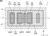
- the capacitor 1 shown in FIG. 1 and FIG. 2 includes a substrate 10, an insulating film 21 provided on the substrate 10, two first electrodes 22 provided on the insulating film 21, a first dielectric film 23 provided on the two first electrodes, three second electrodes 24 provided on the two first electrodes 22 via the first dielectric film 23, a moisture-resistant film 25 provided on the first dielectric film 23 and the second electrode 24, a first protective layer 26 covering the two first electrodes 22, the three second electrodes 24, and the moisture-resistant film 25, three external electrodes 27 penetrating the first protective layer 26, and a second protective layer 29 covering one of the three external electrodes 27 except for the two external electrodes 27.
- the second electrode 24 includes second electrodes 24A and 24B provided on the first electrode 22A, and a second electrode 24C provided on the first electrode 22B.
- At least one second electrode 24 is disposed on each first electrode 22, and three capacitor elements CAP1, CAP2, and CAP3 are formed from two first electrodes 22, a first dielectric film 23, and three second electrodes 24.
- the three capacitor elements CAP1, CAP2, and CAP3 are electrically connected in series (see FIG. 3).
- two capacitor elements CAP1 and CAP2 having two second electrodes 24A and 24B disposed on the same first electrode 22A are electrically connected in series with their first electrodes 22A, and two capacitor elements CAP1 and CAP2 that are not covered with the second protective layer 29 are electrically connected in series with their first electrodes 22A.
- the two external electrodes 27 constitute two terminal electrodes 27A and 27B electrically connected to two of the three capacitor elements CAP1, CAP2, and CAP3, respectively.
- the two capacitor elements CAP2 and CAP3 having two second electrodes 24B and 24C arranged on different first electrodes 22A and 22B are electrically connected in series with the external electrode 27C that does not constitute the two terminal electrodes 27A and 27B, and the external electrode 27C that does not constitute the two terminal electrodes 27A and 27B is covered with a second protective layer 29.
- the capacitance generated by the variation in thickness of the dielectric film within the wafer surface is C0 ⁇ C0.
- the target capacitance C0/3 can be achieved whether the capacitances C1, C2, and C3 are the same value or a combination of different values.
- the capacitance variation reflecting the film thickness variation of the dielectric film differs for each capacitance, and when different capacitances C1, C2, and C3 are used, the total capacitance variation ⁇ C0/3 becomes large, so it is preferable that the capacitances C1, C2, and C3 are the same capacitance.
- Another effect is that by connecting multiple capacitor elements in series, it is easy to form a low-capacitance capacitor. For example, if one capacitor is formed on one chip with a dielectric film that is 1 ⁇ m thick, the capacitance will be 1 pF. On the other hand, with the above configuration, the electrode area is 1/4 and there are three capacitors in series, making it possible to form a low-capacitance capacitor with a capacitance of 0.1 pF or less.
- the two capacitor elements CAP2 and CAP3 formed by the different first electrodes 22A and 22B are not electrically connected in series to a common second electrode, but are electrically connected in series to the external electrode 27C that penetrates the first protective layer 26, so that it is possible to suppress interference between the capacitor elements CAP2 and CAP3. This interference can be particularly suppressed when the substrate 10 is a semiconductor substrate.
- the substrate 10 is not particularly limited, but is preferably a semiconductor substrate such as a silicon substrate or a gallium arsenide substrate, or an insulating substrate such as glass or alumina.
- the insulating film 21 is provided so as to cover the entirety of one of the main surfaces of the substrate 10.
- the insulating film 21 may be provided so as to cover a portion of one of the main surfaces of the substrate 10, but it must be provided in an area that is larger than the first electrode 22 and overlaps the entire area of the first electrode 22. Note that if the substrate 10 is an insulating substrate such as glass or alumina, the insulating film 21 does not need to be provided.
- the capacitor elements CAP1, CAP2, and CAP3 are electrically insulated from the semiconductor substrate. This makes it possible to reduce the parasitic capacitance components of each of the capacitor elements CAP1, CAP2, and CAP3.
- the material constituting the insulating film 21 is not particularly limited, but preferable examples include SiO2 , SiN, Al2O3 , HfO2 , Ta2O5 , and ZrO2 .
- the first electrode 22 is provided at a position away from the edge of the substrate 10. In other words, the edge of the first electrode 22 is located inside the edge of the substrate 10.
- the material constituting the first electrode 22 is not particularly limited, but is preferably Cu, Ag, Au, Al, Ni, Cr, or Ti, or an alloy containing at least one of these metals.
- the first dielectric film 23 is provided so as to cover the first electrode 22 except for the opening.
- the end of the first dielectric film 23 is also provided on the surface of the insulating film 21 from the end of the first electrode 22 to the end of the substrate 10. The end of the first dielectric film 23 does not have to be provided to the end of the substrate 10.
- the material constituting the first dielectric film 23 is not particularly limited, but preferably includes oxides or nitrides such as SiO2 , SiN , Al2O3 , HfO2 , and Ta2O5 .
- the second electrode 24 is disposed opposite the first electrode 22 with the first dielectric film 23 interposed therebetween. More specifically, the second electrodes 24A and 24B face the first electrode 22A, and the second electrode 24C faces the first electrode 22B.
- the three second electrodes 24 have the same area and the same planar shape. Specifically, the three second electrodes 24 have a rectangular shape with the same dimensions in the length direction L and width direction W.
- the material constituting the second electrode 24 is not particularly limited, but is preferably Cu, Ag, Au, Al, Ni, Cr, or Ti, or an alloy containing at least one of these metals.
- the moisture-resistant film 25 is provided so as to cover the first dielectric film 23 and the second electrode 24 except for the opening.
- the provision of the moisture-resistant film 25 enhances the moisture resistance of the capacitor element, particularly the first dielectric film 23. Note that the moisture-resistant film 25 does not necessarily have to be provided.
- the material constituting the moisture-resistant film 25 is not particularly limited, but preferably includes moisture-resistant materials such as SiO 2 and SiN.
- the first protective layer 26 has openings at positions overlapping the openings of the first dielectric film 23 and moisture-resistant film 25 (openings overlapping the first electrode 22B) and at a position overlapping the opening of the moisture-resistant film 25 (openings overlapping the second electrode 24).
- the provision of the first protective layer 26 protects the capacitor element, and in particular the first dielectric film 23, from moisture.
- the material constituting the first protective layer 26 is not particularly limited, but preferred examples include resin materials such as polyimide resin and resin in solder resist.
- the thickness of the first protective layer 26 is not particularly limited, but is preferably 0.5 ⁇ m or more and 10 ⁇ m or less, and more preferably 1 ⁇ m or more and 5 ⁇ m or less.
- the external electrodes 27 constituting the terminal electrodes 27A and 27B are each electrically connected to the capacitor elements (here, the capacitor elements CAP1 and CAP3) connected in series at both ends of the three capacitor elements CAP1, CAP2, and CAP3. More specifically, the external electrodes 27 constituting the terminal electrodes 27A and 27B are connected to the second electrode 24A and the first electrode 22B, respectively.
- the external electrode 27C which does not constitute the terminal electrodes 27A and 27B, is a connection wiring, and is electrically connected to the capacitor element (here, capacitor element CAP2) excluding the capacitor element connected in series at both ends of the three capacitor elements CAP1, CAP2, and CAP3, and to the other capacitor element (here, capacitor element CAP3). More specifically, the external electrode 27C is connected to the second electrodes 24B and 24C.
- the material constituting the external electrode 27 is not particularly limited, but preferably includes Cu, Ni, Ag, Au, Al, etc.
- the external electrode 27 may have a single-layer structure or a multi-layer structure.
- the outermost surface of the external electrode 27 is preferably made of Au or Sn.
- the external electrode 27 may have, in order from the substrate 10 side, a seed layer 28a, a first plating layer 28b, and a second plating layer 28c, as shown in FIG. 1.
- the seed layer 28a of the external electrode 27 may be, for example, a laminate (Ti/Cu) of a conductive layer made of titanium (Ti) and a conductive layer made of copper (Cu).
- Examples of the material for the first plating layer 28b of the external electrode 27 include nickel (Ni).
- Examples of materials that may be used for the second plating layer 28c of the external electrode 27 include gold (Au) and tin (Sn).
- the materials constituting the three external electrodes 27 may be the same as each other or different from each other.
- the second protective layer 29 has openings so that the terminal electrodes 27A, 27B are exposed.
- the second protective layer 29 insulates the external electrode 27 (external electrode 27C) excluding the terminal electrodes 27A and 27B from the outside. Furthermore, the provision of the second protective layer 29 makes it possible to more effectively protect the capacitor element, and in particular the first dielectric film 23, from moisture.
- the material constituting the second protective layer 29 is not particularly limited, but preferred examples include resin materials such as polyimide resin and resin in solder resist.
- the distance between adjacent capacitor elements is not particularly limited, but is preferably 5 ⁇ m or more and 100 ⁇ m or less, and more preferably 10 ⁇ m or more and 50 ⁇ m or less. By making it 100 ⁇ m or less, the difference in film thickness of the first dielectric film 23 between each capacitor element becomes small, and capacitor elements of the same capacitance can be formed.
- the capacitor 1 shown in Figures 1 and 2 is manufactured, for example, using a method similar to the manufacturing method of a typical MIM capacitor.
- the capacitor according to the second embodiment of the present invention differs from the first embodiment in that at least two of the three second electrodes have different areas.
- FIG. 4 is a cross-sectional view showing an example of a capacitor according to the second embodiment of the present invention.
- FIG. 5 is a plan view showing an example of a capacitor according to the second embodiment of the present invention.
- FIG. 4 is a cross-sectional view taken along line I-I of the capacitor shown in FIG. 5.
- FIG. 6 shows an equivalent circuit of the capacitor shown in FIGS. 4 and 5.
- the capacitor 1 shown in Figures 1 and 2 can reduce capacitance variation, but there is a possibility that the center of capacitance may deviate from the desired value.
- At least two of the three second electrodes 24 have different areas. This makes it possible to adjust the capacitance center. This is because the area of each second electrode 24 can be set so as to cancel out the film thickness distribution of the first dielectric film 23 within the wafer surface.
- each second electrode 24 is composed of a first region 30a having a rectangular planar shape and a second region 30b having a rectangular planar shape protruding from the first region 30a.
- the areas of the first regions 30a of the three second electrodes 24 are the same, while the areas of the second regions 30b of at least two of the three second electrodes 24 are different from each other.
- the areas of all the second electrodes 24 may be different from each other, and the areas of the second regions 30b of all the second electrodes 24 may be different from each other.
- the capacitor 2 shown in Figures 4 and 5 is manufactured using, for example, the method described in Patent Document 2.
- the capacitance center can be adjusted to a desired value.
- the area of the second electrode 24 can be corrected to cancel the film thickness distribution of the first dielectric film 23 within the wafer surface, making it possible to reduce the capacitance distribution. In other words, a capacitor with an adjusted capacitance center and reduced capacitance variation can be realized.
- FIG. 7 is a cross-sectional view showing an example of a capacitor according to the third embodiment of the present invention.
- FIG. 8 is a plan view showing an example of a capacitor according to the third embodiment of the present invention.
- FIG. 7 is a cross-sectional view taken along line I-I of the capacitor shown in FIG. 8.
- FIG. 9 shows an equivalent circuit of the capacitor shown in FIGS. 7 and 8.
- the capacitor 3 shown in Figures 7 and 8 further includes a second dielectric film 31 provided on the three second electrodes 24, and three third electrodes 32 provided on the three second electrodes 24, respectively, via the second dielectric film 31.
- three capacitor elements CAP4, CAP5, and CAP6 are composed of three second electrodes 24, a second dielectric film 31, and three third electrodes 32, and the six capacitor elements CAP1 to CAP6 are electrically connected in series (see Figure 9).
- the number of series connections can be increased, and capacitance variation can be further suppressed.
- the capacitor elements are formed in the thickness direction, the chip can be made smaller.
- At least two of the three third electrodes 32 have different areas. This makes it possible to adjust the center of capacitance. This is because the area of each third electrode 32 can be set so as to cancel out the film thickness distribution of the second dielectric film 31 within the wafer surface.
- each third electrode 32 is composed of a first region 33a having a rectangular planar shape and a second region 33b having a rectangular planar shape protruding from the first region 33a.
- the areas of the first regions 33a of the three third electrodes 32 are the same, while the areas of the second regions 33b of at least two of the three third electrodes 32 are different from each other.
- the areas of all the third electrodes 32 may be different from each other, and the areas of the second regions 33b of all the third electrodes 32 may be different from each other.
- FIG. 8 shows a state in which each third electrode 32 overlaps exactly with the opposing second electrode 24 when viewed from a plane in the thickness direction T, but each third electrode 32 may partially overlap with the opposing second electrode 24 when viewed from a plane in the thickness direction T. Also, each third electrode 32 may be formed within the frame of each second electrode 24.
- the capacitor 3 shown in Figures 7 and 8 is manufactured using, for example, the method described in Patent Document 2.
- the second dielectric film 31 is provided so as to cover the second electrode 24 except for the opening.
- the end of the second dielectric film 31 is also provided on the surface of the first dielectric film 23 between the end of the first electrode 22 and the first dielectric film 23.
- the end of the second dielectric film 31 does not have to be provided to the end of the substrate 10.
- the material constituting the second dielectric film 31 is not particularly limited , but preferably includes oxides or nitrides such as SiO2 , SiN, Al2O3 , HfO2 , and Ta2O5 .
- the third electrode 32 is disposed opposite the second electrode 24 with the second dielectric film 31 interposed therebetween. More specifically, the third electrode 32 includes a third electrode 32A opposite the second electrode 24A, a third electrode 32B opposite the second electrode 24B, and a third electrode 32C opposite the second electrode 24C.
- the material constituting the third electrode 32 is not particularly limited, but is preferably Cu, Ag, Au, Al, Ni, Cr, or Ti, or an alloy containing at least one of these metals.
- the external electrodes 27 constituting the terminal electrodes 27A and 27B are each electrically connected to one of the six capacitor elements CAP1 to CAP6 (capacitor elements CAP4 and CAP3 in this example) that are connected in series to both ends. More specifically, the external electrodes 27 constituting the terminal electrodes 27A and 27B are each connected to the third electrode 32A and the first electrode 22B.
- the external electrode 27C which does not constitute the terminal electrodes 27A and 27B, is electrically connected to two of the six capacitor elements CAP1 to CAP6 (here, the capacitor elements CAP5 and CAP6) excluding the capacitor elements connected in series at both ends. More specifically, the external electrode 27C is connected to the third electrodes 32B and 32C.
- FIG. 10 is a cross-sectional view showing an example of a capacitor according to the fourth embodiment of the present invention.
- FIG. 11 is a plan view showing an example of a capacitor according to the fourth embodiment of the present invention.
- FIG. 10 is a cross-sectional view taken along line II of the capacitor shown in FIG. 11.
- FIG. 12 shows an equivalent circuit of the capacitor shown in FIGS. 10 and 11.
- the capacitor 4 shown in Figures 10 and 11 further includes a third dielectric film 34 provided on the three third electrodes 32, and three fourth electrodes 35 provided on the three third electrodes 32, respectively, via the third dielectric film 34.
- three capacitor elements CAP7, CAP8, and CAP9 are composed of three third electrodes 32, a third dielectric film 34, and three fourth electrodes 35, and the nine capacitor elements CAP1 to CAP9 are electrically connected in series (see FIG. 12).
- the number of series connections can be increased, and capacitance variation can be further suppressed.
- the capacitor elements are formed in the thickness direction, the chip can be made smaller.
- At least two of the three fourth electrodes 35 have different areas. This makes it possible to adjust the capacitance center. This is because the area of each fourth electrode 35 can be set so as to cancel out the film thickness distribution of the third dielectric film 34 within the wafer surface.
- each fourth electrode 35 is composed of a first region 36a having a rectangular planar shape and a second region 36b having a rectangular planar shape protruding from the first region 36a.
- the areas of the first regions 36a of the three fourth electrodes 35 are the same, while the areas of the second regions 36b of at least two of the three fourth electrodes 35 are different from each other.
- the areas of all the fourth electrodes 35 may be different from each other, and the areas of the second regions 36b of all the fourth electrodes 35 may be different from each other.
- FIG. 11 shows a state in which each fourth electrode 35 overlaps the opposing third electrode 32 perfectly, but in plan view from the thickness direction T, each fourth electrode 35 may partially overlap the opposing third electrode 32. Also, in plan view from the thickness direction T, FIG. 11 shows a state in which each third electrode 32 overlaps the opposing second electrode 24 perfectly, but in plan view from the thickness direction T, each third electrode 32 may partially overlap the opposing second electrode 24. Also, each fourth electrode 35 may be formed within the frame of each third electrode 32, and each third electrode 32 may be formed within the frame of each second electrode 24.
- the capacitor 4 shown in Figures 10 and 11 is manufactured using, for example, the method described in Patent Document 2.
- the third dielectric film 34 is provided so as to cover the third electrode 32 except for the opening.
- the end of the third dielectric film 34 is also provided on the surface of the second dielectric film 31 between the end of the first electrode 22 and the second dielectric film 31.
- the end of the third dielectric film 34 does not have to be provided to the end of the substrate 10.
- the material constituting the third dielectric film 34 is not particularly limited, but preferably includes oxides or nitrides such as SiO2 , SiN, Al2O3 , HfO2 , and Ta2O5 .
- the fourth electrode 35 is disposed opposite the third electrode 32 with the third dielectric film 34 interposed therebetween. More specifically, the fourth electrode 35 includes a fourth electrode 35A opposite the third electrode 32A, a fourth electrode 35B opposite the third electrode 32B, and a fourth electrode 35C opposite the third electrode 32C.
- the material constituting the fourth electrode 35 is not particularly limited, but is preferably Cu, Ag, Au, Al, Ni, Cr, or Ti, or an alloy containing at least one of these metals.
- the external electrodes 27 constituting the terminal electrodes 27A and 27B are each electrically connected to the capacitor elements (here, the capacitor elements CAP7 and CAP3) connected in series to both ends of the nine capacitor elements CAP1 to CAP9. More specifically, the external electrodes 27 constituting the terminal electrodes 27A and 27B are connected to the fourth electrode 35A and the first electrode 22B, respectively.
- the external electrode 27C which does not constitute the terminal electrodes 27A and 27B, is electrically connected to two of the nine capacitor elements CAP1 to CAP9 (here, capacitor elements CAP8 and CAP9) excluding the capacitor elements connected in series at both ends. More specifically, the external electrode 27C is connected to the fourth electrodes 35B and 35C.
- the capacitor according to the fifth embodiment of the present invention differs from the second embodiment in that an element isolation is provided between three capacitor elements within a semiconductor substrate.
- FIG. 13 is a cross-sectional view showing an example of a capacitor according to the fifth embodiment of the present invention.
- FIG. 14 is a plan view showing an example of a capacitor according to the fifth embodiment of the present invention.
- FIG. 13 is a cross-sectional view taken along line II of the capacitor shown in FIG. 14.
- FIG. 15 shows an equivalent circuit of the capacitor shown in FIGS. 13 and 14.
- the substrate 10 is a semiconductor substrate, and element isolation 37 is provided in the semiconductor substrate between the three capacitor elements CAP1, CAP2, and CAP3.
- the element isolation 37 has a structure in which a cavity is formed in a semiconductor substrate and an SiO 2 film is embedded therein (STI: Shallow Trench Isolation).
- STI Shallow Trench Isolation
- the element isolation 37 is provided at least between adjacent capacitor elements (here, between capacitor elements CAP1 and CAP2 and between capacitor elements CAP2 and CAP3), and is preferably provided so as to surround each of the capacitor elements CAP1, CAP2, and CAP3. Furthermore, the element isolation 37 is preferably arranged so as to overlap the peripheral portion of the first electrode 22 and border the peripheral portion.
- the capacitor according to the sixth embodiment of the present invention differs from the fifth embodiment in that the material for element isolation is different.
- FIG. 16 is a cross-sectional view showing an example of a capacitor according to the sixth embodiment of the present invention.
- FIG. 17 is a plan view showing an example of a capacitor according to the sixth embodiment of the present invention.
- FIG. 16 is a cross-sectional view taken along line II of the capacitor shown in FIG. 17.
- FIG. 18 shows an equivalent circuit of the capacitor shown in FIGS. 16 and 17.
- the substrate 10 is an n-type semiconductor substrate
- the element isolation 37 has a structure in which a p+ active layer is formed in an n-type semiconductor substrate.
- Such element isolation 37 can be formed, for example, by injecting a high concentration of p-type impurities into an n-type semiconductor substrate by ion implantation.
- This embodiment also reduces the current flowing through the semiconductor substrate between adjacent capacitor elements, making it possible to reduce the mutual interference between adjacent capacitor elements. As a result, the accuracy of the center capacitance value and capacitance variation of the capacitor 6 can be improved.
- the semiconductor device of the present invention is not limited to the above-described embodiment, and various applications and modifications can be made within the scope of the present invention with respect to the configuration and manufacturing conditions of the semiconductor device such as a capacitor.
- a fourth second electrode may be provided on the first electrode 22B via the first dielectric film 23, and the terminal electrode 27B may be connected to the second electrode.
- a fourth second electrode may be provided on the first electrode 22B via the first dielectric film 23, and a fourth third electrode may be provided on the second electrode via the second dielectric film 31, and the terminal electrode 27B may be connected to the third electrode.
- a fourth second electrode may be provided on the first electrode 22B via the first dielectric film 23
- a fourth third electrode may be provided on the second electrode via the second dielectric film 31
- a fourth fourth electrode may be provided on the third electrode via the third dielectric film 34
- the terminal electrode 27B may be connected to the fourth electrode.
- N is not particularly limited as long as it is an integer of 2 or more, and may be, for example, 3.
- a third first electrode is provided between the two first electrodes 22A and 22B, and a fourth and fifth second electrode is provided on the first electrode via the first dielectric film 23 to form a fourth and fifth capacitor element (a total of five capacitor elements connected in series), and the fourth capacitor element and capacitor element CAP2 are electrically connected in series with external electrodes that do not constitute the terminal electrodes 27A and 27B, and the fifth capacitor element and capacitor element CAP3 are electrically connected in series with external electrodes that do not constitute the terminal electrodes 27A and 27B.
- N first electrodes (where N is an integer of 2 or more) provided on the substrate; a first dielectric film provided on the N first electrodes; M second electrodes (where M is an integer of 3 or more satisfying M>N) provided on the N first electrodes via the first dielectric film; a first protective layer covering the N first electrodes and the M second electrodes; Three or more external electrodes penetrating the first protective layer; a second protective layer that covers the external electrodes excluding two of the three or more external electrodes; At least one second electrode is disposed on each of the first electrodes; the N first electrodes, the first dielectric film, and the M second electrodes constitute M capacitor elements; The M capacitor elements are electrically connected in series, Among the M capacitor elements, two capacitor elements having two second electrodes arranged on the same first electrode are electrically connected in series at their first electrodes; the two external electrodes not covered with the second protective layer constitute two terminal electrodes electrically connected to two of the M capacitor elements, respectively; Among the M capacitor elements, two capacitor elements each
- ⁇ 2> The semiconductor device according to ⁇ 1>, wherein at least two of the M second electrodes have areas different from each other.
- ⁇ 3> a second dielectric film provided on the M second electrodes;
- ⁇ 4> The semiconductor device according to ⁇ 3>, wherein at least two of the M third electrodes have areas different from each other.
- ⁇ 5> a third dielectric film provided on the M third electrodes;
- ⁇ 6> 6 The semiconductor device according to claim 5, wherein at least two of said M fourth electrodes have areas different from each other.
- the substrate is a semiconductor substrate
Landscapes
- Engineering & Computer Science (AREA)
- Power Engineering (AREA)
- Microelectronics & Electronic Packaging (AREA)
- Manufacturing & Machinery (AREA)
- Semiconductor Integrated Circuits (AREA)
Abstract
Description
本発明は、半導体装置に関する。 The present invention relates to a semiconductor device.
半導体集積回路に用いられる代表的なキャパシタ素子として、例えばMIM(Metal Insulator Metal)キャパシタが知られている。MIMキャパシタは、絶縁体を下部電極と上部電極とで挟んだ平行平板型の構造を有するキャパシタである。 A typical capacitor element used in semiconductor integrated circuits is, for example, the MIM (Metal Insulator Metal) capacitor. The MIM capacitor is a capacitor with a parallel plate structure in which an insulator is sandwiched between a lower electrode and an upper electrode.
特許文献1には、共通ポートと、第1の信号ポートと、第2の信号ポートと、上記共通ポートと上記第1の信号ポートとの間に設けられ、第1の遮断周波数以下の第1の通過帯域内の周波数の信号を選択的に通過させるローパスフィルタと、上記共通ポートと上記第2の信号ポートとの間に設けられ、上記第1の遮断周波数よりも高い第2の遮断周波数以上の第2の通過帯域内の周波数の信号を選択的に通過させるハイパスフィルタとを備えた分波器であって、上記ローパスフィルタは、第1のLC共振回路と、上記第1のLC共振回路から上記第1の信号ポートに至る経路とグランドとを接続する分路に設けられた第1の弾性波共振器とを含み、上記第1の弾性波共振器の共振周波数は、上記第1の遮断周波数よりも高いことを特徴とする分波器が開示されている。
特許文献2には、ウエハに誘電膜を形成するステップと、上記ウエハにおいて、上記誘電膜が形成された領域のうちの一部の領域に含まれるモニター領域において、上記ウエハに対向する面の面積が所定の面積であるモニター電極を形成するステップと、上記モニター領域に形成された上記モニター電極及び上記誘電膜によって形成される容量の容量値を測定するステップと、測定された上記容量値に基づいて、上記一部の領域のうち、上記モニター領域以外の領域であるキャパシタ形成領域において形成される上部電極の面積を算出するステップと、算出された上記面積に基づいて、上記キャパシタ形成領域に上記上部電極を形成するステップと、を含むキャパシタ製造方法が開示されている。
通信用RFモジュールにおける高周波回路において、700MHz以上の高周波が使用されている。通信速度を上げるために、今後3GHz以上の高周波が使用される。 High frequencies of 700 MHz and above are used in the high frequency circuits of RF modules for communication. In the future, high frequencies of 3 GHz and above will be used to increase communication speeds.
図19は、比較形態に係るフィルタ回路を示す回路図である。 FIG. 19 is a circuit diagram showing a filter circuit according to a comparative example.
例えば、所望の周波数を回路の後段に伝達しないフィルタ回路は、特許文献1の図1や図19のようにして実現される。LとCを直列接続し、共振周波数f0=1/2π√(LC)の信号をグランドに落としている。
For example, a filter circuit that does not transmit the desired frequency to the subsequent stages of the circuit can be realized as shown in Fig. 1 and Fig. 19 of
高周波になるほど、LやCの定数のばらつきが共振周波数に及ぼす影響が大きくなるため、高周波回路にはばらつきが最も狭い規格偏差の部品が選定されていた。 The higher the frequency, the greater the effect that variations in the L and C constants have on the resonant frequency, so components with the narrowest standard deviations were selected for high-frequency circuits.
例として、図19のLCフィルタ回路において、L=1nH、C=1pFの場合、f0=5.03GHzであるが、Cが±0.05pFの容量偏差であると仮定し、C=0.95~1.05pFに変動する場合、f0は4.91~5.16GHzに変動する。高周波回路のフィルタ特性として、上記の共振周波数f0の変動量は致命的となる場合がある。 For example, in the LC filter circuit of Figure 19, when L = 1nH and C = 1pF, f0 = 5.03GHz, but if we assume that C has a capacitance deviation of ±0.05pF and C varies from 0.95 to 1.05pF, f0 will vary from 4.91 to 5.16GHz. As a filter characteristic of a high-frequency circuit, the above fluctuation in the resonant frequency f0 can be fatal.
上記の問題を解決するために、CやLの偏差がより狭い部品を選定することが考えられる。しかしながら、従来の電子部品では、偏差に最小値の限界があり、対応できない場合がある。 To solve the above problem, it is possible to select components with narrower C and L deviations. However, with conventional electronic components, there is a minimum limit to the deviation, and this may not be possible.
本発明は、上記の問題を解決するためになされたものであり、容量偏差の小さい半導体装置を提供することを目的とする。 The present invention was made to solve the above problems, and aims to provide a semiconductor device with small capacitance deviation.
本発明の半導体装置は、基板と、上記基板上に設けられたN個(ただし、Nは2以上の整数)の第1の電極と、上記N個の第1の電極上に設けられた第1の誘電体膜と、上記第1の誘電体膜を介して、上記N個の第1の電極上に設けられたM個(ただし、MはM>Nを満たす3以上の整数)の第2の電極と、上記N個の第1の電極及び上記M個の第2の電極を覆う第1の保護層と、上記第1の保護層を貫通する3個以上の外部電極と、上記3個以上の外部電極のうち、2つの外部電極を除く外部電極を覆う第2の保護層と、を備え、上記各第1の電極上には少なくとも1つの第2の電極が配置され、上記N個の第1の電極と、上記第1の誘電体膜と、上記M個の第2の電極とから、M個のキャパシタ素子が構成されており、上記M個のキャパシタ素子は、電気的に直列接続されており、上記M個のキャパシタ素子のうち、同じ第1の電極上に配置された2つの第2の電極を有する2つのキャパシタ素子は、その第1の電極で電気的に直列接続されており、上記第2の保護層で覆われていない上記2つの外部電極は、上記M個のキャパシタ素子のうちの2つのキャパシタ素子にそれぞれ電気的に接続された2つの端子電極を構成し、上記M個のキャパシタ素子のうち、異なる第1の電極上に配置された2つの第2の電極を有する2つのキャパシタ素子は、上記2つの端子電極を構成しない外部電極で電気的に直列接続されており、上記2つの端子電極を構成しない上記外部電極は、上記第2の保護層で覆われている。 The semiconductor device of the present invention comprises a substrate, N first electrodes (where N is an integer of 2 or more) provided on the substrate, a first dielectric film provided on the N first electrodes, M second electrodes (where M is an integer of 3 or more satisfying M>N) provided on the N first electrodes via the first dielectric film, a first protective layer covering the N first electrodes and the M second electrodes, three or more external electrodes penetrating the first protective layer, and a second protective layer covering the external electrodes excluding two of the three or more external electrodes, at least one second electrode being disposed on each of the first electrodes, and M capacitor elements being formed from the N first electrodes, the first dielectric film, and the M second electrodes. The M capacitor elements are electrically connected in series, and among the M capacitor elements, two capacitor elements having two second electrodes arranged on the same first electrode are electrically connected in series with their first electrodes, and the two external electrodes not covered with the second protective layer constitute two terminal electrodes electrically connected to two of the M capacitor elements, respectively, and among the M capacitor elements, two capacitor elements having two second electrodes arranged on different first electrodes are electrically connected in series with external electrodes that do not constitute the two terminal electrodes, and the external electrodes that do not constitute the two terminal electrodes are covered with the second protective layer.
本発明によれば、容量偏差の小さい半導体装置を提供することができる。 The present invention makes it possible to provide a semiconductor device with small capacitance deviation.
以下、本発明の半導体装置について説明する。
しかしながら、本発明は、以下の構成に限定されるものではなく、本発明の要旨を変更しない範囲において適宜変更して適用することができる。なお、以下において記載する本発明の個々の好ましい構成を2つ以上組み合わせたものもまた本発明である。
The semiconductor device of the present invention will now be described.
However, the present invention is not limited to the following configurations, and can be appropriately modified and applied within the scope of the present invention. Note that the present invention also includes a combination of two or more of the individual preferred configurations of the present invention described below.
以下に示す各実施形態は例示であり、異なる実施形態で示した構成の部分的な置換又は組み合わせが可能であることは言うまでもない。第2実施形態以降では、第1実施形態と共通の事項についても記述は省略し、異なる点についてのみ説明する。特に、同様の構成による同様の作用効果については、実施形態毎に逐次言及しない。 The embodiments shown below are merely examples, and it goes without saying that partial substitution or combination of the configurations shown in different embodiments is possible. From the second embodiment onwards, descriptions of matters common to the first embodiment will be omitted, and only the differences will be explained. In particular, similar effects resulting from similar configurations will not be mentioned one by one for each embodiment.
以下の説明において、各実施形態を特に区別しない場合、単に「本発明の半導体装置」と言う。本発明の半導体装置及び各構成要素の形状及び配置等は、図示する例に限定されるものではない。 In the following description, unless otherwise specified, each embodiment will be referred to simply as the "semiconductor device of the present invention." The shape and arrangement of each component of the semiconductor device of the present invention are not limited to the examples shown in the drawings.
また、以下においては、本発明の半導体装置の一実施形態として、キャパシタを例にとって説明する。本発明の半導体装置は、キャパシタそのものであってもよく、キャパシタを含む装置であってもよい。 Below, a capacitor will be used as an example of one embodiment of the semiconductor device of the present invention. The semiconductor device of the present invention may be a capacitor itself, or may be a device that includes a capacitor.
本発明の半導体装置は、基板と、上記基板上に設けられたN個(ただし、Nは2以上の整数)の第1の電極と、上記N個の第1の電極上に設けられた第1の誘電体膜と、上記第1の誘電体膜を介して、上記N個の第1の電極上に設けられたM個(ただし、MはM>Nを満たす3以上の整数)の第2の電極と、上記N個の第1の電極及び上記M個の第2の電極を覆う第1の保護層と、上記第1の保護層を貫通する3個以上の外部電極と、上記3個以上の外部電極のうち、2つの外部電極を除く外部電極を覆う第2の保護層と、を備え、上記各第1の電極上には少なくとも1つの第2の電極が配置され、上記N個の第1の電極と、上記第1の誘電体膜と、上記M個の第2の電極とから、M個のキャパシタ素子が構成されており、上記M個のキャパシタ素子は、電気的に直列接続されており、上記M個のキャパシタ素子のうち、同じ第1の電極上に配置された2つの第2の電極を有する2つのキャパシタ素子は、その第1の電極で電気的に直列接続されており、上記第2の保護層で覆われていない上記2つの外部電極は、上記M個のキャパシタ素子のうちの2つのキャパシタ素子にそれぞれ電気的に接続された2つの端子電極を構成し、上記M個のキャパシタ素子のうち、異なる第1の電極上に配置された2つの第2の電極を有する2つのキャパシタ素子は、上記2つの端子電極を構成しない外部電極で電気的に直列接続されており、上記2つの端子電極を構成しない上記外部電極は、上記第2の保護層で覆われていることを特徴とする。 The semiconductor device of the present invention comprises a substrate, N first electrodes (where N is an integer of 2 or more) provided on the substrate, a first dielectric film provided on the N first electrodes, M second electrodes (where M is an integer of 3 or more satisfying M>N) provided on the N first electrodes via the first dielectric film, a first protective layer covering the N first electrodes and the M second electrodes, three or more external electrodes penetrating the first protective layer, and a second protective layer covering the external electrodes excluding two of the three or more external electrodes, at least one second electrode being disposed on each of the first electrodes, and M capacitor elements being constituted by the N first electrodes, the first dielectric film, and the M second electrodes. The M capacitor elements are electrically connected in series, and among the M capacitor elements, two capacitor elements having two second electrodes arranged on the same first electrode are electrically connected in series with their first electrodes, and the two external electrodes that are not covered with the second protective layer constitute two terminal electrodes that are electrically connected to two of the M capacitor elements, respectively, and among the M capacitor elements, two capacitor elements having two second electrodes arranged on different first electrodes are electrically connected in series with external electrodes that do not constitute the two terminal electrodes, and the external electrodes that do not constitute the two terminal electrodes are covered with the second protective layer.
なお、本明細書中、「第1、第2、第3、第4、・・・の電極」とは、キャパシタ素子を形成する電極のうち、基板側から数えて、それぞれ、1層目(1番目)、2層目(2番目)、3層目(3番目)、4層目(4番目)、・・・に存在する電極を意味する。 In this specification, the terms "first, second, third, fourth, ... electrodes" refer to the electrodes that are present in the first layer (first), second layer (second), third layer (third), fourth layer (fourth), ... of the electrodes that form the capacitor element, counting from the substrate side.
また、本明細書中、「キャパシタ素子」とは、誘電体膜と、その誘電体膜を介して対向する一対の電極とによって構成される素子(小キャパシタ)を意味し、「キャパシタ」とは、複数のキャパシタ素子を含む概念を表す。 In addition, in this specification, "capacitor element" refers to an element (small capacitor) composed of a dielectric film and a pair of electrodes facing each other through the dielectric film, and "capacitor" refers to the concept of including multiple capacitor elements.
[第1実施形態]
本発明の第1実施形態に係るキャパシタは、2個(すなわちN=2)の第1の電極と、3個(すなわちM=3)の第2の電極と、3個の外部電極と、を備えている。
[First embodiment]
The capacitor according to the first embodiment of the present invention has two (ie, N=2) first electrodes, three (ie, M=3) second electrodes, and three external electrodes.
図1は、本発明の第1実施形態に係るキャパシタの一例を模式的に示す断面図である。図2は、本発明の第1実施形態に係るキャパシタの一例を模式的に示す平面図である。図1は、図2に示すキャパシタのI-I線に沿った断面図である。図3は、図1及び図2に示すキャパシタの等価回路を示す。 FIG. 1 is a cross-sectional view showing an example of a capacitor according to a first embodiment of the present invention. FIG. 2 is a plan view showing an example of a capacitor according to a first embodiment of the present invention. FIG. 1 is a cross-sectional view taken along line II of the capacitor shown in FIG. 2. FIG. 3 shows an equivalent circuit of the capacitor shown in FIG. 1 and FIG. 2.
本明細書中、キャパシタ(半導体装置)の長さ方向、幅方向、及び、厚み方向を、図1及び図2等に示すように、各々、矢印L、矢印W、及び、矢印Tで定められる方向とする。ここで、長さ方向Lと幅方向Wと厚み方向Tとは、互いに直交している。 In this specification, the length direction, width direction, and thickness direction of a capacitor (semiconductor device) are defined as the directions indicated by arrows L, W, and T, respectively, as shown in Figures 1 and 2. Here, the length direction L, width direction W, and thickness direction T are mutually orthogonal.
図1及び図2に示すキャパシタ1は、基板10と、基板10上に設けられた絶縁膜21と、絶縁膜21上に設けられた2個の第1の電極22と、2個の第1の電極上に設けられた第1の誘電体膜23と、第1の誘電体膜23を介して、2個の第1の電極22上に設けられた3個の第2の電極24と、第1の誘電体膜23及び第2の電極24上に設けられた耐湿膜25と、2個の第1の電極22、3個の第2の電極24及び耐湿膜25を覆う第1の保護層26と、第1の保護層26を貫通する3個の外部電極27と、3個の外部電極27のうち、2つの外部電極27を除く1つの外部電極27を覆う第2の保護層29と、を備えている。
The
2個の第1の電極22の一方を第1の電極22Aとし、他方を第1の電極22Bとすると、第2の電極24は、第1の電極22A上に設けられた第2の電極24A及び24Bと、第1の電極22B上に設けられた第2の電極24Cと、を含んでいる。
If one of the two
そして、各第1の電極22上には少なくとも1つの第2の電極24が配置され、2個の第1の電極22と、第1の誘電体膜23と、3個の第2の電極24とから、3個のキャパシタ素子CAP1、CAP2及びCAP3が構成されており、3個のキャパシタ素子CAP1、CAP2及びCAP3は、電気的に直列接続されており(図3参照)、3個のキャパシタ素子CAP1、CAP2及びCAP3のうち、同じ第1の電極22A上に配置された2つの第2の電極24A及び24Bを有する2つのキャパシタ素子CAP1及びCAP2は、その第1の電極22Aで電気的に直列接続されており、第2の保護層29で覆われていない2つの外部電極27は、3個のキャパシタ素子CAP1、CAP2及びCAP3のうちの2つのキャパシタ素子CAP1及びCAP3にそれぞれ電気的に接続された2つの端子電極27A及び27Bを構成し、3個のキャパシタ素子CAP1、CAP2及びCAP3のうち、異なる第1の電極22A及び22B上に配置された2つの第2の電極24B及び24Cを有する2つのキャパシタ素子CAP2及びCAP3は、2つの端子電極27A及び27Bを構成しない外部電極27Cで電気的に直列接続されており、2つの端子電極27A及び27Bを構成しない外部電極27Cは、第2の保護層29で覆われていることを特徴としている。
At least one
これにより、容量偏差(容量ばらつき)の小さいキャパシタを作製することができる。以下、その理由を説明する。 This makes it possible to create capacitors with small capacitance deviations (capacity variations). The reasons for this are explained below.
ウエハ面内の誘電体膜の膜厚ばらつきによって、発生する容量がC0±ΔC0であると仮定する。上記3直列キャパシタ素子の構成を取ることによって実現することができる容量は、キャパシタ素子CAP1、CAP2及びCAP3の容量をそれぞれC1、C2及びC3とすると、1/C=1/C1+1/C2+1/C3から計算され、C0/3+ΔC0/3となる。つまり、3直列接続することによって、容量偏差を1/3に低減することができる。
Assume that the capacitance generated by the variation in thickness of the dielectric film within the wafer surface is C0±ΔC0. The capacitance that can be achieved by adopting the above configuration of three series capacitor elements is calculated as 1/C=1/
容量狙い値C0/3は、容量C1、C2及びC3が同じ値であっても、異なる値の組み合わせであっても実現することができる。しかしながら、誘電体膜の膜厚ばらつきを反映した容量ばらつきは容量ごとに異なり、異なる容量C1、C2及びC3を使う場合、合計の容量ばらつきΔC0/3が大きくなるため、容量C1、C2及びC3は同じ容量である方が好ましい。 The target capacitance C0/3 can be achieved whether the capacitances C1, C2, and C3 are the same value or a combination of different values. However, the capacitance variation reflecting the film thickness variation of the dielectric film differs for each capacitance, and when different capacitances C1, C2, and C3 are used, the total capacitance variation ΔC0/3 becomes large, so it is preferable that the capacitances C1, C2, and C3 are the same capacitance.
なお、本明細書中、ある量が同じであるとは、その量が実質的に同じ場合を含むものとする。 In this specification, when a certain amount is said to be the same, it is meant to include cases where the amount is substantially the same.
また別の効果として、複数のキャパシタ素子が直列接続されることによって、低容量のキャパシタを容易に形成することができる。例えば、膜厚1μmの誘電体膜に対して、1チップに1つのキャパシタを形成する場合、容量は1pFとなる。一方、上記構成をとる場合、電極面積は1/4となり、3直列であるため、容量0.1pF以下の低容量キャパシタを形成することができる。 Another effect is that by connecting multiple capacitor elements in series, it is easy to form a low-capacitance capacitor. For example, if one capacitor is formed on one chip with a dielectric film that is 1 μm thick, the capacitance will be 1 pF. On the other hand, with the above configuration, the electrode area is 1/4 and there are three capacitors in series, making it possible to form a low-capacitance capacitor with a capacitance of 0.1 pF or less.
更に、異なる第1の電極22A及び22Bによって形成された2つのキャパシタ素子CAP2及びCAP3が、共通の第2の電極で電気的に直列接続されるのではなく、第1の保護層26を貫通する外部電極27Cで電気的に直列接続されていることから、キャパシタ素子CAP2及びCAP3同士の干渉を抑制することが可能である。基板10が半導体基板である場合に、特にこの干渉を抑制することができる。
Furthermore, the two capacitor elements CAP2 and CAP3 formed by the different
以下、各構成について詳述する。 Each component is described in detail below.
基板10は、特に限定されないが、好ましくは、シリコン基板又はガリウム砒素基板等の半導体基板、あるいは、ガラス又はアルミナ等の絶縁性基板である。
The
絶縁膜21は、基板10の一方主面の全体を覆うように設けられている。絶縁膜21は、基板10の一方主面の一部を覆うように設けられていてもよいが、第1の電極22よりも大きく、かつ、第1の電極22の全域に重なる領域に設けられる必要がある。なお、基板10がガラス又はアルミナ等の絶縁性基板である場合には、絶縁膜21は設けられていなくてもよい。
The insulating
すなわち、絶縁膜21を設けることで、キャパシタ素子CAP1、CAP2及びCAP3と、半導体基板とを電気的に絶縁している。これにより、各々のキャパシタ素子CAP1、CAP2、CAP3の寄生容量成分を低減することができる。
In other words, by providing the insulating
絶縁膜21を構成する材料は、特に限定されないが、好ましくは、SiO2、SiN、Al2O3、HfO2、Ta2O5、ZrO2等が挙げられる。
The material constituting the insulating
第1の電極22は、基板10の端部と離れた位置に設けられている。すなわち、第1の電極22の端部は、基板10の端部よりも内側に位置している。
The
第1の電極22を構成する材料は、特に限定されないが、好ましくは、Cu、Ag、Au、Al、Ni、CrもしくはTi又はこれらの金属を少なくとも1種含む合金等が挙げられる。
The material constituting the
第1の誘電体膜23は、開口を除く部分で第1の電極22を覆うように設けられている。図1では、第1の誘電体膜23の端部は、第1の電極22の端部から基板10の端部までの絶縁膜21の表面上にも設けられている。第1の誘電体膜23の端部は、基板10の端部まで設けられていなくてもよい。
The
第1の誘電体膜23を構成する材料は、特に限定されないが、好ましくは、SiO2、SiN、Al2O3、HfO2、Ta2O5等の酸化物又は窒化物が挙げられる。
The material constituting the
第2の電極24は、第1の誘電体膜23を挟んで第1の電極22に対向して設けられている。より詳細には、第2の電極24A及び24Bは、第1の電極22Aに対向し、第2の電極24Cは、第1の電極22Bに対向している。
The
本実施形態では、図2に示すように、3個の第2の電極24の面積は、同じであり、3個の第2の電極24の平面形状も、同じである。具体的には、3個の第2の電極24は、長さ方向L及び幅方向Wの寸法が同じ矩形状をしている。
In this embodiment, as shown in FIG. 2, the three
なお、本明細書中、単に「面積」という場合は、厚み方向Tからの平面視における面積を意味し、「平面形状」とは、厚み方向Tからの平面視における形状を意味する。 In this specification, when we simply say "area," we mean the area when viewed from a plane in the thickness direction T, and when we say "planar shape," we mean the shape when viewed from a plane in the thickness direction T.
第2の電極24を構成する材料は、特に限定されないが、好ましくは、Cu、Ag、Au、Al、Ni、CrもしくはTi又はこれらの金属を少なくとも1種含む合金等が挙げられる。
The material constituting the
耐湿膜25は、開口を除く部分で第1の誘電体膜23及び第2の電極24を覆うように設けられている。耐湿膜25が設けられていることにより、キャパシタ素子、特に、第1の誘電体膜23の耐湿性が高まる。なお、耐湿膜25は設けられていなくてもよい。
The moisture-
耐湿膜25を構成する材料は、特に限定されないが、好ましくは、SiO2、SiN等の耐湿性材料が挙げられる。
The material constituting the moisture-
第1の保護層26には、第1の誘電体膜23及び耐湿膜25の開口(第1の電極22Bに重なる開口)に重なる位置と、耐湿膜25の開口(第2の電極24に重なる開口)に重なる位置との各々に開口が設けられている。第1の保護層26が設けられていることにより、キャパシタ素子、特に、第1の誘電体膜23が水分から保護される。
The first
第1の保護層26を構成する材料は、特に限定されないが、好ましくは、ポリイミド樹脂、ソルダーレジスト中の樹脂等の樹脂材料が挙げられる。
The material constituting the first
第1の保護層26の膜厚は、特に限定されないが、0.5μm以上、10μm以下であることが好ましく、1μm以上、5μm以下であることがより好ましい。このような膜厚を有する第1の保護層26上に形成される外部電極27Cで2つのキャパシタ素子CAP2及びCAP3を電気的に接続することによって、第1の電極22と外部電極27Cとの間の電界結合を緩和している。この構成により、各々のキャパシタ素子CAP1、CAP2、CAP3の寄生容量成分を低減することができ、この構成と上記絶縁膜21とを採用することにより、各々のキャパシタ素子CAP1、CAP2、CAP3の寄生容量成分を最小限にすることができる。
The thickness of the first
端子電極27A及び27Bを構成する外部電極27は、それぞれ、3個のキャパシタ素子CAP1、CAP2及びCAP3のうち、両端に直列接続されたキャパシタ素子(ここではキャパシタ素子CAP1及びCAP3)に電気的に接続されている。より具体的には、端子電極27A及び27Bを構成する外部電極27は、それぞれ、第2の電極24A及び第1の電極22Bに接続されている。
The
他方、端子電極27A及び27Bを構成しない外部電極27Cは、接続配線であり、3個のキャパシタ素子CAP1、CAP2及びCAP3のうち、両端に直列接続されたキャパシタ素子を除くキャパシタ素子(ここではキャパシタ素子CAP2)と、その他のキャパシタ素子(ここではキャパシタ素子CAP3)と、に電気的に接続されている。より具体的には、外部電極27Cは、第2の電極24B及び24Cに接続されている。
On the other hand, the
外部電極27を構成する材料は、特に限定されないが、好ましくは、Cu、Ni、Ag、Au又はAl等が挙げられる。外部電極27は、単層構造であってもよいし、多層構造であってもよい。外部電極27の最表面は、Au又はSnから構成されることが好ましい。
The material constituting the
外部電極27が多層構造である場合、外部電極27は、図1に示すように、基板10側から順に、シード層28aと、第1めっき層28bと、第2めっき層28cと、を有していてもよい。
When the
外部電極27のシード層28aとしては、例えば、チタン(Ti)からなる導電体層と銅(Cu)からなる導電体層との積層体(Ti/Cu)等が挙げられる。
The
外部電極27の第1めっき層28bの構成材料としては、例えば、ニッケル(Ni)等が挙げられる。
Examples of the material for the
外部電極27の第2めっき層28cの構成材料としては、例えば、金(Au)、スズ(Sn)等が挙げられる。
Examples of materials that may be used for the
3個の外部電極27を構成する材料は、互いに同じであってもよいし、互いに異なっていてもよい。
The materials constituting the three
第2の保護層29には、各端子電極27A、27Bが露出するように開口が設けられている。第2の保護層29によって、端子電極27A及び27Bを除く外部電極27(外部電極27C)を外部から絶縁している。また、第2の保護層29が設けられていることにより、キャパシタ素子、特に、第1の誘電体膜23をより効果的に水分から保護することができる。
The second
第2の保護層29を構成する材料は、特に限定されないが、好ましくは、ポリイミド樹脂、ソルダーレジスト中の樹脂等の樹脂材料が挙げられる。
The material constituting the second
隣接するキャパシタ素子間の距離は、特に限定されないが、5μm以上、100μm以下であることが好ましく、10μm以上、50μm以下であることがより好ましい。100μm以下とすることにより、各々のキャパシタ素子間の第1の誘電体膜23の膜厚の差が小さくなり、同じ容量のキャパシタ素子を形成することができる。
The distance between adjacent capacitor elements is not particularly limited, but is preferably 5 μm or more and 100 μm or less, and more preferably 10 μm or more and 50 μm or less. By making it 100 μm or less, the difference in film thickness of the
図1及び図2に示すキャパシタ1は、例えば、一般的なMIMキャパシタの製造方法と同様の方法を用いて製造される。
The
[第2実施形態]
本発明の第2実施形態に係るキャパシタは、3個の第2の電極のうちの少なくとも2つの面積が互いに異なっている点で、第1実施形態と異なる。
[Second embodiment]
The capacitor according to the second embodiment of the present invention differs from the first embodiment in that at least two of the three second electrodes have different areas.
図4は、本発明の第2実施形態に係るキャパシタの一例を模式的に示す断面図である。図5は、本発明の第2実施形態に係るキャパシタの一例を模式的に示す平面図である。図4は、図5に示すキャパシタのI-I線に沿った断面図である。図6は、図4及び図5に示すキャパシタの等価回路を示す。 FIG. 4 is a cross-sectional view showing an example of a capacitor according to the second embodiment of the present invention. FIG. 5 is a plan view showing an example of a capacitor according to the second embodiment of the present invention. FIG. 4 is a cross-sectional view taken along line I-I of the capacitor shown in FIG. 5. FIG. 6 shows an equivalent circuit of the capacitor shown in FIGS. 4 and 5.
図1及び図2に示すキャパシタ1では、容量ばらつきを低減することはできるが、容量中心が所望値からずれる可能性がある。
The
それに対して、図4及び図5に示すキャパシタ2では、3個の第2の電極24のうちの少なくとも2つは、面積が互いに異なっている。これにより、容量中心を調整することが可能である。各第2の電極24の面積を、ウエハ面内における第1の誘電体膜23の膜厚分布を打ち消すように設定できるためである。
In contrast, in the
より具体的には、各第2の電極24は、平面形状が矩形状の第1領域30aと、第1領域30aから突出した平面形状が矩形状の第2領域30bとから構成されている。そして、3個の第2の電極24の第1領域30aの面積は同じである一方で、3個の第2の電極24のうちの少なくとも2つの第2領域30bの面積が互いに異なっている。
More specifically, each
全ての第2の電極24の面積が互いに異なっていてもよいし、全ての第2の電極24の第2領域30bの面積が互いに異なっていてもよい。
The areas of all the
図4及び図5に示すキャパシタ2は、例えば、特許文献2に記載された方法を用いて製造される。
The
本実施形態では、容量中心を所望値に調整することができる。また、第2の電極24の面積を、ウエハ面内における第1の誘電体膜23の膜厚分布を打ち消すように補正できるために、容量分布を小さくすることが可能となる。すなわち、容量中心が調整され、容量ばらつきが抑制されたキャパシタが実現可能となる。
In this embodiment, the capacitance center can be adjusted to a desired value. In addition, the area of the
[第3実施形態]
本発明の第3実施形態に係るキャパシタは、3個(すなわちM=3)の第2の電極上に、第2の誘電体膜と、3個(すなわちM=3)の第3の電極と、を更に備え、3個の第3の電極のうちの少なくとも2つの面積が互いに異なっている点で、第2実施形態と異なる。
[Third embodiment]
The capacitor according to the third embodiment of the present invention differs from the second embodiment in that it further comprises a second dielectric film and three (i.e., M=3) third electrodes on the three (i.e., M=3) second electrodes, and at least two of the three third electrodes have different areas from each other.
図7は、本発明の第3実施形態に係るキャパシタの一例を模式的に示す断面図である。図8は、本発明の第3実施形態に係るキャパシタの一例を模式的に示す平面図である。図7は、図8に示すキャパシタのI-I線に沿った断面図である。図9は、図7及び図8に示すキャパシタの等価回路を示す。 FIG. 7 is a cross-sectional view showing an example of a capacitor according to the third embodiment of the present invention. FIG. 8 is a plan view showing an example of a capacitor according to the third embodiment of the present invention. FIG. 7 is a cross-sectional view taken along line I-I of the capacitor shown in FIG. 8. FIG. 9 shows an equivalent circuit of the capacitor shown in FIGS. 7 and 8.
図7及び図8に示すキャパシタ3は、3個の第2の電極24上に設けられた第2の誘電体膜31と、第2の誘電体膜31を介して3個の第2の電極24上にそれぞれ設けられた3個の第3の電極32と、を更に備えている。
The
すなわち、3個の第2の電極24と、第2の誘電体膜31と、3個の第3の電極32とから、3個のキャパシタ素子CAP4、CAP5及びCAP6が構成されており、6個のキャパシタ素子CAP1~CAP6が電気的に直列接続されている(図9参照)。
In other words, three capacitor elements CAP4, CAP5, and CAP6 are composed of three
このように、本実施形態では、直列数を増やし、容量ばらつきをより抑制することができる。また、厚み方向にキャパシタ素子が形成されるため、チップの小型化が可能となる。 In this way, in this embodiment, the number of series connections can be increased, and capacitance variation can be further suppressed. In addition, since the capacitor elements are formed in the thickness direction, the chip can be made smaller.
また、図7及び図8に示すキャパシタ3では、3個の第3の電極32のうちの少なくとも2つは、面積が互いに異なっている。これにより、容量中心を調整することが可能である。各第3の電極32の面積を、ウエハ面内における第2の誘電体膜31の膜厚分布を打ち消すように設定できるためである。
Furthermore, in the
より具体的には、各第3の電極32は、平面形状が矩形状の第1領域33aと、第1領域33aから突出した平面形状が矩形状の第2領域33bとから構成されている。そして、3個の第3の電極32の第1領域33aの面積は同じである一方で、3個の第3の電極32のうちの少なくとも2つの第2領域33bの面積が互いに異なっている。
More specifically, each third electrode 32 is composed of a
全ての第3の電極32の面積が互いに異なっていてもよいし、全ての第3の電極32の第2領域33bの面積が互いに異なっていてもよい。
The areas of all the third electrodes 32 may be different from each other, and the areas of the
なお、図8は、厚み方向Tからの平面視において、各第3の電極32が、対向する第2の電極24とぴたりと重なる状態を示しているが、厚み方向Tからの平面視において、各第3の電極32は、対向する第2の電極24と部分的に重なっていてもよい。また、各第3の電極32は各第2の電極24の枠内に形成されていてもよい。
Note that FIG. 8 shows a state in which each third electrode 32 overlaps exactly with the opposing
図7及び図8に示すキャパシタ3は、例えば、特許文献2に記載された方法を用いて製造される。
The
以下、本実施形態に特有の各構成について詳述する。 The following describes in detail each of the configurations unique to this embodiment.
第2の誘電体膜31は、開口を除く部分で第2の電極24を覆うように設けられている。図7では、第2の誘電体膜31の端部は、第1の電極22の端部から第1の誘電体膜23までの間において第1の誘電体膜23の表面上にも設けられている。第2の誘電体膜31の端部は、基板10の端部まで設けられていなくてもよい。
The
第2の誘電体膜31を構成する材料は、特に限定されないが、好ましくは、SiO2、SiN、Al2O3、HfO2、Ta2O5等の酸化物又は窒化物が挙げられる。
The material constituting the
第3の電極32は、第2の誘電体膜31を挟んで第2の電極24に対向して設けられている。より詳細には、第3の電極32は、第2の電極24Aに対向する第3の電極32Aと、第2の電極24Bに対向する第3の電極32Bと、第2の電極24Cに対向する第3の電極32Cと、を含んでいる。
The third electrode 32 is disposed opposite the
第3の電極32を構成する材料は、特に限定されないが、好ましくは、Cu、Ag、Au、Al、Ni、CrもしくはTi又はこれらの金属を少なくとも1種含む合金等が挙げられる。 The material constituting the third electrode 32 is not particularly limited, but is preferably Cu, Ag, Au, Al, Ni, Cr, or Ti, or an alloy containing at least one of these metals.
端子電極27A及び27Bを構成する外部電極27は、それぞれ、6個のキャパシタ素子CAP1~CAP6のうち、両端に直列接続されたキャパシタ素子(ここではキャパシタ素子CAP4及びCAP3)に電気的に接続されている。より具体的には、端子電極27A及び27Bを構成する外部電極27は、それぞれ、第3の電極32A及び第1の電極22Bに接続されている。
The
他方、端子電極27A及び27Bを構成しない外部電極27Cは、6個のキャパシタ素子CAP1~CAP6のうち、両端に直列接続されたキャパシタ素子を除く2つのキャパシタ素子(ここではキャパシタ素子CAP5及びCAP6)に電気的に接続されている。より具体的には、外部電極27Cは、第3の電極32B及び32Cに接続されている。
On the other hand, the
本実施形態では、直列数が多く、容量中心が調整され、容量ばらつきがより抑制されたキャパシタが実現可能となる。また、チップの小型化が可能となる。 In this embodiment, it is possible to realize a capacitor with a large number of series connections, an adjustable center of capacitance, and reduced capacitance variation. It also makes it possible to miniaturize the chip.
[第4実施形態]
本発明の第4実施形態に係るキャパシタは、3個(すなわちM=3)の第3の電極上に、第3の誘電体膜と、3個(すなわちM=3)の第4の電極と、を更に備え、3個の第4の電極のうちの少なくとも2つの面積が互いに異なっている点で、第3実施形態と異なる。
[Fourth embodiment]
The capacitor according to the fourth embodiment of the present invention differs from the third embodiment in that it further comprises a third dielectric film and three (i.e., M=3) fourth electrodes on the three (i.e., M=3) third electrodes, and at least two of the three fourth electrodes have different areas from each other.
図10は、本発明の第4実施形態に係るキャパシタの一例を模式的に示す断面図である。図11は、本発明の第4実施形態に係るキャパシタの一例を模式的に示す平面図である。図10は、図11に示すキャパシタのI-I線に沿った断面図である。図12は、図10及び図11に示すキャパシタの等価回路を示す。 FIG. 10 is a cross-sectional view showing an example of a capacitor according to the fourth embodiment of the present invention. FIG. 11 is a plan view showing an example of a capacitor according to the fourth embodiment of the present invention. FIG. 10 is a cross-sectional view taken along line II of the capacitor shown in FIG. 11. FIG. 12 shows an equivalent circuit of the capacitor shown in FIGS. 10 and 11.
図10及び図11に示すキャパシタ4は、3個の第3の電極32上に設けられた第3の誘電体膜34と、第3の誘電体膜34を介して3個の第3の電極32上にそれぞれ設けられた3個の第4の電極35と、を更に備えている。
The
すなわち、3個の第3の電極32と、第3の誘電体膜34と、3個の第4の電極35とから、3個のキャパシタ素子CAP7、CAP8及びCAP9が構成されており、9個のキャパシタ素子CAP1~CAP9が電気的に直列接続されている(図12参照)。
In other words, three capacitor elements CAP7, CAP8, and CAP9 are composed of three third electrodes 32, a
このように、本実施形態では、直列数を増やし、容量ばらつきを更に抑制することができる。また、厚み方向にキャパシタ素子が形成されるため、チップの小型化が可能となる。 In this way, in this embodiment, the number of series connections can be increased, and capacitance variation can be further suppressed. In addition, since the capacitor elements are formed in the thickness direction, the chip can be made smaller.
また、図10及び図11に示すキャパシタ4では、3個の第4の電極35のうちの少なくとも2つは、面積が互いに異なっている。これにより、容量中心を調整することが可能である。各第4の電極35の面積を、ウエハ面内における第3の誘電体膜34の膜厚分布を打ち消すように設定できるためである。
In addition, in the
より具体的には、各第4の電極35は、平面形状が矩形状の第1領域36aと、第1領域36aから突出した平面形状が矩形状の第2領域36bとから構成されている。そして、3個の第4の電極35の第1領域36aの面積は同じである一方で、3個の第4の電極35のうちの少なくとも2つの第2領域36bの面積が互いに異なっている。
More specifically, each
全ての第4の電極35の面積が互いに異なっていてもよいし、全ての第4の電極35の第2領域36bの面積が互いに異なっていてもよい。
The areas of all the
なお、図11は、厚み方向Tからの平面視において、各第4の電極35が、対向する第3の電極32とぴたりと重なる状態を示しているが、厚み方向Tからの平面視において、各第4の電極35は、対向する第3の電極32と部分的に重なっていてもよい。また、図11は、厚み方向Tからの平面視において、各第3の電極32が、対向する第2の電極24とぴたりと重なる状態を示しているが、厚み方向Tからの平面視において、各第3の電極32は、対向する第2の電極24と部分的に重なっていてもよい。また、各第4の電極35は各第3の電極32の枠内に、各第3の電極32は各第2の電極24の枠内に形成されていてもよい。
Note that, in plan view from the thickness direction T, FIG. 11 shows a state in which each
図10及び図11に示すキャパシタ4は、例えば、特許文献2に記載された方法を用いて製造される。
The
以下、本実施形態に特有の各構成について詳述する。 The following describes in detail each of the configurations unique to this embodiment.
第3の誘電体膜34は、開口を除く部分で第3の電極32を覆うように設けられている。図10では、第3の誘電体膜34の端部は、第1の電極22の端部から第2の誘電体膜31までの間において第2の誘電体膜31の表面上にも設けられている。第3の誘電体膜34の端部は、基板10の端部まで設けられていなくてもよい。
The
第3の誘電体膜34を構成する材料は、特に限定されないが、好ましくは、SiO2、SiN、Al2O3、HfO2、Ta2O5等の酸化物又は窒化物が挙げられる。
The material constituting the third
第4の電極35は、第3の誘電体膜34を挟んで第3の電極32に対向して設けられている。より詳細には、第4の電極35は、第3の電極32Aに対向する第4の電極35Aと、第3の電極32Bに対向する第4の電極35Bと、第3の電極32Cに対向する第4の電極35Cと、を含んでいる。
The
第4の電極35を構成する材料は、特に限定されないが、好ましくは、Cu、Ag、Au、Al、Ni、CrもしくはTi又はこれらの金属を少なくとも1種含む合金等が挙げられる。
The material constituting the
端子電極27A及び27Bを構成する外部電極27は、それぞれ、9個のキャパシタ素子CAP1~CAP9のうち、両端に直列接続されたキャパシタ素子(ここではキャパシタ素子CAP7及びCAP3)に電気的に接続されている。より具体的には、端子電極27A及び27Bを構成する外部電極27は、それぞれ、第4の電極35A及び第1の電極22Bに接続されている。
The
他方、端子電極27A及び27Bを構成しない外部電極27Cは、9個のキャパシタ素子CAP1~CAP9のうち、両端に直列接続されたキャパシタ素子を除く2つのキャパシタ素子(ここではキャパシタ素子CAP8及びCAP9)に電気的に接続されている。より具体的には、外部電極27Cは、第4の電極35B及び35Cに接続されている。
On the other hand, the
本実施形態では、直列数が多く、容量中心が調整され、容量ばらつきが更に抑制されたキャパシタが実現可能となる。また、チップの小型化が可能となる。 In this embodiment, it is possible to realize a capacitor with a large number of series connections, an adjustable center of capacitance, and further suppressed capacitance variation. It also makes it possible to miniaturize the chip.
[第5実施形態]
本発明の第5実施形態に係るキャパシタは、半導体基板内であって、3個のキャパシタ素子の間に素子分離が設けられている点で、第2実施形態と異なる。
[Fifth embodiment]
The capacitor according to the fifth embodiment of the present invention differs from the second embodiment in that an element isolation is provided between three capacitor elements within a semiconductor substrate.
図13は、本発明の第5実施形態に係るキャパシタの一例を模式的に示す断面図である。図14は、本発明の第5実施形態に係るキャパシタの一例を模式的に示す平面図である。図13は、図14に示すキャパシタのI-I線に沿った断面図である。図15は、図13及び図14に示すキャパシタの等価回路を示す。 FIG. 13 is a cross-sectional view showing an example of a capacitor according to the fifth embodiment of the present invention. FIG. 14 is a plan view showing an example of a capacitor according to the fifth embodiment of the present invention. FIG. 13 is a cross-sectional view taken along line II of the capacitor shown in FIG. 14. FIG. 15 shows an equivalent circuit of the capacitor shown in FIGS. 13 and 14.
図13及び図14に示すキャパシタ5は、基板10が半導体基板であり、3個のキャパシタ素子CAP1、CAP2及びCAP3の間には、半導体基板に素子分離37が設けられている。
In the
これによって、隣接するキャパシタ素子間において半導体基板中を流れる電流を低減することができるため、隣接するキャパシタ素子間の相互干渉を低減することが可能となる。その結果、キャパシタ5の容量中心値及び容量ばらつきの精度を高めることができる。
This makes it possible to reduce the current flowing through the semiconductor substrate between adjacent capacitor elements, thereby reducing the mutual interference between adjacent capacitor elements. As a result, it is possible to improve the accuracy of the center capacitance value and capacitance variation of
具体的には、素子分離37は、半導体基板にキャビティを形成し、SiO2膜を埋め込んだ構造である(STI:Shallow Trench Isolation)。
Specifically, the
図14に示すように、素子分離37は、少なくとも隣接するキャパシタ素子間(ここでは、キャパシタ素子CAP1及びCAP2の間と、キャパシタ素子CAP2及びCAP3の間)に設けられており、各キャパシタ素子CAP1、CAP2、CAP3の周囲を取り囲むように設けられることが好ましい。また、素子分離37は、第1の電極22の周縁部と重なりながらその周縁部を縁取るように配置されることが好ましい。
As shown in FIG. 14, the
[第6実施形態]
本発明の第6実施形態に係るキャパシタは、素子分離の材質が異なる点で、第5実施形態と異なる。
Sixth Embodiment
The capacitor according to the sixth embodiment of the present invention differs from the fifth embodiment in that the material for element isolation is different.
図16は、本発明の第6実施形態に係るキャパシタの一例を模式的に示す断面図である。図17は、本発明の第6実施形態に係るキャパシタの一例を模式的に示す平面図である。図16は、図17に示すキャパシタのI-I線に沿った断面図である。図18は、図16及び図17に示すキャパシタの等価回路を示す。 FIG. 16 is a cross-sectional view showing an example of a capacitor according to the sixth embodiment of the present invention. FIG. 17 is a plan view showing an example of a capacitor according to the sixth embodiment of the present invention. FIG. 16 is a cross-sectional view taken along line II of the capacitor shown in FIG. 17. FIG. 18 shows an equivalent circuit of the capacitor shown in FIGS. 16 and 17.
図16及び図17に示すキャパシタ6では、基板10がn型半導体基板であり、素子分離37は、n型半導体基板にp+活性層を形成した構造である。このような素子分離37は、例えば、n型半導体基板にイオン注入法によりp型不純物を高濃度に注入することで形成可能である。
In the
本実施形態によっても、隣接するキャパシタ素子間において半導体基板中を流れる電流を低減することができるため、隣接するキャパシタ素子間の相互干渉を低減することが可能となる。その結果、キャパシタ6の容量中心値及び容量ばらつきの精度を高めることができる。
This embodiment also reduces the current flowing through the semiconductor substrate between adjacent capacitor elements, making it possible to reduce the mutual interference between adjacent capacitor elements. As a result, the accuracy of the center capacitance value and capacitance variation of the
[その他の実施形態]
本発明の半導体装置は、上記実施形態に限定されるものではなく、キャパシタ等の半導体装置の構成、製造条件等に関し、本発明の範囲内において、種々の応用、変形を加えることが可能である。
[Other embodiments]
The semiconductor device of the present invention is not limited to the above-described embodiment, and various applications and modifications can be made within the scope of the present invention with respect to the configuration and manufacturing conditions of the semiconductor device such as a capacitor.
例えば、上記実施形態では、M=3の場合について説明したが、MはM>Nを満たす3以上の整数であれば特に限定されず、例えば、M=4であってもよい。例えば、第1実施形態において、第1の電極22B上に第1の誘電体膜23を介して4個目の第2の電極が設けられていてもよく、その第2の電極に端子電極27Bが接続されてもよい。また、第3実施形態において、第1の電極22B上に第1の誘電体膜23を介して4個目の第2の電極が設けられ、その第2の電極上に第2の誘電体膜31を介して4個目の第3の電極が設けられていてもよく、その第3の電極に端子電極27Bが接続されてもよい。更に、第4実施形態において、第1の電極22B上に第1の誘電体膜23を介して4個目の第2の電極が設けられ、その第2の電極上に第2の誘電体膜31を介して4個目の第3の電極が設けられ、その第3の電極上に第3の誘電体膜34を介して4個目の第4の電極が設けられ、その第4の電極に端子電極27Bが接続されてもよい。
For example, in the above embodiment, the case where M=3 has been described, but M is not particularly limited as long as it is an integer of 3 or more that satisfies M>N, and may be, for example, M=4. For example, in the first embodiment, a fourth second electrode may be provided on the
また、上記実施形態では、N=2の場合について説明したが、Nは2以上の整数であれば特に限定されず、例えば、N=3であってもよい。例えば、第1実施形態において、2個の第1の電極22A及び22Bの間に3個目の第1の電極を設け、かつ、その第1の電極上に第1の誘電体膜23を介して4個目及び5個目の第2の電極を設けることで、4個目及び5個目のキャパシタ素子(合計5個の直列接続されたキャパシタ素子)を形成し、4個目のキャパシタ素子と、キャパシタ素子CAP2とを端子電極27A及び27Bを構成しない外部電極で電気的に直列接続し、5個目のキャパシタ素子と、キャパシタ素子CAP3とを端子電極27A及び27Bを構成しない外部電極で電気的に直列接続してもよい。
In the above embodiment, the case where N=2 has been described, but N is not particularly limited as long as it is an integer of 2 or more, and may be, for example, 3. For example, in the first embodiment, a third first electrode is provided between the two
本明細書には、以下の内容が開示されている。 The present specification discloses the following:
<1>
基板と、
前記基板上に設けられたN個(ただし、Nは2以上の整数)の第1の電極と、
前記N個の第1の電極上に設けられた第1の誘電体膜と、
前記第1の誘電体膜を介して、前記N個の第1の電極上に設けられたM個(ただし、MはM>Nを満たす3以上の整数)の第2の電極と、
前記N個の第1の電極及び前記M個の第2の電極を覆う第1の保護層と、
前記第1の保護層を貫通する3個以上の外部電極と、
前記3個以上の外部電極のうち、2つの外部電極を除く外部電極を覆う第2の保護層と、を備え、
前記各第1の電極上には少なくとも1つの第2の電極が配置され、
前記N個の第1の電極と、前記第1の誘電体膜と、前記M個の第2の電極とから、M個のキャパシタ素子が構成されており、
前記M個のキャパシタ素子は、電気的に直列接続されており、
前記M個のキャパシタ素子のうち、同じ第1の電極上に配置された2つの第2の電極を有する2つのキャパシタ素子は、その第1の電極で電気的に直列接続されており、
前記第2の保護層で覆われていない前記2つの外部電極は、前記M個のキャパシタ素子のうちの2つのキャパシタ素子にそれぞれ電気的に接続された2つの端子電極を構成し、
前記M個のキャパシタ素子のうち、異なる第1の電極上に配置された2つの第2の電極を有する2つのキャパシタ素子は、前記2つの端子電極を構成しない外部電極で電気的に直列接続されており、
前記2つの端子電極を構成しない前記外部電極は、前記第2の保護層で覆われている、半導体装置。
<1>
A substrate;
N first electrodes (where N is an integer of 2 or more) provided on the substrate;
a first dielectric film provided on the N first electrodes;
M second electrodes (where M is an integer of 3 or more satisfying M>N) provided on the N first electrodes via the first dielectric film;
a first protective layer covering the N first electrodes and the M second electrodes;
Three or more external electrodes penetrating the first protective layer;
a second protective layer that covers the external electrodes excluding two of the three or more external electrodes;
At least one second electrode is disposed on each of the first electrodes;
the N first electrodes, the first dielectric film, and the M second electrodes constitute M capacitor elements;
The M capacitor elements are electrically connected in series,
Among the M capacitor elements, two capacitor elements having two second electrodes arranged on the same first electrode are electrically connected in series at their first electrodes;
the two external electrodes not covered with the second protective layer constitute two terminal electrodes electrically connected to two of the M capacitor elements, respectively;
Among the M capacitor elements, two capacitor elements each having two second electrodes arranged on different first electrodes are electrically connected in series by external electrodes that do not constitute the two terminal electrodes;
the external electrodes not constituting the two terminal electrodes are covered with the second protective layer.
<2>
前記M個の第2の電極のうちの少なくとも2つは、面積が互いに異なっている、<1>に記載の半導体装置。
<2>
The semiconductor device according to <1>, wherein at least two of the M second electrodes have areas different from each other.
<3>
前記M個の第2の電極上に設けられた第2の誘電体膜と、
前記第2の誘電体膜を介して、前記M個の第2の電極上にそれぞれ設けられたM個の第3の電極と、を更に備えている、<1>又は<2>に記載の半導体装置。
<3>
a second dielectric film provided on the M second electrodes;
The semiconductor device according to <1> or <2>, further comprising: M third electrodes provided on the M second electrodes, respectively, with the second dielectric film interposed therebetween.
<4>
前記M個の第3の電極のうちの少なくとも2つは、面積が互いに異なっている、<3>に記載の半導体装置。
<4>
The semiconductor device according to <3>, wherein at least two of the M third electrodes have areas different from each other.
<5>
前記M個の第3の電極上に設けられた第3の誘電体膜と、
前記第3の誘電体膜を介して、前記M個の第3の電極上にそれぞれ設けられたM個の第4の電極と、を更に備えている、<3>又は<4>に記載の半導体装置。
<5>
a third dielectric film provided on the M third electrodes;
The semiconductor device according to <3> or <4>, further comprising: M fourth electrodes provided on the M third electrodes, respectively, with the third dielectric film interposed therebetween.
<6>
前記M個の第4の電極のうちの少なくとも2つは、面積が互いに異なっている、請求項<5>に記載の半導体装置。
<6>
6. The semiconductor device according to
<7>
前記基板は、半導体基板であり、
前記M個のキャパシタ素子の間には、前記半導体基板に素子分離が設けられている、<1>から<6>のいずれか1つに記載の半導体装置。
<7>
the substrate is a semiconductor substrate,
The semiconductor device according to any one of <1> to <6>, wherein an element isolation is provided in the semiconductor substrate between the M capacitor elements.
1、2、3、4、5、6 キャパシタ(半導体装置)
10 基板
21 絶縁膜
22、22A、22B 第1の電極
23 第1の誘電体膜
24、24A、24B、24C 第2の電極
25 耐湿膜
26 第1の保護層
27 外部電極
27A、27B 外部電極(端子電極)
27C 外部電極(接続配線)
28a シード層
28b 第1めっき層
28c 第2めっき層
29 第2の保護層
30a 第2の電極の第1領域
30b 第2の電極の第2領域
31 第2の誘電体膜
32、32A、32B、32C 第3の電極
33a 第3の電極の第1領域
33b 第3の電極の第2領域
34 第3の誘電体膜
35、35A、35B、35C 第4の電極
36a 第4の電極の第1領域
36b 第4の電極の第2領域
37 素子分離
CAP1~CAP9 キャパシタ素子
1, 2, 3, 4, 5, 6 Capacitor (semiconductor device)
REFERENCE SIGNS
27C External electrode (connection wiring)
Claims (7)
前記基板上に設けられたN個(ただし、Nは2以上の整数)の第1の電極と、
前記N個の第1の電極上に設けられた第1の誘電体膜と、
前記第1の誘電体膜を介して、前記N個の第1の電極上に設けられたM個(ただし、MはM>Nを満たす3以上の整数)の第2の電極と、
前記N個の第1の電極及び前記M個の第2の電極を覆う第1の保護層と、
前記第1の保護層を貫通する3個以上の外部電極と、
前記3個以上の外部電極のうち、2つの外部電極を除く外部電極を覆う第2の保護層と、を備え、
前記各第1の電極上には少なくとも1つの第2の電極が配置され、
前記N個の第1の電極と、前記第1の誘電体膜と、前記M個の第2の電極とから、M個のキャパシタ素子が構成されており、
前記M個のキャパシタ素子は、電気的に直列接続されており、
前記M個のキャパシタ素子のうち、同じ第1の電極上に配置された2つの第2の電極を有する2つのキャパシタ素子は、その第1の電極で電気的に直列接続されており、
前記第2の保護層で覆われていない前記2つの外部電極は、前記M個のキャパシタ素子のうちの2つのキャパシタ素子にそれぞれ電気的に接続された2つの端子電極を構成し、
前記M個のキャパシタ素子のうち、異なる第1の電極上に配置された2つの第2の電極を有する2つのキャパシタ素子は、前記2つの端子電極を構成しない外部電極で電気的に直列接続されており、
前記2つの端子電極を構成しない前記外部電極は、前記第2の保護層で覆われている、半導体装置。 A substrate;
N first electrodes (where N is an integer of 2 or more) provided on the substrate;
a first dielectric film provided on the N first electrodes;
M second electrodes (where M is an integer of 3 or more satisfying M>N) provided on the N first electrodes via the first dielectric film;
a first protective layer covering the N first electrodes and the M second electrodes;
Three or more external electrodes penetrating the first protective layer;
a second protective layer that covers the external electrodes excluding two of the three or more external electrodes;
At least one second electrode is disposed on each of the first electrodes;
the N first electrodes, the first dielectric film, and the M second electrodes constitute M capacitor elements;
The M capacitor elements are electrically connected in series,
Among the M capacitor elements, two capacitor elements having two second electrodes arranged on the same first electrode are electrically connected in series with their first electrodes;
the two external electrodes not covered with the second protective layer constitute two terminal electrodes electrically connected to two of the M capacitor elements, respectively;
Among the M capacitor elements, two capacitor elements each having two second electrodes arranged on different first electrodes are electrically connected in series by external electrodes that do not constitute the two terminal electrodes;
the external electrodes not constituting the two terminal electrodes are covered with the second protective layer.
前記第2の誘電体膜を介して、前記M個の第2の電極上にそれぞれ設けられたM個の第3の電極と、を更に備えている、請求項1又は2に記載の半導体装置。 a second dielectric film provided on the M second electrodes;
3. The semiconductor device according to claim 1, further comprising: M third electrodes provided on said M second electrodes, respectively, with said second dielectric film interposed therebetween.
前記第3の誘電体膜を介して、前記M個の第3の電極上にそれぞれ設けられたM個の第4の電極と、を更に備えている、請求項3又は4に記載の半導体装置。 a third dielectric film provided on the M third electrodes;
5. The semiconductor device according to claim 3, further comprising: M fourth electrodes provided on said M third electrodes, respectively, with said third dielectric film interposed therebetween.
前記M個のキャパシタ素子の間には、前記半導体基板に素子分離が設けられている、請求項1~6のいずれか1項に記載の半導体装置。
the substrate is a semiconductor substrate,
7. The semiconductor device according to claim 1, wherein an element isolation is provided in the semiconductor substrate between the M capacitor elements.
Priority Applications (3)
| Application Number | Priority Date | Filing Date | Title |
|---|---|---|---|
| JP2025526021A JPWO2024252870A1 (en) | 2023-06-07 | 2024-05-15 | |
| CN202480037187.4A CN121312282A (en) | 2023-06-07 | 2024-05-15 | Semiconductor devices |
| US19/400,643 US20260082686A1 (en) | 2023-06-07 | 2025-11-25 | Semiconductor device |
Applications Claiming Priority (2)
| Application Number | Priority Date | Filing Date | Title |
|---|---|---|---|
| JP2023094199 | 2023-06-07 | ||
| JP2023-094199 | 2023-06-07 |
Related Child Applications (1)
| Application Number | Title | Priority Date | Filing Date |
|---|---|---|---|
| US19/400,643 Continuation US20260082686A1 (en) | 2023-06-07 | 2025-11-25 | Semiconductor device |
Publications (1)
| Publication Number | Publication Date |
|---|---|
| WO2024252870A1 true WO2024252870A1 (en) | 2024-12-12 |
Family
ID=93795339
Family Applications (1)
| Application Number | Title | Priority Date | Filing Date |
|---|---|---|---|
| PCT/JP2024/017949 Ceased WO2024252870A1 (en) | 2023-06-07 | 2024-05-15 | Semiconductor device |
Country Status (4)
| Country | Link |
|---|---|
| US (1) | US20260082686A1 (en) |
| JP (1) | JPWO2024252870A1 (en) |
| CN (1) | CN121312282A (en) |
| WO (1) | WO2024252870A1 (en) |
Citations (9)
| Publication number | Priority date | Publication date | Assignee | Title |
|---|---|---|---|---|
| JP2005032981A (en) * | 2003-07-14 | 2005-02-03 | Shinko Electric Ind Co Ltd | Capacitor device and manufacturing method thereof |
| JP2007335842A (en) * | 2006-05-19 | 2007-12-27 | Casio Comput Co Ltd | Chip-type electronic components |
| JP2012038818A (en) * | 2010-08-04 | 2012-02-23 | Toshiba Corp | Semiconductor device |
| US20150102459A1 (en) * | 2013-10-11 | 2015-04-16 | Taiwan Semiconductor Manufacturing Company, Ltd. | Metal Insulator Metal Capacitor and Method for Making the Same |
| WO2016136411A1 (en) * | 2015-02-27 | 2016-09-01 | 株式会社村田製作所 | Capacitor and electronic device |
| WO2016136564A1 (en) * | 2015-02-27 | 2016-09-01 | 株式会社村田製作所 | Capacitor |
| US20170178810A1 (en) * | 2015-12-21 | 2017-06-22 | Qualcomm Incorporated | Mim capacitor and method of making the same |
| WO2017159283A1 (en) * | 2016-03-18 | 2017-09-21 | 株式会社村田製作所 | Capacitive element |
| WO2020012691A1 (en) * | 2018-07-11 | 2020-01-16 | 株式会社村田製作所 | Capacitive element |
-
2024
- 2024-05-15 JP JP2025526021A patent/JPWO2024252870A1/ja active Pending
- 2024-05-15 WO PCT/JP2024/017949 patent/WO2024252870A1/en not_active Ceased
- 2024-05-15 CN CN202480037187.4A patent/CN121312282A/en active Pending
-
2025
- 2025-11-25 US US19/400,643 patent/US20260082686A1/en active Pending
Patent Citations (9)
| Publication number | Priority date | Publication date | Assignee | Title |
|---|---|---|---|---|
| JP2005032981A (en) * | 2003-07-14 | 2005-02-03 | Shinko Electric Ind Co Ltd | Capacitor device and manufacturing method thereof |
| JP2007335842A (en) * | 2006-05-19 | 2007-12-27 | Casio Comput Co Ltd | Chip-type electronic components |
| JP2012038818A (en) * | 2010-08-04 | 2012-02-23 | Toshiba Corp | Semiconductor device |
| US20150102459A1 (en) * | 2013-10-11 | 2015-04-16 | Taiwan Semiconductor Manufacturing Company, Ltd. | Metal Insulator Metal Capacitor and Method for Making the Same |
| WO2016136411A1 (en) * | 2015-02-27 | 2016-09-01 | 株式会社村田製作所 | Capacitor and electronic device |
| WO2016136564A1 (en) * | 2015-02-27 | 2016-09-01 | 株式会社村田製作所 | Capacitor |
| US20170178810A1 (en) * | 2015-12-21 | 2017-06-22 | Qualcomm Incorporated | Mim capacitor and method of making the same |
| WO2017159283A1 (en) * | 2016-03-18 | 2017-09-21 | 株式会社村田製作所 | Capacitive element |
| WO2020012691A1 (en) * | 2018-07-11 | 2020-01-16 | 株式会社村田製作所 | Capacitive element |
Also Published As
| Publication number | Publication date |
|---|---|
| CN121312282A (en) | 2026-01-09 |
| US20260082686A1 (en) | 2026-03-19 |
| JPWO2024252870A1 (en) | 2024-12-12 |
Similar Documents
| Publication | Publication Date | Title |
|---|---|---|
| US8514539B2 (en) | Composite electronic device | |
| CN112103284B (en) | Chip components | |
| JP4500840B2 (en) | Multilayer balun and hybrid integrated circuit module and multilayer substrate | |
| US20110007438A1 (en) | Composite electronic device, manufacturing method thereof, and connection structure of composite electronic device | |
| US20070222052A1 (en) | Wiring structure, multilayer wiring board, and electronic device | |
| EP3098900B1 (en) | Passive component | |
| JP6693080B2 (en) | Multilayer filter | |
| WO2014132939A1 (en) | Semiconductor device | |
| KR100475477B1 (en) | Inductance element and semiconductor device | |
| TW201739033A (en) | Electronic component | |
| US20190244761A1 (en) | Capacitor | |
| CN108023152B (en) | Directional coupler | |
| JP4518013B2 (en) | Electronic components | |
| WO2024252870A1 (en) | Semiconductor device | |
| JP3198252B2 (en) | Duplexer and manufacturing method thereof | |
| JP7647880B2 (en) | Semiconductor Device | |
| US10276912B2 (en) | Directional coupler | |
| US20230198169A1 (en) | Transmission component and semiconductor device | |
| US3908186A (en) | Packaged semiconductor device for microwave use | |
| JPH09162692A (en) | Surface acoustic wave device | |
| US20260128493A1 (en) | Electronic component | |
| US20250037919A1 (en) | Electronic component | |
| US20250246349A1 (en) | Coil component | |
| US20260040589A1 (en) | Electronic component | |
| US20250293656A1 (en) | Filter circuit |
Legal Events
| Date | Code | Title | Description |
|---|---|---|---|
| 121 | Ep: the epo has been informed by wipo that ep was designated in this application |
Ref document number: 24819107 Country of ref document: EP Kind code of ref document: A1 |
|
| ENP | Entry into the national phase |
Ref document number: 2025526021 Country of ref document: JP Kind code of ref document: A |
|
| WWE | Wipo information: entry into national phase |
Ref document number: 2025526021 Country of ref document: JP |
|
| NENP | Non-entry into the national phase |
Ref country code: DE |