WO2024252872A1 - 半導体装置、マッチング回路及びフィルタ回路 - Google Patents
半導体装置、マッチング回路及びフィルタ回路 Download PDFInfo
- Publication number
- WO2024252872A1 WO2024252872A1 PCT/JP2024/017953 JP2024017953W WO2024252872A1 WO 2024252872 A1 WO2024252872 A1 WO 2024252872A1 JP 2024017953 W JP2024017953 W JP 2024017953W WO 2024252872 A1 WO2024252872 A1 WO 2024252872A1
- Authority
- WO
- WIPO (PCT)
- Prior art keywords
- layer
- electrode
- electrode layer
- substrate
- less
- Prior art date
- Legal status (The legal status is an assumption and is not a legal conclusion. Google has not performed a legal analysis and makes no representation as to the accuracy of the status listed.)
- Ceased
Links
Images









Classifications
-
- H—ELECTRICITY
- H10—SEMICONDUCTOR DEVICES; ELECTRIC SOLID-STATE DEVICES NOT OTHERWISE PROVIDED FOR
- H10D—INORGANIC ELECTRIC SEMICONDUCTOR DEVICES
- H10D1/00—Resistors, capacitors or inductors
- H10D1/60—Capacitors
- H10D1/68—Capacitors having no potential barriers
- H10D1/692—Electrodes
-
- H—ELECTRICITY
- H01—ELECTRIC ELEMENTS
- H01G—CAPACITORS; CAPACITORS, RECTIFIERS, DETECTORS, SWITCHING DEVICES, LIGHT-SENSITIVE OR TEMPERATURE-SENSITIVE DEVICES OF THE ELECTROLYTIC TYPE
- H01G4/00—Fixed capacitors; Processes of their manufacture
- H01G4/30—Stacked capacitors
-
- H—ELECTRICITY
- H01—ELECTRIC ELEMENTS
- H01G—CAPACITORS; CAPACITORS, RECTIFIERS, DETECTORS, SWITCHING DEVICES, LIGHT-SENSITIVE OR TEMPERATURE-SENSITIVE DEVICES OF THE ELECTROLYTIC TYPE
- H01G4/00—Fixed capacitors; Processes of their manufacture
- H01G4/33—Thin- or thick-film capacitors (thin- or thick-film circuits; capacitors without a potential-jump or surface barrier specially adapted for integrated circuits, details thereof, multistep manufacturing processes therefor)
-
- H—ELECTRICITY
- H10—SEMICONDUCTOR DEVICES; ELECTRIC SOLID-STATE DEVICES NOT OTHERWISE PROVIDED FOR
- H10D—INORGANIC ELECTRIC SEMICONDUCTOR DEVICES
- H10D1/00—Resistors, capacitors or inductors
- H10D1/60—Capacitors
- H10D1/68—Capacitors having no potential barriers
-
- H—ELECTRICITY
- H10—SEMICONDUCTOR DEVICES; ELECTRIC SOLID-STATE DEVICES NOT OTHERWISE PROVIDED FOR
- H10D—INORGANIC ELECTRIC SEMICONDUCTOR DEVICES
- H10D84/00—Integrated devices formed in or on semiconductor substrates that comprise only semiconducting layers, e.g. on Si wafers or on GaAs-on-Si wafers
-
- H—ELECTRICITY
- H10—SEMICONDUCTOR DEVICES; ELECTRIC SOLID-STATE DEVICES NOT OTHERWISE PROVIDED FOR
- H10D—INORGANIC ELECTRIC SEMICONDUCTOR DEVICES
- H10D84/00—Integrated devices formed in or on semiconductor substrates that comprise only semiconducting layers, e.g. on Si wafers or on GaAs-on-Si wafers
- H10D84/01—Manufacture or treatment
- H10D84/02—Manufacture or treatment characterised by using material-based technologies
- H10D84/03—Manufacture or treatment characterised by using material-based technologies using Group IV technology, e.g. silicon technology or silicon-carbide [SiC] technology
- H10D84/038—Manufacture or treatment characterised by using material-based technologies using Group IV technology, e.g. silicon technology or silicon-carbide [SiC] technology using silicon technology, e.g. SiGe
-
- H—ELECTRICITY
- H10—SEMICONDUCTOR DEVICES; ELECTRIC SOLID-STATE DEVICES NOT OTHERWISE PROVIDED FOR
- H10P—GENERIC PROCESSES OR APPARATUS FOR THE MANUFACTURE OR TREATMENT OF DEVICES COVERED BY CLASS H10
- H10P14/00—Formation of materials, e.g. in the shape of layers or pillars
- H10P14/40—Formation of materials, e.g. in the shape of layers or pillars of conductive or resistive materials
-
- H—ELECTRICITY
- H10—SEMICONDUCTOR DEVICES; ELECTRIC SOLID-STATE DEVICES NOT OTHERWISE PROVIDED FOR
- H10W—GENERIC PACKAGES, INTERCONNECTIONS, CONNECTORS OR OTHER CONSTRUCTIONAL DETAILS OF DEVICES COVERED BY CLASS H10
- H10W20/00—Interconnections in chips, wafers or substrates
- H10W20/01—Manufacture or treatment
-
- H—ELECTRICITY
- H10—SEMICONDUCTOR DEVICES; ELECTRIC SOLID-STATE DEVICES NOT OTHERWISE PROVIDED FOR
- H10W—GENERIC PACKAGES, INTERCONNECTIONS, CONNECTORS OR OTHER CONSTRUCTIONAL DETAILS OF DEVICES COVERED BY CLASS H10
- H10W20/00—Interconnections in chips, wafers or substrates
- H10W20/40—Interconnections external to wafers or substrates, e.g. back-end-of-line [BEOL] metallisations or vias connecting to gate electrodes
-
- H—ELECTRICITY
- H10—SEMICONDUCTOR DEVICES; ELECTRIC SOLID-STATE DEVICES NOT OTHERWISE PROVIDED FOR
- H10W—GENERIC PACKAGES, INTERCONNECTIONS, CONNECTORS OR OTHER CONSTRUCTIONAL DETAILS OF DEVICES COVERED BY CLASS H10
- H10W20/00—Interconnections in chips, wafers or substrates
- H10W20/40—Interconnections external to wafers or substrates, e.g. back-end-of-line [BEOL] metallisations or vias connecting to gate electrodes
- H10W20/45—Interconnections external to wafers or substrates, e.g. back-end-of-line [BEOL] metallisations or vias connecting to gate electrodes characterised by their insulating parts
- H10W20/48—Insulating materials thereof
-
- H—ELECTRICITY
- H03—ELECTRONIC CIRCUITRY
- H03H—IMPEDANCE NETWORKS, e.g. RESONANT CIRCUITS; RESONATORS
- H03H7/00—Multiple-port networks comprising only passive electrical elements as network components
- H03H7/01—Frequency selective two-port networks
- H03H7/0115—Frequency selective two-port networks comprising only inductors and capacitors
-
- H—ELECTRICITY
- H03—ELECTRONIC CIRCUITRY
- H03H—IMPEDANCE NETWORKS, e.g. RESONANT CIRCUITS; RESONATORS
- H03H7/00—Multiple-port networks comprising only passive electrical elements as network components
- H03H7/38—Impedance-matching networks
Definitions
- the present invention relates to a semiconductor device, a matching circuit, and a filter circuit.
- Patent Document 1 Figures 1 and 2 show a semiconductor device in which an insulating layer, a first electrode layer, a dielectric layer, a second electrode layer, a moisture-resistant protective layer, and a resin protective layer are formed in that order on a substrate. Vias are formed through the moisture-resistant protective layer, the resin protective layer, etc., exposing a portion of the surface of the first and second electrode layers, and first and second external electrodes made of a seed layer, a first plating layer, and a second plating layer are formed on top of the vias.
- Patent document 2 describes a technique for forming a Ni layer of uniform thickness on the surface of an Al electrode by electroless plating.
- Patent Document 3 discloses a semiconductor device comprising a substrate, a first electrode layer provided on the substrate, a dielectric film provided on the first electrode layer, a second electrode layer provided on the dielectric film, a protective layer covering the first electrode layer and the second electrode layer, and an external electrode penetrating the protective layer, the dielectric film being made of silicon nitride, and the atomic concentration ratio of Si to the total amount of Si and N contained in the dielectric film being 43 atom% or more and 70 atom% or less.
- Patent Document 1 a semiconductor process is used, and Al is used for the electrode layer.
- Fig. 1 is a cross-sectional view showing a schematic diagram of a plating layer formed by electrolytic plating at a slow deposition rate, showing the state at the initial stage of electrolytic plating.
- Fig. 2 is a cross-sectional view showing a schematic diagram of a plating layer formed by electrolytic plating at a slow deposition rate, showing the state after electrolytic plating is completed.
- the Al layer 122 undergoes recrystallization due to the Al film formation temperature and the heat treatment of the dielectric layer (SiN film) and resin protective layer (polyimide) on top of it. Then, it becomes a polycrystalline film with random crystal orientation, and the size of the crystals grows to a size of several to 10 ⁇ m in the horizontal direction while the thickness direction is about 0.1 to 2 ⁇ m.
- the seed layer 123 of the external electrode formed on this Al layer 122 is usually composed of a Ti layer 123a and a Cu layer 123b formed by a sputtering method, but the Ti layer 123a and the Cu layer 123b grow continuously, inheriting the crystallinity of the surface of the Al layer 122. Therefore, the horizontal crystal grain size of the Ti layer 123a and the Cu layer 123b is several to 10 ⁇ m, the same as that of the Al layer 122.
- the plating layer 124 formed on the seed layer 123 is formed by electrolytic plating using Cu, Ni, Au, etc., and in this case, if the film growth rate is sufficiently slow, the Ni plating film grows preferentially from the grain boundaries of the seed layer 123, and growth from the surface other than the grain boundaries is very slow (see Figure 1). Therefore, as shown in Figure 2, film growth from the grain boundaries progresses horizontally, and while the entire surface is covered, growth in the film thickness direction does not progress, and after the entire surface is covered, the film growth rate is constant over the entire surface, so the surface unevenness of the Ni plating layer 124b becomes smaller. However, slowing down the film growth rate increases costs.
- Figure 3 is a cross-sectional view that shows a schematic diagram of a plating layer formed by electrolytic plating at a fast film-forming rate, showing the state at the initial stage of electrolytic plating.
- Figure 4 is a cross-sectional view that shows a schematic diagram of a plating layer formed by electrolytic plating at a fast film-forming rate, showing the state after electrolytic plating is completed.
- the external electrode appearance extremely randomly rough, making it impossible to inspect the external electrode for other appearance defects (peeling film, dirt, scratches, pattern defects, etc.) using an automatic appearance inspection machine.
- the surface roughness Ra of the plating must be 500 nm or less.
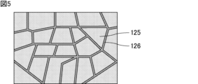
- Figure 5 is a plan view that shows a schematic of the surface of an external electrode formed by electrolytic plating at a high film formation rate.
- convex portions 126 are generated on the surface of the external electrode in a shape that borders random shapes that depend on the grain size of the large crystals 125 in the Al layer 122.
- An automatic appearance inspection machine will erroneously detect this pattern of convex portions 126 as a defective appearance.
- the Cu plating layer 124a does not have any surface irregularities, unlike the Ni plating layer 124b, regardless of the deposition rate.
- Patent Document 2 describes an issue in which the growth rate of the Ni plating formed on the Al electrode differs depending on the crystal plane of the Al electrode, so if the crystals of the Al electrode are large, the Ni does not grow uniformly and unevenness occurs. For this reason, a layer (Al oxide layer) that breaks the continuity of the Al crystals is formed on the surface of the Al metal layer, and a second Al metal layer is formed on that surface to make the Al crystals smaller.
- Patent Document 2 since electroless plating is used, there is no growth from grain boundaries, but the plating similarly grows continuously by taking over the crystals of the Al layer, and by reducing the crystal grain size of the Al layer, unevenness in the plating film is suppressed. As a specific measure, an Al oxide layer is formed on the surface of the Al layer, which increases the electrical resistance of the electrode. Therefore, although the semiconductor device functions as a heat sink, it does not function as an electrode and cannot be used as a capacitor.
- the present invention has been made to solve the above problems, and aims to provide a semiconductor device in which the plating surface of the external electrodes is flat and can be inspected for visual defects using a visual inspection device, as well as a matching circuit and a filter circuit that include the semiconductor device.
- the semiconductor device of the present invention comprises a substrate, an insulating layer provided on the substrate, a first electrode layer provided on the insulating layer, a dielectric film provided on the first electrode layer, a second electrode layer provided on the dielectric film, a moisture-resistant film covering the first electrode layer and the second electrode layer, and an external electrode penetrating the moisture-resistant film, the first electrode layer and the second electrode layer being made of Al or an alloy of Al, the external electrode having a first external electrode and a second external electrode electrically connected to the first electrode layer and the second electrode layer, respectively, the external electrode having a seed layer made of Cu/Ti, Cu/Cr or Cu/Nichrome, and a plating layer provided on the seed layer, the horizontal crystal grain size of the seed layer being 500 nm or less, and the horizontal crystal grain size of the plating layer being 500 nm or less.
- the matching circuit of the present invention includes the semiconductor device of the present invention.
- the filter circuit of the present invention includes the semiconductor device of the present invention.
- the present invention provides a semiconductor device in which the plating surface of the external electrodes is flat and can be inspected for visual defects using a visual inspection device, as well as a matching circuit and a filter circuit that include the semiconductor device.
- FIG. 1 is a cross-sectional view showing a schematic diagram of a plating layer formed by electrolytic plating at a slow film formation rate, and shows the initial stage of electrolytic plating.
- FIG. 2 is a cross-sectional view showing a schematic diagram of a plating layer formed by electrolytic plating at a slow film formation rate, and shows the state after the electrolytic plating is completed.
- FIG. 3 is a cross-sectional view showing a schematic diagram of a plating layer formed by electrolytic plating at a high film formation rate, showing the initial stage of electrolytic plating.
- FIG. 4 is a cross-sectional view showing a schematic diagram of a plating layer formed by electrolytic plating at a high film formation rate, showing the state after the electrolytic plating is completed.
- FIG. 1 is a cross-sectional view showing a schematic diagram of a plating layer formed by electrolytic plating at a slow film formation rate, and shows the initial stage of electrolytic plating.
- FIG. 3 is a cross
- FIG. 5 is a plan view showing a schematic view of the surface of an external electrode formed by electrolytic plating at a high film formation rate.
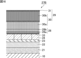
- FIG. 6 is a cross-sectional view illustrating an example of a capacitor according to the first embodiment of the present invention.
- FIG. 7 is a plan view illustrating an example of a capacitor according to the first embodiment of the present invention.
- FIG. 8 is a cross-sectional view of the capacitor shown in FIG. 6, focusing on a region in which a first external electrode is formed.
- FIG. 9 is a cross-sectional view of the capacitor shown in FIG. 6, focusing on a region in which the second external electrode is formed.
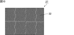
- FIG. 10 is an enlarged plan view showing a schematic view of the surface of an external electrode of the capacitor shown in FIG. FIG.
- FIG. 11 is a cross-sectional view showing a schematic example of a capacitor according to a second embodiment of the present invention, focusing on a first external electrode forming region.
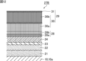
- FIG. 12 is a cross-sectional view showing a schematic example of a capacitor according to a second embodiment of the present invention, focusing on a second external electrode forming region.
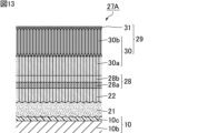
- FIG. 13 is a cross-sectional view showing a schematic example of a capacitor according to a third embodiment of the present invention, focusing on a first external electrode forming region.
- FIG. 14 is a cross-sectional view showing a schematic example of a capacitor according to a third embodiment of the present invention, focusing on a second external electrode forming region.
- FIG. 12 is a cross-sectional view showing a schematic example of a capacitor according to a second embodiment of the present invention, focusing on a first external electrode forming region.
- FIG. 13 is a cross-sectional view showing a schematic example of a capacitor according to a third embodiment of the present
- FIG. 15 is a cross-sectional view showing a schematic example of a capacitor according to a fourth embodiment of the present invention, focusing on a first external electrode forming region.
- FIG. 16 is a cross-sectional view showing a schematic example of a capacitor according to a fourth embodiment of the present invention, focusing on a second external electrode forming region.
- FIG. 17 is a plan view illustrating an example of the dividing layer illustrated in FIGS. 15 and 16.
- FIG. 18 is a plan view diagrammatically illustrating another example of the dividing layer shown in FIGS. 15 and 16.
- FIG. 19 is an explanatory diagram showing an example of a matching circuit including a semiconductor device of the present invention.
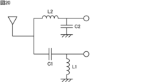
- FIG. 20 is an explanatory diagram showing an example of a filter circuit including the semiconductor device of the present invention.
- the present invention is not limited to the following configurations, and can be appropriately modified and applied within the scope of the present invention. Note that the present invention also includes a combination of two or more of the individual preferred configurations of the present invention described below.
- each embodiment will be referred to simply as the "semiconductor device of the present invention.”
- the shape and arrangement of each component of the semiconductor device of the present invention are not limited to the examples shown in the drawings.
- the semiconductor device of the present invention may be a capacitor itself (i.e., a capacitor element), or may be a device that includes a capacitor.
- the surface roughness Ra of the insulating layer below the first electrode layer is controlled to be 5 nm or more and 500 nm or less.
- FIG. 6 is a cross-sectional view showing an example of a capacitor according to the first embodiment of the present invention.
- FIG. 7 is a plan view showing an example of a capacitor according to the first embodiment of the present invention.
- FIG. 6 is a cross-sectional view taken along line I-I of the capacitor shown in FIG. 7.
- the length direction, width direction, and thickness direction of a capacitor are defined as the directions indicated by arrows L, W, and T, respectively, as shown in Figures 6 and 7.
- the length direction L, width direction W, and thickness direction T are mutually orthogonal.
- the 6 and 7 includes a substrate 10, an insulating layer 21 provided on the substrate 10, a first electrode layer 22 provided on the insulating layer 21, a dielectric film 23 provided on the first electrode layer 22, a second electrode layer 24 provided on the dielectric film 23, a moisture-resistant film 25 covering the first electrode layer 22 and the second electrode layer 24, a protective layer 26 provided on the moisture-resistant film 25, and an external electrode 27 penetrating the moisture-resistant film 25 and the protective layer 26.
- the first electrode layer 22 and the second electrode layer 24 are made of Al or an alloy of Al.
- the external electrode 27 includes a first external electrode 27A connected to the first electrode layer 22 and a second external electrode 27B connected to the second electrode layer 24.
- the first external electrode 27A penetrates the protective layer 26, the moisture-resistant film 25, and the dielectric film 23, and the second external electrode 27B penetrates the protective layer 26 and the moisture-resistant film 25.
- the external electrodes 27 (first external electrode 27A and second external electrode 27B) have a seed layer 28 made of Cu/Ti, Cu/Cr, or Cu/nichrome, and a plating layer 29 provided on the seed layer 28.
- the first electrode layer 22, the dielectric film 23, and the second electrode layer 24 are stacked in this order to form a MIM (Metal Insulator Metal) capacitor structure.
- MIM Metal Insulator Metal
- FIG. 8 is a cross-sectional view of the capacitor shown in FIG. 6, focusing on the first external electrode formation region.
- FIG. 9 is a cross-sectional view of the capacitor shown in FIG. 6, focusing on the second external electrode formation region.
- the horizontal crystal grain size of the seed layer 28 is 500 nm or less
- the horizontal crystal grain size of the plating layer 29 is 500 nm or less.
- the plating surfaces of the first external electrode 27A and the second external electrode 27B flat.
- the surface roughness Ra of the first external electrode 27A and the second external electrode 27B is 500 nm or less.
- a visual inspection device can generally detect defects of 0.5 to 1 ⁇ m or more in size (peeling, dirt, scratches, pattern defects, etc.), it is possible to inspect the capacitor 1, and in particular the external electrode 27, for visual defects using the visual inspection device.
- FIG. 10 is a schematic plan view showing an enlarged view of the surface of the external electrode of the capacitor shown in FIG. 7.
- the appearance inspection device may erroneously detect the unevenness of the plating surface of the external electrode 27 as an appearance defect.
- the horizontal crystal grain size of the seed layer 28 is preferably 5 nm or more and 500 nm or less, and more preferably 5 nm or more and 200 nm or less.
- the horizontal crystal grain size of the plating layer 29 is preferably 5 nm or more and 500 nm or less, and more preferably 5 nm or more and 200 nm or less.
- the horizontal crystal grain size is measured by observing the cross section of the layer with a scanning electron microscope (SEM), measuring the grain size (maximum length) of 50 random crystal grains in the in-plane direction (direction perpendicular to the thickness direction) in the observed image, and calculating the average.
- SEM scanning electron microscope
- the rough surface of the base layer of the first external electrode 27A and the second external electrode 27B made of Al or an Al alloy makes the crystal grain size of the first external electrode 27A and the second external electrode 27B small during film formation, and is also unlikely to become large during subsequent heat treatment. This reduces the horizontal crystal grain size of the seed layer 28 on the first external electrode 27A and the second external electrode 27B, as described above, and the horizontal crystal grain size of the plating layer (preferably a Ni plating layer) on the seed layer 28. As a result, the unevenness of the surfaces of the first external electrode 27A and the second external electrode 27B can be controlled to be small.
- the surface roughness Ra of the insulating layer 21 below the first electrode layer 22 is 5 nm or more and 500 nm or less
- the first electrode layer 22 and the second electrode layer 24 contain crystals grown according to the surface roughness of the insulating layer 21
- the horizontal crystal grain size of the first electrode layer 22 and the second electrode layer 24 is 500 nm or less
- the seed layer 28 contains crystals grown by inheriting the crystals of the first electrode layer 22 and the second electrode layer 24.
- the horizontal crystal grain size of the plating layer preferably a Ni plating layer
- the horizontal crystal grain size of the plating layer that grows by inheriting the crystals of the seed layer 28 can be set to 500 nm or less.
- the horizontal crystal grain size of the first electrode layer 22 above it can be controlled to 500 nm or less.
- the horizontal crystal grain size of the seed layer 28 and plating layer 29 of the first external electrode 27A, which have grown by inheriting the crystals of the first electrode layer 22, can also be controlled to 500 nm or less.
- the horizontal crystal grain size of the first electrode layer 22 thereon can be controlled to 500 nm or less, and further, the surface roughness of the dielectric film 23 above the first electrode layer 22 can also be controlled (preferably 5 nm or more and 500 nm or less).
- the horizontal crystal grain size of the second electrode layer 24 above the dielectric film 23 can be controlled to 500 nm or less. Therefore, the horizontal crystal grain size of the seed layer 28 and plating layer 29 of the second electrode layer 24 that have grown by inheriting the crystals of the second electrode layer 24 can also be 500 nm or less.
- the surface of the insulating layer 21 (e.g., SiO 2 ) under the first electrode layer 22 is not roughened by a normal film formation method such as thermal oxidation of Si, sputtering, CVD (chemical vapor deposition), or deposition, and the surface roughness Ra is less than 5 nm. If the surface roughness Ra of the insulating layer 21 is less than 5 nm, the crystals of the first electrode layer 22 and the second electrode layer 24 are not refined. Therefore, the surface roughness can be adjusted to a desired value by grinding or polishing the surface of the insulating layer 21, or etching the surface by dry etching such as reactive ion etching (RIE) or milling, or wet etching using hydrofluoric acid.
- RIE reactive ion etching
- surface roughness Ra can be measured as the arithmetic mean roughness Ra measured in accordance with JIS-B0601:2001.
- the surface roughness Ra of the insulating layer 21 is preferably 5 nm or more and 500 nm or less, and more preferably 5 nm or more and 200 nm or less.
- the period of the unevenness on the surface of the insulating layer 21 is preferably controlled to be 20 nm or more and 500 nm or less, and more preferably 20 nm or more and 200 nm or less.
- the horizontal crystal grain size of the first electrode layer 22 and the second electrode layer 24 is preferably 5 nm or more and 500 nm or less, and more preferably 5 nm or more and 200 nm or less.
- the substrate 10 is not particularly limited, but is preferably a semiconductor substrate such as a silicon substrate or a gallium arsenide substrate.
- the insulating layer 21 is provided so as to cover the entirety of one of the main surfaces of the substrate 10.
- the insulating layer 21 may be provided so as to cover a portion of one of the main surfaces of the substrate 10, but it must be provided in an area that is larger than the first electrode layer 22 and that overlaps the entirety of the first electrode layer 22.
- the material constituting the insulating layer 21 is not particularly limited, but preferable examples include SiO2 , SiN, Al2O3 , HfO2 , Ta2O5 , ZrO2 , etc. All of these materials are amorphous.
- the first electrode layer 22 is provided at a position away from the edge of the substrate 10. In other words, the edge of the first electrode layer 22 is located inside the edge of the substrate 10.
- the first electrode layer 22 is made of Al or an Al alloy.
- Al alloys include AlSi.
- the dielectric film 23 is provided so as to cover the first electrode layer 22 except for the opening.
- the end of the dielectric film 23 is also provided on the surface of the insulating layer 21 from the end of the first electrode layer 22 to the end of the substrate 10. The end of the dielectric film 23 does not have to be provided to the end of the substrate 10.
- the material constituting the dielectric film 23 is not particularly limited, but preferably includes oxides or nitrides such as SiO2 , SiN , Al2O3 , HfO2 , and Ta2O5 .
- the second electrode layer 24 is disposed opposite the first electrode layer 22 with the dielectric film 23 in between.
- the second electrode layer 24 is made of Al or an Al alloy.
- Al alloys include AlSi.
- the moisture-resistant film 25 is provided so as to cover the dielectric film 23 and the second electrode layer 24 except for the opening. The provision of the moisture-resistant film 25 enhances the moisture resistance of the capacitor element, particularly the dielectric film 23.
- the material constituting the moisture-resistant film 25 is not particularly limited, but preferably includes moisture-resistant materials such as SiO 2 and SiN.
- the protective layer 26 has openings at positions overlapping the openings of the dielectric film 23 and moisture-resistant film 25 (openings overlapping the first electrode layer 22) and at a position overlapping the opening of the moisture-resistant film 25 (openings overlapping the second electrode layer 24).
- the provision of the protective layer 26 protects the capacitor element, and in particular the dielectric film 23, from moisture. Note that the protective layer 26 does not necessarily have to be provided.
- the material constituting the protective layer 26 is not particularly limited, but preferred examples include resin materials such as polyimide resin and solder resist resin.
- the external electrodes 27 (first external electrode 27A and second external electrode 27B) have a multi-layer structure, and from the substrate 10 side, have a seed layer 28 and a plating layer 29.
- the outermost surface of the external electrodes 27 is preferably made of Au or Sn.
- the seed layer 28 is made of Cu/Ti, Cu/Cr, or Cu/Nichrome. Such a seed layer 28 can grow continuously while inheriting the crystallinity of the surface of the first electrode layer 22 or the second electrode layer 24.
- element A/element B refers to a laminate in which a conductive layer made of element B and a conductive layer made of element A are laminated in this order from the substrate side.
- the seed layer 28 may be a laminate in which a Ti layer 28a and a Cu layer 28b are laminated in this order from the substrate 10 side, as shown in Figures 8 and 9.
- the seed layer 28 is formed by sputtering or vapor deposition.
- the seed layer 28 for example a Cu/Ti layer
- the Q value of the capacitor will deteriorate due to the resistance of the natural oxide film on the surface of this Al electrode layer. Therefore, by performing surface dry etching such as milling in a vacuum immediately before forming the seed layer 28 and then continuously forming the seed layer 28 in a vacuum, the influence of the natural oxide film on the surface of the Al electrode layer can be eliminated and the Al electrode layer and the seed layer 28 can be connected with low resistance.
- the seed layer 28 grows by taking over the crystals on the surface of the Al electrode layer, so that the horizontal crystal grain size of the seed layer 28 can be controlled to 500 nm or less.
- the seed layer 28 is formed on an electrode layer made of an Al alloy.
- the plating layer 29 has, in order from the substrate 10 side, a first plating layer 30 and a second plating layer 31.
- the material of the first plating layer 30 is not particularly limited, but it is preferable for it to include a Ni plating layer formed by electrolytic plating of Ni. As described above, if the deposition rate is increased, the surface of the Ni plating layer is likely to have protrusions, but in this embodiment, since the horizontal crystal grain size of the seed layer 28 is 500 nm or less, even if the deposition rate is increased, the crystal grain size of the Ni plating layer is also 500 nm or less, and the unevenness of the surface of the Ni plating layer can be effectively reduced.
- the first plating layer 30 may be a single-layer structure of a Ni plating layer, or may be a laminated structure in which a Cu plating layer 30a and a Ni plating layer 30b are laminated in this order from the substrate 10 side, as shown in Figures 8 and 9.
- Examples of materials that can be used for the second plating layer 31 include gold (Au) and tin (Sn).
- an Au/Ni/Cu layer or an Au/Ni layer may be formed on the seed layer 28 by electrolytic plating.
- the crystal grain size of the underlying electrode layer first electrode layer 22 or second electrode layer 24
- the plating surface of the Cu or Ni layer becomes rough when the deposition rate is increased.
- the crystal grain size of the underlying electrode layer to be small, the plating surface does not become rough even if the deposition rate is maximized below the current density at which the plating solution does not decompose.
- the plating film that grows from the crystal grain boundaries of the seed layer 28 covers the grain boundaries at an early stage by making the crystal grain size of the seed layer 28 sufficiently small, and after the entire surface is covered, the entire surface grows at the same deposition rate. Similarly, the second and subsequent plating layers do not become rough.
- the constituent materials of the first external electrode 27A and the second external electrode 27B may be the same or different.
- the capacitor 1 shown in Figures 6 and 7 is manufactured, for example, by the method described in Patent Document 3.
- the capacitor according to the second embodiment of the present invention differs from the first embodiment in that the surface roughness Ra of the Si single crystal substrate is controlled to be 5 nm or more and 500 nm or less.
- the film thickness of the insulating layer 21 becomes non-uniform, which may cause the parasitic capacitance via the semiconductor substrate to become non-uniform, resulting in a deterioration in the capacitance accuracy of the capacitor 1.
- FIG. 11 is a cross-sectional view showing a schematic example of a capacitor according to a second embodiment of the present invention, focusing on the first external electrode formation region.
- FIG. 12 is a cross-sectional view showing a schematic example of a capacitor according to a second embodiment of the present invention, focusing on the second external electrode formation region.
- the substrate 10 is a Si single crystal substrate 10a
- the surface roughness Ra of the Si single crystal substrate 10a is 5 nm or more and 500 nm or less
- the insulating layer 21 is formed along the surface of the Si single crystal substrate 10a.
- the roughening of the Si single crystal substrate 10a can be adjusted to the desired surface roughness by grinding or polishing the flat surface of the Si single crystal substrate, or by etching using dry etching such as reactive ion etching (RIE) or milling, or wet etching using an organic alkaline solution.
- RIE reactive ion etching
- the insulating layer 21 on top of it can also have a similar surface roughness.
- the surface roughness Ra of the Si single crystal substrate 10a is preferably 5 nm or more and 500 nm or less, and more preferably 5 nm or more and 200 nm or less.
- the period of the unevenness on the surface of the Si single crystal substrate 10a is preferably controlled to 20 nm or more and 500 nm or less, and more preferably 20 nm or more and 200 nm or less.
- the capacitor according to the third embodiment of the present invention differs from the first embodiment in that a polycrystalline Si layer having a surface roughness Ra controlled to 5 nm or more and 500 nm or less is formed on a single crystal Si substrate having a flat surface.
- FIG. 13 is a cross-sectional view showing a schematic example of a capacitor according to a third embodiment of the present invention, focusing on the first external electrode formation region.
- FIG. 14 is a cross-sectional view showing a schematic example of a capacitor according to a third embodiment of the present invention, focusing on the second external electrode formation region.
- the substrate 10 has a flat surface of a single crystal Si substrate 10b and a polycrystalline Si layer 10c formed on the surface of the single crystal Si substrate 10b, and the surface roughness Ra of the polycrystalline Si layer 10c is 5 nm or more and 500 nm or less.
- the polycrystalline Si layer 10c with a controlled surface roughness Ra below the insulating layer 21 and forming the insulating layer 21 along the surface of the polycrystalline Si layer 10c, it is possible to roughen the surface of the insulating layer 21 without degrading the film thickness accuracy of the insulating layer 21. Therefore, the capacitance variation of the capacitor due to the film thickness distribution of the insulating layer 21 can be reduced.
- the grain size of the polycrystals can be controlled with precision. Therefore, the surface roughness Ra of the substrate 10 can be controlled more precisely (more uniformly and more constant) than when other methods such as etching or grinding are used as in the second embodiment.
- the polycrystalline Si layer 10c is formed by depositing a polycrystalline Si film on the surface of a flat single crystal Si substrate 10b by a CVD method or the like.
- the crystal grain size of the polycrystalline Si layer 10c can be easily controlled to a stable size compared to the amorphous insulating layer 21 and the single crystal Si substrate 10b.
- the surface roughness of the insulating layer 21 formed thereon can be more easily controlled to the desired roughness.
- the surface roughness Ra of the polycrystalline Si layer 10c By controlling the surface roughness Ra of the polycrystalline Si layer 10c to be 5 nm or more and 500 nm or less, the insulating layer 21 on top can also have an equivalent surface roughness.
- the surface roughness Ra of the polycrystalline Si layer 10c is preferably 5 nm or more and 500 nm or less, and more preferably 5 nm or more and 200 nm or less.
- the period of the unevenness on the surface of the polycrystalline Si layer 10c is preferably controlled to be 20 nm or more and 500 nm or less, and more preferably 20 nm or more and 200 nm or less.
- the surface roughness Ra of the Si single crystal substrate 10b is not particularly limited, but the Si single crystal substrate 10b is usually mirror-finished and has a surface roughness Ra of less than 5 nm.
- the capacitor according to the fourth embodiment of the present invention differs from the first embodiment in that the surfaces of the first and second electrode layers further include a dividing layer formed of a material that prevents the seed layer thereon from inheriting the crystallinity of the first and second electrode layers.
- the surfaces of the first and second electrode layers usually have a natural oxide film of Al or an Al alloy, and forming a seed layer (e.g., a Cu/Ti layer) on top of it in this state results in a large resistance and deteriorates the Q value of the capacitor.
- a seed layer e.g., a Cu/Ti layer
- FIG. 15 is a cross-sectional view showing a schematic example of a capacitor according to a fourth embodiment of the present invention, focusing on the first external electrode formation region.
- FIG. 16 is a cross-sectional view showing a schematic example of a capacitor according to a fourth embodiment of the present invention, focusing on the second external electrode formation region.
- the surfaces of the first electrode layer 22 and the second electrode layer 24 are further provided with dividing layers 33 formed of a material that does not inherit the crystallinity of the first electrode layer 22 and the second electrode layer 24, in a pattern with a period of 500 nm or less, and the seed layer 28 thereon is made of a material that does not inherit the crystallinity of the first electrode layer 22 and the second electrode layer 24.
- This makes it possible to make the horizontal crystal grain size of the seed layer 28 500 nm or less. Therefore, it becomes possible to inspect the capacitor 1, and in particular the external electrode 27, for visual defects using a visual inspection device.
- the Cu/Ti layer grows as uniaxially oriented crystals with Ti at (0001) and Cu at (111) in the direction perpendicular to the oxide film of the Al electrode layer, and in the area where the oxide film has been removed, grows as crystals that inherit the random crystal orientation of the Al film.
- the horizontal crystal grain size of the seed layer 28 can be made 500 nm or less.
- the formation of the dividing layer 33 i.e., the patterning of the oxide film of the first electrode layer 22 and the second electrode layer 24, can be performed, for example, as follows. First, a metal oxide film (e.g., an Al oxide film) is additionally formed on the surface of the natural oxide film (e.g., an Al oxide film) of the first electrode layer 22 and the second electrode layer 24, and then the metal oxide film is patterned by photolithography and a dry etching method or a wet etching method. Then, just before depositing the seed layer 28 by sputtering, the natural oxide film that has been generated again is removed by a dry etching method by an amount corresponding to the thickness of the film, and the seed layer 28 is deposited.
- a metal oxide film e.g., an Al oxide film
- the natural oxide film that has been generated again is removed by a dry etching method by an amount corresponding to the thickness of the film, and the seed layer 28 is deposited.
- Materials that can be formed on the surface of the natural oxide film (e.g., Al oxide film) on the surfaces of the first electrode layer 22 and the second electrode layer 24 may be Si, Ta, SiO 2 , SiN, etc., in addition to Al oxide film. This makes it possible to reduce the electrical resistance between the first electrode layer 22 and the second electrode layer 24 and the seed layer 28, and similarly makes it possible to make the horizontal crystal grain size of the plating layer 29 formed thereon 500 nm or less, thereby reducing the surface unevenness.
- the period of the pattern of the dividing layer 33 is preferably greater than 0 nm and less than 500 nm, and more preferably greater than 20 nm and less than 200 nm.
- FIG. 17 is a plan view showing a schematic example of the dividing layer shown in FIGS. 15 and 16.
- FIG. 18 is a plan view showing a schematic example of another dividing layer shown in FIGS. 15 and 16.
- the dividing layer 33 is preferably formed in a pattern in which dots 34, such as squares such as rectangles or circles, are periodically arranged in a two-dimensional manner.
- each dot 34 is made of a material that does not inherit the crystals of the first electrode layer 22 and the second electrode layer 24, and the pitch between adjacent dots 34 is 500 nm or less.
- the size of each dot 34 is preferably approximately the same as the desired crystal grain size in the horizontal direction of the seed layer 28 and the plating layer 29.
- the exposed area of the first electrode layer 22 and the second electrode layer 24 (the area of the region not covered by the dividing layer 33 (dots 34)) is preferably 50% or more, and more preferably 70% or more.
- Figures 17 and 18 show a case where all dots 34 have the same planar shape
- the pattern of the dividing layer 33 may be a pattern in which dots of different planar shapes are mixed.
- the horizontal crystal grain size of the underlying seed layer is 500 nm or less, it is possible to almost completely improve the detection of surface irregularities on the external electrode caused by crystal grain boundaries as defects. This is thought to be because the horizontal crystal grain size of the Ni plating layer is also 500 nm or less, just like the seed layer. It was also found that if the horizontal crystal grain size of the underlying seed layer is 200 nm or less, surface irregularities on the external electrode caused by crystal grain boundaries are not detected as defects. This is thought to be because the horizontal crystal grain size of the Ni plating layer is also 200 nm or less, just like the seed layer.
- the semiconductor device of the present invention is preferably used as a capacitor in a matching circuit or a filter circuit.
- a matching circuit or a filter circuit including the semiconductor device of the present invention is also one aspect of the present invention.
- FIG. 19 is an explanatory diagram showing an example of a matching circuit equipped with the semiconductor device of the present invention.
- the semiconductor device of the present invention can be used for the capacitor C of the matching circuit shown in FIG. 19.
- FIG. 20 is an explanatory diagram showing an example of a filter circuit equipped with a semiconductor device of the present invention.
- the semiconductor device of the present invention can be used for the capacitor C1 of the filter circuit shown in FIG. 20.
- the external electrodes each have a seed layer made of Cu/Ti, Cu/Cr, or Cu/nichrome, and a plating layer provided on the seed layer, the seed layer has a horizontal crystal grain size of 500 nm or less;
- the semiconductor device wherein the horizontal crystal grain size of the plating layer is 500 nm or less.
- the surface roughness Ra of the insulating layer is 5 nm or more and 500 nm or less
- the first electrode layer and the second electrode layer include crystals grown according to the surface roughness of the insulating layer
- the first electrode layer and the second electrode layer have a horizontal crystal grain size of 500 nm or less
- the substrate is a Si single crystal substrate,
- the surface roughness Ra of the Si single crystal substrate is 5 nm or more and 500 nm or less,
- the substrate has a single crystal Si substrate having a flat surface and a polycrystalline Si layer formed on the surface of the single crystal Si substrate;
- the semiconductor device described in ⁇ 1> further comprises a dividing layer formed on the surfaces of the first electrode layer and the second electrode layer in a pattern with a period of 500 nm or less, and the seed layer thereon is made of a material that does not inherit the crystallinity of the first electrode layer and the second electrode layer.
- a matching circuit comprising the semiconductor device according to any one of ⁇ 1> to ⁇ 5>.
- a filter circuit comprising the semiconductor device according to any one of ⁇ 1> to ⁇ 5>.
- Capacitor semiconductor device
- REFERENCE SIGNS LIST 10
- Polycrystalline Si layer 21 Insulating layer 22
- First electrode layer 23 Dielectric film 24
- Second electrode layer 25
- Moisture-resistant film 26
- Protective layer 27
- External electrode 27A
- First external electrode 27B
- Second external electrode 28
- Seed layer 28a
- Ti layer 28b
- Cu layer 29
- Second plating layer 34
Landscapes
- Engineering & Computer Science (AREA)
- Power Engineering (AREA)
- Microelectronics & Electronic Packaging (AREA)
- Manufacturing & Machinery (AREA)
- Semiconductor Integrated Circuits (AREA)
Abstract
基板10と、基板10上に設けられた絶縁層21と、絶縁層21上に設けられた第1電極層22と、第1電極層22上に設けられた誘電体膜23と、誘電体膜23上に設けられた第2電極層24と、第1電極層22及び第2電極層24を覆う耐湿膜25と、耐湿膜25を貫通する外部電極27と、を備え、第1電極層22及び第2電極層24は、Al又はAlの合金からなり、外部電極27は、第1電極層22及び第2電極層24とそれぞれ電気的に接続された第1外部電極27A及び第2外部電極27Bを有し、外部電極27は、Cu/Ti、Cu/Cr又はCu/ニクロムからなるシード層28と、シード層28上に設けられためっき層29と、を有し、シード層28の水平方向の結晶粒径が500nm以下であり、めっき層29の水平方向の結晶粒径が500nm以下である、半導体装置1。
Description
本発明は、半導体装置、マッチング回路及びフィルタ回路に関する。
特許文献1の図1及び図2には、基板上に絶縁層、第1電極層、誘電体層、第2電極層、耐湿保護層及び樹脂保護層が順次形成された半導体装置が記載されている。耐湿保護層、樹脂保護層等を貫通して第1及び第2電極層の一部表面を露出したビアを形成し、その上にシード層、第1めっき層及び第2めっき層からなる第1及び第2外部電極を形成している。
特許文献2には、Al電極の表面上に、無電解めっき法により、均一な膜厚のNi層を形成する技術が記載されている。
特許文献3には、基板と、上記基板上に設けられた第1電極層と、上記第1電極層上に設けられた誘電体膜と、上記誘電体膜上に設けられた第2電極層と、上記第1電極層及び上記第2電極層を覆う保護層と、上記保護層を貫通する外部電極と、を備え、上記誘電体膜はシリコン窒化物からなり、上記誘電体膜に含有されるSiとNの総量に対するSiの原子濃度比が43atom%以上70atom%以下である、半導体装置が開示されている。
特許文献1では、半導体プロセスを用いており、電極層にはAlが用いられる。
図1は、遅い成膜レートで電解めっきによりめっき層を形成した場合を模式的に示す断面図であり、電解めっきの初期段階の状態を示す。図2は、遅い成膜レートで電解めっきによりめっき層を形成した場合を模式的に示す断面図であり、電解めっきの完了後の状態を示す。
図1に示すように、Al層122は、下地121がSiO2、SiN等のアモルファス膜の場合、Alの成膜温度や、その上の誘電体層(SiN膜)、樹脂保護層(ポリイミド)の熱処理により再結晶化が進む。そして、結晶の向きがランダムな多結晶膜となり、結晶の大きさが、膜厚方向0.1~2μm程度に対して、水平方向には数~10μm程度の大きさにまで成長する。
なお、図1等の断面図において、各層の縦線は結晶粒界を示す。
また、図1に示すように、このAl層122上に形成される外部電極のシード層123は、通常、スパッタ法により形成されたTi層123a及びCu層123bから構成されるが、Ti層123a及びCu層123bは、Al層122の表面の結晶性を引継いで連続的に膜成長する。そのため、Ti層123a及びCu層123bの水平方向の結晶粒径は、Al層122と同じ数~10μmとなる。
更に、シード層123の上に形成するめっき層124は、Cu、Ni、Au等で電解めっきにより形成するが、その際、Niめっきの膜成長は、成膜レートが充分遅い場合は、シード層123の粒界部から優先的に成長し、粒界部以外の表面からの成長は非常に遅い(図1参照)。そのため、図2に示すように、粒界部からの膜成長が水平方向に進み、全面が覆われる間に、膜厚方向への成長が進まず、全面が覆われた後は、全面で成膜レートは一定のため、Niめっき層124bの表面の凹凸が小さくなる。しかしながら、成膜レートを遅くすると、コストが増大してしまう。
図3は、早い成膜レートで電解めっきによりめっき層を形成した場合を模式的に示す断面図であり、電解めっきの初期段階の状態を示す。図4は、早い成膜レートで電解めっきによりめっき層を形成した場合を模式的に示す断面図であり、電解めっきの完了後の状態を示す。
それに対して、成膜レートを早くすると、図3に示すように、Niめっきにおいて、粒界部とそれ以外の表面の成長速度の差が縮まり、図4に示すように、粒界部からの膜成長で全面が覆われず、成長の早い粒界上においてNiめっき層124bの表面が突起となる。
この突起により、外部電極の外観が著しくランダムに粗い状態となり、外部電極上のその他の外観不良(膜剥がれ、ごみ、傷、パターン不良等)を自動外観検査機で検査できなくなってしまう。自動外観検査機で検査するためには、めっきの表面粗さRaは、500nm以下となっている必要がある。
図5は、早い成膜レートで電解めっきにより形成した外部電極の表面を模式的に示す平面図である。
Al層122の水平方向の結晶粒径が数~10μmであると、図5に示すように、外部電極の表面には、Al層122の大きな結晶125の粒径に依存したランダムな形状を縁取りしたような形状で凸部126が生成する。そして、この凸部126のパターンを自動外観検査機が外観不良として誤検出してしまう。
なお、Cuめっき層124aに関しては、図1~図4に示したように、成膜レートに関わらず、Niめっき層124bのような凹凸は表面に発生しない。
特許文献3に記載のキャパシタとして機能し得る半導体装置についても、外部電極をNiめっきで形成した場合、同様の課題が発生し得る。
特許文献2には、Al電極上に形成するNiめっきの成長速度が、Al電極の結晶面によって異なるため、Al電極の結晶が大きいとNiが均一に成長せず、凹凸ができてしまうことが課題として記載されている。そのため、Al金属層の表面にAl結晶の連続性を断ち切る層(Al酸化物層)を形成して、その表面に第2のAl金属層を形成してAlの結晶を小さくしている。それにより、Ni層が成長し難い結晶粒の表面上に直接Ni層が成長しなくても、その結晶粒の周囲で形成されたNi層が、Al電極表面に平行な方向(横方向)に成長することで、Ni層が成長し難い結晶粒の表面がNi層で覆われ、均一なNi層を形成している(特許文献2の図1参照)。
特許文献2では、無電解めっきのため、粒界からの成長はないが、Al層の結晶を引継いで連続的にめっきが成長することは同様であり、Al層の結晶粒径を小さくすることで、めっき膜の凹凸を抑制している。具体的な対策として、Al層の表面にAl酸化物層を形成しおり、電極の電気抵抗が高くなる。したがって、当該半導体装置は、ヒートシンクとしては機能するが、電極としては機能しないため、キャパシタには適用できない。
本発明は、上記の問題を解決するためになされたものであり、外部電極のめっき表面が平坦になり、外観検査装置で外観不良を検査可能な半導体装置、並びに、上記半導体装置を備えるマッチング回路及びフィルタ回路を提供することを目的とする。
本発明の半導体装置は、基板と、上記基板上に設けられた絶縁層と、上記絶縁層上に設けられた第1電極層と、上記第1電極層上に設けられた誘電体膜と、上記誘電体膜上に設けられた第2電極層と、上記第1電極層及び上記第2電極層を覆う耐湿膜と、上記耐湿膜を貫通する外部電極と、を備え、上記第1電極層及び上記第2電極層は、Al又はAlの合金からなり、上記外部電極は、上記第1電極層及び上記第2電極層とそれぞれ電気的に接続された第1外部電極及び第2外部電極を有し、上記外部電極は、Cu/Ti、Cu/Cr又はCu/ニクロムからなるシード層と、上記シード層上に設けられためっき層と、を有し、上記シード層の水平方向の結晶粒径が500nm以下であり、上記めっき層の水平方向の結晶粒径が500nm以下である。
本発明のマッチング回路は、本発明の半導体装置を備える。
本発明のフィルタ回路は、本発明の半導体装置を備える。
本発明によれば、外部電極のめっき表面が平坦になり、外観検査装置で外観不良を検査可能な半導体装置、並びに、上記半導体装置を備えるマッチング回路及びフィルタ回路を提供することができる。
以下、本発明の半導体装置、マッチング回路及びフィルタ回路について説明する。
しかしながら、本発明は、以下の構成に限定されるものではなく、本発明の要旨を変更しない範囲において適宜変更して適用することができる。なお、以下において記載する本発明の個々の好ましい構成を2つ以上組み合わせたものもまた本発明である。
しかしながら、本発明は、以下の構成に限定されるものではなく、本発明の要旨を変更しない範囲において適宜変更して適用することができる。なお、以下において記載する本発明の個々の好ましい構成を2つ以上組み合わせたものもまた本発明である。
以下に示す各実施形態は例示であり、異なる実施形態で示した構成の部分的な置換又は組み合わせが可能であることは言うまでもない。第2実施形態以降では、第1実施形態と共通の事項についても記述は省略し、異なる点についてのみ説明する。特に、同様の構成による同様の作用効果については、実施形態毎に逐次言及しない。
以下の説明において、各実施形態を特に区別しない場合、単に「本発明の半導体装置」と言う。本発明の半導体装置及び各構成要素の形状及び配置等は、図示する例に限定されるものではない。
また、以下においては、本発明の半導体装置の一実施形態として、キャパシタを例にとって説明する。本発明の半導体装置は、キャパシタそのもの(すなわちキャパシタ素子)であってもよく、キャパシタを含む装置であってもよい。
[第1実施形態]
本発明の第1実施形態に係るキャパシタでは、第1電極層の下の絶縁層の表面粗さRaを5nm以上、500nm以下に制御する。
本発明の第1実施形態に係るキャパシタでは、第1電極層の下の絶縁層の表面粗さRaを5nm以上、500nm以下に制御する。
図6は、本発明の第1実施形態に係るキャパシタの一例を模式的に示す断面図である。図7は、本発明の第1実施形態に係るキャパシタの一例を模式的に示す平面図である。図6は、図7に示すキャパシタのI-I線に沿った断面図である。
本明細書中、キャパシタ(半導体装置)の長さ方向、幅方向、及び、厚み方向を、図6及び図7等に示すように、各々、矢印L、矢印W、及び、矢印Tで定められる方向とする。ここで、長さ方向Lと幅方向Wと厚み方向Tとは、互いに直交している。
図6及び図7に示すキャパシタ1は、基板10と、基板10上に設けられた絶縁層21と、絶縁層21上に設けられた第1電極層22と、第1電極層22上に設けられた誘電体膜23と、誘電体膜23上に設けられた第2電極層24と、第1電極層22及び第2電極層24を覆う耐湿膜25と、耐湿膜25上に設けられた保護層26と、耐湿膜25及び保護層26を貫通する外部電極27と、を備える。第1電極層22及び第2電極層24は、Al又はAlの合金からなる。外部電極27は、第1電極層22に接続された第1外部電極27Aと、第2電極層24に接続された第2外部電極27Bと、を含む。第1外部電極27Aは保護層26、耐湿膜25及び誘電体膜23を貫通し、第2外部電極27Bは保護層26及び耐湿膜25を貫通する。外部電極27(第1外部電極27A及び第2外部電極27B)は、Cu/Ti、Cu/Cr又はCu/ニクロムからなるシード層28と、シード層28上に設けられためっき層29と、を有する。
キャパシタ1において、第1電極層22と誘電体膜23と第2電極層24とは、この順に積層されており、MIM(Metal Insulator Metal)キャパシタ構造を構成している。第1電極層22と第2電極層24の間に電圧を印加することにより、誘電体膜23に電荷を蓄積することができる。
図8は、図6に示すキャパシタの第1外部電極形成領域に着目した断面図である。図9は、図6に示すキャパシタの第2外部電極形成領域に着目した断面図である。
そして、図8及び図9に示すように、シード層28の水平方向の結晶粒径が500nm以下であり、めっき層29の水平方向の結晶粒径が500nm以下である。このため、第1外部電極27A及び第2外部電極27Bのめっき表面が平坦になる。具体的には、第1外部電極27A及び第2外部電極27Bの表面粗さRaが500nm以下となる。ここで、外観検査装置は、一般的に0.5~1μm以上のサイズの不良(膜剥がれ、ごみ、傷、パターン不良等)を検出可能であることから、キャパシタ1、特に外部電極27の外観不良を外観検査装置で検査することが可能となる。
図10は、図7に示すキャパシタの外部電極の表面を拡大して模式的に示す平面図である。
シード層28及びめっき層29の水平方向の結晶粒径が500nm以下であると、図10に示すように、外部電極27の表面には、シード層28及びめっき層29の小さな結晶32の粒径と同等のサイズの凹凸形状が均一に生成する。このような微細な凹凸パターンは、外観検査装置で検出できないないことから、外部電極27の表面の凹凸を外観不良と誤検出するのを防止することができる。
他方、シード層28の水平方向の結晶粒径が500nmを超え、かつ、めっき層29の水平方向の結晶粒径が500nmを超えると、外観検査装置が外部電極27のめっき表面の凹凸を外観不良として誤検出する場合がある。
シード層28の水平方向の結晶粒径は、5nm以上、500nm以下であることが好ましく、5nm以上、200nm以下であることがより好ましい。めっき層29の水平方向の結晶粒径は、5nm以上、500nm以下であることが好ましく、5nm以上、200nm以下であることがより好ましい。
水平方向の結晶粒径は、当該層の断面を走査電子顕微鏡(SEM)観察し、当該観察画像において任意の50個の結晶粒子の面内方向(厚さ方向に直交する方向)における粒径(最大長)を測定し、その平均を算出することによって測定される。
Al又はAlの合金からなる第1外部電極27A及び第2外部電極27Bの下地層の表面が粗いことで、第1外部電極27A及び第2外部電極27Bの結晶粒径が成膜時に小さくなり、更にその後の熱処理でも大きくなり難い。これにより、上記のように、第1外部電極27A及び第2外部電極27Bの上のシード層28の水平方向の結晶粒径と、シード層28の上のめっき層(好適にはNiめっき層)の水平方向の結晶粒径とが小さくなる。その結果、第1外部電極27A及び第2外部電極27Bの表面の凹凸を小さく制御できる。
より具体的には、本実施形態では、第1電極層22の下の絶縁層21の表面粗さRaが5nm以上、500nm以下であり、第1電極層22及び第2電極層24は、絶縁層21の表面の粗さに従って成長した結晶を含み、第1電極層22及び第2電極層24の水平方向の結晶粒径は、500nm以下であり、シード層28は、第1電極層22及び第2電極層24の結晶を引継いで成長した結晶を含む。その結果、シード層28の結晶を引継いで成長するめっき層(好適にはNiめっき層)の水平方向の結晶粒径を500nm以下とすることができる。
すなわち、第1外部電極27A側では、第1電極層22の下の絶縁層21の表面粗さRaを5nm以上、500nm以下に制御することで、その上の第1電極層22の水平方向の結晶粒径を500nm以下に制御できる。その結果、第1電極層22の結晶を引継いで成長した第1外部電極27Aのシード層28及びめっき層29の水平方向の結晶粒径も500nm以下とすることができる。
また、第2外部電極27B側では、第1電極層22の下の絶縁層21の表面粗さRaを5nm以上、500nm以下に制御することで、その上の第1電極層22の水平方向の結晶粒径を500nm以下に制御でき、更に、第1電極層22の上の誘電体膜23の表面粗さも制御できる(好ましくは5nm以上、500nm以下に制御できる)。その結果、誘電体膜23の上の第2電極層24の水平方向の結晶粒径を500nm以下に制御できる。そのため、第2電極層24の結晶を引継いで成長した第2電極層24のシード層28及びめっき層29の水平方向の結晶粒径も500nm以下とすることができる。
第1電極層22の下の絶縁層21(例えばSiO2)の表面は、Siの熱酸化処理、スパッタ、CVD(化学気相成長)法、蒸着法等の通常の成膜方法では表面粗さRaが5nm未満となり粗化しない。絶縁層21の表面粗さRaが5nm未満の場合、第1電極層22及び第2電極層24の結晶が微細化しない。そのため、絶縁層21の表面を研削や研磨、又は、反応性イオンエッチング(RIE)やミリング法によるドライエッチング法若しくはフッ化水素酸によるウェットエッチング法によりエッチングすることで、所望の表面粗さに調整できる。
本明細書中、表面粗さRaは、JIS-B0601:2001に準拠して測定される算術平均粗さRaとして測定することができる。
絶縁層21の表面粗さRaは、5nm以上、500nm以下であることが好ましく、5nm以上、200nm以下であることがより好ましい。
絶縁層21の表面の凹凸の周期は、20nm以上、500nm以下に制御することが好ましく、20nm以上、200nm以下に制御することがより好ましい。
第1電極層22及び第2電極層24の水平方向の結晶粒径は、5nm以上、500nm以下であることが好ましく、5nm以上、200nm以下であることがより好ましい。
以下、各構成について詳述する。
基板10は、特に限定されないが、好ましくは、シリコン基板又はガリウム砒素基板等の半導体基板である。
絶縁層21は、基板10の一方主面の全体を覆うように設けられている。絶縁層21は、基板10の一方主面の一部を覆うように設けられていてもよいが、第1電極層22よりも大きく、かつ、第1電極層22の全域に重なる領域に設けられる必要がある。
絶縁層21を構成する材料は、特に限定されないが、好ましくは、SiO2、SiN、Al2O3、HfO2、Ta2O5、ZrO2等が挙げられる。いずれの材料もアモルファスである。
第1電極層22は、基板10の端部と離れた位置に設けられている。すなわち、第1電極層22の端部は、基板10の端部よりも内側に位置している。
第1電極層22はAl又はAlの合金からなる。Alの合金としては、例えば、AlSi等が挙げられる。
誘電体膜23は、開口を除く部分で第1電極層22を覆うように設けられている。図6では、誘電体膜23の端部は、第1電極層22の端部から基板10の端部までの絶縁層21の表面上にも設けられている。誘電体膜23の端部は、基板10の端部まで設けられていなくてもよい。
誘電体膜23を構成する材料は、特に限定されないが、好ましくは、SiO2、SiN、Al2O3、HfO2、Ta2O5等の酸化物又は窒化物が挙げられる。
第2電極層24は、誘電体膜23を挟んで第1電極層22に対向して設けられている。
第2電極層24はAl又はAlの合金からなる。Alの合金としては、例えば、AlSi等が挙げられる。
耐湿膜25は、開口を除く部分で誘電体膜23及び第2電極層24を覆うように設けられている。耐湿膜25が設けられていることにより、キャパシタ素子、特に、誘電体膜23の耐湿性が高まる。
耐湿膜25を構成する材料は、特に限定されないが、好ましくは、SiO2、SiN等の耐湿性材料が挙げられる。
保護層26には、誘電体膜23及び耐湿膜25の開口(第1電極層22に重なる開口)に重なる位置と、耐湿膜25の開口(第2電極層24に重なる開口)に重なる位置との各々に開口が設けられている。保護層26が設けられていることにより、キャパシタ素子、特に、誘電体膜23が水分から保護される。なお、保護層26は設けられていなくてもよい。
保護層26を構成する材料は、特に限定されないが、好ましくは、ポリイミド樹脂、ソルダーレジスト樹脂等の樹脂材料が挙げられる。
外部電極27(第1外部電極27A及び第2外部電極27B)は、多層構造であり、基板10側から順に、シード層28と、めっき層29と、を有している。外部電極27の最表面は、Au又はSnから構成されることが好ましい。
シード層28は、Cu/Ti、Cu/Cr又はCu/ニクロムからなる。このようなシード層28は、第1電極層22又は第2電極層24の表面の結晶性を引継いで連続的に膜成長することができる。
なお、本明細書中、元素A/元素Bとは、元素Bからなる導電体層と元素Aからなる導電体層とが基板側からこの順に積層された積層体を意味する。
シード層28は、図8及び図9に示すように、基板10側から順に、Ti層28a及びCu層28bがこの順に積層された積層体であってもよい。
シード層28の成膜方法は、スパッタ又は蒸着法による。しかしながら、Alからなる電極層(第1電極層22又は第2電極層24)の表面に、シード層28、例えばCu/Ti層をそのまま成膜すると、このAl電極層の表面の自然酸化膜による抵抗によってキャパシタのQ値が劣化する。そのため、シード層28の成膜直前に真空中でミリング等の表面ドライエッチングを実施した後、真空中で連続してシード層28を成膜することでAl電極層の表面の自然酸化膜の影響を排除し、Al電極層とシード層28とを抵抗が低い状態で接続することができる。同時に、シード層28はAl電極層の表面の結晶を引継ぎ成長するため、シード層28の水平方向の結晶粒径は500nm以下に制御できる。Alの合金からなる電極層上にシード層28を成膜する場合も同様である。
めっき層29は、基板10側から順に、第1めっき層30及び第2めっき層31を有する。
第1めっき層30の構成材料は、特に限定されないが、Niを電解めっきすることで形成されたNiめっき層を含む場合が好適である。上記のように、成膜レートを早くすると、Niめっき層の表面は突起となり易いが、本実施形態では、シード層28の水平方向の結晶粒径が500nm以下であるため、成膜レートを早くしてもNiめっき層の結晶粒径も500nm以下とし、Niめっき層の表面の凹凸を効果的に小さくすることができる。
第1めっき層30は、Niめっき層の単層構造であってもよいし、図8及び図9に示すように、基板10側から順に、Cuめっき層30a及びNiめっき層30bがこの順に積層された積層構造であってもよい。
第2めっき層31の構成材料としては、例えば、金(Au)、スズ(Sn)等が挙げられる。
より具体的には、電解めっきでシード層28上にAu/Ni/Cu層、又は、Au/Ni層を成膜してもよい。この場合、めっきの1層目となるCu又はNi層は、下地のAl又はAlの合金からなる電極層(第1電極層22又は第2電極層24)の結晶粒径が大きいとき、成膜レートを上げるとめっき表面が粗化する。しかしながら、下地の電極層の結晶粒径を小さく制御することで、成膜レートをめっき液が分解しない電流密度以下で最大にしても、めっきの表面が粗化することはない。これは、シード層28の結晶粒径を充分小さくすることで、シード層28の結晶粒界上から成長しためっき膜が早い段階で粒界間を覆い、全面が覆われた後は全面が同じ成膜レートで成長するためである。めっきの2層目以降も同様に粗化しない。
第1外部電極27Aの構成材料と第2外部電極27Bの構成材料とは、互いに同じであってもよいし、互いに異なっていてもよい。
図6及び図7に示すキャパシタ1は、例えば、特許文献3に記載された方法で製造される。
[第2実施形態]
本発明の第2実施形態に係るキャパシタでは、Si単結晶基板の表面粗さRaを5nm以上、500nm以下に制御する点で、第1実施形態と異なる。
本発明の第2実施形態に係るキャパシタでは、Si単結晶基板の表面粗さRaを5nm以上、500nm以下に制御する点で、第1実施形態と異なる。
第1実施形態では、絶縁層21の表面粗さをエッチング等で調整する場合、絶縁層21の膜厚が不均一になるため、半導体基板を介した寄生容量が不均一となり、キャパシタ1の容量精度が劣化するおそれがある。
図11は、本発明の第2実施形態に係るキャパシタの一例を模式的に示す断面図であり、第1外部電極形成領域に着目した図である。図12は、本発明の第2実施形態に係るキャパシタの一例を模式的に示す断面図であり、第2外部電極形成領域に着目した図である。
それに対して、本実施形態では、図11及び図12に示すように、基板10は、Si単結晶基板10aであり、Si単結晶基板10aの表面粗さRaは、5nm以上、500nm以下であり、絶縁層21は、Si単結晶基板10aの表面に沿って形成されている。このように、絶縁層21の更に下層のSi単結晶基板10aの表面を粗化し、絶縁層21をSi単結晶基板10aの表面に沿って形成することで、絶縁層21の膜厚精度を劣化させずに、絶縁層21の表面の粗化が可能となる。したがって、絶縁層21の膜厚分布によるキャパシタの容量ばらつきを低減できる。
Si単結晶基板10aの粗化は、平坦なSi単結晶基板の表面を研削や研磨、又は、反応性イオンエッチング(RIE)やミリング法によるドライエッチング法若しくは有機アルカリ液によるウェットエッチング法によりエッチングすることで、所望の表面粗さに調整できる。Si単結晶基板10aの表面粗さRaを5nm以上、500nm以下に制御することで、その上の絶縁層21も同等の表面粗さとできる。
Si単結晶基板10aの表面粗さRaは、5nm以上、500nm以下であることが好ましく、5nm以上、200nm以下であることがより好ましい。
Si単結晶基板10aの表面の凹凸の周期は、20nm以上、500nm以下に制御することが好ましく、20nm以上、200nm以下に制御することがより好ましい。
[第3実施形態]
本発明の第3実施形態に係るキャパシタでは、表面が平坦なSi単結晶基板の上に、表面粗さRaが5nm以上、500nm以下に制御された多結晶Si層を形成する点で、第1実施形態と異なる。
本発明の第3実施形態に係るキャパシタでは、表面が平坦なSi単結晶基板の上に、表面粗さRaが5nm以上、500nm以下に制御された多結晶Si層を形成する点で、第1実施形態と異なる。
図13は、本発明の第3実施形態に係るキャパシタの一例を模式的に示す断面図であり、第1外部電極形成領域に着目した図である。図14は、本発明の第3実施形態に係るキャパシタの一例を模式的に示す断面図であり、第2外部電極形成領域に着目した図である。
本実施形態では、図13及び図14に示すように、基板10は、表面が平坦なSi単結晶基板10bと、Si単結晶基板10bの表面に形成された多結晶Si層10cと、を有し、多結晶Si層10cの表面粗さRaは、5nm以上、500nm以下である。このように、絶縁層21の更に下層に表面粗さRaを制御した多結晶Si層10cを形成し、絶縁層21を多結晶Si層10cの表面に沿って形成することで、絶縁層21の膜厚精度を劣化させずに、絶縁層21の表面の粗化が可能となる。したがって、絶縁層21の膜厚分布によるキャパシタの容量ばらつきを低減できる。
また、多結晶Siを用いると、多結晶の粒径を精度良く制御することができる。そのため、第2実施形態のようにエッチングや研削等の他の方法を用いる場合に比べて、基板10の表面粗さRaをより精密に(より均一かつより一定に)、制御することができる。
多結晶Si層10cは、平坦なSi単結晶基板10bの表面にSiの多結晶膜をCVD法等により成膜することで形成される。多結晶Si層10cの成膜条件や厚み、成膜後の加熱等を調整することで、アモルファスの絶縁層21やSi単結晶基板10bに比べて、多結晶Si層10cでは、結晶粒径を容易に、安定したサイズで制御することができる。その結果、その上に形成する絶縁層21の表面粗さを所望の粗さに更に容易に制御できる。多結晶Si層10cの表面粗さRaを5nm以上、500nm以下に制御することで、その上の絶縁層21も同等の表面粗さとできる。
多結晶Si層10cの表面粗さRaは、5nm以上、500nm以下であることが好ましく、5nm以上、200nm以下であることがより好ましい。
多結晶Si層10cの表面の凹凸の周期は、20nm以上、500nm以下に制御することが好ましく、20nm以上、200nm以下に制御することがより好ましい。
なお、本実施形態では、Si単結晶基板10bの表面粗さRaは、特に限定されないが、Si単結晶基板10bは、通常、鏡面仕上げされ、その表面粗さRaは5nm未満である。
[第4実施形態]
本発明の第4実施形態に係るキャパシタでは、第1電極層及び第2電極層の表面に、その上のシード層が第1電極層及び第2電極層の結晶を引継ぐのを防止する材料で形成された分断層を更に備える点で、第1実施形態と異なる。
本発明の第4実施形態に係るキャパシタでは、第1電極層及び第2電極層の表面に、その上のシード層が第1電極層及び第2電極層の結晶を引継ぐのを防止する材料で形成された分断層を更に備える点で、第1実施形態と異なる。
第1電極層及び第2電極層の表面は、通常、Al又はAlの合金の自然酸化膜が存在しており、そのままシード層(例えばCu/Ti層)をその上に形成すると大きな抵抗となり、キャパシタのQ値が劣化する。しかしながら、全ての自然酸化膜を除去すると、上記課題で述べたように、その上のめっき層に凹凸が発生してしまい、外観検査装置で外観を検査できなくなってしまう。
図15は、本発明の第4実施形態に係るキャパシタの一例を模式的に示す断面図であり、第1外部電極形成領域に着目した図である。図16は、本発明の第4実施形態に係るキャパシタの一例を模式的に示す断面図であり、第2外部電極形成領域に着目した図である。
そこで、本実施形態では、図15及び図16に示すように、第1電極層22及び第2電極層24の表面に、周期500nm以下のパターンで、その上のシード層28が第1電極層22及び第2電極層24の結晶を引継がない材料で形成された分断層33を更に備える。これにより、シード層28の水平方向の結晶粒径を500nm以下とすることができる。したがって、キャパシタ1、特に外部電極27の外観不良を外観検査装置で検査することが可能となる。
ここで、第1電極層22及び第2電極層24がAlからなり、シード層28がCu/Tiからなる場合を用いてより詳細に説明すると、Cu/Ti層は、Al電極層の酸化膜上では膜に垂直な方向に対してTiが(0001)、Cuが(111)の1軸配向の結晶として成長し、酸化膜が除去された領域ではAl膜のランダムな結晶方位を引継いた結晶として成長する。このことから、500nm以下の周期で第1電極層22及び第2電極層24の表面から部分的に酸化膜を除去して分断層33を形成することで、シード層28の水平方向の結晶粒径を500nm以下とすることができる。
分断層33の形成、すなわち第1電極層22及び第2電極層24の酸化膜のパターニングは、例えば、以下のようにして行うことができる。まず、第1電極層22及び第2電極層24の自然酸化膜(例えばAl酸化膜)の表面上に金属酸化膜(例えばAl酸化膜)を追加で形成し、その後、フォトリソグラフィとドライエッチング法又はウェットエッチング法によって金属酸化膜をパターニングする。その後、シード層28をスパッタで成膜する直前に、再び生成した自然酸化膜の厚み分だけドライエッチング法で除去してシード層28を成膜する。
第1電極層22及び第2電極層24の表面の自然酸化膜(例えばAl酸化膜)の表面に形成可能な材料としては、Al酸化膜の他、Si、Ta、SiO2、SiN等でもよい。これにより、第1電極層22及び第2電極層24とシード層28との間の電気抵抗を下げることができ、その上に形成するめっき層29の水平方向の結晶粒径も同様に500nm以下とすることができ、表面の凹凸を低減できる。
分断層33のパターンの周期は、0nmより大きく、500nm以下であることが好ましく、20nm以上、200nm以下であることがより好ましい。
図17は、図15及び図16に示す分断層の一例を模式的に示す平面図である。図18は、図15及び図16に示す分断層の他の例を模式的に示す平面図である。
図17及び図18に示すように、分断層33は、矩形等の四角形や円形等のドット34が二次元的に周期的に配列されたパターンで形成されることが好ましい。この場合、各ドット34が第1電極層22及び第2電極層24の結晶を引継がない材料で構成され、隣接するドット34間のピッチが500nm以下となる。各ドット34のサイズは、シード層28及びめっき層29の水平方向の所望の結晶粒径と同等程度であることが好ましい。第1電極層22及び第2電極層24の露出面積(分断層33(ドット34)で覆われていない領域の面積)は、50%以上であることが好ましく、70%以上であることがより好ましい。
なお、図17及び図18では、全てのドット34が同じ平面形状である場合を示したが、分断層33のパターンは、異なる平面形状のドットが混在したパターンであってもよい。
[評価試験]
本発明に係るキャパシタを実際に作製し、外部電極の表面(10箇所)を外観検査装置で不良判定を行った。その結果を下記表1に示す。この試験では、第1電極層及び第2電極層としてAlSi層を形成し、外部電極のシード層としてCu/Ti層を形成し、外部電極のめっき層としてAu/Ni/Cu層を形成した。また、絶縁層の表面の粗さを変更することでシード層の水平方向の結晶粒径を変化させた。
本発明に係るキャパシタを実際に作製し、外部電極の表面(10箇所)を外観検査装置で不良判定を行った。その結果を下記表1に示す。この試験では、第1電極層及び第2電極層としてAlSi層を形成し、外部電極のシード層としてCu/Ti層を形成し、外部電極のめっき層としてAu/Ni/Cu層を形成した。また、絶縁層の表面の粗さを変更することでシード層の水平方向の結晶粒径を変化させた。

表1から、下地のシード層の水平方向の結晶粒径が500nm以下であれば、結晶粒界に起因する外部電極の表面の凹凸を不良として検出することをほぼ改善できることが分かった。Niめっき層の水平方向の結晶粒径もシード層と同様に500nm以下となったためであると考えられる。また、下地のシード層の水平方向の結晶粒径が200nm以下であれば、結晶粒界に起因する外部電極の表面の凹凸は不良として検出されないことが分かった。Niめっき層の水平方向の結晶粒径もシード層と同様に200nm以下となったためであると考えられる。
本発明の半導体装置は、マッチング回路又はフィルタ回路のキャパシタとして好適に用いられる。本発明の半導体装置を備えるマッチング回路又はフィルタ回路も本発明の1つである。
図19は、本発明の半導体装置を備えるマッチング回路の一例を示す説明図である。
例えば、図19に示すマッチング回路のキャパシタCに本発明の半導体装置を用いることができる。
図20は、本発明の半導体装置を備えるフィルタ回路の一例を示す説明図である。
例えば、図20に示すフィルタ回路のキャパシタC1に本発明の半導体装置を用いることができる。
本明細書には、以下の内容が開示されている。
<1>
基板と、
前記基板上に設けられた絶縁層と、
前記絶縁層上に設けられた第1電極層と、
前記第1電極層上に設けられた誘電体膜と、
前記誘電体膜上に設けられた第2電極層と、
前記第1電極層及び前記第2電極層を覆う耐湿膜と、
前記耐湿膜を貫通する外部電極と、
を備え、
前記第1電極層及び前記第2電極層は、Al又はAlの合金からなり、
前記外部電極は、前記第1電極層及び前記第2電極層とそれぞれ電気的に接続された第1外部電極及び第2外部電極を有し、
前記外部電極は、Cu/Ti、Cu/Cr又はCu/ニクロムからなるシード層と、前記シード層上に設けられためっき層と、を有し、
前記シード層の水平方向の結晶粒径が500nm以下であり、
前記めっき層の水平方向の結晶粒径が500nm以下である、半導体装置。
基板と、
前記基板上に設けられた絶縁層と、
前記絶縁層上に設けられた第1電極層と、
前記第1電極層上に設けられた誘電体膜と、
前記誘電体膜上に設けられた第2電極層と、
前記第1電極層及び前記第2電極層を覆う耐湿膜と、
前記耐湿膜を貫通する外部電極と、
を備え、
前記第1電極層及び前記第2電極層は、Al又はAlの合金からなり、
前記外部電極は、前記第1電極層及び前記第2電極層とそれぞれ電気的に接続された第1外部電極及び第2外部電極を有し、
前記外部電極は、Cu/Ti、Cu/Cr又はCu/ニクロムからなるシード層と、前記シード層上に設けられためっき層と、を有し、
前記シード層の水平方向の結晶粒径が500nm以下であり、
前記めっき層の水平方向の結晶粒径が500nm以下である、半導体装置。
<2>
前記絶縁層の表面粗さRaは、5nm以上、500nm以下であり、
前記第1電極層及び前記第2電極層は、前記絶縁層の表面の粗さに従って成長した結晶を含み、
前記第1電極層及び前記第2電極層の水平方向の結晶粒径は、500nm以下であり、
前記シード層は、前記第1電極層及び前記第2電極層の前記結晶を引継いで成長した結晶を含む、<1>に記載の半導体装置。
前記絶縁層の表面粗さRaは、5nm以上、500nm以下であり、
前記第1電極層及び前記第2電極層は、前記絶縁層の表面の粗さに従って成長した結晶を含み、
前記第1電極層及び前記第2電極層の水平方向の結晶粒径は、500nm以下であり、
前記シード層は、前記第1電極層及び前記第2電極層の前記結晶を引継いで成長した結晶を含む、<1>に記載の半導体装置。
<3>
前記基板は、Si単結晶基板であり、
前記Si単結晶基板の表面粗さRaは、5nm以上、500nm以下であり、
前記絶縁層は、前記Si単結晶基板の表面に沿って形成されている、<2>に記載の半導体装置。
前記基板は、Si単結晶基板であり、
前記Si単結晶基板の表面粗さRaは、5nm以上、500nm以下であり、
前記絶縁層は、前記Si単結晶基板の表面に沿って形成されている、<2>に記載の半導体装置。
<4>
前記基板は、表面が平坦なSi単結晶基板と、前記Si単結晶基板の前記表面に形成された多結晶Si層と、を有し、
前記多結晶Si層の表面粗さRaは、5nm以上、500nm以下である、<2>に記載の半導体装置。
前記基板は、表面が平坦なSi単結晶基板と、前記Si単結晶基板の前記表面に形成された多結晶Si層と、を有し、
前記多結晶Si層の表面粗さRaは、5nm以上、500nm以下である、<2>に記載の半導体装置。
<5>
前記第1電極層及び前記第2電極層の表面に、周期500nm以下のパターンで、その上の前記シード層が前記第1電極層及び前記第2電極層の結晶を引継がない材料で形成された分断層を更に備える、<1>に記載の半導体装置。
前記第1電極層及び前記第2電極層の表面に、周期500nm以下のパターンで、その上の前記シード層が前記第1電極層及び前記第2電極層の結晶を引継がない材料で形成された分断層を更に備える、<1>に記載の半導体装置。
<6>
<1>から<5>のいずれか1つに記載の半導体装置を備える、マッチング回路。
<1>から<5>のいずれか1つに記載の半導体装置を備える、マッチング回路。
<7>
<1>から<5>のいずれか1つに記載の半導体装置を備える、フィルタ回路。
<1>から<5>のいずれか1つに記載の半導体装置を備える、フィルタ回路。
1 キャパシタ(半導体装置)
10 基板
10a、10b Si単結晶基板
10c 多結晶Si層
21 絶縁層
22 第1電極層
23 誘電体膜
24 第2電極層
25 耐湿膜
26 保護層
27 外部電極
27A 第1外部電極
27B 第2外部電極
28 シード層
28a Ti層
28b Cu層
29 めっき層
30 第1めっき層
30a Cuめっき層
30b Niめっき層
31 第2めっき層
32 結晶
33 分断層
34 ドット
10 基板
10a、10b Si単結晶基板
10c 多結晶Si層
21 絶縁層
22 第1電極層
23 誘電体膜
24 第2電極層
25 耐湿膜
26 保護層
27 外部電極
27A 第1外部電極
27B 第2外部電極
28 シード層
28a Ti層
28b Cu層
29 めっき層
30 第1めっき層
30a Cuめっき層
30b Niめっき層
31 第2めっき層
32 結晶
33 分断層
34 ドット
Claims (7)
- 基板と、
前記基板上に設けられた絶縁層と、
前記絶縁層上に設けられた第1電極層と、
前記第1電極層上に設けられた誘電体膜と、
前記誘電体膜上に設けられた第2電極層と、
前記第1電極層及び前記第2電極層を覆う耐湿膜と、
前記耐湿膜を貫通する外部電極と、
を備え、
前記第1電極層及び前記第2電極層は、Al又はAlの合金からなり、
前記外部電極は、前記第1電極層及び前記第2電極層とそれぞれ電気的に接続された第1外部電極及び第2外部電極を有し、
前記外部電極は、Cu/Ti、Cu/Cr又はCu/ニクロムからなるシード層と、前記シード層上に設けられためっき層と、を有し、
前記シード層の水平方向の結晶粒径が500nm以下であり、
前記めっき層の水平方向の結晶粒径が500nm以下である、半導体装置。 - 前記絶縁層の表面粗さRaは、5nm以上、500nm以下であり、
前記第1電極層及び前記第2電極層は、前記絶縁層の表面の粗さに従って成長した結晶を含み、
前記第1電極層及び前記第2電極層の水平方向の結晶粒径は、500nm以下であり、
前記シード層は、前記第1電極層及び前記第2電極層の前記結晶を引継いで成長した結晶を含む、請求項1に記載の半導体装置。 - 前記基板は、Si単結晶基板であり、
前記Si単結晶基板の表面粗さRaは、5nm以上、500nm以下であり、
前記絶縁層は、前記Si単結晶基板の表面に沿って形成されている、請求項2に記載の半導体装置。 - 前記基板は、表面が平坦なSi単結晶基板と、前記Si単結晶基板の前記表面に形成された多結晶Si層と、を有し、
前記多結晶Si層の表面粗さRaは、5nm以上、500nm以下である、請求項2に記載の半導体装置。 - 前記第1電極層及び前記第2電極層の表面に、周期500nm以下のパターンで、その上の前記シード層が前記第1電極層及び前記第2電極層の結晶を引継がない材料で形成された分断層を更に備える、請求項1に記載の半導体装置。
- 請求項1~5のいずれか1項に記載の半導体装置を備える、マッチング回路。
- 請求項1~5のいずれか1項に記載の半導体装置を備える、フィルタ回路。
Priority Applications (3)
| Application Number | Priority Date | Filing Date | Title |
|---|---|---|---|
| CN202480033092.5A CN121153352A (zh) | 2023-06-07 | 2024-05-15 | 半导体装置、匹配电路以及滤波电路 |
| JP2025526023A JPWO2024252872A1 (ja) | 2023-06-07 | 2024-05-15 | |
| US19/406,145 US20260101527A1 (en) | 2023-06-07 | 2025-12-02 | Semiconductor device, matching circuit, and filter circuit |
Applications Claiming Priority (2)
| Application Number | Priority Date | Filing Date | Title |
|---|---|---|---|
| JP2023-094198 | 2023-06-07 | ||
| JP2023094198 | 2023-06-07 |
Publications (1)
| Publication Number | Publication Date |
|---|---|
| WO2024252872A1 true WO2024252872A1 (ja) | 2024-12-12 |
Family
ID=93795320
Family Applications (1)
| Application Number | Title | Priority Date | Filing Date |
|---|---|---|---|
| PCT/JP2024/017953 Ceased WO2024252872A1 (ja) | 2023-06-07 | 2024-05-15 | 半導体装置、マッチング回路及びフィルタ回路 |
Country Status (4)
| Country | Link |
|---|---|
| US (1) | US20260101527A1 (ja) |
| JP (1) | JPWO2024252872A1 (ja) |
| CN (1) | CN121153352A (ja) |
| WO (1) | WO2024252872A1 (ja) |
Citations (5)
| Publication number | Priority date | Publication date | Assignee | Title |
|---|---|---|---|---|
| JPH08340091A (ja) * | 1995-03-22 | 1996-12-24 | Mitsubishi Electric Corp | 半導体装置及びその製造方法 |
| JP2007258713A (ja) * | 2006-03-17 | 2007-10-04 | Sychip Inc | 集積受動デバイス基板 |
| JP2008010875A (ja) * | 2006-06-28 | 2008-01-17 | Gennum Corp | ペロブスカイト相またはパイロクロア相誘電体を有するコンデンサ用のハーメチックパッシベーション層構造 |
| WO2022239722A1 (ja) * | 2021-05-10 | 2022-11-17 | 株式会社村田製作所 | 半導体装置、マッチング回路及びフィルタ回路 |
| WO2022239719A1 (ja) * | 2021-05-10 | 2022-11-17 | 株式会社村田製作所 | 受動電子部品用の支持基板、受動電子部品、半導体装置、マッチング回路及びフィルタ回路 |
-
2024
- 2024-05-15 WO PCT/JP2024/017953 patent/WO2024252872A1/ja not_active Ceased
- 2024-05-15 JP JP2025526023A patent/JPWO2024252872A1/ja active Pending
- 2024-05-15 CN CN202480033092.5A patent/CN121153352A/zh active Pending
-
2025
- 2025-12-02 US US19/406,145 patent/US20260101527A1/en active Pending
Patent Citations (5)
| Publication number | Priority date | Publication date | Assignee | Title |
|---|---|---|---|---|
| JPH08340091A (ja) * | 1995-03-22 | 1996-12-24 | Mitsubishi Electric Corp | 半導体装置及びその製造方法 |
| JP2007258713A (ja) * | 2006-03-17 | 2007-10-04 | Sychip Inc | 集積受動デバイス基板 |
| JP2008010875A (ja) * | 2006-06-28 | 2008-01-17 | Gennum Corp | ペロブスカイト相またはパイロクロア相誘電体を有するコンデンサ用のハーメチックパッシベーション層構造 |
| WO2022239722A1 (ja) * | 2021-05-10 | 2022-11-17 | 株式会社村田製作所 | 半導体装置、マッチング回路及びフィルタ回路 |
| WO2022239719A1 (ja) * | 2021-05-10 | 2022-11-17 | 株式会社村田製作所 | 受動電子部品用の支持基板、受動電子部品、半導体装置、マッチング回路及びフィルタ回路 |
Also Published As
| Publication number | Publication date |
|---|---|
| JPWO2024252872A1 (ja) | 2024-12-12 |
| US20260101527A1 (en) | 2026-04-09 |
| CN121153352A (zh) | 2025-12-16 |
Similar Documents
| Publication | Publication Date | Title |
|---|---|---|
| KR100187601B1 (ko) | 반도체장치 및 그 제조방법 | |
| US7594435B2 (en) | Humidity sensor and semiconductor device including the same | |
| JPWO2011010638A1 (ja) | 誘電体薄膜素子及びその製造方法 | |
| US11398354B2 (en) | Thin film capacitor, manufacturing method therefor, and substrate with built-in electronic component | |
| WO2023085366A1 (ja) | 貫通電極基板、実装基板及び貫通電極基板の製造方法 | |
| KR100698574B1 (ko) | 박막 커패시터와 그 제조 방법 | |
| US20070065994A1 (en) | Passivation Structure for Ferroelectric Thin-Film Devices | |
| Jung et al. | Platinum (100) hillock growth in a Pt/Ti electrode stack for ferroelectric random access memory | |
| TW200811891A (en) | Thin film dielectrics with co-fired electrodes for capacitors and methods of making thereof | |
| JP7092106B2 (ja) | 電子部品 | |
| TWI290726B (en) | Method of manufacturing passive devices on a semiconductor substrate | |
| WO2024252872A1 (ja) | 半導体装置、マッチング回路及びフィルタ回路 | |
| EP2063441B1 (en) | Capacitor and high frequency component | |
| JP4323872B2 (ja) | Mimキャパシタ及びその製造方法 | |
| KR20040069177A (ko) | 액정 표시 장치와 그 제조 방법 | |
| JP3967701B2 (ja) | 半導体装置 | |
| JP2021086963A (ja) | 電子部品及びその製造方法 | |
| US20260113960A1 (en) | Semiconductor device | |
| JP4068497B2 (ja) | 半導体装置およびその製造方法 | |
| JP2926880B2 (ja) | 半導体装置の製造方法 | |
| JP2007242880A (ja) | 成膜方法 | |
| JPH05114599A (ja) | 半導体装置及びその製造方法 | |
| TW202503997A (zh) | 配線裝置及配線裝置之製造方法 | |
| JPS6039849A (ja) | 半導体装置の製造方法 | |
| JPS6127656A (ja) | 配線構造体 |
Legal Events
| Date | Code | Title | Description |
|---|---|---|---|
| 121 | Ep: the epo has been informed by wipo that ep was designated in this application |
Ref document number: 24819109 Country of ref document: EP Kind code of ref document: A1 |
|
| ENP | Entry into the national phase |
Ref document number: 2025526023 Country of ref document: JP Kind code of ref document: A |
|
| WWE | Wipo information: entry into national phase |
Ref document number: 2025526023 Country of ref document: JP |
|
| NENP | Non-entry into the national phase |
Ref country code: DE |