WO2024252947A1 - 電流センサ - Google Patents
電流センサ Download PDFInfo
- Publication number
- WO2024252947A1 WO2024252947A1 PCT/JP2024/019063 JP2024019063W WO2024252947A1 WO 2024252947 A1 WO2024252947 A1 WO 2024252947A1 JP 2024019063 W JP2024019063 W JP 2024019063W WO 2024252947 A1 WO2024252947 A1 WO 2024252947A1
- Authority
- WO
- WIPO (PCT)
- Prior art keywords
- detection element
- magnetic detection
- current
- bus bar
- magnetic
- Prior art date
- Legal status (The legal status is an assumption and is not a legal conclusion. Google has not performed a legal analysis and makes no representation as to the accuracy of the status listed.)
- Ceased
Links
Images



Classifications
-
- G—PHYSICS
- G01—MEASURING; TESTING
- G01R—MEASURING ELECTRIC VARIABLES; MEASURING MAGNETIC VARIABLES
- G01R15/00—Details of measuring arrangements of the types provided for in groups G01R17/00 - G01R29/00, G01R33/00 - G01R33/26 or G01R35/00
- G01R15/14—Adaptations providing voltage or current isolation, e.g. for high-voltage or high-current networks
- G01R15/20—Adaptations providing voltage or current isolation, e.g. for high-voltage or high-current networks using galvano-magnetic devices, e.g. Hall-effect devices, i.e. measuring a magnetic field via the interaction between a current and a magnetic field, e.g. magneto resistive or Hall effect devices
-
- G—PHYSICS
- G01—MEASURING; TESTING
- G01R—MEASURING ELECTRIC VARIABLES; MEASURING MAGNETIC VARIABLES
- G01R19/00—Arrangements for measuring currents or voltages or for indicating presence or sign thereof
-
- G—PHYSICS
- G01—MEASURING; TESTING
- G01R—MEASURING ELECTRIC VARIABLES; MEASURING MAGNETIC VARIABLES
- G01R19/00—Arrangements for measuring currents or voltages or for indicating presence or sign thereof
- G01R19/22—Arrangements for measuring currents or voltages or for indicating presence or sign thereof using conversion of AC into DC
Definitions
- the present invention relates to a current sensor.
- Patent Document 1 Patent Publication No. 5065887 discloses a current sensor.
- this current sensor two printed circuit boards are arranged on three sets of bus bars through which a three-phase current flows.
- Each of the two printed circuit boards is equipped with two Hall elements that detect the magnetic field generated by the current flowing through the current measurement target, and a signal processing integrated circuit that processes the detection output of these two Hall elements to calculate the current value flowing through the current measurement target.
- Two printed circuit boards equipped with current sensors are arranged from the outside for two phases at both ends of the three-phase current bus bar arranged in parallel.
- Patent Document 1 also discloses that if the current of two phases is measured, the third phase can be found by calculation.
- Patent Document 1 two current values are calculated from four Hall elements. The remaining current value is then calculated based on these two current values. For this reason, the signal processing integrated circuit in Patent Document 1 as a whole is considered to include at least two signal processing operational amplifiers connected in series in order to calculate this remaining current value. This may result in a deterioration in the responsiveness of the current sensor.
- the present invention was made in consideration of the above problems, and aims to provide a current sensor with improved responsiveness.
- a current sensor includes a first bus bar, a second bus bar, a third bus bar, a first magnetic detection element, a second magnetic detection element, a third magnetic detection element, a fourth magnetic detection element, and a calculation unit.
- the first bus bar extends along a first direction.
- the second bus bar extends along the first direction and is aligned with the first bus bar in a second direction perpendicular to the first direction.
- the third bus bar extends along the first direction and is aligned with the second bus bar in the second direction, and is positioned such that the distance between the third bus bar and the second bus bar is equal to the distance between the first bus bar and the second bus bar.
- the first magnetic detection element is aligned with the first bus bar in a third direction perpendicular to both the first direction and the second direction, has a sensitivity axis facing the second direction or a direction opposite to the second direction, and outputs a first output value (V 1 ) according to a magnetic field component applied in the second direction.
- the second magnetic detection element is aligned with the first bus bar in the third direction, and is positioned on the opposite side of the first magnetic detection element as viewed from the first bus bar such that the distance from the first bus bar is equal to the distance between the first bus bar and the first magnetic detection element, has a sensitivity axis facing in the opposite direction to the sensitivity axis of the first magnetic detection element, and outputs a second output value (V 2 ) corresponding to the magnetic field component applied in the second direction.
- the third magnetic detection element is aligned with the third bus bar in the third direction and with the first magnetic detection element in the second direction, has a sensitivity axis facing in the same direction as the sensitivity axis of the first magnetic detection element, and outputs a third output value (V 3 ) corresponding to the magnetic field component applied in the second direction.
- the fourth magnetic detection element is aligned with the third bus bar in the third direction and with the second magnetic detection element in the second direction, has a sensitivity axis facing in the same direction as the sensitivity axis of the second magnetic detection element, and outputs a fourth output value (V 4 ) corresponding to the magnetic field component applied in the second direction.
- the calculation unit calculates a current value (I 1 ) of a first current flowing through the first bus bar in a first direction, a current value (I 2 ) of a second current flowing through the second bus bar in the first direction, and a current value (I 3 ) of a third current flowing through the third bus bar in the first direction, based on the first output value (V 1 ), the second output value (V 2 ), the third output value (V 3 ), and the fourth output value (V 4 ).
- the first current, the second current, and the third current constitute a three-phase AC current.
- the calculation unit is configured to be able to calculate the current value (I 1 ), the current value (I 2 ), and the current value (I 3 ) of the first current, the second current, and the third current, based on the following formulas (1), ( 2 ), and (3).
- the present invention provides a current sensor with improved responsiveness.
- FIG. 1 is a perspective view showing a configuration of a current sensor according to an embodiment of the present invention from one direction.
- 4 is a perspective view showing the configuration of the current sensor according to the embodiment of the present invention from another direction.
- FIG. 1 is a block diagram showing a configuration of a current sensor according to an embodiment of the present invention; 1 is a cross-sectional view showing a configuration of a current sensor according to an embodiment of the present invention and also showing a schematic view of a first magnetic field. 4 is a cross-sectional view showing the configuration of a current sensor according to an embodiment of the present invention and also showing a schematic view of a second magnetic field.
- FIG. 1 is a block diagram showing a configuration of a current sensor according to an embodiment of the present invention
- 1 is a cross-sectional view showing a configuration of a current sensor according to an embodiment of the present invention and also showing a schematic view of a first magnetic field.
- 4 is a cross-sectional view showing the configuration of a current sensor according to an
- 1 is a cross-sectional view showing the configuration of a current sensor according to an embodiment of the present invention and also showing a schematic view of a third magnetic field.
- 1 is a cross-sectional view showing the configuration of a current sensor according to an embodiment of the present invention, and typically showing external magnetic field components applied to each magnetic detection element.
- 1 is a circuit diagram illustrating a schematic circuit configuration of a current sensor according to an embodiment of the present invention.
- FIG. 1 is a perspective view showing the configuration of a current sensor according to one embodiment of the present invention from one direction.
- FIG. 2 is a perspective view showing the configuration of a current sensor according to one embodiment of the present invention from another direction.
- FIG. 3 is a block diagram showing the configuration of a current sensor according to one embodiment of the present invention.
- FIG. 4 is a cross-sectional view showing the configuration of a current sensor according to one embodiment of the present invention and also showing a schematic first magnetic field.
- a current sensor 1 includes a first bus bar 10A, a second bus bar 10B, a third bus bar 10C, a first magnetic detection element 20A, a second magnetic detection element 20B, a third magnetic detection element 20C, a fourth magnetic detection element 20D, and a calculation unit 30.
- the first bus bar 10A extends linearly along the first direction DR1.
- a first current flows in the first direction DR1 through the first busbar 10A.
- the first current is an alternating current. Therefore, a current value (I 1 ) of the first current in the first direction DR1 can be a positive value or a negative value.
- a first magnetic field B1 is generated around the first busbar 10A.
- FIG. 5 is a cross-sectional view showing the configuration of a current sensor according to one embodiment of the present invention and also showing a schematic of a second magnetic field.
- the second bus bar 10B extends linearly along the first direction DR1.
- the second bus bar 10B is aligned with the first bus bar 10A in the second direction DR2.
- the second direction DR2 is perpendicular to the first direction DR1.
- a second current flows in the second busbar 10B in the first direction DR1.
- the second current is an alternating current. Therefore, the current value ( I2 ) of the second current in the first direction DR1 can be a positive value or a negative value.
- a second magnetic field B2 is generated around the second busbar 10B.
- FIG. 6 is a cross-sectional view showing the configuration of a current sensor according to one embodiment of the present invention and also showing a schematic diagram of a third magnetic field.
- the third busbar 10C extends linearly along the first direction DR1.
- the third busbar 10C is aligned with the second busbar 10B in the second direction DR2.
- the third busbar 10C is positioned such that the distance from the second busbar 10B is equal to the distance from the first busbar 10A to the second busbar 10B.
- a third current flows in the third busbar 10C in the first direction DR1.
- the third current is an alternating current. Therefore, the current value ( I3 ) of the third current in the first direction DR1 can be a positive value or a negative value.
- a third magnetic field B3 is generated around the third busbar 10C.
- the first busbar 10A, the second busbar 10B, and the third busbar 10C are three-phase three-wire busbars.
- the first current, the second current, and the third current constitute a three-phase AC current.
- the first current, the second current, and the third current constitute AC currents having the same amplitude and shifted in phase by 120° in the first direction DR1.
- the first current may be a U-phase AC current
- the second current may be a V-phase AC current
- the third current may be a W-phase AC current.
- the first magnetic detection element 20A is aligned with the first bus bar 10A in the third direction DR3.
- the third direction DR3 is a direction perpendicular to both the first direction DR1 and the second direction DR2.
- the first magnetic detection element 20A is spaced apart from the first bus bar 10A.
- the first magnetic detection element 20A has a sensitivity axis that faces the second direction DR2 or the opposite direction to the second direction DR2.
- the second magnetic detection element 20B is aligned with the first bus bar 10A in the third direction DR3.
- the second magnetic detection element 20B is located on the opposite side of the first bus bar 10A to the first magnetic detection element 20A.
- the second magnetic detection element 20B is located so that the distance from the first bus bar 10A is equal to the distance between the first bus bar 10A and the first magnetic detection element 20A.
- the second magnetic detection element 20B is spaced apart from the first bus bar 10A.
- the second magnetic detection element 20B has a sensitivity axis that faces in the opposite direction to the sensitivity axis of the first magnetic detection element 20A.
- the third magnetic detection element 20C is aligned with the third bus bar 10C in the third direction DR3.
- the third magnetic detection element 20C is aligned with the first magnetic detection element 20A in the second direction DR2.
- the third magnetic detection element 20C is spaced apart from the third bus bar 10C.
- the third magnetic detection element 20C has a sensitivity axis that faces in the same direction as the sensitivity axis of the first magnetic detection element 20A.
- the fourth magnetic detection element 20D is aligned with the third bus bar 10C in the third direction DR3.
- the fourth magnetic detection element 20D is aligned with the second magnetic detection element 20B in the second direction DR2.
- the fourth magnetic detection element 20D is spaced apart from the third bus bar 10C.
- the fourth magnetic detection element 20D has a sensitivity axis that faces in the same direction as the sensitivity axis of the second magnetic detection element 20B.
- no magnetic shielding plates made of a magnetic material with high magnetic permeability or magnetic cores made of a soft magnetic material for collecting magnetic fields are provided between the first bus bar 10A and the second bus bar 10B, between the second bus bar 10B and the third bus bar 10C, between the first magnetic detection element 20A and the second bus bar 10B, between the second magnetic detection element 20B and the second bus bar 10B, between the third magnetic detection element 20C and the second bus bar 10B, or between the fourth magnetic detection element 20D and the second bus bar 10B.
- FIG. 7 is a cross-sectional view showing the configuration of a current sensor according to an embodiment of the present invention, and showing the external magnetic field components applied to each magnetic detection element.
- the first magnetic detection element 20A outputs a first output value (V 1 ) corresponding to the magnetic field component applied in the second direction DR2.
- V 1 the first output value
- the first output value (V 1 ) is output according to the sum of the magnetic field component B 11x (see FIG. 4), the magnetic field component B 21x (see FIG. 5), the magnetic field component B 31x (see FIG. 6), and the external magnetic field component B E1x (see FIG. 7).
- the magnetic field component B11x is a component of the second direction DR2 (x direction) of the magnetic flux density vector B11 in the first magnetic detection element 20A due to the first magnetic field B1.
- the magnetic field component B21x is a component of the second direction DR2 (x direction) of the magnetic flux density vector B21 in the first magnetic detection element 20A due to the second magnetic field B2.
- the magnetic field component B31x is a component of the second direction DR2 (x direction) of the magnetic flux density vector B31 in the first magnetic detection element 20A due to the third magnetic field B3.
- the external magnetic field component BE1x is a component in the sensitivity axis direction of the first magnetic detection element 20A of the external magnetic field uniformly applied to the first magnetic detection element 20A, the second magnetic detection element 20B, the third magnetic detection element 20C, and the fourth magnetic detection element 20D.
- the second magnetic detection element 20B outputs a second output value (V 2 ) corresponding to the magnetic field component applied in the second direction DR2.
- V 2 a second output value corresponding to the magnetic field component applied in the second direction DR2.
- the second output value (V 2 ) is output according to the sum of the magnetic field component B 12x (see FIG. 4 ), the magnetic field component B 22x (see FIG. 5 ), the magnetic field component B 32x (see FIG. 6 ), and the external magnetic field component B E2x (see FIG. 7 ).
- the magnetic field component B12x is a component in the second direction DR2 (x direction) of the magnetic flux density vector B12 in the second magnetic detection element 20B due to the first magnetic field B1.
- the magnetic field component B22x is a component in the second direction DR2 (x direction) of the magnetic flux density vector B22 in the second magnetic detection element 20B due to the second magnetic field B2.
- the magnetic field component B32x is a component in the second direction DR2 (x direction) of the magnetic flux density vector B32 in the second magnetic detection element 20B due to the third magnetic field B3.
- the external magnetic field component BE2x is a component in the sensitivity axis direction of the second magnetic detection element 20B of the external magnetic field uniformly applied to the first magnetic detection element 20A, the second magnetic detection element 20B, the third magnetic detection element 20C, and the fourth magnetic detection element 20D.
- the third magnetic detection element 20C outputs a third output value (V 3 ) corresponding to the magnetic field component applied in the second direction DR2.
- V 3 the third output value
- the third output value (V 3 ) is output according to the sum of the magnetic field component B 13x (see FIG. 4 ), the magnetic field component B 23x (see FIG. 5 ), the magnetic field component B 33x (see FIG. 6 ), and the external magnetic field component B E3x (see FIG. 7 ).
- the magnetic field component B13x is a component of the second direction DR2 (x direction) of the magnetic flux density vector B13 in the third magnetic detection element 20C due to the first magnetic field B1.
- the magnetic field component B23x is a component of the second direction DR2 (x direction) of the magnetic flux density vector B23 in the third magnetic detection element 20C due to the second magnetic field B2.
- the magnetic field component B33x is a component of the second direction DR2 (x direction) of the magnetic flux density vector B33 in the third magnetic detection element 20C due to the third magnetic field B3.
- the external magnetic field component BE3x is a component of the external magnetic field uniformly applied to the first magnetic detection element 20A, the second magnetic detection element 20B, the third magnetic detection element 20C, and the fourth magnetic detection element 20D in the sensitivity axis direction of the third magnetic detection element 20C.
- the fourth magnetic detection element 20D outputs a fourth output value (V 4 ) corresponding to the magnetic field component applied in the second direction DR2.
- V 4 a fourth output value corresponding to the magnetic field component applied in the second direction DR2.
- the fourth output value (V 4 ) is output according to the sum of the magnetic field component B 14x (see FIG. 4 ), the magnetic field component B 24x (see FIG. 5 ), the magnetic field component B 34x (see FIG. 6 ), and the external magnetic field component B E4x (see FIG. 7 ).
- the magnetic field component B14x is the component in the second direction DR2 (x direction) of the magnetic flux density vector B14 in the fourth magnetic detection element 20D due to the first magnetic field B1.
- the magnetic field component B24x is the component in the second direction DR2 (x direction) of the magnetic flux density vector B24 in the fourth magnetic detection element 20D due to the second magnetic field B2.
- the magnetic field component B34x is the component in the second direction DR2 (x direction) of the magnetic flux density vector B34 in the fourth magnetic detection element 20D due to the third magnetic field B3.
- the external magnetic field component BE4x is the component in the sensitivity axis direction of the fourth magnetic detection element 20D of the external magnetic field uniformly applied to the first magnetic detection element 20A, the second magnetic detection element 20B, the third magnetic detection element 20C, and the fourth magnetic detection element 20D.
- At least one of the first magnetic detection element 20A, the second magnetic detection element 20B, the third magnetic detection element 20C, and the fourth magnetic detection element 20D may have a circuit consisting of at least two or more magnetic resistance elements.
- Each of the first magnetic detection element 20A, the second magnetic detection element 20B, the third magnetic detection element 20C, and the fourth magnetic detection element 20D may have a circuit consisting of at least two or more magnetic resistance elements.
- the circuit consisting of at least two or more magnetic resistance elements may be a half-bridge circuit consisting of two magnetic resistance elements, or a Wheatstone bridge type bridge circuit consisting of four magnetic resistance elements.
- the magnetoresistance element may be a tunnel magnetoresistance (TMR) element, a giant magnetoresistance (GMR) element, or an anisotropic magnetic resistance (AMR) element.
- TMR tunnel magnetoresistance
- GMR giant magnetoresistance
- AMR anisotropic magnetic resistance
- At least one of the first magnetic detection element 20A, the second magnetic detection element 20B, the third magnetic detection element 20C, and the fourth magnetic detection element 20D may have a Hall element. Any of the first magnetic detection element 20A, the second magnetic detection element 20B, the third magnetic detection element 20C, and the fourth magnetic detection element 20D may have a Hall element.
- the first magnetic detection element 20A, the second magnetic detection element 20B, the third magnetic detection element 20C, and the fourth magnetic detection element 20D are, it is preferable that these elements output an output value calculated by multiplying the magnetic field component applied in the second direction DR2 (x-direction) by a similar coefficient.
- the calculation unit 30 is configured to be able to calculate the current value of the first current ( I1 ), the current value of the second current ( I2 ), and the current value of the third current ( I3 ) based on the first output value ( V1 ), the second output value ( V2 ), the third output value (V3), and the fourth output value (V4), as well as the following equations (1), ( 2 ), and ( 3 ).
- the first output value (V 1 ) is output according to the sum of the magnetic field components B 11x , B 21x , B 31x (and the external magnetic field component B E1x ), and the second output value (V 2 ) is output according to the sum of the magnetic field components B 12x , B 22x , B 32x (and the external magnetic field component B E2x ), so that (V 1 +V 2 ) can be expanded as in the following formula (4). Therefore, the calculation unit 30 is configured to be able to calculate the current value (I 1 ) of the first current based on the above formula (1).
- ⁇ is a coefficient
- b nmx (n is an integer from 1 to 3
- m is an integer from 1 to 4) is a constant determined in this embodiment by the configurations of the first bus bar 10A, the second bus bar 10B, the third bus bar 10C, the first magnetic detection element 20A, the second magnetic detection element 20B, the third magnetic detection element 20C, and the fourth magnetic detection element 20D.
- B E1x + B E2x is converted to 0. This conversion is because the sensitivity axis directions of the first magnetic detection element 20A and the second magnetic detection element 20B are opposite to each other, and therefore the external magnetic field component B E1x and the external magnetic field component B E1x have values that are equal in absolute value and reversed in sign. Furthermore, in the above formula (4), ⁇ (b 21x + b 22x )/(b 11x + b 12x ) ⁇ and ⁇ (b 31x + b 32x )/(b 11x + b 12x ) ⁇ are approximated to 0.
- (b 21x + b 22x ) and (b 31x + b 32x ) are very small values compared to (b 11x + b 12x ). More specifically, the distance between the first and second magnetic detection elements 20A and 20B and the second bus bar 10B (see FIG. 5) and the distance between the first and second magnetic detection elements 20A and 20B and the third bus bar 10C (see FIG. 6) are much smaller than the distance between the first and second magnetic detection elements 20A and 20B and the first bus bar 10A (see FIG. 4). Furthermore, the sensitivity axis directions of the first and second magnetic detection elements 20A and 20B are nearly parallel to the vector direction of the first magnetic field B1 (see FIG. 4) but nearly perpendicular to the vector directions of the second and third magnetic fields B2 and B3 (see FIGS. 5 and 6).
- the above formula (3) can be expanded in the same manner as the following formula (5): Therefore, the calculation unit 30 is configured to be able to calculate the current value (I 3 ) of the third current based on the above formula (3).
- B E3x + B E4x is converted to 0. This conversion is because the sensitivity axis directions of the third magnetic detection element 20C and the fourth magnetic detection element 20D are opposite to each other, and therefore the external magnetic field component B E3x and the external magnetic field component B E4x have values that are equal in absolute value and reversed in sign. Furthermore, in the above formula (4), ⁇ (b 23x + b 24x )/(b 33x + b 34x ) ⁇ and ⁇ (b 13x + b 14x )/(b 33x + b 34x ) ⁇ are approximated to 0.
- ( V1 + V2 + V3 + V4 ) can be expanded based on the above formulas (4) and (5) into the following formula (6) so as to correspond to the following formula (2).
- the calculation unit 30 is configured to be able to calculate the current value ( I2 ) of the second current based on the above formula (2).
- circuit configuration of the current sensor 1 according to this embodiment will be described, but the circuit configuration of the current sensor 1 according to this embodiment is not limited to the following configuration.
- FIG. 8 is a circuit diagram that shows a schematic circuit configuration of a current sensor according to one embodiment of the present invention.
- the first magnetic detection element 20A, the second magnetic detection element 20B, the third magnetic detection element 20C, and the fourth magnetic detection element 20D each have a Wheatstone bridge type bridge circuit consisting of four tunnel type magnetoresistance elements 21.
- the detection signal of the first magnetic detection element 20A is outputted as a first voltage signal indicating a first output value (V 1 ) via a first amplifier 22A.
- the detection signal of the second magnetic detection element 20B is outputted as a second voltage signal indicating a second output value (V 2 ) via a second amplifier 22B.
- the detection signal of the third magnetic detection element 20C is outputted as a third voltage signal indicating a third output value (V 3 ) via a third amplifier 22C.
- the detection signal of the fourth magnetic detection element 20D is outputted as a fourth voltage signal indicating a fourth output value (V 4 ) via a fourth amplifier 22D.
- the first amplifier 22A, the second amplifier 22B, the third amplifier 22C and the fourth amplifier 22D are each constituted by an operational amplifier that performs differential amplification.
- the calculation unit 30 is an analog circuit configured by connecting circuit elements such as amplifiers, and receives as input a first voltage signal indicating a first output value ( V1 ), a second voltage signal indicating a second output value ( V2 ), a third voltage signal indicating a third output value ( V3 ), and a fourth voltage signal indicating a fourth output value ( V4 ), and outputs a first output voltage signal (V1OUT) corresponding to the current (detected) value ( I1 ) of the first current, a second output voltage signal ( V2OUT ) corresponding to the current (detected) value ( I2 ) of the second current, and a third output voltage signal ( V3OUT ) corresponding to the current (detected) value ( I3 ) of the third current in response to these input signals.
- Calculation unit 30 has a first summing amplifier 31A, a second summing amplifier 31B, and a third summing amplifier 31C.
- a first voltage signal indicating a first output value (V 1 ) and a second voltage signal indicating a second output value (V 2 ) are input to first summing amplifier 31A.
- First summing amplifier 31A outputs a first output voltage signal (V 1OUT ).
- calculation unit 30 can output the first output voltage signal (V 1OUT ) as a voltage signal corresponding to the current (detected) value (I 1 ) of the first current.
- the second summing amplifier 31B receives a first voltage signal indicating the first output value ( V1 ), a second voltage signal indicating the second output value ( V2 ), a third voltage signal indicating the third output value ( V3 ), and a fourth voltage signal indicating the fourth output value ( V4 ).
- the second summing amplifier 31B outputs a second output voltage signal ( V2OUT ).
- the calculation unit 30 can output the second output voltage signal ( V2OUT ) as a voltage signal corresponding to the current (detected) value ( I2 ) of the second current.
- a third voltage signal indicating the third output value (V 3 ) and a fourth voltage signal indicating the fourth output value (V 4 ) are input to the third summing amplifier 31C.
- the third summing amplifier 31C outputs a third output voltage signal (V 3OUT ).
- the calculation unit 30 can output the third output voltage signal (V 3OUT ) as a voltage signal corresponding to the current (detected) value (I 3 ) of the third current.
- the calculation unit 30 is configured to be able to calculate the current value (I 1 ) of the first current, the current value (I 2 ) of the second current, and the current value (I 3 ) of the third current based on the above formulas (1), (2), and ( 3 ).
- the calculation unit 30 can directly output signals corresponding to each current value by three summing amplifiers as described above, and the overall size can be reduced, and in particular, the number of processing stages for outputting a voltage signal corresponding to the current value (I 2 ) of the second current can be reduced, thereby improving responsiveness.
- the external magnetic field components applied to each magnetic detection element are offset in the process of calculating each current value. Therefore, it is possible to provide a current sensor 1 in which the influence of a uniform external magnetic field is suppressed.
- 1 current sensor 10A first bus bar, 10B second bus bar, 10C third bus bar, 20A first magnetic detection element, 20B second magnetic detection element, 20C third magnetic detection element, 20D fourth magnetic detection element, 21 tunnel type magnetoresistance element, 22A first amplifier, 22B second amplifier, 22C third amplifier, 22D fourth amplifier, 30 calculation unit, 31A first summing amplifier, 31B second summing amplifier, 31C third summing amplifier.
Landscapes
- Physics & Mathematics (AREA)
- General Physics & Mathematics (AREA)
- Engineering & Computer Science (AREA)
- Power Engineering (AREA)
- Measuring Instrument Details And Bridges, And Automatic Balancing Devices (AREA)
Abstract
第1バスバ(10A)と、第2バスバ(10B)と、第3バスバ(10C)と、第1磁気検出素子(20A)と、第2磁気検出素子(20B)と、第3磁気検出素子(20C)と、第4磁気検出素子(20D)と、算出部(30)とを備えた電流センサにおいて、第1磁気検出素子(20A)は第1バスバ(10A)と並び、第2磁気検出素子(20B)は、第3方向(DR3)において第1バスバ(10A)と並び、かつ、第1バスバ(10A)から見て第1磁気検出素子(20A)の反対側に位置して第1磁気検出素子(20A)の感度軸の方向と反対方向に向いた感度軸を有し、第3磁気検出素子(20C)は、第3方向(DR3)において第3バスバ(10C)と並び、第4磁気検出素子(20D)は、第3方向(DR3)において第3バスバ(10C)と並び、かつ、、第2方向(DR2)において第2磁気検出素子(20B)と並び、第2磁気検出素子(20B)の感度軸の方向と同じ方向を向く感度軸を有し、算出部(30)は、第1~第4磁気検出素子の各出力第1出力値(V1)、第2出力値(V2)、第3出力値(V3)および第4出力値(V4)に基づき(V1+V2)∝I1,(V1+V2+V3+V4)∝I2、(V3+V4)∝I3の式により、第1電流の電流値(I1)、第2電流の電流値(I2)、および、第3電流の電流値(I3)を算出する。
Description
本発明は、電流センサに関する。
特許文献1(特許第5065887号公報)には、電流センサが開示されている。当該電流センサにおいては、3相電流の流れる3組のバスバーに、2つのプリント基板が配置されている。2つのプリント基板の各々には、電流測定対象に流れる電流によって生じる磁場を検知する2つのホール素子と、これら2つのホール素子の検知出力を処理して電流測定対象に流れる電流値を算出する信号処理集積回路とが実装されている。平行に配設された3相電流バスバーの両端2相に対して、電流センサの実装された2つのプリント基板が外側から配置されている。また、特許文献1には、2相の電流を測定すれば3相目は計算によって求めることができることが開示されている。
特許文献1においては、4つのホール素子から2つの電流値が算出されている。そして、この2つの電流値に基づいて、さらに残りの1つの電流値が算出されている。このため、特許文献1における信号処理集積回路は全体として、この残り1つの電流値を算出するために、少なくとも直列に接続された2つの信号処理オペアンプ備えることが考えられる。これにより、電流センサの応答性が悪化する可能性がある。
本発明は上記の問題に鑑みてなされたものであり、応答性の向上した電流センサを提供することを目的とする。
本発明に基づく電流センサは、第1バスバと、第2バスバと、第3バスバと、第1磁気検出素子と、第2磁気検出素子と、第3磁気検出素子と、第4磁気検出素子と、算出部とを備えている。第1バスバは、第1方向に沿って延びている。第2バスバは、第1方向に沿って延び、第1方向に直交する第2方向において第1バスバと並んでいる。第3バスバは、第1方向に沿って延び、第2方向において第2バスバと並び、かつ、第2バスバとの距離が、第1バスバと第2バスバとの距離に等しくなるように位置している。第1磁気検出素子は、第1方向および第2方向の両方に直交する第3方向において第1バスバと並び、第2方向または第2方向の反対方向に向いた感度軸を有し、第2方向に印加された磁界成分に応じた第1出力値(V1)を出力する。第2磁気検出素子は、第3方向において第1バスバと並び、かつ、第1バスバから見て第1磁気検出素子の反対側において、第1バスバとの距離が、第1バスバと第1磁気検出素子との距離に等しくなるように位置し、第1磁気検出素子の感度軸の方向と反対方向に向いた感度軸を有し、第2方向に印加された磁界成分に応じた第2出力値(V2)を出力する。第3磁気検出素子は、第3方向において第3バスバと並び、かつ、第2方向において第1磁気検出素子と並び、第1磁気検出素子の感度軸の方向と同じ方向を向く感度軸を有し、第2方向に印加された磁界成分に応じた第3出力値(V3)を出力する。第4磁気検出素子は、第3方向において第3バスバと並び、かつ、第2方向において第2磁気検出素子と並び、第2磁気検出素子の感度軸の方向と同じ方向を向く感度軸を有し、第2方向に印加された磁界成分に応じた第4出力値(V4)を出力する。算出部は、第1出力値(V1)、第2出力値(V2)、第3出力値(V3)および第4出力値(V4)に基づき、第1バスバを第1方向に流れる第1電流の電流値(I1)、第2バスバを第1方向に流れる第2電流の電流値(I2)、および、第3バスバを第1方向に流れる第3電流の電流値(I3)を算出する。第1電流、第2電流、および、第3電流は、三相交流を構成している。算出部は、下記式(1)、式(2)および式(3)に基づき、第1電流の電流値(I1)、第2電流の電流値(I2)、および、第3電流の電流値(I3)を算出可能に構成されている。

本発明によれば、応答性の向上した電流センサを提供できる。
以下、本発明の一実施形態に係る電流センサについて図を参照して説明する。以下の実施形態の説明においては、図中の同一または相当部分には同一符号を付して、その説明は繰り返さない。
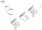
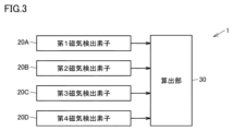
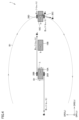
図1は、本発明の一実施形態に係る電流センサの構成を一方向から示す斜視図である。図2は、本発明の一実施形態に係る電流センサの構成を他方向から示す斜視図である。図3は、本発明の一実施形態に係る電流センサの構成を示すブロック図である。図4は、本発明の一実施形態に係る電流センサの構成を示し、かつ、第1磁界を模式的に示す断面図である。
図1から図4に示すように、本発明の一実施形態に係る電流センサ1は、第1バスバ10Aと、第2バスバ10Bと、第3バスバ10Cと、第1磁気検出素子20Aと、第2磁気検出素子20Bと、第3磁気検出素子20Cと、第4磁気検出素子20Dと、算出部30とを備えている。
図1、図2および図4に示すように、第1バスバ10Aは、第1方向DR1に沿って直線状に延びている。
第1バスバ10Aには、第1方向DR1に第1電流が流れている。第1電流は、交流電流である。このため、第1方向DR1における第1電流の電流値(I1)は、正の値または負の値をとり得る。第1電流が流れた際には、第1磁界B1が第1バスバ10Aの周囲に生じる。
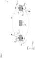
図5は、本発明の一実施形態に係る電流センサの構成を示し、かつ、第2磁界を模式的に示す断面図である。図1、図2および図5に示すように、第2バスバ10Bは、第1方向DR1に沿って直線状に延びている。第2バスバ10Bは、第2方向DR2において第1バスバ10Aと並んでいる。第2方向DR2は、第1方向DR1に直交する方向である。
第2バスバ10Bには、第1方向DR1に第2電流が流れている。第2電流は、交流電流である。このため、第1方向DR1における第2電流の電流値(I2)は、正の値または負の値をとり得る。第2電流が流れた際には、第2磁界B2が第2バスバ10Bの周囲に生じる。
図6は、本発明の一実施形態に係る電流センサの構成を示し、かつ、第3磁界を模式的に示す断面図である。図1、図2、および図6に示すように、第3バスバ10Cは、第1方向DR1に沿って直線状に延びている。第3バスバ10Cは、第2方向DR2において第2バスバ10Bと並んでいる。第3バスバ10Cは、第2バスバ10Bとの距離が、第1バスバ10Aと第2バスバ10Bとの距離に等しくなるように位置している。
第3バスバ10Cには、第1方向DR1に第3電流が流れている。第3電流は、交流電流である。このため、第1方向DR1における第3電流の電流値(I3)は、正の値または負の値をとり得る。第3電流が流れた際には、第3磁界B3が第3バスバ10Cの周囲に生じる。
第1バスバ10A、第2バスバ10Bおよび第3バスバ10Cは、3相3線式のバスバである。第1電流、第2電流、および、第3電流は、三相交流を構成している。第1電流、第2電流、および、第3電流は、第1方向DR1において、振幅が等しく互いに位相が120°ずつずれた交流電流を構成している。すなわち、第1バスバ10Aを第1方向DR1に流れる第1電流の電流値(I1)、第2バスバ10Bを第1方向DR1に流れる第2電流の電流値(I2)、および、第3バスバ10Cを第1方向DR1に流れる第3電流の電流値(I3)においては、I1+I2+I3=0の関係が成立している。たとえば、第1電流がU相の交流電流、第2電流がV相の交流電流、第3電流がW相の交流電流であってもよい。
図2、図4~図6に示すように、第1磁気検出素子20Aは、第3方向DR3において第1バスバ10Aと並んでいる。第3方向DR3は、第1方向DR1および第2方向DR2の両方に直交する方向である。第1磁気検出素子20Aは、第1バスバ10Aと離隔している。第1磁気検出素子20Aは、第2方向DR2または第2方向DR2の反対方向に向いた感度軸を有している。
図1、図4~図6に示すように、第2磁気検出素子20Bは、第3方向DR3において第1バスバ10Aと並んでいる。第2磁気検出素子20Bは、第1バスバ10Aから見て第1磁気検出素子20Aの反対側に位置している。第2磁気検出素子20Bは、第1バスバ10Aとの距離が、第1バスバ10Aと第1磁気検出素子20Aとの距離に等しくなるように位置している。第2磁気検出素子20Bは、第1バスバ10Aと離隔している。第2磁気検出素子20Bは、第1磁気検出素子20Aの感度軸の方向と反対方向に向いた感度軸を有している。
図2、図4~図6に示すように、第3磁気検出素子20Cは、第3方向DR3において第3バスバ10Cと並んでいる。第3磁気検出素子20Cは、第2方向DR2において第1磁気検出素子20Aと並んでいる。第3磁気検出素子20Cは、第3バスバ10Cと離隔している。第3磁気検出素子20Cは、第1磁気検出素子20Aの感度軸の方向と同じ方向を向く感度軸を有している。
図1、図4~図6に示すように、第4磁気検出素子20Dは、第3方向DR3において第3バスバ10Cと並んでいる。第4磁気検出素子20Dは、第2方向DR2において第2磁気検出素子20Bと並んでいる。第4磁気検出素子20Dは、第3バスバ10Cと離隔している。第4磁気検出素子20Dは、第2磁気検出素子20Bの感度軸の方向と同じ方向を向く感度軸を有している。
なお、本実施形態においては、第1バスバ10Aと第2バスバ10Bとの間、第2バスバ10Bと第3バスバ10Cとの間、第1磁気検出素子20Aと第2バスバ10Bとの間、第2磁気検出素子20Bと第2バスバ10Bとの間、第3磁気検出素子20Cと第2バスバ10Bとの間、第4磁気検出素子20Dと第2バスバ10Bとの間には、透磁率の高い磁性材料などからなる磁気遮蔽板、および、磁場を集磁するための柔磁性体などからなる磁性体コアは設けられていない。これにより、本実施形態に係る電流センサ1は、全体のサイズを小型化できる。
次に、各磁気検出素子に印加される磁界成分について説明する。図7は、本発明の一実施形態に係る電流センサの構成を示し、各々の磁気検出素子に印加される外部磁界成分を模式的に示す断面図である。第1磁気検出素子20Aは、第2方向DR2に印加された磁界成分に応じた第1出力値(V1)を出力する。本実施形態においては、上述のように各磁気検出素子の間および各バスバの間に、磁気遮蔽板および磁性体コアが設けられていない。このため、第1出力値(V1)は、磁界成分B11x(図4参照)と、磁界成分B21x(図5参照)と、磁界成分B31x(図6参照)と、外部磁界成分BE1x(図7参照)との和に応じて出力される。
磁界成分B11xは、第1磁界B1による、第1磁気検出素子20Aにおける磁束密度ベクトルB11の第2方向DR2(x方向)の成分である。磁界成分B21xは、第2磁界B2による、第1磁気検出素子20Aにおける磁束密度ベクトルB21の第2方向DR2(x方向)の成分である。磁界成分B31xは、第3磁界B3による、第1磁気検出素子20Aにおける磁束密度ベクトルB31の第2方向DR2(x方向)の成分である。外部磁界成分BE1xは、第1磁気検出素子20A、第2磁気検出素子20B、第3磁気検出素子20C、および、第4磁気検出素子20Dに一様に印加される外部磁界の、第1磁気検出素子20Aの感度軸方向における成分である。
第2磁気検出素子20Bは、第2方向DR2に印加された磁界成分に応じた第2出力値(V2)を出力する。本実施形態においては、上述のように各磁気検出素子の間および各バスバの間に、磁気遮蔽板および磁性体コアが設けられていない。このため、第2出力値(V2)は、磁界成分B12x(図4参照)と、磁界成分B22x(図5参照)と、磁界成分B32x(図6参照)と、外部磁界成分BE2x(図7参照)との和に応じて出力される。
磁界成分B12xは、第1磁界B1による、第2磁気検出素子20Bにおける磁束密度ベクトルB12の第2方向DR2(x方向)の成分である。磁界成分B22xは、第2磁界B2による、第2磁気検出素子20Bにおける磁束密度ベクトルB22の第2方向DR2(x方向)の成分である。磁界成分B32xは、第3磁界B3による、第2磁気検出素子20Bにおける磁束密度ベクトルB32の第2方向DR2(x方向)の成分である。外部磁界成分BE2xは、第1磁気検出素子20A、第2磁気検出素子20B、第3磁気検出素子20C、および、第4磁気検出素子20Dに一様に印加される外部磁界の、第2磁気検出素子20Bの感度軸方向における成分である。
第3磁気検出素子20Cは、第2方向DR2に印加された磁界成分に応じた第3出力値(V3)を出力する。本実施形態においては、上述のように各磁気検出素子の間および各バスバの間に、磁気遮蔽板および磁性体コアが設けられていない。このため、第3出力値(V3)は、磁界成分B13x(図4参照)と、磁界成分B23x(図5参照)と、磁界成分B33x(図6参照)と、外部磁界成分BE3x(図7参照)との和に応じて出力される。
磁界成分B13xは、第1磁界B1による、第3磁気検出素子20Cにおける磁束密度ベクトルB13の第2方向DR2(x方向)の成分である。磁界成分B23xは、第2磁界B2による、第3磁気検出素子20Cにおける磁束密度ベクトルB23の第2方向DR2(x方向)の成分である。磁界成分B33xは、第3磁界B3による、第3磁気検出素子20Cにおける磁束密度ベクトルB33の第2方向DR2(x方向)の成分である。外部磁界成分BE3xは、第1磁気検出素子20A、第2磁気検出素子20B、第3磁気検出素子20C、および、第4磁気検出素子20Dに一様に印加される外部磁界の、第3磁気検出素子20Cの感度軸方向における成分である。
第4磁気検出素子20Dは、第2方向DR2に印加された磁界成分に応じた第4出力値(V4)を出力する。本実施形態においては、上述のように各磁気検出素子の間および各バスバの間に、磁気遮蔽板および磁性体コアが設けられていない。このため、第4出力値(V4)は、磁界成分B14x(図4参照)と、磁界成分B24x(図5参照)と、磁界成分B34x(図6参照)と、外部磁界成分BE4x(図7参照)との和に応じて出力される。
磁界成分B14xは、第1磁界B1による、第4磁気検出素子20Dにおける磁束密度ベクトルB14の第2方向DR2(x方向)の成分である。磁界成分B24xは、第2磁界B2による、第4磁気検出素子20Dにおける磁束密度ベクトルB24の第2方向DR2(x方向)の成分である。磁界成分B34xは、第3磁界B3による、第4磁気検出素子20Dにおける磁束密度ベクトルB34の第2方向DR2(x方向)の成分である。外部磁界成分BE4xは、第1磁気検出素子20A、第2磁気検出素子20B、第3磁気検出素子20C、および、第4磁気検出素子20Dに一様に印加される外部磁界の、第4磁気検出素子20Dの感度軸方向における成分である。
第1磁気検出素子20A、第2磁気検出素子20B、第3磁気検出素子20Cおよび第4磁気検出素子20Dの少なくとも1つは、少なくとも2つ以上の磁気抵抗素子からなる回路を有していてもよい。第1磁気検出素子20A、第2磁気検出素子20B、第3磁気検出素子20Cおよび第4磁気検出素子20Dの各々のいずれもが、少なくとも2つ以上の磁気抵抗素子からなる回路を有していてもよい。少なくとも2つ以上の磁気抵抗素子からなる回路は、2つの磁気抵抗素子からなるハーフブリッジ回路であってもよいし、4つの磁気抵抗素子からなるホイートストンブリッジ型のブリッジ回路であってもよい。
また、上記磁気抵抗素子は、トンネル型磁気抵抗(Tunnel Magneto Resistance(TMR))素子、巨大磁気抵抗(Giant Magneto Resistance(GMR))素子、または、異方性磁気抵抗(Anisotropic Magnetic Resistance(AMR))素子のいずれであってもよい。
第1磁気検出素子20A、第2磁気検出素子20B、第3磁気検出素子20Cおよび第4磁気検出素子20Dのうちの少なくとも1つが、ホール素子を有してもよい。第1磁気検出素子20A、第2磁気検出素子20B、第3磁気検出素子20Cおよび第4磁気検出素子20Dの各々のいずれもが、ホール素子を有してもよい。
ただし、第1磁気検出素子20A、第2磁気検出素子20B、第3磁気検出素子20Cおよび第4磁気検出素子20Dがどのような種類の素子であっても、これらの素子は、第2方向DR2(x方向)に印加された磁界成分に対して同様の係数を乗じることで算出される出力値を出力することが好ましい。
算出部30は、第1出力値(V1)、第2出力値(V2)、第3出力値(V3)および第4出力値(V4)、ならびに、下記式(1)、式(2)および式(3)に基づき、第1電流の電流値(I1)、第2電流の電流値(I2)、および、第3電流の電流値(I3)を算出可能に構成されている。

まず、上記式(1)について説明する。上述したように、第1出力値(V1)は、磁界成分B11xと、磁界成分B21xと、磁界成分B31x(と、外部磁界成分BE1xとの和に応じて出力され、第2出力値(V2)は、磁界成分B12xと、磁界成分B22xと、磁界成分B32xと、外部磁界成分BE2xとの和に応じて出力されるため、(V1+V2)は、下記式(4)のように展開することができる。よって、算出部30は、上記式(1)に基づいて、第1電流の電流値(I1)を算出可能に構成される。
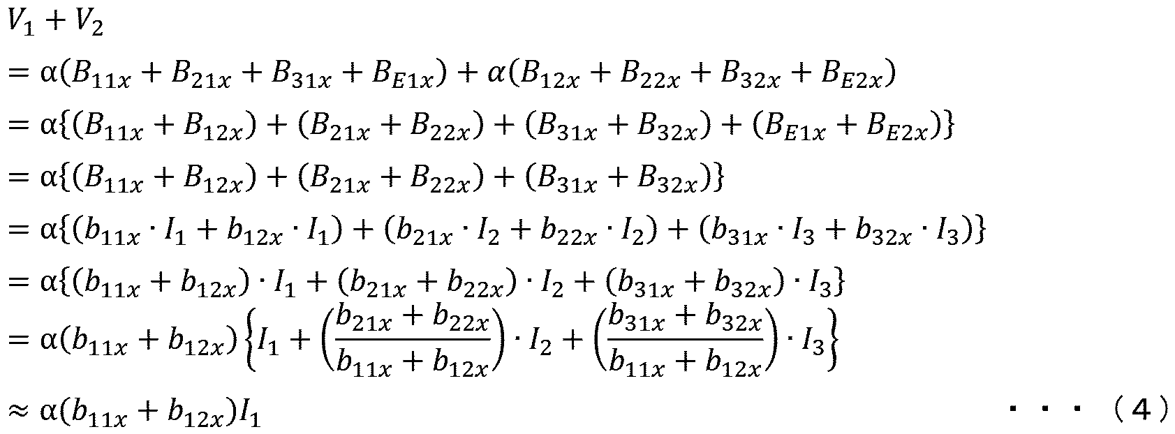
なお、上記式(4)(および後述する式(5)および式(6))において、αは係数であり、bnmx(nは1から3の整数、mは1から4の整数)は、本実施形態において、第1バスバ10A、第2バスバ10B、第3バスバ10C、第1磁気検出素子20A、第2磁気検出素子20B、第3磁気検出素子20Cおよび、第4磁気検出素子20Dの構成によって定まる定数である。
上記式(4)においては、BE1x+BE2xが、0に変換されている。この変換は、第1磁気検出素子20Aおよび第2磁気検出素子20Bの感度軸方向が互いに反対方向を向いており、これにより、外部磁界成分BE1xおよび外部磁界成分BE1xが、互いに絶対値の等しい値であって、正負が逆転している値をとるためである。さらに、上記式(4)においては、{(b21x+b22x)/(b11x+b12x)}および{(b31x+b32x)/(b11x+b12x)}が0に近似されている。これは、(b11x+b12x)と比較して、(b21x+b22x)および(b31x+b32x)が非常に小さい値となるからである。より具体的には、第1磁気検出素子20Aおよび第2磁気検出素子20Bと第2バスバ10Bとの距離(図5参照)、および、第1磁気検出素子20Aおよび第2磁気検出素子20Bと第3バスバ10Cとの距離(図6参照)は、第1磁気検出素子20Aおよび第2磁気検出素子20Bと第1バスバ10Aとの距離(図4参照)と比較して非常に小さいからである。さらには、第1磁気検出素子20Aおよび第2磁気検出素子20Bの感度軸方向は、第1磁界B1のベクトルの向きに対して平行に近いが(図4参照)、第2磁界B2および第3磁界B3の各々のベクトルの向きに対しては直交に近くなる(図5および図6参照)からである。
さらに、上記式(3)も同様にして、下記式(5)のように展開することができる。このため、算出部30は、上記式(3)に基づいて、第3電流の電流値(I3)を算出可能に構成される。
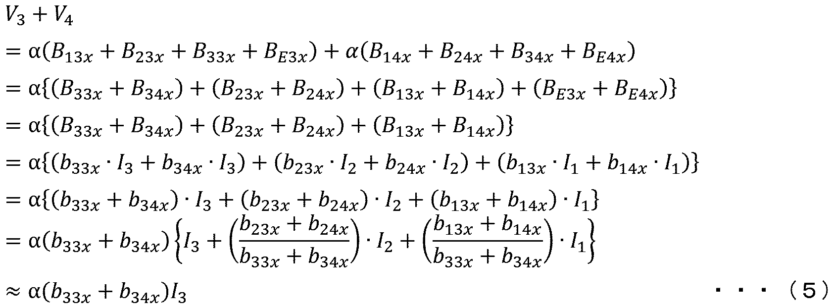
上記式(5)においては、BE3x+BE4xが、0に変換されている。この変換は、第3磁気検出素子20Cおよび第4磁気検出素子20Dの感度軸方向が互いに反対方向を向いており、これにより、外部磁界成分BE3xおよび外部磁界成分BE4xが、互いに絶対値の等しい値であって、正負が逆転している値をとるためである。さらに、上記式(4)においては、{(b23x+b24x)/(b33x+b34x)}および{(b13x+b14x)/(b33x+b34x)}が0に近似されている。これは、(b33x+b34x)と比較して、(b23x+b24x)および(b13x+b14x)が非常に小さい値となるからである。より具体的には、第3磁気検出素子20Cおよび第4磁気検出素子20Dと第2バスバ10Bとの距離(図5参照)、および、第3磁気検出素子20Cおよび第4磁気検出素子20Dと第1バスバ10Aとの距離(図4参照)は、第3磁気検出素子20Cおよび第4磁気検出素子20Dと第1バスバ10Aとの距離(図4参照)と比較して非常に小さいからである。さらには、第3磁気検出素子20Cおよび第4磁気検出素子20Dの感度軸方向は、第3磁界B3のベクトルの向きに対して平行に近いが(図6参照)、第2磁界B2および第1磁界B1の各々のベクトルの向きに対しては直交に近くなる(図5および図4参照)からである。
ここで、図4および図6に示すように、各磁気検出素子および第1バスバ10Aおよび第3バスバ10Cが上述の位置関係にあり、かつ、第1バスバ10Aおよび第3バスバ10Cの感度軸の方向が上述の方向であることにより、b11x、b12x、b33x、b34xの値は、互いに等しくなる。
したがって、下記式(2)に対応するように、(V1+V2+V3+V4)は、上記式(4)および(5)に基づいて下記式(6)のように展開することができる。よって、算出部30は、上記式(2)に基づいて、第2電流の電流値(I2)を算出可能に構成される。
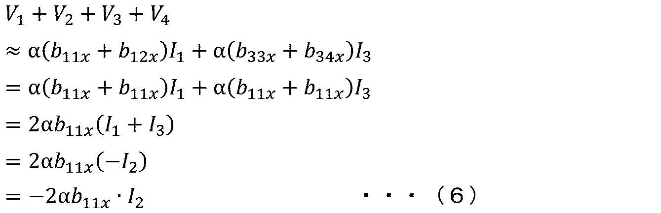
なお、上記式(6)においては、I1+I3が、-I2に変換されている。この変換が可能となるのは、上述したようにI1+I2+I3=0の関係が成立しているためである。
次に、本実施形態に係る電流センサ1の回路構成を説明するが、本実施形態に係る電流センサ1の回路構成は、以下の構成に限定されない。
図8は、本発明の一実施形態に係る電流センサの回路構成を概略的に示す回路図である。図8に示すように、本実施形態において、第1磁気検出素子20A、第2磁気検出素子20B、第3磁気検出素子20Cおよび第4磁気検出素子20Dは、それぞれ、4つのトンネル型磁気抵抗素子21からなるホイートストンブリッジ型のブリッジ回路を有する。
第1磁気検出素子20Aの検出信号は、第1アンプ22Aを介して、第1出力値(V1)を示す第1電圧信号として出力される。第2磁気検出素子20Bの検出信号は、第2アンプ22Bを介して、第2出力値(V2)を示す第2電圧信号として出力される。第3磁気検出素子20Cの検出信号は、第3アンプ22Cを介して、第3出力値(V3)を示す第3電圧信号として出力される。第4磁気検出素子20Dの検出信号は、第4アンプ22Dを介して、第4出力値(V4)を示す第4電圧信号として出力される。第1アンプ22A、第2アンプ22B、第3アンプ22Cおよび第4アンプ22Dは、それぞれ、差動増幅をするオペアンプにより構成される。
算出部30は、アンプ等の回路素子を接続して構成されるアナログ回路であり、第1出力値(V1)を示す第1電圧信号、第2出力値(V2)を示す第2電圧信号、第3出力値(V3)を示す第3電圧信号、第4出力値(V4)を示す第4電圧信号が入力され、これらの入力信号に応じて、第1電流の電流(検出)値(I1)に対応する第1出力電圧信号(V1OUT)、第2電流の電流(検出)値(I2)に対応する第2出力電圧信号(V2OUT)、第3電流の電流(検出)値(I3)に対応する第3出力電圧信号(V3OUT)を出力する。
算出部30は、第1加算増幅器31A、第2加算増幅器31B、および、第3加算増幅器31Cを有する。第1加算増幅器31Aには、第1出力値(V1)を示す第1電圧信号および第2出力値(V2)を示す第2電圧信号が入力される。第1加算増幅器31Aは、第1出力電圧信号(V1OUT)を出力する。ここで、本実施形態においては、上記式(1)が成立するため、算出部30は、第1出力電圧信号(V1OUT)を、第1電流の電流(検出)値(I1)に対応する電圧信号として出力することができる。
第2加算増幅器31Bには、第1出力値(V1)を示す第1電圧信号、第2出力値(V2)を示す第2電圧信号、第3出力値(V3)を示す第3電圧信号、および、第4出力値(V4)を示す第4電圧信号が入力される。第2加算増幅器31Bは、第2出力電圧信号(V2OUT)を出力する。ここで、本実施形態においては、上記式(2)が成立するため、算出部30は、第2出力電圧信号(V2OUT)を、第2電流の電流(検出)値(I2)に対応する電圧信号として出力することができる。
第3加算増幅器31Cには、第3出力値(V3)を示す第3電圧信号および第4出力値(V4)を示す第4電圧信号が入力される。第3加算増幅器31Cは、第3出力電圧信号(V3OUT)を出力する。ここで、本実施形態においては、上記式(3)が成立するため、算出部30は、第3出力電圧信号(V3OUT)を、第3電流の電流(検出)値(I3)に対応する電圧信号として出力することができる。
以上説明したように、本実施形態に係る電流センサ1においては、算出部30が、上記式(1)、式(2)および式(3)に基づき、第1電流の電流値(I1)、第2電流の電流値(I2)、および、第3電流の電流値(I3)を算出可能に構成されている。これにより、本実施形態に係る電流センサ1においては、たとえば上述のように算出部30を3つの加算増幅器によって各電流値に対応する信号を直接に出力することが可能になり、全体のサイズが小型化され、特に、第2電流の電流値(I2)に対応する電圧信号を出力するための処理段数が少なくなることで応答性が向上し得る。さらには、上記式(4)~(6)に示されるように、各磁気検出素子に印加される外部磁界成分は、各電流値の算出の過程において相殺される。よって、一様な外部磁場の影響が抑制された、電流センサ1を提供できる。
上述した実施形態の説明において、組み合わせ可能な構成を相互に組み合わせてもよい。
今回開示された実施形態はすべての点で例示であって制限的なものではないと考えられるべきである。本発明の範囲は上記した説明ではなくて請求の範囲によって示され、請求の範囲と均等の意味および範囲内でのすべての変更が含まれることが意図される。
1 電流センサ、10A 第1バスバ、10B 第2バスバ、10C 第3バスバ、20A 第1磁気検出素子、20B 第2磁気検出素子、20C 第3磁気検出素子、20D 第4磁気検出素子、21 トンネル型磁気抵抗素子、22A 第1アンプ、22B 第2アンプ、22C 第3アンプ、22D 第4アンプ、30 算出部、31A 第1加算増幅器、31B 第2加算増幅器、31C 第3加算増幅器。
Claims (5)
- 第1方向に沿って延びる第1バスバと、
前記第1方向に沿って延び、前記第1方向に直交する第2方向において前記第1バスバと並ぶ第2バスバと、
前記第1方向に沿って延び、前記第2方向において前記第2バスバと並び、かつ、前記第2バスバとの距離が、前記第1バスバと前記第2バスバとの距離に等しくなるように位置する、第3バスバと、
前記第1方向および前記第2方向の両方に直交する第3方向において前記第1バスバと並び、前記第2方向または前記第2方向の反対方向に向いた感度軸を有し、前記第2方向に印加された磁界成分に応じた第1出力値(V1)を出力する、第1磁気検出素子と、
前記第3方向において前記第1バスバと並び、かつ、前記第1バスバから見て前記第1磁気検出素子の反対側において、前記第1バスバとの距離が、前記第1バスバと前記第1磁気検出素子との距離に等しくなるように位置し、前記第1磁気検出素子の感度軸の方向と反対方向に向いた感度軸を有し、前記第2方向に印加された磁界成分に応じた第2出力値(V2)を出力する、第2磁気検出素子と、
前記第3方向において前記第3バスバと並び、かつ、前記第2方向において前記第1磁気検出素子と並び、前記第1磁気検出素子の感度軸の方向と同じ方向を向く感度軸を有し、前記第2方向に印加された磁界成分に応じた第3出力値(V3)を出力する、第3磁気検出素子と、
前記第3方向において前記第3バスバと並び、かつ、前記第2方向において前記第2磁気検出素子と並び、前記第2磁気検出素子の感度軸の方向と同じ方向を向く感度軸を有し、前記第2方向に印加された磁界成分に応じた第4出力値(V4)を出力する、第4磁気検出素子と、
前記第1出力値(V1)、前記第2出力値(V2)、前記第3出力値(V3)および前記第4出力値(V4)に基づき、前記第1バスバを前記第1方向に流れる第1電流の電流値(I1)、前記第2バスバを前記第1方向に流れる第2電流の電流値(I2)、および、前記第3バスバを前記第1方向に流れる第3電流の電流値(I3)を算出する算出部とを備え、
前記第1電流、前記第2電流、および、前記第3電流は、三相交流を構成しており、
前記算出部は、下記式(1)、式(2)および式(3)

に基づき、前記第1電流の電流値(I1)、前記第2電流の電流値(I2)、および、前記第3電流の電流値(I3)を算出可能に構成されている、電流センサ。 - 前記第1磁気検出素子、前記第2磁気検出素子、前記第3磁気検出素子および前記第4磁気検出素子のうちの少なくとも1つが、少なくとも2つ以上のトンネル型磁気抵抗素子からなる回路を有する、請求項1に記載の電流センサ。
- 前記第1磁気検出素子、前記第2磁気検出素子、前記第3磁気検出素子および前記第4磁気検出素子のうちの少なくとも1つが、少なくとも2つ以上の巨大磁気抵抗素子からなる回路を有する、請求項1に記載の電流センサ。
- 前記第1磁気検出素子、前記第2磁気検出素子、前記第3磁気検出素子および前記第4磁気検出素子のうちの少なくとも1つが、少なくとも2つ以上の異方性磁気抵抗素子からなる回路を有する、請求項1に記載の電流センサ。
- 前記第1磁気検出素子、前記第2磁気検出素子、前記第3磁気検出素子および前記第4磁気検出素子のうちの少なくとも1つが、ホール素子を有する、請求項1に記載の電流センサ。
Applications Claiming Priority (2)
| Application Number | Priority Date | Filing Date | Title |
|---|---|---|---|
| JP2023-092245 | 2023-06-05 | ||
| JP2023092245 | 2023-06-05 |
Publications (1)
| Publication Number | Publication Date |
|---|---|
| WO2024252947A1 true WO2024252947A1 (ja) | 2024-12-12 |
Family
ID=93795883
Family Applications (1)
| Application Number | Title | Priority Date | Filing Date |
|---|---|---|---|
| PCT/JP2024/019063 Ceased WO2024252947A1 (ja) | 2023-06-05 | 2024-05-23 | 電流センサ |
Country Status (1)
| Country | Link |
|---|---|
| WO (1) | WO2024252947A1 (ja) |
Citations (6)
| Publication number | Priority date | Publication date | Assignee | Title |
|---|---|---|---|---|
| JP2005195427A (ja) * | 2004-01-06 | 2005-07-21 | Asahi Kasei Electronics Co Ltd | 電流測定装置、電流測定方法および電流測定プログラム |
| JP2006112968A (ja) * | 2004-10-15 | 2006-04-27 | Toyota Motor Corp | 電流検出装置 |
| JP2016133498A (ja) * | 2015-01-22 | 2016-07-25 | 日本特殊陶業株式会社 | 電流電力センサ |
| CN109374940A (zh) * | 2018-11-30 | 2019-02-22 | 无锡乐尔科技有限公司 | 铜排型导线的电流测量方法及装置 |
| JP2022035655A (ja) * | 2020-08-21 | 2022-03-04 | 富士電機株式会社 | 電力変換装置及び電流検出装置 |
| WO2023053792A1 (ja) * | 2021-09-29 | 2023-04-06 | 株式会社村田製作所 | 電流センサ、その補正方法、および、複数の電流センサの補正方法 |
-
2024
- 2024-05-23 WO PCT/JP2024/019063 patent/WO2024252947A1/ja not_active Ceased
Patent Citations (6)
| Publication number | Priority date | Publication date | Assignee | Title |
|---|---|---|---|---|
| JP2005195427A (ja) * | 2004-01-06 | 2005-07-21 | Asahi Kasei Electronics Co Ltd | 電流測定装置、電流測定方法および電流測定プログラム |
| JP2006112968A (ja) * | 2004-10-15 | 2006-04-27 | Toyota Motor Corp | 電流検出装置 |
| JP2016133498A (ja) * | 2015-01-22 | 2016-07-25 | 日本特殊陶業株式会社 | 電流電力センサ |
| CN109374940A (zh) * | 2018-11-30 | 2019-02-22 | 无锡乐尔科技有限公司 | 铜排型导线的电流测量方法及装置 |
| JP2022035655A (ja) * | 2020-08-21 | 2022-03-04 | 富士電機株式会社 | 電力変換装置及び電流検出装置 |
| WO2023053792A1 (ja) * | 2021-09-29 | 2023-04-06 | 株式会社村田製作所 | 電流センサ、その補正方法、および、複数の電流センサの補正方法 |
Similar Documents
| Publication | Publication Date | Title |
|---|---|---|
| US10571303B2 (en) | Redundant fault detection device and method | |
| EP1654552B1 (en) | Method and apparatus for measuring a magnetic field by using a hall-sensor | |
| JP2002243766A (ja) | 電流センサ | |
| US12044529B2 (en) | Magnetic sensor including a magnetoresistance element and sensor system | |
| JP2011027683A (ja) | 磁気センサ | |
| JP2013134202A (ja) | 電流センサ | |
| US7821252B2 (en) | Three-phase current sensor | |
| JP2016133498A (ja) | 電流電力センサ | |
| JP4873709B2 (ja) | 電流センサ | |
| WO2024252947A1 (ja) | 電流センサ | |
| JP2016148597A (ja) | 電流センサ | |
| EP4455686A1 (en) | Stepped copper-bar current measurement apparatus | |
| JP2026021527A (ja) | 磁気センサおよび磁気測定方法 | |
| WO2024190581A1 (ja) | 電流センサ | |
| US20260056268A1 (en) | Current sensor | |
| KR102693270B1 (ko) | 고자기장의 2 차원 감지를 위한 자기저항 기반 감지 회로 | |
| WO2016002500A1 (ja) | 電流センサ | |
| JP2005207791A (ja) | 電流測定装置および電流測定方法 | |
| JP6881937B2 (ja) | 電流センサ | |
| JP2016142655A (ja) | 電流測定装置 | |
| JP7819810B2 (ja) | 電流センサ | |
| US20250224428A1 (en) | Current sensor | |
| JP2016142652A (ja) | 電力センサー | |
| JPS5868615A (ja) | 磁気式ロ−タリ・エンコ−ダの出力回路 | |
| CN114062755B (zh) | 电流传感器 |
Legal Events
| Date | Code | Title | Description |
|---|---|---|---|
| 121 | Ep: the epo has been informed by wipo that ep was designated in this application |
Ref document number: 24819179 Country of ref document: EP Kind code of ref document: A1 |
|
| NENP | Non-entry into the national phase |
Ref country code: DE |