WO2024252989A1 - Élément de modulation optique à semi-conducteur - Google Patents
Élément de modulation optique à semi-conducteur Download PDFInfo
- Publication number
- WO2024252989A1 WO2024252989A1 PCT/JP2024/019585 JP2024019585W WO2024252989A1 WO 2024252989 A1 WO2024252989 A1 WO 2024252989A1 JP 2024019585 W JP2024019585 W JP 2024019585W WO 2024252989 A1 WO2024252989 A1 WO 2024252989A1
- Authority
- WO
- WIPO (PCT)
- Prior art keywords
- layer
- modulation element
- optical
- optical modulation
- type
- Prior art date
- Legal status (The legal status is an assumption and is not a legal conclusion. Google has not performed a legal analysis and makes no representation as to the accuracy of the status listed.)
- Ceased
Links
Images

Classifications
-
- G—PHYSICS
- G02—OPTICS
- G02F—OPTICAL DEVICES OR ARRANGEMENTS FOR THE CONTROL OF LIGHT BY MODIFICATION OF THE OPTICAL PROPERTIES OF THE MEDIA OF THE ELEMENTS INVOLVED THEREIN; NON-LINEAR OPTICS; FREQUENCY-CHANGING OF LIGHT; OPTICAL LOGIC ELEMENTS; OPTICAL ANALOGUE/DIGITAL CONVERTERS
- G02F1/00—Devices or arrangements for the control of the intensity, colour, phase, polarisation or direction of light arriving from an independent light source, e.g. switching, gating or modulating; Non-linear optics
- G02F1/01—Devices or arrangements for the control of the intensity, colour, phase, polarisation or direction of light arriving from an independent light source, e.g. switching, gating or modulating; Non-linear optics for the control of the intensity, phase, polarisation or colour
- G02F1/015—Devices or arrangements for the control of the intensity, colour, phase, polarisation or direction of light arriving from an independent light source, e.g. switching, gating or modulating; Non-linear optics for the control of the intensity, phase, polarisation or colour based on semiconductor elements having potential barriers, e.g. having a PN or PIN junction
- G02F1/017—Structures with periodic or quasi periodic potential variation, e.g. superlattices, quantum wells
Definitions
- the present invention relates to an optical modulation element, and more specifically to an n-i-p-n type optical modulation element.
- MZMs Mach-Zehnder modulators
- Non-Patent Document 1 n-p-i-n structures or n-i-p-n structures have been proposed. These structures focus on the fact that the factor limiting the increase in speed of semiconductor optical modulators is the high resistance characteristics of the semiconductor doped layer. Instead of p-doped layers, which have a resistivity roughly one order of magnitude higher at the same concentration, n-doped layers are placed above and below the layer structure to achieve both wideband characteristics and low drive voltage characteristics (Non-Patent Document 1).
- Figure 1 shows the layer structure and band diagram of a semiconductor optical modulation element of the prior art.
- Figure 1(a) shows the layer structure 100 of the cross section of an optical waveguide that performs the modulation operation of the MZM. A part is cut out and shown in a schematic diagram, focusing on the configuration of the semiconductor layers with an n-i-p-n structure.
- Figure 1(b) shows a band diagram corresponding to the n-i-p-n structure in (a).
- the terms optical modulator and optical modulation element mean the same thing.
- an n-type cladding layer 12 As shown in FIG. 1A, from the bottom where the InP substrate (not shown) is located, an n-type cladding layer 12, a p-type diffusion stop layer 18, a non-doped layer (i-layer) including multiple layers including a core layer of an optical waveguide, and an n-type cladding layer 17 are laminated.
- the non-doped layer includes, from the substrate side, a first buffer layer 14, an MQW layer 15 having a multi-quantum well (MQW) structure and functioning as a core layer, and a second buffer layer 16.
- MQW multi-quantum well
- an n-layer, an i-layer, a p-layer, and an n-layer are configured in that order, and this is called an n-i-p-n structure.
- Only the MQW layer 15 in the i-layer functions as the optical waveguide core.
- the non-doped i-layer including multiple layers determines the electrical capacitance (capacitor) as described later.
- the p-type doped layer is shown as the electron barrier layer 13.
- Zn, Be, C, etc. are used as dopants for the electron barrier layer 13.
- MOVPE method which is used to create compound semiconductor crystals and is also suitable for mass production, Zn is used as the dopant in most cases.
- Zn dopants are known to have a very large diffusion coefficient, and how to suppress Zn diffusion is an important issue in the design of optical devices such as laser diodes and optical modulators.
- an effective method of suppressing Zn diffusion is to form a heterointerface with a different band gap between a Zn-doped layer and a non-doped core layer.
- Zn diffusion from a p-InP cladding layer can be prevented by inserting adjacent non-doped InGaAsP layers, InAlGaAs layers, InAlAs layers, etc., which have a higher saturation concentration than InP.
- InGaAsP is expected to have a high Zn diffusion prevention effect because it shows the highest saturation concentration characteristics.
- a diffusion stop layer 18 made of InGaAsP is provided between the first n-type cladding layer 12 and the first buffer layer 14 as a layer to prevent the above-mentioned diffusion of Zn. Since the InGaAsP layer contains both As and P as group V elements, it is often used as an intermediate layer to switch from an InAlAs layer to an InP layer in epitaxial growth. By forming this intermediate layer between each layer, crystal defects can be reduced.
- the band diagram in FIG. 1(b) corresponds to the layer configuration of the semiconductor optical modulation element with the n-i-p-n structure described above.
- the electron barrier layer 13 is shown like a dam wall, with a doping concentration and thickness that are such that no large dark current flows when a reverse bias is applied.
- the diffusion stop layer 18 described above is also shown in the band diagram as a relatively thin region adjacent to the electron barrier layer 13.
- the slope of each part in the band diagram corresponds to the electric field strength applied to that part (layer); if the band slope is steep, a strong electric field is applied, and if the band slope is gentle, a weak electric field is applied.
- the present invention was made in consideration of these problems, and its purpose is to reduce the wavelength dependency in the modulation output performance of n-i-p-n type optical modulation elements.
- One aspect of the present invention is a Mach-Zehnder type semiconductor optical modulation element having an input optical waveguide, two interference optical waveguides branched from the input optical waveguide and having a core refractive index modulated by an electric signal, and an output optical waveguide for the modulated light combined from the two interference optical waveguides, each of which has a first n-type cladding layer, a p-type electron barrier layer, a first buffer layer, a multiple quantum well layer constituting the core, a second buffer layer, and a second n-type cladding layer arranged in this order from the InP semiconductor crystal substrate upward on a substrate surface equivalent to the (100) surface of the semi-insulating InP semiconductor crystal substrate, and the first buffer layer is a semiconductor optical modulation element containing only As as a group V element.
- the second buffer layer can contain P and As as group V elements.
- the dopant of the p-type electron barrier layer can be carbon.
- the constituent material between the p-type electron barrier layer and the multiple quantum well layer can be composed of a single composition, and the composition can be the same composition as the p-type electron barrier layer of the multiple quantum well layer.
- FIG. 1 is a diagram showing a layer structure and a band diagram of a conventional nipn type optical modulation element.
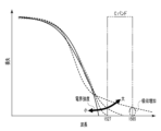
- FIG. 13 is a diagram showing the electric field strength dependence of the absorption spectrum of an InGaAsP layer.
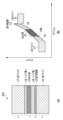
- 1A and 1B are diagrams showing a layer structure and a band diagram of an nipn type optical modulation element according to the present disclosure.
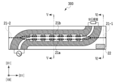
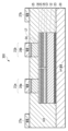
- 1 is a diagram showing a top view of a semiconductor optical modulation device according to a first embodiment of the present disclosure; 3 is a diagram showing a cross-sectional structure of a refractive index modulation region of the semiconductor optical modulation element of Example 1.
- FIG. 2 is a diagram showing a cross-sectional structure of an input optical waveguide of the semiconductor optical modulation element of Example 1.
- This paper discloses an InP optical modulation element having an n-i-p-n heterostructure.
- we will first confirm the large wavelength dependency that occurs in the performance of the optical modulator in a semiconductor optical modulation element with an n-i-p-n structure of the prior art. We will then explain the configuration and operation of the optical modulation element disclosed herein.
- the material of the diffusion stop layer 18 shown in Figure 1 is known to be accompanied by optical absorption due to broadening of the absorption spectrum caused by the Franz-Keldysh effect when a high bias electric field is applied to communication wavelengths in the 1.3 to 1.5 ⁇ m band.
- the diffusion stop layer 18 formed in the non-doped layer which is the electric field application region, actually leads to wavelength dependence of the quality of the modulated optical output.
- on-off modulation (intensity modulation) is performed on the output light by changing the refractive index, mainly using the quantum confined Stark effect of the MQW structure.
- phase modulation occurs in the light propagating through each of the branched interference optical waveguides, and on-off modulation is performed on the output light from the MZM.
- a desired modulation operation can be achieved with a relatively low reverse bias voltage on the short wavelength side close to the band edge wavelength of the material of the optical waveguide.
- a relatively low reverse bias voltage is sufficient for a given half-wave voltage.
- a higher bias voltage is required.
- the half-wave voltage refers to the AC amplitude of the electrical signal required to shift the relative phase between the branched interference optical waveguides in the MZM by half a wavelength.
- the half-wave voltage corresponds to the amplitude of the electrical signal required to turn on and off the optical output from the MZM. If the half-wave voltage can be made constant regardless of the wavelength, the amplitude of the modulation signal supplied to the MZM from the DSP or the like can be made constant, simplifying the system.
- Figure 2 is a diagram that explains the electric field strength dependence of the absorption spectrum of an InGaAsP layer.
- the horizontal axis of Figure 2 represents wavelength, and the vertical axis represents the optical absorption spectrum specific to the InGaAsP material, i.e., loss.
- the electric field strength applied to InGaAsP is small, the absorption spectrum is on the short wavelength side away from the C band.
- the electric field strength increases, the absorption spectrum spreads toward the C band, and the base of the absorption spectrum extends to the long wavelength side. This change in the absorption spectrum depending on the electric field strength is due to the Franz-Keldysh effect.
- the change in reverse bias voltage with wavelength corresponds to the change in the height difference between the two n-type cladding layers 12 and 17 in the band diagram.
- a voltage of substantially half the wavelength must be applied to the MQW layer.
- the band slope is steeper, and a stronger electric field is applied to the buffer layer 14 and the diffusion stop layer 18. If the reverse bias voltage increases on the long wavelength side, an even stronger electric field is applied to the diffusion stop layer 18.
- the InGaAsP absorption spectrum spreads to the longer wavelength side due to the Franz-Keldysh effect, as shown in Figure 2, causing a loss in the light propagating through the interference optical waveguide.
- the intensity of the light used for the interference operation itself decreases, resulting in an increase in the light insertion loss of the optical modulator.
- Fluctuations in the output level of the modulated light on the longer wavelength side also adversely affect the signal-to-noise ratio of the modulated light, degrading its performance as an optical modulator.
- Such performance degradation is most noticeable on the longer wavelength side, where the Franz-Keldysh effect caused by the InGaAsP diffusion stop layer 18 has a large effect, resulting in a strong wavelength dependency in the quality of the modulated light output.
- an intermediate layer for switching between InP and an Al-based material may also be present between the MQW layer 15 containing Al elements and the electron barrier layer 13 in the non-doped layer.
- intermediate layers are also disposed between the MQW layer 15 and the first buffer layer 14, and between the MQW layer 15 and the second buffer layer 16, and an InGaAsP layer, for example, is formed. These intermediate layers are shown as intermediate layers 18a and 18b in the band diagram of FIG. 1B.
- the optical modulation element disclosed herein has a structure in which the InGaAsP layer is eliminated as much as possible in the non-doped layer (i-layer).
- the first buffer layer between the p-type electron barrier layer adjacent to the first cladding layer and the MQW layer is configured to eliminate compositions containing materials that cause optical absorption, such as InGaAsP.
- the second buffer layer between the MQW layer and the second cladding layer is configured to contain InP or InGaAsP as a material, taking into account the usefulness of chemical etching selectivity during the device fabrication process.
- the first buffer layer between the p-type electron barrier layer and the MQW layer contains only As as a group V element.
- the second buffer layer between the MQW layer and the second cladding layer may contain P and As as group V elements.
- Figure 3 shows the layer structure and band diagram of the n-i-p-n type semiconductor optical modulation element of the present disclosure.
- Figure 3(a) shows the layer structure 200 of the cross section of the optical waveguide that performs the modulation operation in the MZM. A part is cut out and shown in a schematic diagram, focusing on the configuration of the semiconductor layers of the n-i-p-n structure.
- Figure 3(b) shows a band diagram corresponding to the n-i-p-n structure of (a).
- the basic configuration is the same as the optical modulation element of the prior art shown in Figure 1, and only the differences will be described in detail.
- the layer structure 200 of the optical waveguide of the optical modulation element disclosed herein includes only the first buffer layer 14 between the p-type electron barrier layer 13 and the MQW layer 15.
- This structure does not include the diffusion stop layer 18 in FIG. 1(a), and the band diagram in FIG. 3(b) also includes only the first buffer layer 14 in the steeply sloping portion between the p-type electron barrier layer 13 and the MQW layer 15.
- Zn was used as the p-type dopant in the electron barrier layer, but in the p-type electron barrier layer 13 in FIG. 3(a), carbon (C) is used as the p-type dopant.
- C is used as the p-type dopant.
- the band slope between the p-type electron barrier layer 13 and the MQW layer 15 is steep, and when a strong electric field is applied, optical absorption occurs on the long wavelength side due to the Franz-Keldysh effect.
- a single first buffer layer 14 is provided between the p-type electron barrier layer 13 and the MQW layer 15, but a configuration including multiple layers with different compositions between the p-type electron barrier layer 13 and the MQW layer 15 is also possible.
- the buffer layer between the p-type electron barrier layer and the MQW layer contains only As as a group V element, a configuration including multiple layers with different compositions is also possible depending on the performance of the optical modulator and manufacturing process reasons.
- the MQW layer 15 through the p-type electron barrier layer 13 from a single composition.
- they can be constructed from InAlAs, which has a large band gap and is less susceptible to optical absorption.
- InGaAlAs can also be used, although it has a smaller band gap than InAlAs.
- Each of the interference optical waveguides in the semiconductor optical modulation element of the present invention has a layer structure 200 configured on a substrate surface equivalent to the (100) surface of a semi-insulating InP semiconductor crystal substrate, as described below. From the substrate upwards, a first n-type cladding layer 12, a p-type electron barrier layer 13, a first buffer layer 14, an MQW layer 15 constituting a core, a second buffer layer 16, and a second n-type cladding layer 17 are arranged in this order, and the first buffer layer can be implemented as containing only As as a group V element.
- FIG 4 is a diagram showing the top view of the semiconductor optical modulation element of Example 1.
- the optical modulation element 300 has an interference optical waveguide having the layer structure shown in Figure 3 (a) on a semi-insulating InP (100) substrate.
- the input optical waveguide 21-1, two interference optical waveguides 21a and 21b branched from the input optical waveguide 21-1, and an output optical waveguide 21-2 are configured.
- a capacitively loaded traveling wave electrode that applies a high-frequency electrical signal is formed above the interference optical waveguides 21a and 21b.
- a DC bias electrode 22 that applies a bias voltage to the PN junction formed by the layer structure is also formed.
- the optical modulation element 300 operates as an MZ type optical modulator.
- the refractive index of the core layer is modulated by applying an electrical signal to the interference optical waveguides 21a and 21b to cause a secondary optical effect in the core layer.
- the region of the optical modulation element 300 that includes the interference optical waveguides 21a and 21b is also called the refractive index modulation region.
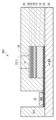
- FIG. 5 is a diagram showing the cross-sectional structure of the refractive index modulation region of the semiconductor optical modulation element of Example 1.
- the cross-sectional view of FIG. 5 shows a cross section perpendicular to the optical propagation direction of two interference optical waveguides 21a and 21b, cut along line V-V in FIG. 4.
- Interference optical waveguides 21a and 21b having the n-i-p-n type layer structure shown in FIG. 3(a) are formed on a semi-insulating InP substrate 20.
- FIG. 6 is a diagram showing the cross-sectional structure of the input optical waveguide of the semiconductor optical modulation element of Example 1.
- the cross-sectional view of FIG. 6 shows a cross section perpendicular to the optical propagation direction of the input optical waveguide 21-1 cut along the line VI-VI in FIG. 4.
- An input optical waveguide 21-1 having a structure obtained by partially modifying the n-i-p-n type layer structure shown in FIG. 3(a) is formed on an InP substrate 20. That is, in the n-i-p-n type layer structure shown in FIG. 3(a), the second n-type cladding layer 17 is replaced with semi-insulating InP or non-doped InP from the viewpoint of reducing optical loss.
- a DC bias electrode 22 is formed on the n-type contact layer 23 in contact with the first n-type cladding layer 12.
- the cross-sectional structure of the output optical waveguide 21-2 is also exactly the same as that of the input optical waveguide 21-1 in FIG. 6. Please note that Figures 5 and 6 are schematic diagrams, the thickness direction is greatly enlarged, and the relationship between the thicknesses of each layer is not accurately depicted.
- the optical modulation element 300 has the n-i-p-n type layer configuration of FIG. 3(a) on the n-type contact layer 23 formed on the InP substrate 20. From the InP substrate 20 upward, the first n-type cladding layer 12, the p-type electron barrier layer 13, the first buffer layer 14, the MQW layer 15 constituting the core, the second buffer layer 16, and the second n-type cladding layer 17 are arranged in this order.
- the n-type contact layer 23 is made of InGaAs with a carrier concentration of 5 ⁇ 10 18 /cm 3
- the first n-type cladding layer 12 and the second n-type cladding layer 17 are made of InP with a carrier concentration of 1 ⁇ 10 18 /cm 3.
- the p-type electron barrier layer 13 has a carrier concentration of 5 ⁇ 10 17 to 1 ⁇ 10 18 /cm 3 , taking into consideration the optical absorption coefficient and electrical resistivity, and InAlAs is used.
- InAlAs has a larger band gap than InP, exhibits p-type properties with the addition of carbon dopant, and can enhance the electron carrier blocking effect.
- the above-mentioned layers were sequentially grown and deposited on a semi-insulating InP (100) substrate by metal-organic vapor phase epitaxy (MOVPE).
- the band gap wavelength of the MQW layer 15, which is the core layer, is determined so that the electro-optic effect is highly efficient at the operating light wavelength, and light absorption is not an issue.
- the emission wavelength of the MQW layer 15 is set to about 1.4 ⁇ m.
- the MQW layer 15 is preferably formed with an InGaAlAs/InAlAs MQW structure.
- a multiple structure such as InGaAlAs/InGaAlAs may also be used.
- compositions of the n-type contact layers 23, 24 and the cladding layers are not limited to those described above, and for example, an InGaAsP composition may be used.
- the thickness of the first n-type cladding layer 12 is set to 120 nm or more, taking into account the overlap with the optical mode confined in the MQW layer.
- the second n-type cladding layer 17 above the area that does not contribute to modulation is removed by dry etching and wet etching to electrically isolate the elements.
- the areas where the second n-type cladding layer 17 was removed are backfilled with semi-insulating InP or non-doped InP 19 to reduce optical loss.
- an MZ interferometer optical waveguide pattern was formed from SiO2 formed in a direction equivalent to the [011] plane direction, and the ridge-shaped optical waveguide shown in Fig. 5 was formed using dry and wet etching processes.
- dry and wet etching was further performed to expose a part of the n-type contact layer 23 as shown in Fig. 6.
- BCB 25 benzocyclobutene (BCB) 25 was applied as an insulating film to flatten the unevenness of the optical waveguide, and after removing the BCB from the contact area, a capacitive-loaded traveling wave electrode pattern as shown in Figure 4 was formed by gold plating.
- the insulating film polyimide, which is an insulating low refractive index material, may be used instead of BCB.
- a predetermined bias was applied to the DC bias electrode 22 so that a reverse electric field was applied to the pn junction, and a high-frequency signal was fed to the signal electrode (coplanar strip line).
- a high-frequency signal was fed to the signal electrode (coplanar strip line).
- the present invention can reduce the wavelength dependency of the modulation output performance of an n-i-p-n type optical modulation element.
- This invention can be used in general optical communications.
Landscapes
- Physics & Mathematics (AREA)
- Nonlinear Science (AREA)
- General Physics & Mathematics (AREA)
- Optics & Photonics (AREA)
- Optical Modulation, Optical Deflection, Nonlinear Optics, Optical Demodulation, Optical Logic Elements (AREA)
Abstract
Est divulgué un élément de modulation optique InP qui a une hétérostructure de type n-i-p-n. Un élément de modulation optique selon la présente divulgation a une structure dans laquelle une couche d'InGaAsP est éliminée autant que possible d'une couche non dopée (i couche). Une première couche tampon (14) qui est positionnée entre une couche MQW (15) et une couche barrière aux électrons de type p (13) qui est adjacente à une première couche de gainage (12) a une configuration dans laquelle une composition contenant un matériau tel que l'InGaAsP qui provoque une absorption optique est éliminée. Pendant ce temps, une seconde couche tampon (16) qui est positionnée entre la couche MQW (15) et une seconde couche de gainage (17) peut contenir de l'InP ou de l'InGaAsP en tant que matériau constitutif. Cet élément de modulation optique améliore considérablement la dépendance à la longueur d'onde des performances d'un modulateur optique en raison d'un élément de modulation optique à semi-conducteur qui a une structure n-i-p-n de l'état de la technique.
Applications Claiming Priority (2)
| Application Number | Priority Date | Filing Date | Title |
|---|---|---|---|
| JP2023-092324 | 2023-06-05 | ||
| JP2023092324 | 2023-06-05 |
Publications (1)
| Publication Number | Publication Date |
|---|---|
| WO2024252989A1 true WO2024252989A1 (fr) | 2024-12-12 |
Family
ID=93795989
Family Applications (1)
| Application Number | Title | Priority Date | Filing Date |
|---|---|---|---|
| PCT/JP2024/019585 Ceased WO2024252989A1 (fr) | 2023-06-05 | 2024-05-28 | Élément de modulation optique à semi-conducteur |
Country Status (1)
| Country | Link |
|---|---|
| WO (1) | WO2024252989A1 (fr) |
Citations (7)
| Publication number | Priority date | Publication date | Assignee | Title |
|---|---|---|---|---|
| WO2009119145A1 (fr) * | 2008-03-28 | 2009-10-01 | 日本電気株式会社 | Modulateur optique à semi-conducteurs de type guide d'ondes et son procédé de fabrication |
| US20160109731A1 (en) * | 2013-06-09 | 2016-04-21 | Optonet, Inc. | Thin Layer Photonic Integrated Circuit Based Optical Signal Manipulators |
| WO2016194369A1 (fr) * | 2015-06-02 | 2016-12-08 | 日本電信電話株式会社 | Élément de modulation optique à semi-conducteurs |
| JP2017167359A (ja) * | 2016-03-16 | 2017-09-21 | 日本電信電話株式会社 | リッジ導波路型光変調器 |
| JP2018189780A (ja) * | 2017-05-01 | 2018-11-29 | 日本電信電話株式会社 | 化合物半導体系光変調素子 |
| WO2019211991A1 (fr) * | 2018-05-01 | 2019-11-07 | 日本電信電話株式会社 | Modulateur optique de mach-zehnder à semi-conducteur et modulateur optique iq l'utilisant |
| JP2023035532A (ja) * | 2021-09-01 | 2023-03-13 | 日本電信電話株式会社 | 半導体光変調素子 |
-
2024
- 2024-05-28 WO PCT/JP2024/019585 patent/WO2024252989A1/fr not_active Ceased
Patent Citations (7)
| Publication number | Priority date | Publication date | Assignee | Title |
|---|---|---|---|---|
| WO2009119145A1 (fr) * | 2008-03-28 | 2009-10-01 | 日本電気株式会社 | Modulateur optique à semi-conducteurs de type guide d'ondes et son procédé de fabrication |
| US20160109731A1 (en) * | 2013-06-09 | 2016-04-21 | Optonet, Inc. | Thin Layer Photonic Integrated Circuit Based Optical Signal Manipulators |
| WO2016194369A1 (fr) * | 2015-06-02 | 2016-12-08 | 日本電信電話株式会社 | Élément de modulation optique à semi-conducteurs |
| JP2017167359A (ja) * | 2016-03-16 | 2017-09-21 | 日本電信電話株式会社 | リッジ導波路型光変調器 |
| JP2018189780A (ja) * | 2017-05-01 | 2018-11-29 | 日本電信電話株式会社 | 化合物半導体系光変調素子 |
| WO2019211991A1 (fr) * | 2018-05-01 | 2019-11-07 | 日本電信電話株式会社 | Modulateur optique de mach-zehnder à semi-conducteur et modulateur optique iq l'utilisant |
| JP2023035532A (ja) * | 2021-09-01 | 2023-03-13 | 日本電信電話株式会社 | 半導体光変調素子 |
Similar Documents
| Publication | Publication Date | Title |
|---|---|---|
| JP2809124B2 (ja) | 光半導体集積素子およびその製造方法 | |
| JP6458143B2 (ja) | 半導体光変調素子 | |
| CN101529313B (zh) | 半导体光调制器 | |
| EP2230549B1 (fr) | Modulateur de lumière à semi-conducteur et dispositif de modulation de lumière | |
| JP5170236B2 (ja) | 導波路型半導体光変調器及びその製造方法 | |
| JP2606079B2 (ja) | 光半導体素子 | |
| US7142342B2 (en) | Electroabsorption modulator | |
| JP3809941B2 (ja) | 電界吸収型光変調器 | |
| JP5801589B2 (ja) | 光変調素子 | |
| JP2018189780A (ja) | 化合物半導体系光変調素子 | |
| JP2005116644A (ja) | 半導体光電子導波路 | |
| JP7569294B2 (ja) | 半導体光変調素子 | |
| JPH01319986A (ja) | 半導体レーザ装置 | |
| WO2024252989A1 (fr) | Élément de modulation optique à semi-conducteur | |
| EP3506001B1 (fr) | Modulateur optique | |
| US8735868B2 (en) | Semiconductor optical modulator | |
| JP6006611B2 (ja) | 半導体光変調素子 | |
| JP6491612B2 (ja) | 半導体光集積素子 | |
| JP4283079B2 (ja) | 半導体光電子導波路 | |
| CN121642745A (zh) | 半导体激光器及光模块 | |
| KR100275488B1 (ko) | 다중 양자우물 구조의 수동 광도파로가 집적된 초고속 광변조기및 그 제조 방법과 그를 이용한 광변조 방법 | |
| JP2007157884A (ja) | 光変調器集積光源 | |
| Xu et al. | Efficient deeply etched InP/InGaAsP phase shifters with low dark current | |
| JP2007304472A (ja) | 半導体光変調器 | |
| JPH09121075A (ja) | 半導体レーザ装置 |
Legal Events
| Date | Code | Title | Description |
|---|---|---|---|
| 121 | Ep: the epo has been informed by wipo that ep was designated in this application |
Ref document number: 24819220 Country of ref document: EP Kind code of ref document: A1 |
|
| ENP | Entry into the national phase |
Ref document number: 2025526065 Country of ref document: JP Kind code of ref document: A |
|
| WWE | Wipo information: entry into national phase |
Ref document number: 2025526065 Country of ref document: JP |
|
| NENP | Non-entry into the national phase |
Ref country code: DE |