WO2024257211A1 - 積層セラミックコンデンサ - Google Patents
積層セラミックコンデンサ Download PDFInfo
- Publication number
- WO2024257211A1 WO2024257211A1 PCT/JP2023/021882 JP2023021882W WO2024257211A1 WO 2024257211 A1 WO2024257211 A1 WO 2024257211A1 JP 2023021882 W JP2023021882 W JP 2023021882W WO 2024257211 A1 WO2024257211 A1 WO 2024257211A1
- Authority
- WO
- WIPO (PCT)
- Prior art keywords
- coverage
- layer
- intermediate region
- region
- opposing
- Prior art date
- Legal status (The legal status is an assumption and is not a legal conclusion. Google has not performed a legal analysis and makes no representation as to the accuracy of the status listed.)
- Ceased
Links
Images


Classifications
-
- H—ELECTRICITY
- H01—ELECTRIC ELEMENTS
- H01G—CAPACITORS; CAPACITORS, RECTIFIERS, DETECTORS, SWITCHING DEVICES, LIGHT-SENSITIVE OR TEMPERATURE-SENSITIVE DEVICES OF THE ELECTROLYTIC TYPE
- H01G4/00—Fixed capacitors; Processes of their manufacture
- H01G4/002—Details
- H01G4/005—Electrodes
- H01G4/012—Form of non-self-supporting electrodes
-
- H—ELECTRICITY
- H01—ELECTRIC ELEMENTS
- H01G—CAPACITORS; CAPACITORS, RECTIFIERS, DETECTORS, SWITCHING DEVICES, LIGHT-SENSITIVE OR TEMPERATURE-SENSITIVE DEVICES OF THE ELECTROLYTIC TYPE
- H01G4/00—Fixed capacitors; Processes of their manufacture
- H01G4/002—Details
- H01G4/005—Electrodes
- H01G4/008—Selection of materials
- H01G4/0085—Fried electrodes
-
- H—ELECTRICITY
- H01—ELECTRIC ELEMENTS
- H01G—CAPACITORS; CAPACITORS, RECTIFIERS, DETECTORS, SWITCHING DEVICES, LIGHT-SENSITIVE OR TEMPERATURE-SENSITIVE DEVICES OF THE ELECTROLYTIC TYPE
- H01G4/00—Fixed capacitors; Processes of their manufacture
- H01G4/002—Details
- H01G4/018—Dielectrics
- H01G4/06—Solid dielectrics
- H01G4/08—Inorganic dielectrics
- H01G4/12—Ceramic dielectrics
-
- H—ELECTRICITY
- H01—ELECTRIC ELEMENTS
- H01G—CAPACITORS; CAPACITORS, RECTIFIERS, DETECTORS, SWITCHING DEVICES, LIGHT-SENSITIVE OR TEMPERATURE-SENSITIVE DEVICES OF THE ELECTROLYTIC TYPE
- H01G4/00—Fixed capacitors; Processes of their manufacture
- H01G4/002—Details
- H01G4/228—Terminals
- H01G4/232—Terminals electrically connecting two or more layers of a stacked or rolled capacitor
-
- H—ELECTRICITY
- H01—ELECTRIC ELEMENTS
- H01G—CAPACITORS; CAPACITORS, RECTIFIERS, DETECTORS, SWITCHING DEVICES, LIGHT-SENSITIVE OR TEMPERATURE-SENSITIVE DEVICES OF THE ELECTROLYTIC TYPE
- H01G4/00—Fixed capacitors; Processes of their manufacture
- H01G4/30—Stacked capacitors
-
- H—ELECTRICITY
- H01—ELECTRIC ELEMENTS
- H01G—CAPACITORS; CAPACITORS, RECTIFIERS, DETECTORS, SWITCHING DEVICES, LIGHT-SENSITIVE OR TEMPERATURE-SENSITIVE DEVICES OF THE ELECTROLYTIC TYPE
- H01G4/00—Fixed capacitors; Processes of their manufacture
- H01G4/002—Details
- H01G4/018—Dielectrics
- H01G4/06—Solid dielectrics
- H01G4/08—Inorganic dielectrics
- H01G4/12—Ceramic dielectrics
- H01G4/1209—Ceramic dielectrics characterised by the ceramic dielectric material
- H01G4/1218—Ceramic dielectrics characterised by the ceramic dielectric material based on titanium oxides or titanates
- H01G4/1227—Ceramic dielectrics characterised by the ceramic dielectric material based on titanium oxides or titanates based on alkaline earth titanates
-
- H—ELECTRICITY
- H01—ELECTRIC ELEMENTS
- H01G—CAPACITORS; CAPACITORS, RECTIFIERS, DETECTORS, SWITCHING DEVICES, LIGHT-SENSITIVE OR TEMPERATURE-SENSITIVE DEVICES OF THE ELECTROLYTIC TYPE
- H01G4/00—Fixed capacitors; Processes of their manufacture
- H01G4/002—Details
- H01G4/018—Dielectrics
- H01G4/06—Solid dielectrics
- H01G4/08—Inorganic dielectrics
- H01G4/12—Ceramic dielectrics
- H01G4/1209—Ceramic dielectrics characterised by the ceramic dielectric material
- H01G4/1236—Ceramic dielectrics characterised by the ceramic dielectric material based on zirconium oxides or zirconates
-
- H—ELECTRICITY
- H01—ELECTRIC ELEMENTS
- H01G—CAPACITORS; CAPACITORS, RECTIFIERS, DETECTORS, SWITCHING DEVICES, LIGHT-SENSITIVE OR TEMPERATURE-SENSITIVE DEVICES OF THE ELECTROLYTIC TYPE
- H01G4/00—Fixed capacitors; Processes of their manufacture
- H01G4/002—Details
- H01G4/228—Terminals
- H01G4/232—Terminals electrically connecting two or more layers of a stacked or rolled capacitor
- H01G4/2325—Terminals electrically connecting two or more layers of a stacked or rolled capacitor characterised by the material of the terminals
Definitions
- the present invention relates to a multilayer ceramic capacitor.
- Multilayer ceramic capacitors are known in the art. Generally, multilayer ceramic capacitors have a laminate in which dielectric layers and internal electrode layers are alternately stacked (see Patent Document 1). There is a demand for such multilayer ceramic capacitors to be further miniaturized, have higher capacitance, and have improved reliability. For this reason, ferroelectric materials with high dielectric constants are sometimes used as materials for the dielectric layers. There have also been attempts to make the dielectric layers thinner, make the internal electrode layers thinner, and increase the number of stacked layers for these layers.
- Such dielectric layers have piezoelectricity and electrostriction. Therefore, when a voltage is applied to a multilayer ceramic capacitor having such a dielectric layer, a strain corresponding to the magnitude of the applied voltage is generated in the laminate due to the electrostrictive effect, and stress is generated inside the multilayer ceramic capacitor.
- the objective of the present invention is to provide a multilayer ceramic capacitor that can ensure capacitance density, maintain connectivity between the internal electrode layers and the external electrodes, and reduce stress concentration caused by the electrostrictive effect when voltage is applied.
- the multilayer ceramic capacitor according to the present invention is a multilayer ceramic capacitor comprising a laminate including a plurality of laminated dielectric layers and a plurality of laminated internal electrode layers, the laminate including a first main surface and a second main surface facing each other in the lamination direction, a first side surface and a second side surface facing each other in a width direction perpendicular to the lamination direction, and a first end surface and a second end surface facing each other in a length direction perpendicular to the lamination direction and the width direction, a first external electrode arranged on the first end surface side, and a second external electrode arranged on the second end surface side, the plurality of internal electrode layers including a first internal electrode layer and a second internal electrode layer, the first internal electrode layer having a first extension portion having one end thereof drawn out to the first end surface and connected to the first external electrode, and a first opposing portion connected to the first extension portion and facing the second internal electrode layer arranged adjacent to the first internal electrode layer in the lamination direction, and the second internal electrode layer having
- the first lead portion having a first external electrode side region adjacent to the connection portion with the first opposing portion, a first opposing portion side region adjacent to the connection portion with the first opposing portion, and a first intermediate region between the first external electrode side region and the first opposing portion side region
- the second lead portion has a first external electrode side region adjacent to the connection portion with the second external electrode
- the first and second intermediate regions have a first external electrode side region, a second opposing portion side region near the connection with the second opposing portion, and a second intermediate region between the second external electrode side region and the second opposing portion side region, and the coverage of the first intermediate region and the second intermediate region is lower than the coverage of the first external electrode side region and the second external electrode side region, and the coverage of the first intermediate region and the second intermediate region is lower than the coverage of the first opposing portion and the second opposing portion.
- the present invention provides a multilayer ceramic capacitor that can ensure capacitance density, maintain connectivity between the internal electrode layers and the external electrodes, and reduce stress concentration caused by the electrostrictive effect when voltage is applied.
- FIG. 1 is an external perspective view of a multilayer ceramic capacitor in accordance with a first embodiment; This is a cross-sectional view of FIG. 1 taken along line II-II.
- FIG. 3 is a cross-sectional view taken along line III-III of FIG. 2.
- FIG. 3 is a cross-sectional view of FIG. 2 along the line IVA-IVA.
- 4 is a cross-sectional view taken along line IVB-IVB of FIG. 2.
- FIG. 3 is an enlarged cross-sectional view showing a schematic view of a portion indicated by R1 in FIG. 2 .
- FIG. 3 is an enlarged cross-sectional view showing a schematic view of a portion indicated by R2 in FIG. 2 .
- FIG. 3 is an enlarged cross-sectional view showing a schematic view of a portion indicated by R1 in FIG. 2 in the multilayer ceramic capacitor in accordance with a second embodiment.
- 4 is an enlarged cross-sectional view showing a schematic view of a portion indicated by R2 in FIG. 2 in the multilayer ceramic capacitor in accordance with a second embodiment.
- Fig. 1 is an external perspective view of the multilayer ceramic capacitor 1 according to the embodiment.
- Fig. 2 is a cross-sectional view taken along II-II in Fig. 1.
- Fig. 3 is a cross-sectional view taken along III-III in Fig. 2.
- Fig. 4A is a cross-sectional view taken along IVA-IVA in Fig. 2.
- Fig. 4B is a cross-sectional view taken along IVB-IVB in Fig. 2.
- the multilayer ceramic capacitor 1 has a substantially rectangular parallelepiped shape.
- the multilayer ceramic capacitor 1 includes a laminate 10 having a substantially rectangular parallelepiped shape, and a pair of external electrodes 40 arranged at a distance from each other on both ends of the laminate 10.
- arrow T indicates the stacking direction of the multilayer ceramic capacitor 1 and the laminate 10. This stacking direction T is also the thickness direction and height direction of the multilayer ceramic capacitor 1 and the laminate 10.
- arrow L indicates the length direction of the multilayer ceramic capacitor 1 and the laminate 10, which is perpendicular to the stacking direction T.
- arrow W indicates the width direction of the multilayer ceramic capacitor 1 and the laminate 10, which is perpendicular to the stacking direction T and the length direction L.
- a pair of external electrodes 40 are respectively disposed at one end and the other end of the length direction L of the laminate 10.
- FIGS. 1 to 4B show an XYZ orthogonal coordinate system.
- the length direction L of the multilayer ceramic capacitor 1 and the laminate 10 corresponds to the X direction.
- the width direction W of the multilayer ceramic capacitor 1 and the laminate 10 corresponds to the Y direction.
- the stacking direction T of the multilayer ceramic capacitor 1 and the laminate 10 corresponds to the Z direction.
- the cross section shown in FIG. 2 is also called the LT cross section.
- the cross section shown in FIG. 3 is also called the WT cross section.
- the cross sections shown in FIG. 4A and FIG. 4B are also called the LW cross section.
- the laminate 10 includes a first main surface TS1 and a second main surface TS2 that face the stacking direction T, a first end surface LS1 and a second end surface LS2 that face the length direction L that is perpendicular to the stacking direction T, and a first side surface WS1 and a second side surface WS2 that face the width direction W that is perpendicular to the stacking direction T and the length direction L.
- the laminate 10 has a generally rectangular parallelepiped shape.
- the dimension of the laminate 10 in the length direction L is not necessarily longer than the dimension in the width direction W. It is preferable that the corners and ridges of the laminate 10 are rounded. A corner is a portion where three faces of the laminate intersect, and a ridge is a portion where two faces of the laminate intersect. Incidentally, unevenness may be formed on part or all of the surfaces constituting the laminate 10.
- the dimensions of the laminate 10 are not particularly limited, but if the dimension of the laminate 10 in the length direction L is the L dimension, it is preferable that the L dimension is 0.2 mm or more and 6 mm or less. If the dimension of the laminate 10 in the stacking direction T is the T dimension, it is preferable that the T dimension is 0.05 mm or more and 5 mm or less. If the dimension of the laminate 10 in the width direction W is the W dimension, it is preferable that the W dimension is 0.1 mm or more and 5 mm or less.
- the laminate 10 has an inner layer portion 11, and a first main surface side outer layer portion 12 and a second main surface side outer layer portion 13 arranged to sandwich the inner layer portion 11 in the stacking direction T.
- the inner layer portion 11 includes a plurality of dielectric layers 20 and a plurality of internal electrode layers 30 that are alternately stacked in the stacking direction T.
- the inner layer portion 11 includes the internal electrode layer 30 located closest to the first principal surface TS1 to the internal electrode layer 30 located closest to the second principal surface TS2 in the stacking direction T.
- the multiple internal electrode layers 30 are arranged opposite each other with the dielectric layer 20 interposed therebetween.
- the inner layer portion 11 is a portion that generates electrostatic capacitance and essentially functions as a capacitor.
- the multiple dielectric layers 20 are made of a dielectric material.
- the dielectric material may be, for example, a dielectric ceramic containing components such as BaTiO3 , CaTiO3 , SrTiO3 , or CaZrO3 .
- the dielectric material may also be a material in which a subcomponent such as a Mn compound, an Fe compound, a Cr compound, a Co compound, or a Ni compound is added to the main components. It is particularly preferable that the dielectric material is a material containing BaTiO3 as the main component.
- the thickness of the dielectric layer 20 is preferably 0.2 ⁇ m or more and 10 ⁇ m or less.
- the number of dielectric layers 20 to be stacked is preferably 15 or more and 1200 or less.
- the number of dielectric layers 20 is the total number of the dielectric layers 20 in the inner layer portion 11 and the number of dielectric layers 20 in each of the first main surface side outer layer portion 12 and the second main surface side outer layer portion 13.
- the multiple internal electrode layers 30 include multiple first internal electrode layers 31 and multiple second internal electrode layers 32.
- the first internal electrode layers 31 and the second internal electrode layers 32 are alternately arranged in the stacking direction T with the dielectric layer 20 sandwiched therebetween.
- the first internal electrode layer 31 is extended to the first end face LS1.
- the second internal electrode layer 32 is extended to the second end face LS2.
- the first internal electrode layer 31 and the second internal electrode layer 32 may be collectively referred to as the internal electrode layer 30.
- the first internal electrode layer 31 has a first opposing portion 31A and a first extension portion 31B.
- the first opposing portion 31A is a region that faces the second internal electrode layer 32 with the dielectric layer 20 sandwiched therebetween, and is located inside the laminate 10.
- the first extension portion 31B is a portion that is extended from the first opposing portion 31A to the first end face LS1, and is exposed at the first end face LS1.
- the second internal electrode layer 32 has a second opposing portion 32A and a second extension portion 32B.
- the second opposing portion 32A is a region that faces the first internal electrode layer 31 with the dielectric layer 20 sandwiched therebetween, and is located inside the laminate 10.
- the second extension portion 32B is a portion that is extended from the second opposing portion 32A to the second end face LS2, and is exposed at the second end face LS2.
- the first opposing portion 31A and the second opposing portion 32A face each other via the dielectric layer 20, forming a capacitance and exhibiting the characteristics of a capacitor.
- the shapes of the first opposing portion 31A and the second opposing portion 32A are not particularly limited, but are preferably rectangular. However, the corners of the rectangular shape may be rounded or the corners of the rectangular shape may be formed at an angle.
- the shapes of the first pull-out portion 31B and the second pull-out portion 32B are not particularly limited, but are preferably rectangular. However, the corners of the rectangular shape may be rounded or the corners of the rectangular shape may be formed at an angle.
- the dimension in the width direction W of the first opposing portion 31A and the dimension in the width direction W of the first pull-out portion 31B may be the same, or one of the dimensions may be smaller.
- the dimension in the width direction W of the second opposing portion 32A and the dimension in the width direction W of the second pull-out portion 32B may be the same, or one of the dimensions may be smaller.
- the first internal electrode layer 31 and the second internal electrode layer 32 are made of an appropriate conductive material, such as a metal such as Ni, Cu, Ag, Pd, or Au, or an alloy containing at least one of these metals. When an alloy is used, the first internal electrode layer 31 and the second internal electrode layer 32 may be made of, for example, an Ag-Pd alloy.
- each of the first internal electrode layer 31 and the second internal electrode layer 32 is preferably, for example, 0.2 ⁇ m or more and 2.0 ⁇ m or less4.
- the total number of the first internal electrode layers 31 and the second internal electrode layers 32 is preferably 15 or more and 1000 or less.
- the first main surface side outer layer portion 12 is located on the first main surface TS1 side of the laminate 10.
- the first main surface side outer layer portion 12 is a collection of multiple dielectric layers 20 located between the first main surface TS1 and the internal electrode layer 30 closest to the first main surface TS1.
- the second main surface side outer layer portion 13 is located on the second main surface TS2 side of the laminate 10.
- the second main surface side outer layer portion 13 is a collection of multiple dielectric layers 20 located between the second main surface TS2 and the internal electrode layer 30 closest to the second main surface TS2.
- the dielectric layers 20 used in the first main surface side outer layer portion 12 and the second main surface side outer layer portion 13 may be the same as the dielectric layers 20 used in the internal layer portion 11.
- the laminate 10 has an opposing electrode portion 11E.
- the opposing electrode portion 11E is a portion where the first opposing portion 31A of the first internal electrode layer 31 and the second opposing portion 32A of the second internal electrode layer 32 face each other.
- the opposing electrode portion 11E is configured as a part of the inner layer portion 11.
- Figures 4A and 4B show the range of the width direction W and length direction L of the opposing electrode portion 11E.
- the opposing electrode portion 11E is also called the effective portion of the capacitor.
- the laminate 10 has a side surface outer layer portion.
- the side surface outer layer portion has a first side surface outer layer portion WG1 and a second side surface outer layer portion WG2.
- the first side surface outer layer portion WG1 is a portion including the dielectric layer 20 located between the opposing electrode portion 11E and the first side surface WS1.
- the second side surface outer layer portion WG2 is a portion including the dielectric layer 20 located between the opposing electrode portion 11E and the second side surface WS2.
- Figures 3, 4A, and 4B show the range of the width direction W of the first side surface outer layer portion WG1 and the second side surface outer layer portion WG2.
- the side surface outer layer portion is also called a W gap or a side gap.
- the laminate 10 has an end surface side outer layer portion.
- the end surface side outer layer portion has a first end surface side outer layer portion LG1 and a second end surface side outer layer portion LG2.
- the first end surface side outer layer portion LG1 is a portion that includes the dielectric layer 20 and the first lead portion 31B, located between the counter electrode portion 11E and the first end surface LS1.
- the first end surface side outer layer portion LG1 is an assembly of the portions of the multiple dielectric layers 20 on the first end surface LS1 side and the multiple first lead portions 31B.
- the second end surface side outer layer portion LG2 is a portion that includes the dielectric layer 20 and the second lead portion 32B, located between the counter electrode portion 11E and the second end surface LS2.
- the second end surface side outer layer portion LG2 is an assembly of the portions of the multiple dielectric layers 20 on the second end surface LS2 side and the multiple second lead portions 32B. 2, 4A, and 4B show the range of the length direction L of the first end surface side outer layer portion LG1 and the second end surface side outer layer portion LG2.
- the end surface side outer layer portion is also called the L gap or end gap.
- the external electrode 40 has a first external electrode 40A arranged on the first end face LS1 side of the laminate 10, and a second external electrode 40B arranged on the second end face LS2 side of the laminate 10.
- the first external electrode 40A and the second external electrode 40B have the same basic configuration. Furthermore, the first external electrode 40A and the second external electrode 40B have shapes that are roughly plane-symmetrical with respect to a WT cross section at the center of the longitudinal direction L of the multilayer ceramic capacitor 1. Therefore, in the following, when it is not necessary to distinguish between the first external electrode 40A and the second external electrode 40B, the first external electrode 40A and the second external electrode 40B may be collectively referred to as the external electrodes 40.
- the first external electrode 40A is disposed on the first end face LS1.
- the first external electrode 40A is in contact with the first lead portions 31B of the first internal electrode layers 31 exposed on the first end face LS1. This allows the first external electrode 40A to be electrically connected to the first internal electrode layers 31.
- the first external electrode 40A may also be disposed on a portion of the first main surface TS1 and a portion of the second main surface TS2, as well as a portion of the first side surface WS1 and a portion of the second side surface WS2.
- the first external electrode 40A is formed to extend from the first end face LS1 to a portion of the first main surface TS1 and a portion of the second main surface TS2, as well as a portion of the first side surface WS1 and a portion of the second side surface WS2.
- the second external electrode 40B is disposed on the second end face LS2.
- the second external electrode 40B is in contact with the second lead portions 32B of the second internal electrode layers 32 exposed on the second end face LS2. This allows the second external electrode 40B to be electrically connected to the second internal electrode layers 32.
- the second external electrode 40B may also be disposed on a portion of the first main surface TS1 and a portion of the second main surface TS2, as well as a portion of the first side surface WS1 and a portion of the second side surface WS2.
- the second external electrode 40B is formed to extend from the second end face LS2 to a portion of the first main surface TS1 and a portion of the second main surface TS2, as well as a portion of the first side surface WS1 and a portion of the second side surface WS2.
- the first opposing portion 31A of the first internal electrode layer 31 and the second opposing portion 32A of the second internal electrode layer 32 face each other via the dielectric layer 20, forming a capacitance. Therefore, the characteristics of a capacitor are manifested between the first external electrode 40A to which the first internal electrode layer 31 is connected and the second external electrode 40B to which the second internal electrode layer 32 is connected.
- the first external electrode 40A has a first base electrode layer 50A and a first plating layer 60A disposed on the first base electrode layer 50A.
- the second external electrode 40B has a second base electrode layer 50B and a second plating layer 60B disposed on the second base electrode layer 50B.
- the first base electrode layer 50A is disposed on the first end face LS1.
- the first base electrode layer 50A is connected to the first lead portions 31B of each of the first internal electrode layers 31 exposed at the first end face LS1.
- the first base electrode layer 50A is formed to extend from the first end face LS1 to a portion of the first main surface TS1 and a portion of the second main surface TS2, as well as a portion of the first side surface WS1 and a portion of the second side surface WS2.
- the second base electrode layer 50B is disposed on the second end face LS2.
- the second base electrode layer 50B is in contact with the second lead portions 32B of each of the multiple second internal electrode layers 32 exposed at the second end face LS2.
- the second base electrode layer 50B is formed to extend from the second end face LS2 to a portion of the first main surface TS1 and a portion of the second main surface TS2, as well as a portion of the first side surface WS1 and a portion of the second side surface WS2.
- the first base electrode layer 50A and the second base electrode layer 50B of this embodiment are baked layers.
- the baked layer preferably contains a metal component and either a glass component or a ceramic component, or both.
- the metal component includes at least one selected from, for example, Cu, Ni, Ag, Pd, Ag-Pd alloy, Au, etc.
- the glass component includes at least one selected from, for example, B, Si, Ba, Mg, Al, Li, etc.
- the ceramic component may be the same type of ceramic material as the dielectric layer 20, or a different type of ceramic material.
- the ceramic component includes at least one selected from, for example, BaTiO 3 , CaTiO 3 , (Ba, Ca)TiO 3 , SrTiO 3 , CaZrO 3, etc.
- the baked layer is formed by, for example, applying a conductive paste containing glass and metal to the laminate 10 and baking it.
- the baked layer can be formed by simultaneously baking the laminate chip before firing, which is the material of the laminate 10 having a plurality of internal electrodes and dielectric layers, and the conductive paste applied to the laminate chip.
- the baked layer may be formed by baking the laminate 10 after the laminate chip is fired to obtain the laminate 10 and then applying the conductive paste to the laminate 10 and baking it.
- it is preferable to form the baked layer by adding a ceramic material instead of the glass component and baking it. In that case, it is particularly preferable to use the same type of ceramic material as the dielectric layer 20 as the ceramic material to be added.
- the baked layer may be multiple layers.
- the thickness of the first base electrode layer 50A located on the first end surface LS1 in the length direction L is preferably, for example, about 3 ⁇ m or more and 200 ⁇ m or less at the center of the stacking direction T and width direction W of the first base electrode layer 50A.
- the thickness of the second base electrode layer 50B located on the second end surface LS2 in the length direction L is preferably, for example, about 3 ⁇ m or more and 200 ⁇ m or less at the center of the stacking direction T and width direction W of the second base electrode layer 50B.
- the thickness of the first base electrode layer 50A provided on this portion is preferably, for example, about 3 ⁇ m or more and 40 ⁇ m or less at the center of the length direction L and width direction W of the first base electrode layer 50A provided on this portion.
- the thickness of the first base electrode layer 50A provided on this portion in the width direction W is preferably, for example, about 3 ⁇ m or more and 40 ⁇ m or less at the center of the length direction L and stacking direction T of the first base electrode layer 50A provided on this portion.
- the thickness of the second base electrode layer 50B provided on this portion is preferably, for example, about 3 ⁇ m or more and 40 ⁇ m or less at the center in the length direction L and width direction W of the second base electrode layer 50B provided on this portion.
- the thickness of the second base electrode layer 50B provided on this portion in the width direction W is preferably, for example, about 3 ⁇ m or more and 40 ⁇ m or less at the center of the length direction L and stacking direction T of the second base electrode layer 50B provided on this portion.
- the first and second base electrode layers 50A and 50B are not limited to baked layers.
- the first and second base electrode layers 50A and 50B include at least one selected from a baked layer, a conductive resin layer, a thin film layer, and the like.
- the first and second base electrode layers 50A and 50B may be thin film layers.
- the thin film layers are formed by a thin film formation method such as a sputtering method or a vapor deposition method.
- the thin film layer is a layer of 10 ⁇ m or less on which metal particles are deposited.
- the first plating layer 60A is arranged to cover the first base electrode layer 50A.
- the second plating layer 60B is arranged to cover the second base electrode layer 50B.
- the first plating layer 60A and the second plating layer 60B may contain, for example, at least one selected from Cu, Ni, Sn, Ag, Pd, an Ag-Pd alloy, Au, etc.
- the first plating layer 60A and the second plating layer 60B may each be formed of multiple layers.
- the first plating layer 60A and the second plating layer 60B preferably have a two-layer structure in which a Sn plating layer is formed on a Ni plating layer.
- the first plating layer 60A is disposed so as to cover the first base electrode layer 50A.
- the first plating layer 60A has a first Ni plating layer 61A and a first Sn plating layer 62A located on the first Ni plating layer 61A.
- the second plating layer 60B is disposed so as to cover the second base electrode layer 50B.
- the second plating layer 60B has a second Ni plating layer 61B and a second Sn plating layer 62B located on the second Ni plating layer 61B.
- the Ni plating layer prevents the first and second underlying electrode layers 50A and 50B from being eroded by solder when mounting the multilayer ceramic capacitor 1.
- the Sn plating layer improves the wettability of the solder when mounting the multilayer ceramic capacitor 1, thereby making it easier to mount the multilayer ceramic capacitor 1.
- the thickness of each of the first Ni plating layer 61A, the first Sn plating layer 62A, the second Ni plating layer 61B, and the second Sn plating layer 62B is preferably 2 ⁇ m or more and 10 ⁇ m or less.
- the external electrode 40 of this embodiment may have, for example, a conductive resin layer containing conductive particles and a thermosetting resin.
- the conductive resin layer may be arranged so as to cover the baked layer.
- the conductive resin layer is arranged between the baked layer and the plating layer (first plating layer 60A, second plating layer 60B).
- the conductive resin layer may completely cover the baked layer, or may cover a portion of the baked layer.
- the conductive resin layer containing a thermosetting resin is more flexible than a conductive layer made of, for example, a plating film or a fired conductive paste. Therefore, even if the multilayer ceramic capacitor 1 is subjected to a physical shock or a shock caused by a thermal cycle, the conductive resin layer functions as a buffer layer. Therefore, the conductive resin layer suppresses the occurrence of cracks in the multilayer ceramic capacitor 1.
- the metal constituting the conductive particles may be Ag, Cu, Ni, Sn, Bi, or an alloy containing these.
- the conductive particles preferably contain Ag.
- the conductive particles are, for example, Ag metal powder. Ag has the lowest resistivity of all metals, making it suitable as an electrode material. In addition, Ag is a precious metal, so it is resistant to oxidation and has high weather resistance. Therefore, Ag metal powder is suitable as a conductive particle.
- the conductive particles may also be metal powder with an Ag-coated surface.
- the metal powder is preferably a powder of Cu, Ni, Sn, Bi or an alloy thereof. In order to make the base metal less expensive while maintaining the properties of Ag, it is preferable to use Ag-coated metal powder.
- the conductive particles may be Cu or Ni that has been subjected to an anti-oxidation treatment.
- the conductive particles may also be metal powder with a surface coating of Sn, Ni, or Cu.
- the metal powder is Ag, Cu, Ni, Sn, Bi, or an alloy powder of these.
- the shape of the conductive particles is not particularly limited.
- the conductive particles may be spherical, flat, or other shapes, but it is preferable to use a mixture of spherical metal powder and flat metal powder.
- the conductive particles contained in the conductive resin layer are primarily responsible for ensuring the electrical conductivity of the conductive resin layer. Specifically, when multiple conductive particles come into contact with each other, a conductive path is formed inside the conductive resin layer.
- the resin constituting the conductive resin layer may contain at least one selected from various known thermosetting resins, such as epoxy resin, phenolic resin, urethane resin, silicone resin, and polyimide resin.
- thermosetting resins such as epoxy resin, phenolic resin, urethane resin, silicone resin, and polyimide resin.
- epoxy resin which has excellent heat resistance, moisture resistance, and adhesion, is one of the most suitable resins.
- the resin of the conductive resin layer contains a hardener in addition to the thermosetting resin.
- the hardener of the epoxy resin may be various known compounds such as phenol-based, amine-based, acid anhydride-based, imidazole-based, active ester-based, and amide-imide-based compounds.
- the conductive resin layer may be formed of multiple layers.
- the thickness of the thickest part of the conductive resin layer is preferably 10 ⁇ m or more and 150 ⁇ m or less.
- the multilayer ceramic capacitor 1 may have a configuration including plating layers that are directly and electrically connected to the first internal electrode layer 31 and the second internal electrode layer 32.
- the plating layers may be formed after a catalyst is disposed on the surface of the laminate 10 as a pretreatment.
- the plating layer is preferably a multi-layer structure.
- the lower plating layer and the upper plating layer each preferably contain at least one metal selected from, for example, Cu, Ni, Sn, Pb, Au, Ag, Pd, Bi, or Zn, or an alloy containing these metals.
- the lower plating layer is more preferably formed using Ni, which has solder barrier properties.
- the upper plating layer is more preferably formed using Sn or Au, which has good solder wettability.
- the lower plating layer is preferably formed using Cu, which has good bonding properties with Ni.
- the upper plating layer may be formed as necessary, and the external electrode 40 may be composed of only the lower plating layer.
- the upper plating layer may be the outermost layer, or another plating layer may be formed on the surface of the upper plating layer.
- each plating layer that is placed without providing an underlying electrode layer is preferably 2 ⁇ m or more and 10 ⁇ m or less. It is preferable that the plating layer does not contain glass.
- the metal ratio per unit volume of the plating layer is preferably 99 volume % or more.
- the thickness of the base electrode layer can be reduced. Therefore, the dimension of the multilayer ceramic capacitor 1 in the height direction T can be reduced by the amount of the reduction in the thickness of the base electrode layer, thereby making it possible to reduce the height of the multilayer ceramic capacitor 1.
- the thickness of the dielectric layer 20 sandwiched between the first internal electrode layer 31 and the second internal electrode layer 32 can be increased by the amount of the reduction in the thickness of the base electrode layer, thereby improving the thickness of the element. In this way, by forming the plating layer directly on the laminate 10, the design freedom of the multilayer ceramic capacitor can be improved.
- the above is the basic configuration of the multilayer ceramic capacitor 1 according to the embodiment. If the lengthwise dimension of the multilayer ceramic capacitor 1 including the laminate 10 and the external electrodes 40 is taken as L dimension, then it is preferable that L dimension is 0.2 mm or more and 6 mm or less. If the dimension of the multilayer ceramic capacitor 1 in the stacking direction is taken as T dimension, then it is preferable that T dimension is 0.05 mm or more and 5 mm or less. If the widthwise dimension of the multilayer ceramic capacitor 1 is taken as W dimension, then it is preferable that W dimension is 0.1 mm or more and 5 mm or less.
- the inventors of the present application have found, through repeated studies, experiments, and simulations, that it is desirable to make the coverage of the internal electrode layers appropriate in order to improve the overall quality of the multilayer ceramic capacitor. This point will be explained below.
- multilayer ceramic capacitors the establishment of technology to increase the coverage of the internal electrode layers in order to improve the capacitance density is underway. The coverage is also referred to as the coverage rate of the internal electrode layers relative to the dielectric layer.
- improving the coverage also contributes to improving the connectivity between the internal electrode layers and the external electrodes.
- FIG. 5A is an enlarged cross-sectional view showing a schematic view of the portion indicated by R1 in FIG. 2.
- FIG. 5B is an enlarged cross-sectional view showing a schematic view of the portion indicated by R2 in FIG. 2.
- FIGS. 5A and 5B are portions of an LT cross-section. In FIGS. 5A and 5B, the dielectric layer 20, the first internal electrode layer 31, and the second internal electrode layer 32 in the laminate 10, the first external electrode 40A, and the second external electrode 40B are shown.
- the first internal electrode layer 31 has a first extension portion 31B, one end of which is extended to the first end surface LS1 and connected to the first external electrode 40A, and a first opposing portion 31A, which is connected to the first extension portion 31B and faces the second internal electrode layer 32 arranged adjacent to it in the stacking direction T.
- the second internal electrode layer 32 has a second lead-out portion 32B, one end of which is led out to the second end face LS2 and connected to the second external electrode 40B, and a second opposing portion 32A, which is connected to the second lead-out portion 32B and faces the first internal electrode layer 31 arranged adjacent to it in the stacking direction T.
- the first lead-out portion 31B has a first external electrode side region 31BB near the connection with the first external electrode 40A, a first opposing portion side region 31BC near the connection with the first opposing portion 31A, and a first intermediate region 31BA between the first external electrode side region 31BB and the first opposing portion side region 31BC.
- the second lead-out portion 32B has a second external electrode side region 32BB near the connection with the second external electrode 40B, a second opposing portion side region 32BC near the connection with the second opposing portion 32A, and a second intermediate region 32BA between the second external electrode side region 32BB and the second opposing portion side region 32BC.
- the first intermediate region 31BA is located in the longitudinal center of the first drawer portion 31B, and preferably has a length of 60% to 80% of the length in the longitudinal direction L of the first drawer portion 31B.
- the second intermediate region 32BA is located in the longitudinal center of the first drawer portion, and preferably has a length of 60% to 80% of the length in the longitudinal direction L of the first drawer portion.
- the coverage of the first intermediate region 31BA and the second intermediate region 32BA is lower than the coverage of the first external electrode side region 31BB and the second external electrode side region 32BB, and the coverage of the first intermediate region 31BA and the second intermediate region 32BA is lower than the coverage of the first opposing portion 31A and the second opposing portion 32A. This ensures capacitance density and maintains connectivity between the internal electrode layer and the external electrode, while reducing stress concentration due to the electrostrictive effect when a voltage is applied.
- the coverage of the first opposing side region 31BC and the second opposing side region 32BC is higher than the coverage of the first intermediate region 31BA and the second intermediate region 32BA. This makes it possible to reduce stress concentration during firing caused by the difference in linear expansion coefficient between the dielectric layer and the internal electrode layer near the connection between the opposing portion of the internal electrode layer and the lead-out portion.
- the coverage of the first intermediate region 31BA and the second intermediate region 32BA is preferably 55% or more. With this configuration, processing difficulties are unlikely to arise when manufacturing the multilayer ceramic capacitor 1 of this embodiment.
- the coverage of the first intermediate region 31BA and the second intermediate region 32BA is preferably 80% or less. This can further reduce stress concentration due to the electrostrictive effect when a voltage is applied.
- the coverage of the first external electrode side region 31BB and the second external electrode side region 32BB is higher than the coverage of the first intermediate region 31BA and the second intermediate region 32BA, and is preferably 68% or more. This ensures that connectivity with the external electrodes is maintained.
- the coverage of the first external electrode side region 31BB and the second external electrode side region 32BB may be higher than the coverage of the first intermediate region 31BA and the second intermediate region 32BA, and may be 88% or less.
- the coverage of the first opposing side region 31BC and the second opposing side region 32BC is higher than the coverage of the first intermediate region 31BA and the second intermediate region 32BA, and is preferably 68% or more. This makes it possible to further reduce stress concentration due to the electrostrictive effect when a voltage is applied, and further reduces stress concentration during firing caused by the difference in linear expansion coefficient between the dielectric layer and the internal electrode layer.
- the coverage of the first opposing side region 31BC and the second opposing side region 32BC may be higher than the coverage of the first intermediate region 31BA and the second intermediate region 32BA, and may be 88% or less.
- the coverage of the first opposing portion 31A and the second opposing portion 32A is preferably higher than the coverage of the first intermediate region 31BA and the second intermediate region 32BA, and is preferably 75% or more. This allows the effect of this embodiment to be obtained while ensuring capacity density.
- the coverage of the first opposing portion 31A and the second opposing portion 32A may be higher than the coverage of the first intermediate region 31BA and the second intermediate region 32BA, and may be 88% or less.
- the coverage of the first intermediate region 31BA and the second intermediate region 32BA is preferably 60% or more and 90% or less of the coverage of the first external electrode side region 31BB and the second external electrode side region 32BB, and more preferably 60% or more and 83% or less.
- the coverage of the first intermediate region 31BA and the second intermediate region 32BA is preferably 60% or more and 90% or less of the coverage of the first opposing side region 31BC and the second opposing side region 32BC, and more preferably 60% or more and 83% or less.
- the coverage of the first intermediate region 31BA and the second intermediate region 32BA is preferably 60% or more and 90% or less of the coverage of the first opposing portion 31A and the second opposing portion 32A, and more preferably 60% or more and 83% or less.
- the effect of reducing stress concentration due to the electrostrictive effect when a voltage is applied will be limited. Furthermore, if the coverage of the first intermediate region 31BA and the second intermediate region 32BA is reduced too much, the balance may be lost and residual stress may occur. If it is within the above range, the effect of this embodiment can be obtained appropriately.
- the coverage of the first external electrode side region 31BB, the coverage of the first opposing portion side region 31BC, and the coverage of the first opposing portion 31A are substantially the same. It is preferable that the coverage of the second external electrode side region 32BB, the coverage of the second opposing portion side region 32BC, and the coverage of the second opposing portion 32A are substantially the same. This makes it less likely that a situation will occur in which the overall balance is lost and residual stress is generated.
- the multilayer ceramic capacitor 1 of this embodiment ensures capacitance density and maintains connectivity between the internal electrode layers and external electrodes while reducing stress concentration caused by the electrostrictive effect when voltage is applied, and further reduces stress concentration during firing caused by the difference in linear expansion coefficient between the dielectric layers and the internal electrode layers.
- FIG. 6A is an enlarged cross-sectional view showing a schematic view of a portion indicated by R1 in FIG. 2 in the multilayer ceramic capacitor 1 according to the second embodiment.
- FIG. 6B is an enlarged cross-sectional view showing a schematic view of a portion indicated by R2 in FIG. 2 in the multilayer ceramic capacitor 1 according to the second embodiment.
- FIGS. 6A and 6B are part of an LT cross section. In FIGS. 6A and 6B, the dielectric layer 20, the first internal electrode layer 31, and the second internal electrode layer 32 in the laminate 10, the first external electrode 40A, and the second external electrode 40B are shown.
- the coverage of the first opposing side region 31BC is approximately the same as the coverage of the first intermediate region 31BA
- the coverage of the second opposing side region 32BC is approximately the same as the coverage of the second intermediate region 32BA.
- the internal electrode layer 30 and the dielectric layer 20 located at the center of the laminate 10 in the stacking direction T are peeled off by electrochemical peeling to expose the internal electrode layer 30.
- each region of the internal electrode layer 30 (regions 31A, 31BA, 31BB, 31BC, 32A, 32BA, 32BB, 32BC) is set as the measurement range, and laser microscope observation is performed.
- the measurement range is set to, for example, a range of 25 ⁇ m x 25 ⁇ m. Note that when the first internal electrode layer 31 is exposed, first, each region of the first internal electrode layer 31 (regions 31A, 31BA, 31BB, 31BC) is set as the measurement range, and laser microscope observation is performed.
- the second internal electrode layer 32 is exposed by FIB (focused ion beam) processing. Then, each region (regions 32A, 32BA, 32BB, and 32BC) of the second internal electrode layer 32 is set as the above-mentioned measurement range, and laser microscope observation is performed. Note that after performing the laser microscope observation, the first internal electrode layer 31 may be observed with the laser microscope.
- FIB focused ion beam
- Coverage (%) (area of internal electrode layer/area of analysis target range) ⁇ 100 (1)
- the coverage of the intermediate region is calculated by averaging the values of the first intermediate region 31BA and the second intermediate region 32BA.
- the coverage of the first intermediate region 31BA and the second intermediate region 32BA is measured at the center position in the width direction W and length direction L of the pull-out portion.
- the coverage of the external electrode side area is calculated as the average value of the first external electrode side area 31BB and the second external electrode side area 32BB.
- the coverage of the first external electrode side area 31BB and the second external electrode side area 32BB is measured at a position 7% of the length of the longitudinal direction L of the pull-out portion from the end face position of the laminate toward the center of the laminate, and at the center position in the width direction W.
- the coverage of the opposing part side region is calculated as the average value of the first opposing part side region 31BC and the second opposing part side region 32BC.
- the coverage of the first opposing part side region and the second opposing part side region is measured at a position 7% of the length of the longitudinal direction L of the pull-out part from the boundary position between the opposing part and the pull-out part toward the end face of the laminate, and at the center position in the width direction W.
- the coverage of the opposing portions is calculated as the average value of the value of the first opposing portion 31A of the first internal electrode layer and the value of the second opposing portion 32A of the second internal electrode layer.
- the coverage of the first opposing portion 31A and the second opposing portion 32A is measured at the center position in the width direction W and length direction L of the opposing portions.
- the method for manufacturing the multilayer ceramic capacitor 1 of this embodiment is not limited as long as it satisfies the above-mentioned requirements.
- a suitable manufacturing method includes the following steps. Each step will be described in detail below.
- a dielectric sheet for the dielectric layer 20 and a conductive paste for the internal electrode layer 30 are prepared.
- the dielectric sheet for the dielectric layer 20 and the conductive paste for the internal electrode layer 30 both contain a binder and a solvent.
- the binder and solvent may be publicly known.
- the paste made of a conductive material is, for example, a metal powder to which an organic binder and an organic solvent have been added.
- a conductive paste for the internal electrode layer 30 is printed on the dielectric sheet by, for example, screen printing or gravure printing using a printing plate that is patterned to have the shape of the internal electrode layer 30 of this embodiment. This prepares a dielectric sheet on which the pattern of the first internal electrode layer 31 is formed, and a dielectric sheet on which the pattern of the second internal electrode layer 32 is formed. At this time, the thickness of the conductive paste applied to the areas where the coverage is to be adjusted is adjusted to adjust the coverage of each area of the internal electrode layer to the desired value.
- a portion that will become the first main surface side outer layer portion 12 on the first main surface TS1 side is formed.
- dielectric sheets on which the pattern of the first internal electrode layer 31 is printed and dielectric sheets on which the pattern of the second internal electrode layer 32 is printed are alternately stacked in sequence to form a portion that will become the inner layer portion 11.
- a predetermined number of dielectric sheets on which the pattern of the internal electrode layer 30 is not printed are stacked to form a portion that will become the second main surface side outer layer portion 13 on the second main surface TS2 side. In this way, a laminated sheet is obtained.
- the laminated sheet is pressed in the lamination direction using a means such as a hydrostatic press to produce a laminated block.
- the laminated block is cut into individual pieces of a predetermined size to obtain a number of laminated chips.
- the laminated chips may be polished by barrel polishing or the like to round off the corners and edges.
- the laminated chip is then fired to obtain the laminate 10.
- the firing temperature at this time depends on the materials of the dielectric layer 20 and the internal electrode layer 30, but is preferably, for example, 900°C or higher and 1400°C or lower.
- the base electrode layer 50 is a baked layer.
- the baked layer can be formed by applying a conductive paste containing a glass component and a metal to the laminate 10 by a method such as dipping, and then performing a baking process.
- the temperature for the baking process at this time is preferably 700°C or higher and 900°C or lower.
- the laminated chip before firing and the conductive paste applied to the laminated chip may be fired at the same time.
- the conductive paste is applied to the laminated chip before firing, and the laminated chip and the conductive paste applied to the laminated chip are fired at the same time to form the laminate 10 with the fired layer formed.
- a plating layer is formed on the surface of the base electrode layer 50 consisting of the baked layer.
- a first plating layer 60A is formed on the surface of the first base electrode layer 50A.
- a second plating layer 60B is formed on the surface of the second base electrode layer 50B.
- a Ni plating layer and an Sn plating layer are formed as plating layers. Either electrolytic plating or electroless plating may be used for plating. However, electroless plating has the disadvantage of complicating the process because pretreatment with a catalyst or the like is required to improve the plating deposition rate. Therefore, it is usually preferable to use electrolytic plating.
- the Ni plating layer and the Sn plating layer are formed sequentially, for example, by barrel plating.
- a thin film layer is formed as the base electrode layer in the area where the external electrode is to be formed by performing masking or other procedures.
- the thin film layer is formed by a thin film formation method such as sputtering or vapor deposition.
- the thin film layer is a layer of metal particles deposited to a thickness of 10 ⁇ m or less.
- the conductive resin layer may be disposed so as to cover the baked layer.
- a conductive resin paste containing a thermosetting resin and a metal component is applied onto the baked layer, and then heat-treated at a temperature of 250 to 550°C or higher.
- the thermosetting resin is thermally cured to form a conductive resin layer.
- the atmosphere during this heat treatment is preferably an N2 atmosphere.
- the oxygen concentration is preferably 100 ppm or less.
- the plating layer may be disposed directly on the exposed portion of the internal electrode layer 30 of the laminate 10 without providing a base electrode layer.
- the first end face LS1 and the second end face LS2 of the laminate 10 are plated to form a plating layer on the exposed portion of the internal electrode layer 30.
- Either electrolytic plating or electroless plating may be used for plating.
- electroless plating has the disadvantage of complicating the process because it requires pretreatment with a catalyst or the like to improve the plating deposition rate. Therefore, it is usually preferable to use electrolytic plating.
- As a plating method it is preferable to use barrel plating.
- the upper plating layer formed on the surface of the lower plating layer may be formed by the same method as the lower plating layer.
- the multilayer ceramic capacitor 1 is manufactured through the above manufacturing process.
- the multilayer ceramic capacitor 1 according to the embodiment described above provides the following advantages:
- the multilayer ceramic capacitor 1 includes a laminate 10 including a plurality of laminated dielectric layers 20 and a plurality of laminated internal electrode layers 30, a first main surface TS1 and a second main surface TS2 facing the stacking direction T, a first side surface WS1 and a second side surface WS2 facing the width direction W perpendicular to the stacking direction T, and a first end surface LS1 and a second end surface LS2 facing the length direction L perpendicular to the stacking direction T and the width direction W, a first external electrode 40A arranged on the first end surface LS1 side, and a second external electrode 40B arranged on the second end surface LS2 side.
- the plurality of internal electrode layers 30 include a first internal electrode layer 31 and a second internal electrode layer 32, the first internal electrode layer 31 having a first lead portion 31B, one end of which is drawn to a first end face LS1 and connected to the first external electrode 40A, and a first opposing portion 31A, which is connected to the first lead portion 31B and faces the second internal electrode layer 32 arranged adjacently in the stacking direction, and the second internal electrode layer 32 having one end drawn to a second end face LS2 and connected to the second external electrode 40B.
- the first lead portion 31B having a first external electrode side region 31BB in the vicinity of the connection portion with the first external electrode 40A, a first opposing portion side region 31BC in the vicinity of the connection portion with the first opposing portion 31A, and a first intermediate region 31BA between the first external electrode side region 31BB and the first opposing portion side region 31BC, and the second lead portion 32B having a second external electrode side region 31BB in the vicinity of the connection portion with the second external electrode 40B.
- a second opposing part side region 32BC near the connection with the second opposing part 32A, and a second intermediate region 32BA between the second external electrode side region 32BB and the second opposing part side region 32BC, and the coverage of the first intermediate region 31BA and the second intermediate region 32BA is lower than the coverage of the first external electrode side region 31BB and the second external electrode side region 32BB, and the coverage of the first intermediate region 31BA and the second intermediate region 32BA is lower than the coverage of the first opposing part 31A and the second opposing part 32A.
- the coverage of the first opposing side region 31BC and the second opposing side region 32BC is higher than the coverage of the first intermediate region 31BA and the second intermediate region 32BA.
- the coverage of the first intermediate region 31BA and the second intermediate region 32BA is 55% or more.
- the coverage of the first intermediate region 31BA and the second intermediate region 32BA is 80% or less.
- the coverage of the first external electrode side region 31BB and the second external electrode side region 32BB is higher than the coverage of the first intermediate region 31BA and the second intermediate region 32BA, and is 68% or more.
- the coverage of the first opposing side region 31BC and the second opposing side region 32BC is higher than the coverage of the first intermediate region 31BA and the second intermediate region 32BA, and is 68% or more.
- the coverage of the first opposing portion 31A and the second opposing portion 32A is higher than the coverage of the first intermediate region 31BA and the second intermediate region 32BA, and is 75% or more.
- ⁇ Sample preparation> According to the manufacturing method described in the embodiment, a plurality of lots of multilayer ceramic capacitors were manufactured by adjusting the coverage of each region of the internal electrode layer as samples of each lot. Then, using the manufactured samples, the breakdown voltage due to electrostriction, the occurrence of cracks, and the connectivity between the internal electrodes and the external electrodes were evaluated.
- each lot is manufactured under different manufacturing conditions, and the coverage of each region of the internal electrode layer is adjusted.
- the thickness of the internal electrode layer was adjusted to be in the range of 0.5 ⁇ m to 1 ⁇ m, and the coverage of each region was adjusted.
- the required number of samples to be used for each evaluation was prepared.
- five samples for coverage measurement were prepared for each example and comparative example, and the average coverage measurement value of the five samples was calculated as the coverage value of the example and comparative example.
- the coverage is stated to be 88% based on the accumulated evaluation results.
- the breakdown voltage of a multilayer ceramic capacitor varies depending on the degree of electrostriction, so electrostriction was evaluated using a dielectric breakdown voltage (BVD) device that measures BVD.
- VFD dielectric breakdown voltage
- the external electrodes of each sample of the multilayer ceramic capacitor were placed on the electrodes of a BDV measuring device.
- voltage application was started at room temperature under the following conditions: initial voltage: 0 V, voltage rise rate: 100 V/sec, detection current (setting of current value for determining failure): 10 mA. Then, the voltage immediately before exceeding the detection current was recorded, and this value was taken as the electrostrictive breakdown voltage.
- 20 samples were evaluated, and the average value was taken as the electrostrictive breakdown voltage for each of the examples and comparative examples.
- the samples of Examples 1 to 5 are samples in which the coverage of the first intermediate region 31BA and the second intermediate region 32BA is lower than the coverage of the first external electrode side region 31BB and the second external electrode side region 32BB, and the coverage of the first intermediate region 31BA and the second intermediate region 31BAB is lower than the coverage of the first opposing portion 31A and the second opposing portion 32A.
- the coverage of the intermediate region of the samples of Examples 1 to 5 was 80%, 73%, 62%, 55%, and 41%, and the coverage of the other regions was 88%. It was difficult to create a sample in which only the coverage of the intermediate region was less than 41% in terms of processing. For comparison, samples with uniform coverage of the facing and pull-out sections were prepared as comparative examples 1 and 2.
- the electrostrictive breakdown voltage of Examples 1 to 5 in which the coverage of the intermediate region is lower than the coverage of the external electrode side region and the coverage of the facing portion, was higher than the electrostrictive breakdown voltage of Comparative Example 2, in which the coverage of the facing portion and the lead-out portion was uniform.
- Comparative Example 1 which has lower coverage of the opposing portion than Examples 1 to 5, it is believed that the capacity density is lower than in Examples 1 to 5.
- the coverage of the intermediate region is preferably 41% or more, and more preferably 55% or more.
- the coverage of the intermediate region may be 41% or more and 88% or less, or 55% or more and 88% or less. It was found from Comparative Example 2 that the electrostrictive breakdown voltage tends to be lower when the coverage, including the intermediate region, is high. It was found that if the coverage of the intermediate region is too low, residual stress tends to occur during firing.
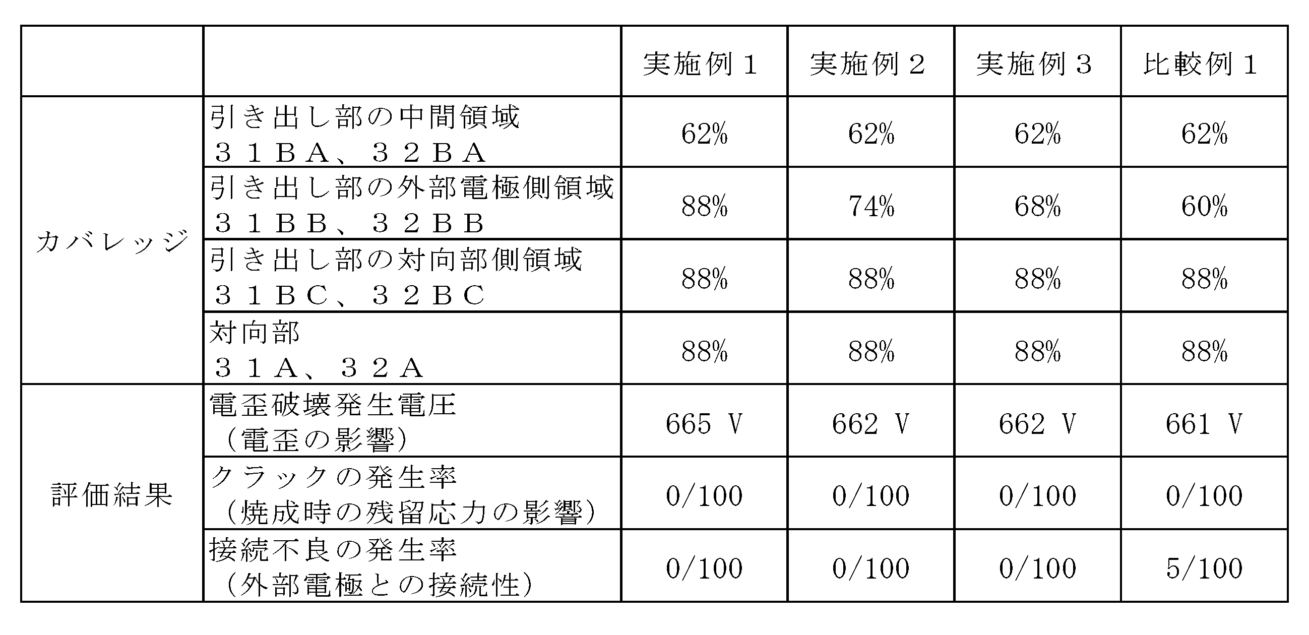
- the samples of Examples 1 to 3 are samples in which the coverage of the first intermediate region 31BA and the second intermediate region 32BA is lower than the coverage of the first external electrode side region 31BB and the second external electrode side region 32BB, and the coverage of the first intermediate region 31BA and the second intermediate region 31BAB is lower than the coverage of the first opposing portion 31A and the second opposing portion 32A.
- the coverage of the intermediate region of the samples of Examples 1 to 3 was 62%, and the coverage of the external electrode side region was 88%, 74%, and 68%, respectively.
- the sample of Comparative Example 1 has a coverage of 60% in the external electrode side region, and the coverage of the first external electrode side region 31BB and the second external electrode side region 32BB is lower than the coverage of the first intermediate region 31BA and the second intermediate region 32BA.
- the multilayer ceramic capacitors of Examples 1 to 3 in which the coverage of the intermediate region is lower than the coverage of the external electrode region and the coverage of the opposing region, can ensure capacitance density and maintain connectivity between the internal electrode layer and the external electrode while reducing stress concentration due to electrostrictive effects when voltage is applied. It is preferable that the coverage of the external electrode region is higher than the coverage of the intermediate region and is 68% or more.
- the samples of Examples 1 to 4 are samples in which the coverage of the first intermediate region 31BA and the second intermediate region 32BA is lower than the coverage of the first external electrode side region 31BB and the second external electrode side region 32BB, and the coverage of the first intermediate region 31BA and the second intermediate region 31BAB is lower than the coverage of the first opposing portion 31A and the second opposing portion 32A.
- the coverage of the intermediate region of the samples of Examples 1 to 4 was 62%, and the coverage of the opposing side region was 88%, 75%, 68%, and 64%.
- the multilayer ceramic capacitors of Examples 1 to 4 in which the coverage of the middle region is lower than the coverage of the external electrode side region and the coverage of the opposing portion, can ensure capacitance density and maintain connectivity between the internal electrode layer and the external electrode while reducing stress concentration due to electrostrictive effects when voltage is applied.
- the coverage of the opposing portion side region is higher than the coverage of the middle region, and is preferably 64% or more, and more preferably 68% or more. Note that when the coverage of the opposing portion side region is lowered, there was a tendency for residual stress to occur during firing.
- the samples of Examples 1 to 3 are samples in which the coverage of the first intermediate region 31BA and the second intermediate region 32BA is lower than the coverage of the first external electrode side region 31BB and the second external electrode side region 32BB, and the coverage of the first intermediate region 31BA and the second intermediate region 31BAB is lower than the coverage of the first opposing portion 31A and the second opposing portion 32A.
- the coverage of the intermediate region of the samples of Examples 1 to 3 was 62%, and the coverage of the opposing portions was 88%, 75%, and 71%, respectively.
- the multilayer ceramic capacitors of Examples 1 to 3 in which the coverage of the intermediate region is lower than the coverage of the external electrode region and the coverage of the opposing portion, can ensure capacitance density and maintain connectivity between the internal electrode layer and the external electrode while reducing stress concentration due to electrostrictive effects when voltage is applied.
- the coverage of the opposing portion is higher than the coverage of the intermediate region, and is preferably 71% or more, and more preferably 75% or more. Note that when the coverage of the opposing portion is lowered, there was a tendency for residual stress to occur during firing.
- the above describes an embodiment of the present invention, but the present invention is not limited to the embodiment, and can be implemented in various forms without departing from the gist of the present invention.
- the present invention includes the following combinations.
- ⁇ 2> The multilayer ceramic capacitor described in ⁇ 1>, in which the coverage of the first opposing side region and the second opposing side region is higher than the coverage of the first intermediate region and the second intermediate region.
- ⁇ 3> A multilayer ceramic capacitor according to ⁇ 1> or ⁇ 2>, in which the coverage of the first intermediate region and the second intermediate region is 55% or more.
- ⁇ 4> A multilayer ceramic capacitor according to ⁇ 1> to ⁇ 3>, in which the coverage of the first intermediate region and the second intermediate region is 80% or less.
Landscapes
- Engineering & Computer Science (AREA)
- Power Engineering (AREA)
- Manufacturing & Machinery (AREA)
- Microelectronics & Electronic Packaging (AREA)
- Chemical & Material Sciences (AREA)
- Materials Engineering (AREA)
- Ceramic Engineering (AREA)
- Inorganic Chemistry (AREA)
- Fixed Capacitors And Capacitor Manufacturing Machines (AREA)
- Ceramic Capacitors (AREA)
Abstract
Description
以下、図面を参照しながら本開示の第1実施形態に係る積層セラミックコンデンサ1について説明する。図1は、実施形態に係る積層セラミックコンデンサ1の外観斜視図である。図2は、図1のII-II断面図である。図3は、図2のIII-III断面図である。図4Aは、図2のIVA-IVA断面図である。図4Bは、図2のIVB-IVB断面図である。
以下、第2実施形態に係る積層セラミックコンデンサ1について説明する。なお、以下の説明において、第1実施形態と同じ構成については、同じ符号を付し、また詳細な説明を省略する。図6Aは、第2実施形態に係る積層セラミックコンデンサ1における図2のR1で示す部分を模式的に示す拡大断面図である。図6Bは、第2実施形態に係る積層セラミックコンデンサ1における図2のR2で示す部分を模式的に示す拡大断面図である。図6Aおよび図6Bは、LT断面の一部である。図6Aおよび図6Bにおいては、積層体10における誘電体層20、第1の内部電極層31、および第2の内部電極層32と、第1の外部電極40Aと、第2の外部電極40Bとが示されている。
カバレッジ(%)=(内部電極層の面積/分析対象範囲の面積)×100・・・(1)
実施形態に記載された製造方法にしたがって、内部電極層の各領域のカバレッジを調整して作製された複数のロットの積層セラミックコンデンサを各ロットの試料として作製した。その後、作製した試料を用いて、電歪による破壊発生電圧評価、クラックの発生の評価、内部電極と外部電極の接続性評価を行った。
・容量:2.2μF
・定格電圧:100V
・誘電体層:BaTiO3
・誘電体層の厚み:1μm
・内部電極層:Ni
・下地電極層:導電性金属(Cu)とガラス成分を含む電極
・めっき層:Niめっき層2μmおよびSnめっき層2μmの2層構造
・内部電極の引き出し部(端面側外層部(Lギャップ))のL方向長さ:220μm
電歪の発生の程度により、積層セラミックコンデンサの破壊発生電圧は変化する。よって、絶縁破壊電圧(BVD)を測定するBVD装置により、電歪の評価を行った。
まず、積層セラミックコンデンサの各試料の外部電極をBDV測定装置の電極に設置した。
次に、室温下において、初期電圧:0V、昇圧速度:100V/sec、検知電流(不良と判断する電流値の設定):10mAの条件で、電圧の印加を開始した。そして、検知電流を超える直前の電圧を記録し、この値を電歪破壊発生電圧とした。
実施例および比較例ごとに、20個の試料について評価を行い、その平均値を実施例および比較例の電歪破壊発生電圧とした。
積層セラミックコンデンサの焼成時の残留応力の影響によるクラックの発生の評価においては、各ロットの積層セラミックコンデンサをそれぞれ100個作製して実施した。
クラックの発生の有無は、積層体の中心を通るWT断面を研磨により露出させ、露出断面を光学顕微鏡にて観察することにより確認した。クラックの発生が確認された試料を、クラック発生試料(不良)としてカウントした。
内部電極と外部電極の接続性評価においては、各ロットの積層セラミックコンデンサをそれぞれ100個作製して実施した。
100個の試料について、100Vの定格電圧を印加した後にただちにショートさせる急速放電試験を行った。この後静電容量を測定し、急速放電試験前の静電容量値からの低下率を求めた。このとき、低下率が5%以上であったものを、急速放電試験により内部電極と外部電極の接続部において切れがある程度生じたものとして、接続不良が発生した試料(不良)としてカウントした。



10 積層体
20 誘電体層
30 内部電極層
31 第1の内部電極層
31A 第1の対向部
31B 第1の引き出し部
31BA 第1の中間領域
31BB 第1の外部電極側領域
31BC 第1の対向部側領域
32 第2の内部電極層
32A 第2の対向部
32B 第2の引き出し部
32BA 第2の中間領域
32BB 第2の外部電極側領域
32BC 第2の対向部側領域
40 外部電極
40A 第1の外部電極
40B 第2の外部電極
50 下地電極層
50A 第1の下地電極層
50B 第2の下地電極層
L 長さ方向
T 積層方向
W 幅方向
LS1 第1の端面
LS2 第2の端面
TS1 第1の主面
TS2 第2の主面
WS1 第1の側面
WS2 第2の側面
Claims (7)
- 積層された複数の誘電体層と積層された複数の内部電極層とを含み、積層方向に相対する第1の主面および第2の主面と、積層方向に直交する幅方向に相対する第1の側面および第2の側面と、積層方向および幅方向に直交する長さ方向に相対する第1の端面および第2の端面と、を含む積層体と、
前記第1の端面側に配置される第1の外部電極と、
前記第2の端面側に配置される第2の外部電極と、
を備える積層セラミックコンデンサであって、
前記複数の内部電極層は、第1の内部電極層および第2の内部電極層を含み、
前記第1の内部電極層は、その一方端部が前記第1の端面に引き出されて前記第1の外部電極と接続する第1の引き出し部と、前記第1の引き出し部に接続され、積層方向に隣り合って配置された前記第2の内部電極層と対向する第1の対向部とを有し、
前記第2の内部電極層は、その一方端部が前記第2の端面に引き出されて前記第2の外部電極と接続する第2の引き出し部と、前記第2の引き出し部に接続され、積層方向に隣り合って配置された前記第1の内部電極層と対向する第2の対向部とを有し、
前記第1の引き出し部は、前記第1の外部電極との接続部近傍の第1の外部電極側領域と、前記第1の対向部との接続部近傍の第1の対向部側領域と、前記第1の外部電極側領域と前記第1の対向部側領域との間にある第1の中間領域と、を有し、
前記第2の引き出し部は、前記第2の外部電極との接続部近傍の第2の外部電極側領域と、前記第2の対向部との接続部近傍の第2の対向部側領域と、前記第2の外部電極側領域と前記第2の対向部側領域との間にある第2の中間領域と、を有し、
前記第1の中間領域および前記第2の中間領域のカバレッジは、前記第1の外部電極側領域および前記第2の外部電極側領域のカバレッジよりも低く、
前記第1の中間領域および前記第2の中間領域のカバレッジは、前記第1の対向部および前記第2の対向部のカバレッジよりも低い、積層セラミックコンデンサ。 - 前記第1の対向部側領域および前記第2の対向部側領域のカバレッジは、前記第1の中間領域および前記第2の中間領域のカバレッジよりも高い、請求項1に記載の積層セラミックコンデンサ。
- 前記第1の中間領域のおよび前記第2の中間領域のカバレッジは、55%以上である、請求項1または請求項2に記載の積層セラミックコンデンサ。
- 前記第1の中間領域および前記第2の中間領域のカバレッジは、80%以下である、請求項1~3のいずれか1項に記載の積層セラミックコンデンサ。
- 前記第1の外部電極側領域および前記第2の外部電極側領域のカバレッジは、前記第1の中間領域および前記第2の中間領域のカバレッジよりも高く、かつ68%以上である、請求項1~4のいずれか1項に記載の積層セラミックコンデンサ。
- 前記第1の対向部側領域および前記第2の対向部側領域のカバレッジは、前記第1の中間領域および前記第2の中間領域のカバレッジよりも高く、かつ68%以上である、請求項1~5のいずれか1項に記載の積層セラミックコンデンサ。
- 前記第1の対向部および前記第2の対向部のカバレッジは、前記第1の中間領域および前記第2の中間領域のカバレッジよりも高く、かつ75%以上である、請求項1~6のいずれか1項に記載の積層セラミックコンデンサ。
Priority Applications (6)
| Application Number | Priority Date | Filing Date | Title |
|---|---|---|---|
| JP2025526952A JPWO2024257211A1 (ja) | 2023-06-13 | 2023-06-13 | |
| CN202380097310.7A CN120958538A (zh) | 2023-06-13 | 2023-06-13 | 层叠陶瓷电容器 |
| PCT/JP2023/021882 WO2024257211A1 (ja) | 2023-06-13 | 2023-06-13 | 積層セラミックコンデンサ |
| KR1020257033910A KR20250167648A (ko) | 2023-06-13 | 2023-06-13 | 적층 세라믹 콘덴서 |
| EP23921571.8A EP4730375A1 (en) | 2023-06-13 | 2023-06-13 | Multilayer ceramic capacitor |
| US18/805,970 US20240420893A1 (en) | 2023-06-13 | 2024-08-15 | Multilayer ceramic capacitor |
Applications Claiming Priority (1)
| Application Number | Priority Date | Filing Date | Title |
|---|---|---|---|
| PCT/JP2023/021882 WO2024257211A1 (ja) | 2023-06-13 | 2023-06-13 | 積層セラミックコンデンサ |
Related Child Applications (1)
| Application Number | Title | Priority Date | Filing Date |
|---|---|---|---|
| US18/805,970 Continuation US20240420893A1 (en) | 2023-06-13 | 2024-08-15 | Multilayer ceramic capacitor |
Publications (1)
| Publication Number | Publication Date |
|---|---|
| WO2024257211A1 true WO2024257211A1 (ja) | 2024-12-19 |
Family
ID=93844601
Family Applications (1)
| Application Number | Title | Priority Date | Filing Date |
|---|---|---|---|
| PCT/JP2023/021882 Ceased WO2024257211A1 (ja) | 2023-06-13 | 2023-06-13 | 積層セラミックコンデンサ |
Country Status (6)
| Country | Link |
|---|---|
| US (1) | US20240420893A1 (ja) |
| EP (1) | EP4730375A1 (ja) |
| JP (1) | JPWO2024257211A1 (ja) |
| KR (1) | KR20250167648A (ja) |
| CN (1) | CN120958538A (ja) |
| WO (1) | WO2024257211A1 (ja) |
Citations (6)
| Publication number | Priority date | Publication date | Assignee | Title |
|---|---|---|---|---|
| JPH08306580A (ja) | 1995-05-11 | 1996-11-22 | Murata Mfg Co Ltd | セラミック電子部品の製造方法及びセラミック電子部品 |
| JP2013016770A (ja) * | 2011-06-30 | 2013-01-24 | Samsung Electro-Mechanics Co Ltd | 積層セラミック電子部品及びその製造方法 |
| JP2014093517A (ja) * | 2012-11-05 | 2014-05-19 | Samsung Electro-Mechanics Co Ltd | 積層セラミック電子部品及びその製造方法 |
| JP2018152547A (ja) * | 2017-03-14 | 2018-09-27 | 株式会社村田製作所 | 積層セラミックコンデンサ |
| JP2021061302A (ja) * | 2019-10-04 | 2021-04-15 | 株式会社村田製作所 | 積層セラミックコンデンサ |
| JP2022191909A (ja) * | 2021-06-16 | 2022-12-28 | 株式会社村田製作所 | 積層セラミック電子部品 |
Family Cites Families (8)
| Publication number | Priority date | Publication date | Assignee | Title |
|---|---|---|---|---|
| JP4674456B2 (ja) * | 2004-10-19 | 2011-04-20 | 株式会社村田製作所 | 積層セラミック電子部品およびその製造方法 |
| KR101070095B1 (ko) * | 2009-12-10 | 2011-10-04 | 삼성전기주식회사 | 적층 세라믹 커패시터 및 그 제조방법 |
| KR20120043501A (ko) * | 2010-10-26 | 2012-05-04 | 삼성전기주식회사 | 적층 세라믹 전자부품 및 이의 제조방법 |
| JP5620938B2 (ja) * | 2012-03-30 | 2014-11-05 | 太陽誘電株式会社 | 積層セラミックコンデンサ |
| KR101883016B1 (ko) * | 2013-07-22 | 2018-07-27 | 삼성전기주식회사 | 적층 세라믹 전자부품 및 이의 제조방법 |
| JP2017108011A (ja) * | 2015-12-10 | 2017-06-15 | 株式会社村田製作所 | セラミックコンデンサ及びその製造方法 |
| JP7003889B2 (ja) * | 2018-10-10 | 2022-01-21 | 株式会社村田製作所 | 積層セラミック電子部品およびその実装構造 |
| JP2020072136A (ja) * | 2018-10-30 | 2020-05-07 | 株式会社村田製作所 | セラミック電子部品およびセラミック電子部品の製造方法 |
-
2023
- 2023-06-13 WO PCT/JP2023/021882 patent/WO2024257211A1/ja not_active Ceased
- 2023-06-13 CN CN202380097310.7A patent/CN120958538A/zh active Pending
- 2023-06-13 KR KR1020257033910A patent/KR20250167648A/ko active Pending
- 2023-06-13 EP EP23921571.8A patent/EP4730375A1/en active Pending
- 2023-06-13 JP JP2025526952A patent/JPWO2024257211A1/ja active Pending
-
2024
- 2024-08-15 US US18/805,970 patent/US20240420893A1/en active Pending
Patent Citations (6)
| Publication number | Priority date | Publication date | Assignee | Title |
|---|---|---|---|---|
| JPH08306580A (ja) | 1995-05-11 | 1996-11-22 | Murata Mfg Co Ltd | セラミック電子部品の製造方法及びセラミック電子部品 |
| JP2013016770A (ja) * | 2011-06-30 | 2013-01-24 | Samsung Electro-Mechanics Co Ltd | 積層セラミック電子部品及びその製造方法 |
| JP2014093517A (ja) * | 2012-11-05 | 2014-05-19 | Samsung Electro-Mechanics Co Ltd | 積層セラミック電子部品及びその製造方法 |
| JP2018152547A (ja) * | 2017-03-14 | 2018-09-27 | 株式会社村田製作所 | 積層セラミックコンデンサ |
| JP2021061302A (ja) * | 2019-10-04 | 2021-04-15 | 株式会社村田製作所 | 積層セラミックコンデンサ |
| JP2022191909A (ja) * | 2021-06-16 | 2022-12-28 | 株式会社村田製作所 | 積層セラミック電子部品 |
Also Published As
| Publication number | Publication date |
|---|---|
| KR20250167648A (ko) | 2025-12-01 |
| JPWO2024257211A1 (ja) | 2024-12-19 |
| EP4730375A1 (en) | 2026-04-22 |
| US20240420893A1 (en) | 2024-12-19 |
| CN120958538A (zh) | 2025-11-14 |
Similar Documents
| Publication | Publication Date | Title |
|---|---|---|
| CN115483030B (zh) | 层叠陶瓷电子部件 | |
| JP7517260B2 (ja) | 積層セラミック電子部品 | |
| JP7468498B2 (ja) | 積層セラミックコンデンサ | |
| JP7501564B2 (ja) | 積層セラミック電子部品 | |
| JP7585990B2 (ja) | 積層セラミック電子部品 | |
| CN117716457A (zh) | 层叠陶瓷电容器 | |
| JP7740567B2 (ja) | 積層セラミック電子部品 | |
| WO2024135256A1 (ja) | 積層セラミック電子部品 | |
| CN119256381A (zh) | 层叠陶瓷电容器 | |
| WO2024257211A1 (ja) | 積層セラミックコンデンサ | |
| WO2024257348A1 (ja) | 積層セラミックコンデンサ | |
| WO2024257347A1 (ja) | 積層セラミックコンデンサ | |
| CN116469685A (zh) | 层叠陶瓷电容器 | |
| JP7776002B2 (ja) | 積層セラミックコンデンサ | |
| JP2021125673A (ja) | 積層セラミックコンデンサ | |
| US20250391606A1 (en) | Multilayer ceramic capacitor | |
| KR102953790B1 (ko) | 적층 세라믹 콘덴서 | |
| US20250378999A1 (en) | Multilayer ceramic capacitor | |
| US20250372311A1 (en) | Multilayer ceramic capacitor | |
| WO2025126319A1 (ja) | 積層セラミック電子部品 | |
| WO2024224920A1 (ja) | 積層セラミックコンデンサ | |
| WO2024262134A1 (ja) | 積層セラミックコンデンサ | |
| WO2024257346A1 (ja) | 積層セラミックコンデンサ | |
| KR20250002661A (ko) | 적층 세라믹 콘덴서 | |
| WO2024257476A1 (ja) | 積層セラミックコンデンサ |
Legal Events
| Date | Code | Title | Description |
|---|---|---|---|
| WWE | Wipo information: entry into national phase |
Ref document number: 202417069102 Country of ref document: IN |
|
| 121 | Ep: the epo has been informed by wipo that ep was designated in this application |
Ref document number: 23921571 Country of ref document: EP Kind code of ref document: A1 |
|
| ENP | Entry into the national phase |
Ref document number: 2025526952 Country of ref document: JP Kind code of ref document: A |
|
| WWE | Wipo information: entry into national phase |
Ref document number: 2025526952 Country of ref document: JP |
|
| ENP | Entry into the national phase |
Ref document number: 1020257033910 Country of ref document: KR Free format text: ST27 STATUS EVENT CODE: A-0-1-A10-A15-NAP-PA0105 (AS PROVIDED BY THE NATIONAL OFFICE) |
|
| WWE | Wipo information: entry into national phase |
Ref document number: KR1020257033910 Country of ref document: KR Ref document number: 1020257033910 Country of ref document: KR |
|
| WWP | Wipo information: published in national office |
Ref document number: 1020257033910 Country of ref document: KR |
|
| WWE | Wipo information: entry into national phase |
Ref document number: 2023921571 Country of ref document: EP |
|
| NENP | Non-entry into the national phase |
Ref country code: DE |
|
| ENP | Entry into the national phase |
Ref document number: 2023921571 Country of ref document: EP Effective date: 20260113 |
|
| ENP | Entry into the national phase |
Ref document number: 2023921571 Country of ref document: EP Effective date: 20260113 |
|
| ENP | Entry into the national phase |
Ref document number: 2023921571 Country of ref document: EP Effective date: 20260113 |
|
| ENP | Entry into the national phase |
Ref document number: 2023921571 Country of ref document: EP Effective date: 20260113 |