WO2024257475A1 - 光学系、画像投写装置および撮像装置 - Google Patents
光学系、画像投写装置および撮像装置 Download PDFInfo
- Publication number
- WO2024257475A1 WO2024257475A1 PCT/JP2024/015229 JP2024015229W WO2024257475A1 WO 2024257475 A1 WO2024257475 A1 WO 2024257475A1 JP 2024015229 W JP2024015229 W JP 2024015229W WO 2024257475 A1 WO2024257475 A1 WO 2024257475A1
- Authority
- WO
- WIPO (PCT)
- Prior art keywords
- optical system
- reflecting surface
- optical
- point
- sub
- Prior art date
- Legal status (The legal status is an assumption and is not a legal conclusion. Google has not performed a legal analysis and makes no representation as to the accuracy of the status listed.)
- Ceased
Links
Images










Classifications
-
- G—PHYSICS
- G02—OPTICS
- G02B—OPTICAL ELEMENTS, SYSTEMS OR APPARATUS
- G02B13/00—Optical objectives specially designed for the purposes specified below
- G02B13/18—Optical objectives specially designed for the purposes specified below with lenses having one or more non-spherical faces, e.g. for reducing geometrical aberration
-
- G—PHYSICS
- G02—OPTICS
- G02B—OPTICAL ELEMENTS, SYSTEMS OR APPARATUS
- G02B13/00—Optical objectives specially designed for the purposes specified below
- G02B13/16—Optical objectives specially designed for the purposes specified below for use in conjunction with image converters or intensifiers, or for use with projectors, e.g. objectives for projection TV
-
- G—PHYSICS
- G02—OPTICS
- G02B—OPTICAL ELEMENTS, SYSTEMS OR APPARATUS
- G02B17/00—Systems with reflecting surfaces, with or without refracting elements
- G02B17/08—Catadioptric systems
-
- G—PHYSICS
- G02—OPTICS
- G02B—OPTICAL ELEMENTS, SYSTEMS OR APPARATUS
- G02B17/00—Systems with reflecting surfaces, with or without refracting elements
- G02B17/08—Catadioptric systems
- G02B17/0856—Catadioptric systems comprising a refractive element with a reflective surface, the reflection taking place inside the element, e.g. Mangin mirrors
-
- G—PHYSICS
- G02—OPTICS
- G02B—OPTICAL ELEMENTS, SYSTEMS OR APPARATUS
- G02B27/00—Optical systems or apparatus not provided for by any of the groups G02B1/00 - G02B26/00, G02B30/00
- G02B27/09—Beam shaping, e.g. changing the cross-sectional area, not otherwise provided for
- G02B27/0938—Using specific optical elements
- G02B27/095—Refractive optical elements
- G02B27/0972—Prisms
-
- G—PHYSICS
- G03—PHOTOGRAPHY; CINEMATOGRAPHY; ANALOGOUS TECHNIQUES USING WAVES OTHER THAN OPTICAL WAVES; ELECTROGRAPHY; HOLOGRAPHY
- G03B—APPARATUS OR ARRANGEMENTS FOR TAKING PHOTOGRAPHS OR FOR PROJECTING OR VIEWING THEM; APPARATUS OR ARRANGEMENTS EMPLOYING ANALOGOUS TECHNIQUES USING WAVES OTHER THAN OPTICAL WAVES; ACCESSORIES THEREFOR
- G03B21/00—Projectors or projection-type viewers; Accessories therefor
-
- G—PHYSICS
- G03—PHOTOGRAPHY; CINEMATOGRAPHY; ANALOGOUS TECHNIQUES USING WAVES OTHER THAN OPTICAL WAVES; ELECTROGRAPHY; HOLOGRAPHY
- G03B—APPARATUS OR ARRANGEMENTS FOR TAKING PHOTOGRAPHS OR FOR PROJECTING OR VIEWING THEM; APPARATUS OR ARRANGEMENTS EMPLOYING ANALOGOUS TECHNIQUES USING WAVES OTHER THAN OPTICAL WAVES; ACCESSORIES THEREFOR
- G03B21/00—Projectors or projection-type viewers; Accessories therefor
- G03B21/14—Details
-
- G—PHYSICS
- G03—PHOTOGRAPHY; CINEMATOGRAPHY; ANALOGOUS TECHNIQUES USING WAVES OTHER THAN OPTICAL WAVES; ELECTROGRAPHY; HOLOGRAPHY
- G03B—APPARATUS OR ARRANGEMENTS FOR TAKING PHOTOGRAPHS OR FOR PROJECTING OR VIEWING THEM; APPARATUS OR ARRANGEMENTS EMPLOYING ANALOGOUS TECHNIQUES USING WAVES OTHER THAN OPTICAL WAVES; ACCESSORIES THEREFOR
- G03B21/00—Projectors or projection-type viewers; Accessories therefor
- G03B21/14—Details
- G03B21/28—Reflectors in projection beam
Definitions
- This disclosure relates to an optical system using a prism. This disclosure also relates to an image projection device and an imaging device using such an optical system.
- Patent documents 1 to 3 disclose optical systems that use prisms to enable short-focus, large-screen projection or imaging.
- This disclosure provides an optical system that enables short-focus, large-screen projection or imaging in an oblique direction. This disclosure also provides an image projection device and imaging device that use such an optical system.
- One aspect of the present disclosure is an optical system having a reduction conjugate point on a reduction side and a magnification conjugate point on a magnification side, and having intermediate image positions therein that are conjugates to the reduction conjugate point and the magnification conjugate point,
- a first sub-optical system including a plurality of lenses that are rotationally symmetric with respect to an optical axis along the Z direction and an aperture between the plurality of lenses;
- a second sub-optical system including a prism having a plurality of optical surfaces, the second sub-optical system being disposed on the enlargement side of the first sub-optical system;
- the prism has, as the plurality of optical surfaces, a first transmitting surface, a first reflecting surface, a second reflecting surface, and a second transmitting surface, in that order from the reduction side to the enlargement side, and inside the prism, a light ray travels within a YZ plane that includes the Z direction and a Y direction perpendicular to the Z direction;
- Another aspect of the present disclosure is an optical system having a reduction conjugate point on a reduction side and a magnification conjugate point on a magnification side, and having intermediate image positions therein that are conjugates to the reduction conjugate point and the magnification conjugate point, respectively, and the reduction conjugate point has an image-forming relationship in a rectangular area having a first direction and a second direction, a first sub-optical system including a plurality of lenses through which the light beam passes and an aperture stop between two lenses of the plurality of lenses; a second sub-optical system including a prism, the second sub-optical system being disposed on the enlargement side of the first sub-optical system;
- the prism is A first transmitting surface located on the reduction side and a second transmitting surface located on the enlargement side; a first reflecting surface and a second reflecting surface are included in an optical path from the first transmitting surface to the second transmitting surface, When a plane including the position where the chief ray of a first light beam that passes through a point
- An image projection device includes the above optical system and an image forming element that generates an image to be projected onto a screen via the optical system.
- An imaging device includes the above optical system and an imaging element that receives an optical image formed by the optical system and converts it into an electrical image signal.
- the optical system disclosed herein makes it easier to manufacture prisms and also makes it possible to miniaturize prisms with free-form surfaces. It also makes it possible to project or capture images in an oblique direction toward a magnified conjugate point.
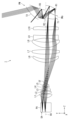
- FIG. 1 is a layout diagram showing an optical system 1 according to a first embodiment.
- Fig. 2A is a perspective view showing the three-dimensional shape of each optical surface of the prism PM, and Fig. 2B shows a part of a light ray traveling inside the prism PM.
- Fig. 3A is a cross-sectional view of the prism PM along the YZ plane, and Fig. 3B shows a part of a light ray traveling inside the prism PM.
- Fig. 4A is a top view of the prism PM as viewed from the Y direction, and Fig. 4B shows a part of a light beam traveling inside the prism PM.
- Fig. 2A is a perspective view showing the three-dimensional shape of each optical surface of the prism PM
- Fig. 2B shows a part of a light ray traveling inside the prism PM.
- Fig. 3A is a cross-sectional view of the prism PM along the YZ plane
- Fig. 3B shows
- FIG. 5A is a YZ cross-sectional view for explaining the definitions of the first point on the first transmitting surface T1, the second point on the second reflecting surface R2, and the angle of incidence of the light beam on the second reflecting surface R2.
- Fig. 5B is a YZ cross-sectional view for explaining the definitions of the distances PL1 and PL2.
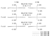
- 4A to 4C are lateral aberration diagrams of the optical system 1 according to Example 1.
- FIG. 11 is a layout diagram showing an optical system 1 according to a second embodiment.
- 5A to 5C are lateral aberration diagrams of the optical system 1 according to Example 2.
- FIG. 11 is a layout diagram showing an optical system 1 according to a third embodiment.
- 9A to 9C are lateral aberration diagrams of the optical system 1 according to Example 3.
- FIG. 11A shows a state in which the image projection device 100 is installed on the lower surface of a ceiling CE
- Fig. 11B shows a state in which the image projection device 100 is installed on the upper surface of a ceiling CE.
- 12A and 12B are diagrams for explaining the definition of variables in equation (6), respectively.
- FIG. 13 is a layout diagram showing an optical system 1 according to a fourth embodiment.
- Fig. 14A is a front perspective view showing the three-dimensional shape of each optical surface of the prism PM
- Fig. 14B is a rear perspective view showing the three-dimensional shape of each optical surface of the prism PM
- Fig. 14C is a side view showing the three-dimensional shape of the prism PM.
- Fig. 14A is a front perspective view showing the three-dimensional shape of each optical surface of the prism PM
- Fig. 14B is a rear perspective view showing the three-dimensional shape of each optical surface of the prism PM
- Fig. 14C is a side view showing the three-dimensional
- Fig. 15A is a side view showing the relative positions of the first transmitting surface T1, the second transmitting surface T2, the first reflecting surface R1, the second reflecting surface R2, and the third reflecting surface R3, and Fig. 15B is a side view showing a part of a light ray traveling inside the prism PM.
- Fig. 16A is a top view showing the relative positions of the first transmitting surface T1, the second transmitting surface T2, the first reflecting surface R1, the second reflecting surface R2, and the third reflecting surface R3 as viewed from the Y direction
- Fig. 16B is a top view showing a part of a light ray traveling inside the prism PM.
- FIG. 1 is a YZ cross-sectional view showing a state in which the first light beam LF1 and the second light beam LF2 travel through the first transmitting surface T1, the second transmitting surface T2, the first reflecting surface R1, the second reflecting surface R2, and the third reflecting surface R3 in this order.
- 5 is an explanatory diagram showing the relationship between a first footprint area FP1 of a first light flux LF1 and a second footprint area FP2 of a second light flux LF2 on a second reflecting surface R2.
- FIG. 13 is an explanatory diagram showing the relationship between a third footprint area FP3 of the first light flux LF1 and a fourth footprint area FP4 of the second light flux LF2 on a third reflecting surface R3.
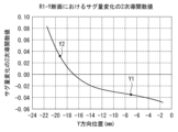
- FIG. 13 is a graph showing the second derivative value of the change in sag amount in the Y cross section of the first reflecting surface R1.
- 11A to 11C are lateral aberration diagrams of the optical system 1 according to Example 4.
- 11A to 11C are lateral aberration diagrams of the optical system 1 according to Example 4.
- 11A to 11C are lateral aberration diagrams of the optical system 1 according to Example 4.
- FIG. 13 is a layout diagram showing an optical system 1 according to a fifth embodiment.
- 13A to 13C are lateral aberration diagrams of the optical system 1 according to Example 5.
- 13A to 13C are lateral aberration diagrams of the optical system 1 according to Example 5.
- 13A to 13C are lateral aberration diagrams of the optical system 1 according to Example 5. This corresponds to FIG.
- FIG. 9 is a block diagram illustrating an example of an image projection device according to the present disclosure.
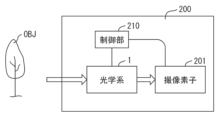
- FIG. 1 is a block diagram illustrating an example of an imaging device according to the present disclosure.
- the optical system is used in a projector (one example of an image projection device) that projects onto a screen the image light of an original image SA, which is formed by spatially modulating incident light using an image forming element such as a liquid crystal or a DMD (digital micromirror device) based on an image signal. That is, the optical system according to the present disclosure can be used to enlarge and project onto a screen an original image SA on an image forming element arranged on the reduction side by arranging a screen (not shown) on an extension of the enlargement side.
- the projection surface is not limited to a screen. Projection surfaces also include walls, ceilings, floors, and windows inside homes and stores, or vehicles and aircraft used for mobile transportation.
- the optical system disclosed herein can also be used to collect light emitted from an object located on the extension of the magnification side and form an optical image of the object on the imaging surface of an imaging element located on the reduction side.
- Example 1 Fig. 1 is a layout diagram showing an optical system 1 according to Example 1.
- the optical system 1 includes a first sub-optical system including an aperture stop ST and a second sub-optical system including a prism PM.
- a reduction conjugate point which is an imaging position on the reduction side, is located on the right side of the optical axis OA
- a magnification conjugate point which is an imaging position on the magnification side
- the second sub-optical system is provided on the magnification side of the first sub-optical system.
- both the Y-direction intermediate image IMy and the X-direction intermediate image IMx exist within the prism PM.
- the Y-direction intermediate image IMy is shown in Figure 1, but the X-direction intermediate image IMx is not shown.
- the first sub-optical system includes, from the reduction side to the enlargement side, an optical element PA and lens elements L1 to L7.
- the optical element PA represents an optical element such as a TIR (total internal reflection) prism, a prism for color separation and color synthesis, an optical filter, a parallel plate glass, a quartz low-pass filter, and an infrared cut filter.
- a reduction conjugate point is set at a position a predetermined distance from the reduction side end face of the optical element PA, and the original image SA is placed here (surface 23).
- surface 23 For the surface numbers, refer to the numerical example described later.
- Optical element PA has two parallel, flat transmitting surfaces (surfaces 21, 22).
- Lens element L1 has a biconvex shape (surfaces 19, 20).
- Lens element L2 has a biconvex shape (surfaces 17, 18).
- Lens element L3 has a biconcave shape (surfaces 15, 16).
- Lens element L4 has a biconvex shape (surfaces 13, 14).
- Lens element L5 has a biconvex shape (surfaces 9, 10).
- Lens element L6 has a positive meniscus shape with the convex surface facing the reduction side (surfaces 7, 8).
- Lens element L7 has a biconcave shape (surfaces 5, 6).
- These lens elements L1 to L7 are rotationally symmetric lenses having surface shapes that are rotationally symmetric around the optical axis OA of the first sub-optical system, and portions through which light rays do not pass may be removed if necessary.
- the second sub-optical system includes a prism PM formed of a transparent medium, such as glass or synthetic resin.
- the prism PM has a first transmitting surface T1 located on the reduction side, a second transmitting surface T2 located on the enlargement side, and two reflecting surfaces, a first reflecting surface R1 and a second reflecting surface R2, located on the optical path between the first transmitting surface T1 and the second transmitting surface T2, as a plurality of optical surfaces.
- the first transmitting surface T1 has a free-form shape with a convex surface facing the reduction side (surface 4).
- the first reflecting surface R1 has a free-form shape with a concave surface facing the direction in which the light ray incident on the first reflecting surface R1 is reflected (surface 3).
- the second reflecting surface R2 has a free-form shape with a convex surface facing the direction in which the light ray incident on the second reflecting surface R2 is reflected (surface 2).
- the second transmitting surface T2 has a free-form shape with a convex surface facing the enlargement side (surface 1).
- the aperture stop ST defines the range through which the light beam passes through the optical system 1, and is positioned between the reduction conjugate point and the intermediate image position described above.
- the aperture stop ST is located between lens element L4 and lens element L5 (surface 12).
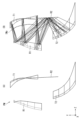
- Figure 2(A) is a perspective view showing the three-dimensional shape of each optical surface of the prism PM, and Figure 2(B) shows a portion of the light rays traveling inside the prism PM.
- Figure 3(A) is a cross-sectional view of the prism PM along the YZ plane, and Figure 3(B) shows a portion of the light rays traveling inside the prism PM.
- Figure 4(A) is a top view of the prism PM as seen from the Y direction, and Figure 4(B) shows a portion of the light rays traveling inside the prism PM.
- FIG. 5(A) is a YZ cross-sectional view explaining the definitions of the first point on the first transmitting surface T1, the second point on the second reflecting surface R2, and the angle of incidence of the light ray on the second reflecting surface R2.
- FIG. 5(B) is a YZ cross-sectional view explaining the definitions of the distances PL1 and PL2. Details will be described later.
- FIG. 6 is a lateral aberration diagram of the optical system 1 according to Example 1.
- the solid line represents a wavelength of 550.0000 nm
- the dashed line represents a wavelength of 610.0000 nm
- the dashed line represents a wavelength of 455.0000 nm. It can be seen from these graphs that the optical system 1 according to Example 1 exhibits excellent optical performance.
- Example 2 Fig. 7 is a layout diagram showing an optical system 1 according to Example 2.
- This optical system 1 has a configuration similar to that of Example 1, and a description that overlaps with Example 1 will be omitted.
- the optical system 1 includes a first sub-optical system including an aperture stop ST and a second sub-optical system including a prism PM.
- a reduction conjugate point which is an imaging position on the reduction side, is located on the right side of the optical axis OA
- a magnification conjugate point which is an imaging position on the magnification side
- the second sub-optical system is provided on the magnification side of the first sub-optical system.
- both the Y-direction intermediate image IMy and the X-direction intermediate image IMx exist within the prism PM.
- the Y-direction intermediate image IMy is shown in Figure 7, but the X-direction intermediate image IMx is not shown.
- the second reflecting surface R2 has a free-form shape with a convex surface facing the direction in which the light ray incident on the second reflecting surface R2 is reflected (surface 2).
- the second transmitting surface T2 has a free-form shape with a convex surface facing the enlargement side (surface 1).
- FIG. 8 is a lateral aberration diagram of the optical system 1 according to Example 2.
- both the Y-direction intermediate image IMy and the X-direction intermediate image IMx exist within the prism PM.
- the Y-direction intermediate image IMy is shown in Figure 9, but the X-direction intermediate image IMx is not shown.
- Optical element PA has two parallel, flat transmitting surfaces (surfaces 21, 22).
- Lens element L1 has a positive meniscus shape with the convex surface facing the reduction side (surfaces 19, 20).
- Lens element L2 has a biconvex shape (surfaces 17, 18).
- Lens element L3 has a biconcave shape (surfaces 15, 16).
- Lens element L4 has a biconvex shape (surfaces 13, 14).
- Lens element L5 has a positive meniscus shape with the convex surface facing the reduction side (surfaces 9, 10).
- Lens element L6 has a positive meniscus shape with the convex surface facing the reduction side (surfaces 7, 8).
- Lens element L7 has a biconcave shape (surfaces 5, 6).
- the prism PM has a first transmitting surface T1 located on the reduction side, a second transmitting surface T2 located on the enlargement side, and two reflecting surfaces, a first reflecting surface R1 and a second reflecting surface R2, located on the optical path between the first transmitting surface T1 and the second transmitting surface T2.
- the first transmitting surface T1 has a free-form shape with a convex surface facing the reduction side (surface 4).
- the first reflecting surface R1 has a free-form shape with a concave surface facing the direction in which the light ray incident on the first reflecting surface R1 is reflected (surface 3).
- the second reflecting surface R2 has a free-form shape with a convex surface facing the direction in which the light ray incident on the second reflecting surface R2 is reflected (surface 2).
- the second transmitting surface T2 has a free-form shape with a convex surface facing the enlargement side (surface 1).
- FIG. 10 is a lateral aberration diagram of the optical system 1 according to Example 3.
- Example 4 Fig. 13 is a layout diagram showing an optical system 1 according to Example 4.
- the optical system 1 includes a first sub-optical system including an aperture stop ST and a second sub-optical system including a prism PM.
- a reduction conjugate point which is an imaging position on the reduction side, is located to the left of the optical axis OA
- a magnification conjugate point which is an imaging position on the magnification side, is located diagonally above the prism PM.
- the second sub-optical system is provided on the magnification side of the first sub-optical system.
- both the Y-direction intermediate image IMy and the X-direction intermediate image IMx exist within the prism PM.
- the Y-direction intermediate image IMy is shown in Figure 13, but the X-direction intermediate image IMx is not shown.
- the first sub-optical system includes, from the reduction side to the enlargement side, optical element PA and lens elements L1 to L10.
- Optical element PA represents optical elements such as a TIR (total internal reflection) prism, a prism for color separation and color synthesis, an optical filter, parallel plate glass, a quartz low-pass filter, and an infrared cut filter.
- a reduction conjugate point is set at a position a predetermined distance from the reduction side end face of optical element PA1, where the original image SA is placed (surface 0). Note that for the surface numbers, refer to the numerical examples described later.
- Optical element PA has two parallel, flat transmissive surfaces (surfaces 1, 2).
- Lens element L1 has a biconvex shape (surfaces 3, 4).
- Lens element L2 has a biconvex shape (surfaces 5, 6).
- Lens element L3 has a biconcave shape (surfaces 7, 8).
- Lens element L4 has a biconcave shape (surfaces 9, 10).
- Lens element L5 has a biconvex shape (surfaces 11, 12).
- Lens element L6 has a positive meniscus shape with the convex surface facing the reduction side (surfaces 15, 16).
- Lens element L7 has a biconvex shape (surfaces 17, 18).
- Lens element L8 has a positive meniscus shape with the convex surface facing the reduction side (surfaces 19, 20).
- Lens element L9 has a biconcave shape (surfaces 21, 22).
- Lens element L10 has a negative meniscus shape with the convex surface facing the reduction side (surfaces 23, 24).
- These lens elements L1 to L10 are rotationally symmetric lenses that have a surface shape that is rotationally symmetric around the optical axis OA of the first sub-optical system, and if necessary, portions through which light rays do not pass may be removed.
- the second sub-optical system includes a prism PM formed of a transparent medium, such as glass or synthetic resin.
- the prism PM has a first transmitting surface T1 located on the reduction side, a second transmitting surface T2 located on the enlargement side, and three reflecting surfaces R1, R2, and R3 located on the optical path between the first transmitting surface T1 and the second transmitting surface T2 as a plurality of optical surfaces.
- the first transmitting surface T1 has a free-form shape with a convex surface facing the reduction side (surface 25).
- the first reflecting surface R1 has a free-form shape with a convex surface and a concave surface facing in the direction in which the light ray incident on the first reflecting surface R1 is reflected (surface 26).
- the second reflecting surface R2 has a free-form shape with a concave surface facing in the direction in which the light ray incident on the second reflecting surface R2 is reflected (surface 27).
- the third reflecting surface R3 has a free-form shape with a convex surface facing in the direction in which the light ray incident on the third reflecting surface R3 is reflected (surface 28).
- the second transmitting surface T2 has a free-form shape with a convex surface facing the magnification side (surface 29).
- the aperture stop ST defines the range through which the light beam passes through the optical system 1, and is positioned between the reduction conjugate point and the intermediate image position described above.
- the aperture stop ST is located between lens element L5 and lens element L6 (surface 13).
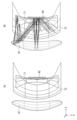
- FIG. 14(A) is a front perspective view showing the three-dimensional shape of each optical surface of the prism PM.
- FIG. 14(B) is a rear perspective view showing the three-dimensional shape of each optical surface of the prism PM.
- FIG. 14(C) is a side view showing the three-dimensional shape of the prism PM.
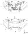
- FIG. 15(A) is a side view showing the relative positions of the first transmitting surface T1, the second transmitting surface T2, the first reflecting surface R1, the second reflecting surface R2, and the third reflecting surface R3.
- FIG. 15(B) is a side view showing a portion of the light beam traveling inside the prism PM.
- FIG. 15(B) is a side view showing a portion of the light beam traveling inside the prism PM.
- FIG. 16(A) is a top view seen from the Y direction showing the relative positions of the first transmitting surface T1, the second transmitting surface T2, the first reflecting surface R1, the second reflecting surface R2, and the third reflecting surface R3.
- FIG. 16(B) is a top view showing a portion of the light beam traveling inside the prism PM.
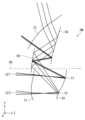
- FIG. 17 is a YZ cross-sectional view showing the first light beam LF1 and the second light beam LF2 traveling through the first transmitting surface T1, the second transmitting surface T2, the first reflecting surface R1, the second reflecting surface R2, and the third reflecting surface R3 in that order.
- FIGS. 18(A) and 18(B) are explanatory diagrams showing the relationship between the first footprint area FP1 of the first light beam LF1 and the second footprint area FP2 of the second light beam LF2 on the second reflecting surface R2.
- FIG. 19 is an explanatory diagram showing the relationship between the third footprint area FP3 of the first light beam LF1 and the fourth footprint area FP4 of the second light beam LF2 on the third reflecting surface R3.
- FIG. 20 is a graph showing the second derivative value of the sag amount change in the Y cross-section on the first reflecting surface R1. These will be described in detail later.
- 21 to 23 are lateral aberration diagrams of the optical system 1 according to Example 4.
- the solid line indicates a wavelength of 550.0000 nm
- the dashed line indicates a wavelength of 610.0000 nm
- the dashed line indicates a wavelength of 455.0000 nm. From these graphs, it can be seen that the optical system 1 according to Example 4 exhibits excellent optical performance.
- FIG. 24 is a layout diagram showing an optical system 1 according to Example 5.
- This optical system 1 has a configuration similar to that of Example 4, and a description that overlaps with Example 4 will be omitted.
- the optical system 1 includes a first sub-optical system including an aperture stop ST and a second sub-optical system including a prism PM.
- a reduction conjugate point which is an imaging position on the reduction side, is located to the left of the optical axis OA
- a magnification conjugate point which is an imaging position on the magnification side, is located diagonally above the prism PM.
- the second sub-optical system is provided on the magnification side of the first sub-optical system.
- both the Y-direction intermediate image IMy and the X-direction intermediate image IMx exist within the prism PM.
- the Y-direction intermediate image IMy is shown in Figure 24, but the X-direction intermediate image IMx is not shown.
- the first sub-optical system includes, in order from the reduction side to the enlargement side, an optical element PA and lens elements L1 to L10.
- a reduction conjugate point is set at a position a predetermined distance from the reduction side end face of the optical element PA, and the original image SA is placed here (surface 0).
- surface 0 For the surface numbers, refer to the numerical examples described later.
- Optical element PA has two parallel, flat transmissive surfaces (surfaces 1 and 2).
- Lens element L1 has a biconvex shape (surfaces 3 and 4).
- Lens element L2 has a biconvex shape (surfaces 5 and 6).
- Lens element L3 has a biconcave shape (surfaces 7 and 8).
- Lens element L4 has a biconcave shape (surfaces 9 and 10).
- Lens element L5 has a biconvex shape (surfaces 11 and 12).
- Lens element L6 has a positive meniscus shape with the convex surface facing the reduction side (surfaces 15 and 16).
- Lens element L7 has a biconvex shape (surfaces 17 and 18).
- Lens element L8 has a positive meniscus shape with the convex surface facing the reduction side (surfaces 19 and 20).
- Lens element L9 has a biconcave shape (surfaces 21 and 22).
- Lens element L10 has a negative meniscus shape with the convex surface facing the reduction side (surfaces 23 and 24).
- These lens elements L1 to L10 are rotationally symmetric lenses that have a surface shape that is rotationally symmetric around the optical axis OA of the first sub-optical system, and if necessary, portions through which light rays do not pass may be removed.
- the prism PM has a plurality of optical surfaces, including a first transmitting surface T1 located on the reduction side, a second transmitting surface T2 located on the enlargement side, and three reflecting surfaces R1, R2, and R3 located on the optical path between the first transmitting surface T1 and the second transmitting surface T2.
- the first transmitting surface T1 has a free-form shape with a convex surface facing the reduction side (surface 25).
- the first reflecting surface R1 has a free-form shape with a convex surface and a concave surface facing in the direction in which the light ray incident on the first reflecting surface R1 is reflected (surface 26).
- the second reflecting surface R2 has a free-form shape with a concave surface facing in the direction in which the light ray incident on the second reflecting surface R2 is reflected (surface 27).
- the third reflecting surface R3 has a free-form shape with a convex surface facing in the direction in which the light ray incident on the third reflecting surface R3 is reflected (surface 28).
- the second transmitting surface T2 has a free-form shape with a convex surface facing the magnification side (surface 29).
- FIGS. 25 to 27 are lateral aberration diagrams of the optical system 1 according to Example 5.
- Figure 28 corresponds to Figure 9 attached to the basic application of the priority right of this application (Japanese Patent Application No. 2023-198654), and is an explanatory diagram showing the shape of the footprint on the first reflecting surface R1 and the second reflecting surface R2 in Examples 1 to 3 of the basic application.
- the first principal ray passes through a position close to the lower end of the first reflecting surface R1, and then passes through a position close to the upper end of the second reflecting surface R2.
- the second principal ray passes through a position close to the upper end of the first reflecting surface R1, and then passes through a position close to the center of the second reflecting surface R2.
- the footprint of the first principal ray tends to be larger than the footprint of the second principal ray, and this tendency is particularly large on the second reflecting surface R2.
- footprint A located at the center of the first principal ray overlaps with footprint B located at the center of the second principal ray.
- the optical system according to this embodiment has a reduction conjugate point on the reduction side and a magnification conjugate point on the magnification side, and has intermediate image positions therein that are conjugates to the reduction conjugate point and the magnification conjugate point, respectively.
- a first sub-optical system including a plurality of lenses that are rotationally symmetric with respect to an optical axis OA along the Z direction, and an aperture between the plurality of lenses;
- a second sub-optical system including a prism PM having a plurality of optical surfaces, the second sub-optical system being disposed on the enlargement side of the first sub-optical system;
- the prism PM has, as the plurality of optical surfaces, a first transmitting surface T1, a first reflecting surface R1, a second reflecting surface R2, and a second transmitting surface T2, in that order from the reduction side to the enlargement side, and inside the prism PM, a light ray travels within a YZ plane that includes the Z direction and a Y direction perpen
- the prism PM has, as optical surfaces, a first transmitting surface T1, a first reflecting surface R1, a second reflecting surface R2, and a second transmitting surface T2, in that order from the reduction side to the enlargement side.
- a distance FL1 between the point on the first reflecting surface R1 farthest from the perpendicular line of the optical axis OA passing through the apex of the optical surface on the most enlargement side of the first sub-optical system and the perpendicular line, and a distance FL2 between the point on the second transmitting surface T2 farthest from the perpendicular line and the perpendicular line can be defined.
- the first reflecting surface R1 needs a certain distance between the first transmitting surface T1 and the first reflecting surface R1 in order to reflect the multiple light beams incident from the first sub-optical system to the second reflecting surface R2.
- the optical system can be shortened in the Z direction by designing the distance FL2 to be smaller than the distance FL1, and as a result, the prism PM can be made smaller.
- a distance PL1 parallel to the Z direction between a point on the first transmitting surface T1 closest to the perpendicular line and a point on the first reflecting surface R1 farthest from the perpendicular line, and a distance PL2 parallel to the Z direction between a point on the second reflecting surface R2 closest to the perpendicular line and a point on the second transmitting surface T2 farthest from the perpendicular line may be smaller than the distance PL1.
- the prism can be made smaller in the Z direction. Furthermore, when performing shift projection in the Y direction, the second transmitting surface T2 tends to become larger in the Y direction. Therefore, by reducing the size of the second transmitting surface T2 in the Z direction, it is also possible to prevent the prism from becoming larger in the Y direction.
- may be smaller than the Y coordinate interval
- represents the absolute value of x.
- FIG. 5(A) shows only the light beam closest to the optical axis OA and its chief ray PR among all the light rays passing through or reflected from the effective area of the optical surface.
- the YZ coordinates (yt1, zt1) of the first point through which the chief ray PR passes on the first transmitting surface T1 can be defined.
- the YZ coordinates (yr2, zr2) of the second point where the chief ray PR is reflected on the second reflecting surface R2 can be defined.
- the arrangement of the first transmitting surface T1 and the second reflecting surface R2 is designed so that when comparing the YZ coordinates of both,
- the Z coordinate zt1 of the first point is located on the +Z side (right side of FIG. 5A) of the Z coordinate zr2 of the second point.
- the Z coordinate zt1 of the first point may be located on the -Z side (left side of FIG. 5A) of the Z coordinate zr2 of the second point.
- the Z coordinate zt1 of the first point and the Z coordinate zr2 of the second point may be the same, in which case it is sufficient that the Z coordinate interval
- ( 0) is smaller than the Y coordinate interval
- a distance PL1 can be defined that is parallel to the optical axis OA of the first sub-optical system between the point on the first transmitting surface T1 that is closest to the perpendicular to the optical axis OA passing through the apex (the intersection of the optical surface and the optical axis) of the optical surface (the enlarged side surface of lens element L7) that is closest to the enlarged optical surface of the first sub-optical system, and the point on the first reflecting surface R1 that is farthest from that perpendicular.
- a distance PL2 can be defined that is parallel to the optical axis OA of the first sub-optical system between the point on the second reflecting surface R2 that is closest to the perpendicular and the point on the second transmitting surface T2 that is farthest from that perpendicular.
- the arrangement of the first transmitting surface T1, the first reflecting surface R1, the second reflecting surface R2, and the second transmitting surface T2 is designed so that the distance PL2 is smaller than the distance PL1.
- the first transmitting surface T1 and the second reflecting surface R2 can be maintained nearly perpendicular to the optical axis OA, making it easy to manufacture the prism PM. Conversely, if the first transmitting surface T1 and the second reflecting surface R2 are tilted too much with respect to the optical axis OA, it becomes difficult to manufacture the prism PM. In addition, because the first transmitting surface T1 and the second reflecting surface R2 are close to each other in the Z direction and the distance PL2 is smaller than the distance PL1, it becomes possible to miniaturize a prism with a free-form surface.
- the optical system according to this embodiment may satisfy the following expressions (1) and (2). 0.5 ⁇ PL2/PL1 ⁇ 0.8...(1)
- the optical system according to this embodiment may satisfy the following formula (3). 0.5 ⁇ r2 ⁇ 3.0...(3) Where: ⁇ r2: the angle (unit: °) between the normal at the position of the second reflecting surface R2 on which the principal ray PR of the light beam closest to the optical axis OA is incident and the normal to the conjugate surface including the reduction conjugate point It is.
- the chief ray PR of the light beam closest to the optical axis OA is reflected by the first reflecting surface R1 and then enters the second point (yr2, zr2) on the second reflecting surface R2.
- the normal NA at the second point (yr2, zr2) can be defined.
- the normal NR of the conjugate plane including the reduction conjugate point can be defined. This normal NR can generally be set parallel to the optical axis OA of the optical system.
- the optical system according to this embodiment may satisfy the following formula (4). 0.0 ⁇ rt1x/rt1y ⁇ 0.8...(4) Where: rt1x: partial radius of curvature in the x direction of the first transmitting surface T1 at the first point, rt1y: partial radius of curvature in the y direction of the first transmitting surface T1 at the first point.
- the YZ coordinates (yt1, zt1) of the first point through which the principal ray PR passes have a partial radius of curvature rt1x in the x direction and a partial radius of curvature rt1y in the y direction.
- equation (4) it is possible to achieve oblique projection or imaging to the magnified conjugate point while suppressing astigmatism at the magnified conjugate point.
- the optical system according to this embodiment may satisfy the following formula (5). 15 ⁇ i2m ⁇ 30...(5)
- ⁇ i2m the angle of incidence at which the chief ray PR of the light beam closest to the optical axis OA is incident on the second reflecting surface R2 (unit: °) It is.
- the chief ray PR of the light beam closest to the optical axis OA is reflected by the first reflecting surface R1 and then enters the second point (yr2, zr2) on the second reflecting surface R2.
- the angle of incidence of the chief ray PR on the second reflecting surface R2 can be defined as the angle of incidence ⁇ i2m between the normal NA at the second point and the traveling direction of the chief ray PR. Therefore, by making the angle of incidence ⁇ i2m satisfy the formula (5), it is possible to suppress the curvature of field at the magnification conjugate point while achieving oblique projection or imaging of a large-screen image perpendicular to the optical axis OA to the magnification conjugate point.
- the optical system in the Z direction, is disposed between a reduction conjugate plane formed at the position of the reduction conjugate point and a magnification conjugate plane formed at the position of the magnification conjugate point, and the reduction conjugate plane and the magnification conjugate plane may be parallel to each other.
- the light rays that project a large-screen image perpendicular to the optical axis OA at an angle toward the screen do not pass around the optical system. This makes it possible to install any components around the optical system, for example, to hide the optical system from the view of the audience.
- the optical system according to this embodiment may satisfy the following formula (6).
- D Distance between the magnified conjugate point and the optical system
- V Length in a first direction parallel to the vertical direction to the magnified conjugate point perpendicular to the optical axis of the effective area where all light rays are projected or imaged on the conjugate plane including the magnified conjugate point
- H Length in a second direction perpendicular to the vertical direction of the effective area where all light rays are projected or imaged on the conjugate plane including the magnified conjugate point
- SF Vertical distance from the optical axis to the center of the first direction length of the effective area.
- FIG. 11(A) when an optical system is mounted on an image projection device 100 and oblique projection is performed toward a screen SR (magnified conjugate point), the image projection device 100 is generally often installed on the underside of a ceiling CE. The audience views the image projected onto the screen SR, but is also aware of the presence of the image projection device 100.
- FIG. 11(B) it is possible to imagine that the image projection device 100 is installed on the upper surface of the ceiling CE and performs oblique projection toward the screen SR. In this case, the image projection device 100 is hidden by the ceiling CE, making it difficult for the audience to recognize the presence of the image projection device 100, and they can immerse themselves in viewing the image.
- an optical system capable of projection in a diagonal direction that is greatly inclined with respect to the screen SR of a large-screen image perpendicular to the optical axis OA is required.
- FIGs 11(A) and 11(B) an example is shown in which the image projection device 100 is installed on the ceiling CE side and an image is projected downward, but alternatively, the image projection device 100 may be installed on the floor side and an image may be projected diagonally upward. Also, the image projection device 100 may be installed on the side wall of the room (the right or left wall) and an image may be projected diagonally horizontally (to the left or right).
- FIG. 12 is a diagram for explaining the definition of the variables in equation (6), with FIG. 12(A) showing a YZ cross section and FIG. 12(B) showing a ZX cross section.
- the optical system can satisfy equation (6) when the distance between the screen SR and the optical system of the image projection device 100 is D, the length of the effective area on the screen SR onto which all the light rays are projected in a second direction perpendicular to the direction perpendicular to the magnified conjugate point perpendicular to the optical axis OA is H, the length of the effective area on the screen SR onto which all the light rays are projected in a first direction parallel to the vertical direction is V, and the vertical distance from the optical axis OA to the center of the length of the effective area in the first direction is SF.
- a configuration can be realized in which the projection distance D to the screen SR is small (so-called short focus projection) and the vertical distance SF is large (so-called super shift projection).
- a first footprint area on the second reflecting surface of a first light beam that is closest to the optical axis on the first transmitting surface may overlap a second footprint area on the second reflecting surface of a second light beam that is farthest from the optical axis on the first transmitting surface.
- the first light beam LF1 closest to the optical axis OA on the first transmitting surface T1 forms a first footprint area FP1 on the second reflecting surface R2.
- the second light beam LF2 farthest from the optical axis OA on the first transmitting surface T1 forms a second footprint area FP2 on the second reflecting surface R2.
- the area for the second footprint area FP2 can be reduced to reduce the size of the second reflecting surface R2, and the size of the prism PM in the Y direction can also be suppressed.
- the area of the second footprint area FP2 overlapping with the first footprint area FP1 can be reduced to reduce the size of the second reflecting surface R2, and the size of the prism PM in the Y direction can also be suppressed.
- the optical system according to the present embodiment has a reduction conjugate point on the reduction side and a magnification conjugate point on the magnification side, and has intermediate image positions therein that are conjugates to the reduction conjugate point and the magnification conjugate point, respectively, and the reduction conjugate point has an image-forming relationship in a rectangular area having a first direction and a second direction, a first sub-optical system including a plurality of lenses through which the light beam passes and an aperture stop between two lenses of the plurality of lenses; a second sub-optical system including a prism PM, the second sub-optical system being disposed on the enlargement side of the first sub-optical system;
- the prism PM is A first transmitting surface T1 located on the reduction side, and a second transmitting surface T2 located on the enlargement side, an optical path from the first transmitting surface T1 to the second transmitting surface T2 includes a first reflecting surface R2 and a second reflecting surface R2 in that order;
- the prism PM has, as its optical surfaces, a first transmitting surface T1, a first reflecting surface R1, a second reflecting surface R2, a third reflecting surface R3 and a second transmitting surface T2, in that order from the reduction side to the enlargement side.
- a prism PM having three reflecting surfaces R1 to R3 is illustrated as an example, but the prism PM may have one, two, or four or more reflecting surfaces.
- the first light beam LF1 passing through a point closest to the optical axis OA forms a first footprint area FP1 on the second reflecting surface R2.
- the second light beam LF2 passing through a point farthest from the optical axis OA forms a second footprint area FP2 on the second reflecting surface R2.
- the area for the second footprint area FP2 can be reduced, the size of the second reflecting surface R2 can be reduced, and the size of the prism PM in the Y direction can be suppressed.
- the area of the second footprint area FP2 overlapping the first footprint area FP1 can be reduced, and the size of the second reflecting surface R2 can be suppressed, and the size of the prism PM in the Y direction can be suppressed.
- the first reflecting surface R1 may have a curved shape that imparts positive power at Y1, where Y1 is the position at which the chief ray of the first light beam LF1 is reflected.
- the first reflecting surface R1 has a curved shape that imparts positive power P1. This makes it possible to reduce the size of the first footprint area FP1 formed by the first light beam LF1 on the second reflecting surface R2. As a result, the prism PM can be made smaller.
- the first reflecting surface R1 may have a curved shape such that, when the position at which the chief ray of the second light beam FL2 is reflected is Y2, the power imparted at Y2 is smaller than the positive power imparted at Y1.
- the first reflecting surface R1 may have a curved shape that is given negative power at Y2.
- the first reflecting surface R1 has a negative power P2 at position Y2.
- optical performance at a low throw ratio can be ensured.
- the range in which the second derivative value of the sag amount change in the Y cross section is a positive value indicates negative power P2, and the range in which the second derivative value is a negative value indicates positive power P1.
- Such a curved shape can be designed as a free-form shape defined by (Equation 2) and (Equation 3) described below.
- the optical system according to this embodiment may have a third reflecting surface R3 on the optical path between the second reflecting surface R2 and the second transmitting surface T1.
- the prism PM has three reflecting surfaces R1 to R3 on the optical path between the first transmitting surface T1 and the second transmitting surface T2. As a result, it is possible to achieve both a compact prism and a low throw ratio.
- the second reflecting surface R2 has a concave shape toward the inside of the prism, and therefore functions to converge the light beam.
- the third reflecting surface R3 has a convex shape toward the inside of the prism, and therefore functions to diverge the light beam. As a result, it is possible to achieve both a compact prism and a low throw ratio.
- the first footprint area FP1 may be located within a central 70% range of the second footprint area FP2.
- the longitudinal size of the second footprint area FP2 is A, and the first footprint area FP1 is included within the range of -A ⁇ 35% to +A ⁇ 35% from the center of the second footprint area FP2. This allows the size of the second reflecting surface R2 to be reduced, resulting in a more compact prism.
- the size ratio of the second footprint area FP to the first footprint area FP may be 20% or less.
- the longitudinal size of the second footprint area FP2 is A
- the longitudinal size of the first footprint area FP1 is set to A x 20% or less. This allows the size of the second reflecting surface R2 to be reduced, resulting in a more compact prism.
- the optical system according to this embodiment has a third reflecting surface R3 on an optical path between the second reflecting surface R2 and the second transmitting surface T2, and on the third reflecting surface R3, a third footprint area FP3 of the first light flux LF1 is located closer to the optical axis OA of the first sub-optical system than a fourth footprint area FP4 of the second light flux LF2,
- a size ratio of the third footprint region FP3 to the fourth footprint region FP4 may be 20% or less.
- the first light beam LF1 passing through the point closest to the optical axis OA forms a third footprint area FP3 on the third reflecting surface R3.
- the second light beam LF2 passing through the point farthest from the optical axis OA forms a fourth footprint area FP4 on the third reflecting surface R3.
- the third footprint area FP3 is located closer to the optical axis OA than the fourth footprint area FP4, and the longitudinal size of the fourth footprint area FP4 is set to B x 20% or less. This allows the size of the second reflecting surface R2 to be reduced, resulting in a more compact prism.
- the prism PM may have a shape such that, when the prism PM is viewed from the first sub-optical system, the second reflecting surface R2 is located between the first transmitting surface T1 and the second transmitting surface T2 in the Y cross section.
- a first transmitting surface T1, a second reflecting surface R2, and a second transmitting surface T2 are arranged in front of the prism PM, and a first reflecting surface R1 and a second reflecting surface R2 are arranged behind the prism PM.
- this optical system is used in an image projection device, rear projection can be achieved in which image light from an image forming element enters the first transmitting surface T1 and is emitted diagonally upward from the second transmitting surface T2.
- z sag amount of a surface parallel to the z axis
- c curvature at the vertex of the surface
- k Conic coefficient
- a to H 4th to 18th order coefficients of r.
- the free-form surface shape is expressed as a local Cartesian coordinate system (x, y, z) with the vertex of the surface as the origin. It is defined by the following formula using
- z Sag amount of the surface parallel to the z axis
- c curvature at the surface vertex
- k conic coefficient
- C j coefficient of the monomial x my n .
- the i-th term of x and the j-th term of y which are the free-form surface coefficients in the polynomial, are written as x**i*y**j.
- "X**2*Y” indicates that the free-form surface coefficients are the quadratic term of x and the linear term of y in the polynomial.
- Table 10 below shows the corresponding values of formulas (1) to (6) in each of Numerical Examples 1 to 3.
- formula (6) when a large-screen image perpendicular to the optical axis OA is projected obliquely toward the screen, the image-forming element is often also shifted in the Y direction from the optical axis PA as necessary.
- examples are shown in which the shift amounts of the image-forming element in the Y direction are -7.182 mm and -9.018 mm, respectively. That is, in FIG. 1, the center position of the original image SA of the image-forming element is shifted downward by 7.182 mm and 9.018 mm with respect to the optical axis OA.
- FIG. 29 is a block diagram showing an example of an image projection device according to the present disclosure.
- the image projection device 100 includes the optical system 1 disclosed in the first embodiment, an image forming element 101, a light source 102, a control unit 110, and the like.
- the image forming element 101 is composed of a liquid crystal, a DMD, or the like, and generates an image to be projected on the screen SR via the optical system 1.
- the light source 102 is composed of an LED (light emitting diode), a laser, or the like, and supplies light to the image forming element 101.
- the control unit 110 is composed of a CPU or an MPU, or the like, and controls the entire device and each component.
- the optical system 1 may be configured as an interchangeable lens that can be detachably attached to the image projection device 100, or may be configured as an integrated lens integrated into the image projection device 100.
- the image projection device 100 described above is capable of short-focus, large-screen projection using a compact device thanks to the optical system 1 of embodiment 1.
- FIG. 30 is a block diagram showing an example of an imaging device according to the present disclosure.
- the imaging device 200 includes the optical system 1 disclosed in the first embodiment, an imaging element 201, a control unit 210, and the like.
- the imaging element 201 is composed of a CCD (charge-coupled device) image sensor, a CMOS image sensor, and the like, and receives an optical image of an object OBJ formed by the optical system 1 and converts it into an electrical image signal.
- the control unit 110 is composed of a CPU or an MPU, and controls the entire device and each component.
- the optical system 1 may be configured as an interchangeable lens that can be detachably attached to the imaging device 200, or may be configured as a built-in lens integrated into the imaging device 200.
- the imaging device 200 described above uses the optical system 1 according to embodiment 1, making it possible to capture images with a short focal length and a large screen using a small device.
- the components shown in the attached drawings and detailed description may include not only components essential for solving the problem, but also components that are not essential for solving the problem in order to illustrate the above technology. Therefore, the fact that these non-essential components are shown in the attached drawings or detailed description should not be used to immediately conclude that these non-essential components are essential.
- This disclosure is applicable to image projection devices such as projectors and head-up displays, as well as imaging devices such as digital still cameras, digital video cameras, surveillance cameras in surveillance systems, web cameras, and vehicle-mounted cameras.
- this disclosure is applicable to imaging optical systems that require high image quality, such as projectors, digital still camera systems, and digital video camera systems.
Landscapes
- Physics & Mathematics (AREA)
- General Physics & Mathematics (AREA)
- Optics & Photonics (AREA)
- Lenses (AREA)
Abstract
本開示は、縮小側の縮小共役点および拡大側の拡大共役点を有し、これらとそれぞれ共役である中間結像位置を内部に有する光学系であって、光軸に関して回転対称である複数のレンズおよび絞りを有する第1サブ光学系と、プリズムを含む第2サブ光学系とを備える。プリズムは、縮小側から拡大側へ順に第1透過面、第1反射面、第2反射面および第2透過面を有する。光学面の有効領域に関して、第1サブ光学系の最も拡大側にある光学面の面頂を通る光軸の垂線から最も遠い前記第1反射面の点と前記垂線との間の距離FL1と、前記垂線から最も遠い前記第2透過面の点と垂線との間の距離FL2において、前記距離FL2が前記距離FL1より小さい。
Description
本開示は、プリズムを用いた光学系に関する。また本開示は、こうした光学系を用いた画像投写装置および撮像装置に関する。
特許文献1~3は、プリズムを用いて短焦点かつ大画面の投写または撮像が可能になる光学系を開示する。
本開示は、短焦点かつ大画面の斜め方向の投写または撮像が可能になる光学系を提供する。また本開示は、こうした光学系を用いた画像投写装置および撮像装置を提供する。
本開示の一態様は、縮小側の縮小共役点および拡大側の拡大共役点を有し、該縮小共役点および該拡大共役点とそれぞれ共役である中間結像位置を内部に有する光学系であって、
Z方向に沿った光軸に関して回転対称である複数のレンズ、および前記複数のレンズの間に絞りを有する第1サブ光学系と、
前記第1サブ光学系より前記拡大側に配置され、複数の光学面を有するプリズムを含む第2サブ光学系と、を備え、
前記プリズムは、前記複数の光学面として、前記縮小側から前記拡大側へ順に第1透過面、第1反射面、第2反射面および第2透過面を有し、前記プリズムの内部において前記Z方向および前記Z方向に対して垂直なY方向を含むYZ面内で光線が進行し、
前記光軸に最も近い光線の前記中間結像位置は、前記第1透過面と前記第1反射面の間に配置され、
前記第1反射面は、前記第2反射面より強い正のパワーを有し、
前記複数の光学面の有効領域に関して前記YZ面において、
前記第1サブ光学系の最も拡大側にある光学面の面頂を通る前記光軸の垂線から最も遠い前記第1反射面の点と前記垂線との間の距離FL1と、前記垂線から最も遠い前記第2透過面の点と垂線との間の距離FL2において、前記距離FL2が前記距離FL1より小さい。
Z方向に沿った光軸に関して回転対称である複数のレンズ、および前記複数のレンズの間に絞りを有する第1サブ光学系と、
前記第1サブ光学系より前記拡大側に配置され、複数の光学面を有するプリズムを含む第2サブ光学系と、を備え、
前記プリズムは、前記複数の光学面として、前記縮小側から前記拡大側へ順に第1透過面、第1反射面、第2反射面および第2透過面を有し、前記プリズムの内部において前記Z方向および前記Z方向に対して垂直なY方向を含むYZ面内で光線が進行し、
前記光軸に最も近い光線の前記中間結像位置は、前記第1透過面と前記第1反射面の間に配置され、
前記第1反射面は、前記第2反射面より強い正のパワーを有し、
前記複数の光学面の有効領域に関して前記YZ面において、
前記第1サブ光学系の最も拡大側にある光学面の面頂を通る前記光軸の垂線から最も遠い前記第1反射面の点と前記垂線との間の距離FL1と、前記垂線から最も遠い前記第2透過面の点と垂線との間の距離FL2において、前記距離FL2が前記距離FL1より小さい。
本開示の他の一態様は、縮小側の縮小共役点および拡大側の拡大共役点を有し、該縮小共役点および該拡大共役点とそれぞれ共役である中間結像位置を内部に有し、前記縮小共役点は、第1方向と第2方向を有する矩形領域において結像関係を有する光学系であって、
光束が通過する複数のレンズと、前記複数のレンズの内の2枚のレンズの間の開口絞りを含む第1サブ光学系と、
該第1サブ光学系より拡大側に設けられ、プリズムを含む第2サブ光学系とを備え、
前記プリズムは、
縮小側に位置する第1透過面と、拡大側に位置する第2透過面と、
前記第1透過面から前記第2透過面に至る光路の順に、第1反射面および第2反射面を含み、
前記矩形領域で前記第1サブ光学系の光軸に最も近い点を通る第1光束の主光線が前記第1反射面で反射する位置と、前記第1サブ光学系の光軸とを含む平面をY断面とし、前記Y断面と前記矩形領域とが交わる線上で、前記第1サブ光学系の光軸から最も遠い点を通る光線を第2光束としたとき、前記第2反射面において、前記第1光束の第1フットプリント領域が前記第2光束の第2フットプリント領域に重なる。
光束が通過する複数のレンズと、前記複数のレンズの内の2枚のレンズの間の開口絞りを含む第1サブ光学系と、
該第1サブ光学系より拡大側に設けられ、プリズムを含む第2サブ光学系とを備え、
前記プリズムは、
縮小側に位置する第1透過面と、拡大側に位置する第2透過面と、
前記第1透過面から前記第2透過面に至る光路の順に、第1反射面および第2反射面を含み、
前記矩形領域で前記第1サブ光学系の光軸に最も近い点を通る第1光束の主光線が前記第1反射面で反射する位置と、前記第1サブ光学系の光軸とを含む平面をY断面とし、前記Y断面と前記矩形領域とが交わる線上で、前記第1サブ光学系の光軸から最も遠い点を通る光線を第2光束としたとき、前記第2反射面において、前記第1光束の第1フットプリント領域が前記第2光束の第2フットプリント領域に重なる。
また、本開示の他の一態様に係る画像投写装置は、上記光学系と、該光学系を経由してスクリーンに投写する画像を生成する画像形成素子と、を備える。
また、本開示の他の一態様に係る撮像装置は、上記光学系と、該光学系が形成する光学像を受光して電気的な画像信号に変換する撮像素子と、を備える。
本開示に係る光学系によると、プリズムの製造が容易になり、しかも自由曲面を有するプリズムの小型化が可能になる。また、拡大共役点に向けて斜め方向の投写または撮像が可能になる。
以下、適宜図面を参照しながら、実施の形態を詳細に説明する。但し、必要以上に詳細な説明は省略する場合がある。例えば、既によく知られた事項の詳細説明、あるいは実質的に同一の構成に対する重複説明を省略する場合がある。これは、以下の説明が不必要に冗長になるのを避け、当業者の理解を容易にするためである。
なお、出願人は、当業者が本開示を十分に理解するために添付図面および以下の説明を提供するのであって、これらによって請求の範囲に記載の主題を限定することを意図するものでない。
以下に、本開示に係る光学系の各実施例について説明する。各実施例では、光学系が、画像信号に基づき液晶やDMD(デジタルマイクロミラーデバイス)等の画像形成素子によって入射光を空間変調した原画像SAの画像光を、スクリーンに投写するプロジェクタ(画像投写装置の一例)に用いられる場合について説明する。即ち、本開示に係る光学系は、拡大側の延長線上に図示しないスクリーンを配置して、縮小側に配置された画像形成素子上の原画像SAを拡大してスクリーンに投写するために利用できる。ただし、被投写面はスクリーンに限定するものではない。住宅や店舗、または移動交通手段に用いられる車両や機内の壁や天井や床、窓なども被投写面に含む。
また、本開示に係る光学系は、拡大側の延長線上に位置する物体から放射される光を集光し、縮小側に配置された撮像素子の撮像面に物体の光学像を形成するためにも利用できる。
(実施形態1)
以下、図1~図28を用いて本開示の実施形態1に係る光学系について説明する。
以下、図1~図28を用いて本開示の実施形態1に係る光学系について説明する。
(実施例1)
図1は、実施例1に係る光学系1を示す配置図である。光学系1は、開口絞りSTを含む第1サブ光学系と、プリズムPMを含む第2サブ光学系とを備える。図1において、光軸OAの右側に縮小側の結像位置である縮小共役点が位置し、光軸OAの左下側に拡大側の結像位置である拡大共役点が位置する。第2サブ光学系は、第1サブ光学系より拡大側に設けられる。
図1は、実施例1に係る光学系1を示す配置図である。光学系1は、開口絞りSTを含む第1サブ光学系と、プリズムPMを含む第2サブ光学系とを備える。図1において、光軸OAの右側に縮小側の結像位置である縮小共役点が位置し、光軸OAの左下側に拡大側の結像位置である拡大共役点が位置する。第2サブ光学系は、第1サブ光学系より拡大側に設けられる。
また、光学系1の内部には、縮小共役点および拡大共役点とそれぞれ共役である中間結像位置が位置する。この中間結像位置は、プリズムPMの内部においてY方向中間像IMyとX方向中間像IMxの両方が存在する。Y方向中間像IMyは図1に示しているが、X方向中間像IMxは図示を省略している。
第1サブ光学系は縮小側から拡大側へと順に、光学素子PAと、レンズ素子L1~L7とを含む。光学素子PAは、TIR(total internal reflection)プリズム、色分解、色合成用のプリズム、光学フィルタ、平行平板ガラス、水晶ローパスフィルタ、赤外カットフィルタ等の光学素子を表している。光学素子PAの縮小側端面から所定距離の位置に縮小共役点が設定され、ここに原画像SAが設置される(面23)。なお面番号については、後述する数値実施例を参照する。
光学素子PAは、平行かつ平坦な2つの透過面を有する(面21,22)。レンズ素子L1は、両凸形状を有する(面19,20)。レンズ素子L2は、両凸形状を有する(面17,18)。レンズ素子L3は、両凹形状を有する(面15,16)。レンズ素子L4は、両凸形状を有する(面13,14)。レンズ素子L5は、両凸形状を有する(面9,10)。レンズ素子L6は、縮小側に凸面を向けた正メニスカス形状を有する(面7,8)。レンズ素子L7は、両凹形状を有する(面5,6)。これらのレンズ素子L1~L7は、第1サブ光学系の光軸OAの周りに回転対称な面形状を有する回転対称レンズであり、必要に応じて、光線が通過しない部分は削除しても構わない。
第2サブ光学系は、透明な媒質、例えば、ガラス、合成樹脂などで形成されたプリズムPMを含む。プリズムPMは、複数の光学面として、縮小側に位置する第1透過面T1と、拡大側に位置する第2透過面T2と、第1透過面T1と第2透過面T2との間の光路上に位置する2つの第1反射面R1および第2反射面R2を有する。第1透過面T1は、縮小側に凸面を向けた自由曲面形状を有する(面4)。第1反射面R1は、第1反射面R1へ入射する光線が反射する方向に凹面を向けた自由曲面形状を有する(面3)。第2反射面R2は、第2反射面R2へ入射する光線が反射する方向に凸面を向けた自由曲面形状を有する(面2)。第2透過面T2は、拡大側に凸面を向けた自由曲面形状を有する(面1)。
開口絞りSTは、光学系1を光束が通過する範囲を規定するものであり、縮小共役点と上述した中間結像位置との間に位置決めされる。一例として、開口絞りSTは、レンズ素子L4とレンズ素子L5との間に位置する(面12)。
図2(A)は、プリズムPMの各光学面の立体形状を示す斜視図であり、図2(B)は、プリズムPMの内部を進行する光線の一部を示す。図3(A)は、YZ面に沿ったプリズムPMの断面図であり、図3(B)は、プリズムPMの内部を進行する光線の一部を示す。図4(A)は、Y方向から見たプリズムPMの上面図であり、図4(B)は、プリズムPMの内部を進行する光線の一部を示す。
図5(A)は、第1透過面T1での第1点、第2反射面R2での第2点および第2反射面R2での光線の入射角の定義を説明するYZ断面図である。図5(B)は、距離PL1,PL2の定義を説明するYZ断面図である。詳細は後述する。
図6は、実施例1に係る光学系1の横収差図である。各グラフは、縮小共役点における第1矩形有効領域の正規化座標(X,Y)=(1.00,1.00),(1.00,0.56),(1.00,0.12),(0.00,1.00),(0.00,0.56),(0.00,0.12)にそれぞれ対応する。実線は波長550.0000nm、破線は波長610.0000nm、一点鎖線は波長455.0000nmである。これらのグラフから、実施例1に係る光学系1は優れた光学性能を示すことが判る。
(実施例2)
図7は、実施例2に係る光学系1を示す配置図である。この光学系1は、実施例1と同様な構成を有しており、実施例1と重複する説明は省略する。光学系1は、開口絞りSTを含む第1サブ光学系と、プリズムPMを含む第2サブ光学系とを備える。図7において、光軸OAの右側に縮小側の結像位置である縮小共役点が位置し、光軸OAの左下側に拡大側の結像位置である拡大共役点が位置する。第2サブ光学系は、第1サブ光学系より拡大側に設けられる。
図7は、実施例2に係る光学系1を示す配置図である。この光学系1は、実施例1と同様な構成を有しており、実施例1と重複する説明は省略する。光学系1は、開口絞りSTを含む第1サブ光学系と、プリズムPMを含む第2サブ光学系とを備える。図7において、光軸OAの右側に縮小側の結像位置である縮小共役点が位置し、光軸OAの左下側に拡大側の結像位置である拡大共役点が位置する。第2サブ光学系は、第1サブ光学系より拡大側に設けられる。
また、光学系1の内部には、縮小共役点および拡大共役点とそれぞれ共役である中間結像位置が位置する。この中間結像位置は、プリズムPMの内部においてY方向中間像IMyとX方向中間像IMxの両方が存在する。Y方向中間像IMyは図7に示しているが、X方向中間像IMxは図示を省略している。
第1サブ光学系は縮小側から拡大側へと順に、光学素子PAと、レンズ素子L1~L7とを含む。光学素子PAの縮小側端面から所定距離の位置に縮小共役点が設定され、ここに原画像SAが設置される(面23)。なお面番号については、後述する数値実施例を参照する。
光学素子PAは、平行かつ平坦な2つの透過面を有する(面21,22)。レンズ素子L1は、縮小側に凸面を向けた正メニスカス形状を有する(面19,20)。レンズ素子L2は、両凸形状を有する(面17,18)。レンズ素子L3は、両凹形状を有する(面15,16)。レンズ素子L4は、両凸形状を有する(面13,14)。レンズ素子L5は、縮小側に凸面を向けた正メニスカス形状を有する(面9,10)。レンズ素子L6は、縮小側に凸面を向けた正メニスカス形状を有する(面7,8)。レンズ素子L7は、両凹形状を有する(面5,6)。これらのレンズ素子L1~L7は、光軸OAの周りに回転対称な面形状を有する回転対称レンズであり、必要に応じて、光線が通過しない部分は削除しても構わない。
プリズムPMは、縮小側に位置する第1透過面T1と、拡大側に位置する第2透過面T2と、第1透過面T1と第2透過面T2との間の光路上に位置する2つの第1反射面R1および第2反射面R2を有する。第1透過面T1は、縮小側に凸面を向けた自由曲面形状を有する(面4)。第1反射面R1は、第1反射面R1へ入射する光線が反射する方向に凹面を向けた自由曲面形状を有する(面3)。第2反射面R2は、第2反射面R2へ入射する光線が反射する方向に凸面を向けた自由曲面形状を有する(面2)。第2透過面T2は、拡大側に凸面を向けた自由曲面形状を有する(面1)。
図8は、実施例2に係る光学系1の横収差図である。各グラフは、縮小共役点における第1矩形有効領域の正規化座標(X,Y)=(1.00,1.00),(1.00,0.56),(1.00,0.12),(0.00,1.00),(0.00,0.56),(0.00,0.12)にそれぞれ対応する。これらのグラフから、実施例2に係る光学系1は優れた光学性能を示すことが判る。
(実施例3)
図9は、実施例3に係る光学系1を示す配置図である。この光学系1は、実施例1と同様な構成を有しており、実施例1と重複する説明は省略する。光学系1は、開口絞りSTを含む第1サブ光学系と、プリズムPMを含む第2サブ光学系とを備える。図9において、光軸OAの右側に縮小側の結像位置である縮小共役点が位置し、光軸OAの左下側に拡大側の結像位置である拡大共役点が位置する。第2サブ光学系は、第1サブ光学系より拡大側に設けられる。
図9は、実施例3に係る光学系1を示す配置図である。この光学系1は、実施例1と同様な構成を有しており、実施例1と重複する説明は省略する。光学系1は、開口絞りSTを含む第1サブ光学系と、プリズムPMを含む第2サブ光学系とを備える。図9において、光軸OAの右側に縮小側の結像位置である縮小共役点が位置し、光軸OAの左下側に拡大側の結像位置である拡大共役点が位置する。第2サブ光学系は、第1サブ光学系より拡大側に設けられる。
また、光学系1の内部には、縮小共役点および拡大共役点とそれぞれ共役である中間結像位置が位置する。この中間結像位置は、プリズムPMの内部においてY方向中間像IMyとX方向中間像IMxの両方が存在する。Y方向中間像IMyは図9に示しているが、X方向中間像IMxは図示を省略している。
第1サブ光学系は縮小側から拡大側へと順に、光学素子PAと、レンズ素子L1~L7とを含む。光学素子PAの縮小側端面から所定距離の位置に縮小共役点が設定され、ここに原画像SAが設置される(面23)。なお面番号については、後述する数値実施例を参照する。
光学素子PAは、平行かつ平坦な2つの透過面を有する(面21,22)。レンズ素子L1は、縮小側に凸面を向けた正メニスカス形状を有する(面19,20)。レンズ素子L2は、両凸形状を有する(面17,18)。レンズ素子L3は、両凹形状を有する(面15,16)。レンズ素子L4は、両凸形状を有する(面13,14)。レンズ素子L5は、縮小側に凸面を向けた正メニスカス形状を有する(面9,10)。レンズ素子L6は、縮小側に凸面を向けた正メニスカス形状を有する(面7,8)。レンズ素子L7は、両凹形状を有する(面5,6)。これらのレンズ素子L1~L7は、光軸OAの周りに回転対称な面形状を有する回転対称レンズであり、必要に応じて、光線が通過しない部分は削除しても構わない。
プリズムPMは、縮小側に位置する第1透過面T1と、拡大側に位置する第2透過面T2と、第1透過面T1と第2透過面T2との間の光路上に位置する2つの第1反射面R1および第2反射面R2を有する。第1透過面T1は、縮小側に凸面を向けた自由曲面形状を有する(面4)。第1反射面R1は、第1反射面R1へ入射する光線が反射する方向に凹面を向けた自由曲面形状を有する(面3)。第2反射面R2は、第2反射面R2へ入射する光線が反射する方向に凸面を向けた自由曲面形状を有する(面2)。第2透過面T2は、拡大側に凸面を向けた自由曲面形状を有する(面1)。
図10は、実施例3に係る光学系1の横収差図である。各グラフは、縮小共役点における第1矩形有効領域の正規化座標(X,Y)=(1.00,1.00),(1.00,0.56),(1.00,0.12),(0.00,1.00),(0.00,0.56),(0.00,0.12)にそれぞれ対応する。これらのグラフから、実施例3に係る光学系1は優れた光学性能を示すことが判る。
(実施例4)
図13は、実施例4に係る光学系1を示す配置図である。光学系1は、開口絞りSTを含む第1サブ光学系と、プリズムPMを含む第2サブ光学系とを備える。図13において、光軸OAの左側に縮小側の結像位置である縮小共役点が位置し、プリズムPMから斜め上方に拡大側の結像位置である拡大共役点が位置する。第2サブ光学系は、第1サブ光学系より拡大側に設けられる。
図13は、実施例4に係る光学系1を示す配置図である。光学系1は、開口絞りSTを含む第1サブ光学系と、プリズムPMを含む第2サブ光学系とを備える。図13において、光軸OAの左側に縮小側の結像位置である縮小共役点が位置し、プリズムPMから斜め上方に拡大側の結像位置である拡大共役点が位置する。第2サブ光学系は、第1サブ光学系より拡大側に設けられる。
また、光学系1の内部には、縮小共役点および拡大共役点とそれぞれ共役である中間結像位置が位置する。この中間結像位置は、プリズムPMの内部においてY方向中間像IMyとX方向中間像IMxの両方が存在する。Y方向中間像IMyは図13に示しているが、X方向中間像IMxは図示を省略している。
第1サブ光学系は縮小側から拡大側へと順に、光学素子PAと、レンズ素子L1~L10とを含む。光学素子PAは、TIR(total internal reflection)プリズム、色分解、色合成用のプリズム、光学フィルタ、平行平板ガラス、水晶ローパスフィルタ、赤外カットフィルタ等の光学素子を表している。光学素子PA1の縮小側端面から所定距離の位置に縮小共役点が設定され、ここに原画像SAが設置される(面0)。なお面番号については、後述する数値実施例を参照する。
光学素子PAは、平行かつ平坦な2つの透過面を有する(面1,2)。レンズ素子L1は、両凸形状を有する(面3,4)。レンズ素子L2は、両凸形状を有する(面5,6)。レンズ素子L3は、両凹形状を有する(面7,8)。レンズ素子L4は、両凹形状を有する(面9,10)。レンズ素子L5は、両凸形状を有する(面11,12)。レンズ素子L6は、縮小側に凸面を向けた正メニスカス形状を有する(面15,16)。レンズ素子L7は、両凸形状を有する(面17,18)。レンズ素子L8は、縮小側に凸面を向けた正メニスカス形状を有する(面19,20)。レンズ素子L9は、両凹形状を有する(面21,22)。レンズ素子L10は、縮小側に凸面を向けた負メニスカス形状を有する(面23,24)。これらのレンズ素子L1~L10は、第1サブ光学系の光軸OAの周りに回転対称な面形状を有する回転対称レンズであり、必要に応じて、光線が通過しない部分は削除しても構わない。
第2サブ光学系は、透明な媒質、例えば、ガラス、合成樹脂などで形成されたプリズムPMを含む。プリズムPMは、複数の光学面として、縮小側に位置する第1透過面T1と、拡大側に位置する第2透過面T2と、第1透過面T1と第2透過面T2との間の光路上に位置する3つの第1反射面R1、第2反射面R2および第3反射面R3を有する。第1透過面T1は、縮小側に凸面を向けた自由曲面形状を有する(面25)。第1反射面R1は、第1反射面R1へ入射する光線が反射する方向に凸面および凹面を向けた自由曲面形状を有する(面26)。第2反射面R2は、第2反射面R2へ入射する光線が反射する方向に凹面を向けた自由曲面形状を有する(面27)。第3反射面R3は、第3反射面R3へ入射する光線が反射する方向に凸面を向けた自由曲面形状を有する(面28)。第2透過面T2は、拡大側に凸面を向けた自由曲面形状を有する(面29)。
開口絞りSTは、光学系1を光束が通過する範囲を規定するものであり、縮小共役点と上述した中間結像位置との間に位置決めされる。一例として、開口絞りSTは、レンズ素子L5とレンズ素子L6との間に位置する(面13)。
図14(A)は、プリズムPMの各光学面の立体形状を示す前方斜視図である。図14(B)は、プリズムPMの各光学面の立体形状を示す後方斜視図である。図14(C)は、プリズムPMの立体形状を示す側面図である。図15(A)は、第1透過面T1、第2透過面T2、第1反射面R1、第2反射面R2および第3反射面R3の相対位置を示す側面図である。図15(B)は、プリズムPMの内部を進行する光線の一部を示す側面図である。図16(A)は、第1透過面T1、第2透過面T2、第1反射面R1、第2反射面R2および第3反射面R3の相対位置を示すY方向から見た上面図である。図16(B)は、プリズムPMの内部を進行する光線の一部を示す上面図である。
図17は、第1光束LF1および第2光束LF2が、第1透過面T1、第2透過面T2、第1反射面R1、第2反射面R2および第3反射面R3の順に進行する様子を示すYZ断面図である。図18(A)(B)は、第2反射面R2において、第1光束LF1の第1フットプリント領域FP1と第2光束LF2の第2フットプリント領域FP2との関係を示す説明図である。図19は、第3反射面R3において、第1光束LF1の第3フットプリント領域FP3と第2光束LF2の第4フットプリント領域FP4との関係を示す説明図である。図20は、第1反射面R1において、Y断面におけるサグ量変化の2次導関数値を示すグラフである。これらの詳細は後述する。
図21~図23は、実施例4に係る光学系1の横収差図である。各グラフは、縮小共役点における第1矩形領域の座標(X,Y)=(0.00,75.9),(0.00,67.2),(0.00,38.2),(54.6,75.9),(54.7,67.2),(54.6,38.4),(70.6,75.9),(70.6,67.3),(70.6,38.6)にそれぞれ対応する。実線は波長550.0000nm、破線は波長610.0000nm、一点鎖線は波長455.0000nmである。これらのグラフから、実施例4に係る光学系1は優れた光学性能を示すことが判る。
(実施例5)
図24は、実施例5に係る光学系1を示す配置図である。この光学系1は、実施例4と同様な構成を有しており、実施例4と重複する説明は省略する。光学系1は、開口絞りSTを含む第1サブ光学系と、プリズムPMを含む第2サブ光学系とを備える。図24において、光軸OAの左側に縮小側の結像位置である縮小共役点が位置し、プリズムPMから斜め上方に拡大側の結像位置である拡大共役点が位置する。第2サブ光学系は、第1サブ光学系より拡大側に設けられる。
図24は、実施例5に係る光学系1を示す配置図である。この光学系1は、実施例4と同様な構成を有しており、実施例4と重複する説明は省略する。光学系1は、開口絞りSTを含む第1サブ光学系と、プリズムPMを含む第2サブ光学系とを備える。図24において、光軸OAの左側に縮小側の結像位置である縮小共役点が位置し、プリズムPMから斜め上方に拡大側の結像位置である拡大共役点が位置する。第2サブ光学系は、第1サブ光学系より拡大側に設けられる。
また、光学系1の内部には、縮小共役点および拡大共役点とそれぞれ共役である中間結像位置が位置する。この中間結像位置は、プリズムPMの内部においてY方向中間像IMyとX方向中間像IMxの両方が存在する。Y方向中間像IMyは図24に示しているが、X方向中間像IMxは図示を省略している。
第1サブ光学系は縮小側から拡大側へと順に、光学素子PAと、レンズ素子L1~L10とを含む。光学素子PAの縮小側端面から所定距離の位置に縮小共役点が設定され、ここに原画像SAが設置される(面0)。なお面番号については、後述する数値実施例を参照する。
光学素子PAはそれぞれ平行かつ平坦な2つの透過面を有する(面1,2)。レンズ素子L1は、両凸形状を有する(面3,4)。レンズ素子L2は、両凸形状を有する(面5,6)。レンズ素子L3は、両凹形状を有する(面7,8)。レンズ素子L4は、両凹形状を有する(面9,10)。レンズ素子L5は、両凸形状を有する(面11,12)。レンズ素子L6は、縮小側に凸面を向けた正メニスカス形状を有する(面15,16)。レンズ素子L7は、両凸形状を有する(面17,18)。レンズ素子L8は、縮小側に凸面を向けた正メニスカス形状を有する(面19,20)。レンズ素子L9は、両凹形状を有する(面21,22)。レンズ素子L10は、縮小側に凸面を向けた負メニスカス形状を有する(面23,24)。これらのレンズ素子L1~L10は、第1サブ光学系の光軸OAの周りに回転対称な面形状を有する回転対称レンズであり、必要に応じて、光線が通過しない部分は削除しても構わない。
プリズムPMは、複数の光学面として、縮小側に位置する第1透過面T1と、拡大側に位置する第2透過面T2と、第1透過面T1と第2透過面T2との間の光路上に位置する3つの第1反射面R1、第2反射面R2および第3反射面R3を有する。第1透過面T1は、縮小側に凸面を向けた自由曲面形状を有する(面25)。第1反射面R1は、第1反射面R1へ入射する光線が反射する方向に凸面および凹面を向けた自由曲面形状を有する(面26)。第2反射面R2は、第2反射面R2へ入射する光線が反射する方向に凹面を向けた自由曲面形状を有する(面27)。第3反射面R3は、第3反射面R3へ入射する光線が反射する方向に凸面を向けた自由曲面形状を有する(面28)。第2透過面T2は、拡大側に凸面を向けた自由曲面形状を有する(面29)。
図25~図27は、実施例5に係る光学系1の横収差図である。各グラフは、縮小共役点における第1矩形領域の座標(X,Y)=(0.00,75.9),(0.00,67.2),(0.00,38.2),(54.6,75.9),(54.7,67.2),(54.6,38.4),(70.6,75.9),(70.6,67.3),(70.6,38.6)にそれぞれ対応する。これらのグラフから、実施例5に係る光学系1は優れた光学性能を示すことが判る。
図28は、本願の優先権の基礎出願(特願2023-198654号)に添付した図9に対応するものであり、基礎出願の実施例1~3に係る、第1反射面R1および第2反射面R2におけるフットプリントの形状を示す説明図である。基礎出願の実施例1~3に関して、第1主光線は、第1反射面R1の下端に近い位置を通過し、続いて第2反射面R2の上端に近い位置を通過する。第2主光線は、第1反射面R1の上端に近い位置を通過し、続いて第2反射面R2の中央に近い位置を通過する。第1主光線のフットプリントは、第2主光線のフットプリントより大きくなる傾向があり、特に第2反射面R2においてその傾向が大きい。特に、実施例2の第2反射面R2に着目すると、第1主光線の中央に位置するフットプリントAが、第2主光線の中央に位置するフットプリントBに重なっていることが判る。
次に、本実施形態に係る光学系が満足し得る条件を説明する。なお、各実施例に係る光学系に対して、複数の条件が規定されるが、これら複数の条件すべてを満足してもよく、あるいは個別の条件を満足することにより、それぞれ対応する効果が得られる。
本実施形態に係る光学系は、縮小側の縮小共役点および拡大側の拡大共役点を有し、該縮小共役点および該拡大共役点とそれぞれ共役である中間結像位置を内部に有する光学系であって、
Z方向に沿った光軸OAに関して回転対称である複数のレンズ、および前記複数のレンズの間に絞りを有する第1サブ光学系と、
前記第1サブ光学系より前記拡大側に配置され、複数の光学面を有するプリズムPMを含む第2サブ光学系と、を備え、
前記プリズムPMは、前記複数の光学面として、前記縮小側から前記拡大側へ順に第1透過面T1、第1反射面R1、第2反射面R2および第2透過面T2を有し、前記プリズムPMの内部において前記Z方向および前記Z方向に対して垂直なY方向を含むYZ面内で光線が進行し、
前記光軸OAに最も近い光線の前記中間結像位置は、前記第1透過面T1と前記第1反射面R1の間に配置され、
前記第1反射面R1は、前記第2反射面R2より強い正のパワーを有し、
前記複数の光学面の有効領域に関して前記YZ面において、
前記第1サブ光学系の最も拡大側にある光学面の面頂を通る前記光軸OAの垂線から最も遠い前記第1反射面R1の点と前記垂線との間の距離FL1と、前記垂線から最も遠い前記第2透過面T2の点と垂線との間の距離FL2において、前記距離FL2が前記距離FL1より小さい。
Z方向に沿った光軸OAに関して回転対称である複数のレンズ、および前記複数のレンズの間に絞りを有する第1サブ光学系と、
前記第1サブ光学系より前記拡大側に配置され、複数の光学面を有するプリズムPMを含む第2サブ光学系と、を備え、
前記プリズムPMは、前記複数の光学面として、前記縮小側から前記拡大側へ順に第1透過面T1、第1反射面R1、第2反射面R2および第2透過面T2を有し、前記プリズムPMの内部において前記Z方向および前記Z方向に対して垂直なY方向を含むYZ面内で光線が進行し、
前記光軸OAに最も近い光線の前記中間結像位置は、前記第1透過面T1と前記第1反射面R1の間に配置され、
前記第1反射面R1は、前記第2反射面R2より強い正のパワーを有し、
前記複数の光学面の有効領域に関して前記YZ面において、
前記第1サブ光学系の最も拡大側にある光学面の面頂を通る前記光軸OAの垂線から最も遠い前記第1反射面R1の点と前記垂線との間の距離FL1と、前記垂線から最も遠い前記第2透過面T2の点と垂線との間の距離FL2において、前記距離FL2が前記距離FL1より小さい。
図5(A)に示すように、プリズムPMは、光学面として、縮小側から拡大側へ順に第1透過面T1、第1反射面R1、第2反射面R2および第2透過面T2を有する。ここで、前記第1サブ光学系の最も拡大側にある光学面の面頂を通る前記光軸OAの垂線から最も遠い前記第1反射面R1の点と前記垂線との間の距離FL1と、前記垂線から最も遠い前記第2透過面T2の点と垂線との間の距離FL2が定義できる。図示のように、第1反射面R1は、第1サブ光学系からの入射する複数の光束を第2反射面R2へ反射させるために、第1透過面T1と第1反射面R1は所定距離が必要になる。この場合、距離FL2が距離FL1より小さくなるように設計することによって、光学系をZ方向に短縮でき、その結果、プリズムPMの小型化が図られる。
本実施形態に係る光学系は、前記YZ面において、前記垂線に最も近い前記第1透過面T1の点と、前記垂線から最も遠い前記第1反射面R1の点との間にある前記Z方向に平行な距離PL1と、前記垂線に最も近い前記第2反射面R2の点と、前記垂線から最も遠い前記第2透過面T2の点との間にある前記Z方向に平行な距離PL2において、前記距離PL2が前記距離PL1より小さくてもよい。
図5(B)に示すように、距離PL2が距離PL1より小さいことにより、プリズムをZ方向に小さくすることができる。さらに、Y方向へのシフト投射を行う場合、第2透過面T2がY方向に大きくなる傾向がある。そこで、第2透過面T2のサイズをZ方向に小さくすることにより、Y方向への大型化も抑制することもできる。
本実施形態に係る光学系は、前記第1透過面において前記光軸OAに最も近い光束の主光線PRが通過する第1点のYZ座標(yt1,zt1)と、前記第2反射面R2において前記光軸OAに最も近い光束の主光線PRが反射する第2点のYZ座標(yr2,zr2)とを比較した場合、Z座標の間隔|zr2-zt1|がY座標の間隔|yr2-yt1|より小さくてもよい。ここで、|x|はxの絶対値を表す。
理解容易のために、図5(A)では、光学面の有効領域を通過または反射する全光線のうち、光軸OAに最も近い光束およびその主光線PRだけを図示している。この場合、第1透過面T1において主光線PRが通過する第1点のYZ座標(yt1,zt1)が定義できる。また、第2反射面R2において主光線PRが反射する第2点のYZ座標(yr2,zr2)が定義できる。
両者のYZ座標を比較した場合、|zr2-zt1|がY座標の間隔|yr2-yt1|より小さくなるように、第1透過面T1および第2反射面R2の配置を設計している。なお、図5(A)において、第1点のZ座標zt1は第2点のZ座標zr2より+Z側(図5(A)の右側)に位置している。しかし、第1点のZ座標zt1が第2点のZ座標zr2より-Z側(図5(A)の左側)に位置してもよい。さらに、第1点のZ座標zt1と第2点のZ座標zr2が同じでもよく、その場合、Z座標の間隔|zr2-zt1|(=0)がY座標の間隔|yr2-yt1|より小さければよい。
次に、図5(B)に示すように、第1サブ光学系最も拡大側にある光学面(レンズ素子L7の拡大側面)の面頂(光学面と光軸との交点)を通る光軸OAの垂線に最も近い第1透過面T1の点と、その垂線から最も遠い第1反射面R1の点との間にある第1サブ光学系の光軸OAに対して平行な距離PL1が定義できる。また、その垂線に最も近い第2反射面R2の点とその垂線から最も遠い第2透過面T2の点との間にある第1サブ光学系の光軸OAに平行な距離PL2が定義できる。この場合、距離PL2が距離PL1よりも小さくなるように、第1透過面T1、第1反射面R1、第2反射面R2および第2透過面T2の配置を設計している。
こうした構成によると、第1透過面T1および第2反射面R2は、光軸OAに対してほぼ垂直に維持できるため、プリズムPMの製造が容易になる。逆に、第1透過面T1および第2反射面R2が光軸OAに対してあまり傾斜すると、プリズムPMの製造が難しくなる。また、第1透過面T1および第2反射面R2がZ方向で接近しており、さらに距離PL2が距離PL1よりも小さいため、自由曲面を有するプリズムの小型化が可能になる。
本実施形態に係る光学系は、下記式(1)、(2)を満足してもよい。
0.5<PL2/PL1<0.8 …(1)
|(zr2-zt1)/(yr2-yt1)|<1.0 …(2)
0.5<PL2/PL1<0.8 …(1)
|(zr2-zt1)/(yr2-yt1)|<1.0 …(2)
こうした構成によると、式(1)、(2)を満足することによって、プリズムPMの製造がさらに容易になる。また、自由曲面を有するプリズムの更なる小型化が可能になる。
本実施形態に係る光学系は、下記式(3)を満足してもよい。
0.5<αr2<3.0 …(3)
ここで、
αr2:光軸OAに最も近い光束の主光線PRが入射する第2反射面R2の位置における法線と、縮小共役点を含む共役面の法線とのなす角(単位:°)
である。
0.5<αr2<3.0 …(3)
ここで、
αr2:光軸OAに最も近い光束の主光線PRが入射する第2反射面R2の位置における法線と、縮小共役点を含む共役面の法線とのなす角(単位:°)
である。
図5(A)に示すように、光軸OAに最も近い光束の主光線PRは、第1反射面R1で反射した後、第2反射面R2における第2点(yr2,zr2)に入射する。この場合、第2点(yr2,zr2)における法線NAが定義できる。一方、縮小共役点を含む共役面の法線NRが定義できる。この法線NRは、一般に、光学系の光軸OAに対して平行に設定できる。そこで、法線NAと法線NRとのなす角αr2が式(3)を満足することによって、光軸OAに垂直な大画面画像の拡大共役点への斜め方向の投写または撮像を達成しながら、プリズムの小型化が可能になる。
本実施形態に係る光学系は、下記式(4)を満足してもよい。
0.0<rt1x/rt1y<0.8 …(4)
ここで、
rt1x:第1点における第1透過面T1のx方向の部分曲率半径
rt1y:第1点における第1透過面T1のy方向の部分曲率半径
である。
0.0<rt1x/rt1y<0.8 …(4)
ここで、
rt1x:第1点における第1透過面T1のx方向の部分曲率半径
rt1y:第1点における第1透過面T1のy方向の部分曲率半径
である。
図5(A)に示すように、主光線PRが通過する第1点のYZ座標(yt1,zt1)は、x方向の部分曲率半径rt1xおよびy方向の部分曲率半径rt1yを有する。この場合、両者が、式(4)を満足することによって、拡大共役点への斜め方向の投写または撮像を達成しつつ、拡大共役点での非点収差を抑制できる。
本実施形態に係る光学系は、下記式(5)を満足してもよい。
15<αi2m<30 …(5)
ここで、
αi2m:光軸OAに最も近い光束の主光線PRが第2反射面R2に入射する入射角(単位:°)
である。
15<αi2m<30 …(5)
ここで、
αi2m:光軸OAに最も近い光束の主光線PRが第2反射面R2に入射する入射角(単位:°)
である。
図5(A)に示すように、光軸OAに最も近い光束の主光線PRは、第1反射面R1で反射した後、第2反射面R2における第2点(yr2,zr2)に入射する。この場合、主光線PRが第2反射面R2に入射する入射角は、第2点における法線NAと主光線PRの進行方向とのなす入射角αi2mで定義できる。そこで、入射角αi2mが式(5)を満足することによって、光軸OAに垂直な大画面画像の拡大共役点への斜め方向の投写または撮像を達成しつつ、拡大共役点での像面湾曲を抑制できる。
本実施形態に係る光学系は、前記Z方向において、前記光学系は、前記縮小共役点の位置に形成される縮小共役面と、前記拡大共役点の位置に形成される拡大共役面との間に配置され、前記縮小共役面と前記拡大共役面は互いに平行でもよい。
こうした構成によると、光軸OAに垂直な大画面画像をスクリーンに向けて斜め方向に投写する光線が光学系の周囲を通過しなくなる。そのため光学系の周囲に任意の部材を設置することができ、例えば、光学系を観客の視野から隠蔽することが可能である。
本実施形態に係る光学系は、下記式(6)を満足してもよい。
|(SF/V)×(H/D)|>2.7 …(6)
ここで、
D:前記拡大共役点と前記光学系との間の距離
V:前記拡大共役点を含む共役面において全光線が投写または撮像される有効領域の、前記光軸に垂直な前記拡大共役点への垂直方向に平行な第1方向の長さ
H:前記拡大共役点を含む共役面において全光線が投写または撮像される有効領域の、前記垂直方向に垂直な第2方向の長さ
SF:前記光軸から前記有効領域の前記第1方向の長さの中心までの垂直距離
である。
|(SF/V)×(H/D)|>2.7 …(6)
ここで、
D:前記拡大共役点と前記光学系との間の距離
V:前記拡大共役点を含む共役面において全光線が投写または撮像される有効領域の、前記光軸に垂直な前記拡大共役点への垂直方向に平行な第1方向の長さ
H:前記拡大共役点を含む共役面において全光線が投写または撮像される有効領域の、前記垂直方向に垂直な第2方向の長さ
SF:前記光軸から前記有効領域の前記第1方向の長さの中心までの垂直距離
である。
例えば、図11(A)に示すように、光学系を画像投写装置100に搭載して、スクリーンSR(拡大共役点)に向けて斜め投写を行う場合、一般に、画像投写装置100は天井CEの下面に設置されることが多い。観客は、スクリーンSRに投写された画像を鑑賞するが、画像投写装置100の存在も認識してしまう。これに対して、図11(B)に示すように、画像投写装置100を天井CEの上面に設置してスクリーンSRに向けて斜め投写を行うことが想定できる。この場合、画像投写装置100は天井CEで隠蔽されるため、観客は画像投写装置100の存在を認識しにくくなり、画像鑑賞に没頭できる。図11(B)の配置を実現するには、光軸OAに垂直な大画面画像のスクリーンSRに対して大きく傾斜した斜め方向の投写が可能な光学系が必要になる。
なお、図11(A)及び図11(B)において、画像投写装置100を天井CE側に設置して、画像を下方向に投写する例を記載したが、代替として、画像投写装置100を床側に設置して、画像を上方向に斜め投写してもよい。また、画像投写装置100を部屋の側壁(右側壁または左側壁)側に設置して、画像を横方向(左方向または右方向)に斜め投写してもよい。
図12は、式(6)の変数の定義を説明する図であり、図12(A)はYZ断面図を示し、図12(B)はZX断面図を示す。スクリーンSRと画像投写装置100の光学系との間の距離をD、スクリーンSRにおいて全光線が投写される有効領域の、光軸OAに垂直な拡大共役点への垂直方向に垂直な第2方向の長さをH、スクリーンSRにおいて全光線が投写される有効領域の、垂直方向に平行な第1方向の長さをV、光軸OAから有効領域の第1方向の長さの中心までの垂直距離をSFとして、光学系は式(6)を満足することができる。こうした構成により、スクリーンSRまでの投写距離Dが小さく(いわゆる短焦点投写)、垂直距離SFが大きい(いわゆる超シフト投写)構成が実現できる。
本実施形態に係る光学系は、前記第1透過面において前記光軸に最も近い第1光束の前記第2反射面における第1フットプリント領域が、前記第1透過面において前記光軸に最も遠い第2光束の前記第2反射面における第2フットプリント領域に重なってもよい。
図5(B)に示すように、第1透過面T1において光軸OAに最も近い第1光束LF1は、第2反射面R2において第1フットプリント領域FP1を形成する。また、第1透過面T1において光軸OAに最も遠い第2光束LF2は、第2反射面R2において第2フットプリント領域FP2を形成する。この場合、第2反射面R2において第1フットプリント領域FP1の全てが第2フットプリント領域FP2に重なるように光学設計を行うことによって、第2フットプリント領域FP2のための面積を削減して第2反射面R2のサイズを小さくすることができ、プリズムPMのY方向への大型化も抑制することもできる。また、第2反射面R2において第1フットプリント領域FP1の一部のみが第2フットプリント領域FP2に重なる場合でも、第2フットプリント領域FP2の第1フットプリント領域FP1と重なった面積を削減して第2反射面R2のサイズを小さくすることができ、プリズムPMのY方向への大型化を抑制することもできる。
また、本実施形態に係る光学系は、縮小側の縮小共役点および拡大側の拡大共役点を有し、該縮小共役点および該拡大共役点とそれぞれ共役である中間結像位置を内部に有し、前記縮小共役点は、第1方向と第2方向を有する矩形領域において結像関係を有する光学系であって、
光束が通過する複数のレンズと、前記複数のレンズの内の2枚のレンズの間の開口絞りを含む第1サブ光学系と、
該第1サブ光学系より拡大側に設けられ、プリズムPMを含む第2サブ光学系とを備え、
前記プリズムPMは、
縮小側に位置する第1透過面T1と、拡大側に位置する第2透過面T2と、
前記第1透過面T1から前記第2透過面T2に至る光路の順に、第1反射面R2および第2反射面R2を含み、
前記矩形領域で前記第1サブ光学系の光軸OAに最も近い点を通る第1光束LF1の主光線が前記第1反射面R1で反射する位置と、前記第1サブ光学系の光軸OAとを含む平面をY断面とし、前記Y断面と前記矩形領域とが交わる線上で、前記第1サブ光学系の光軸OAから最も遠い点を通る光線を第2光束LF2としたとき、前記第2反射面R2において、前記第1光束LF1の第1フットプリント領域FP1が前記第2光束LF2の第2フットプリント領域FP2に重なる。
光束が通過する複数のレンズと、前記複数のレンズの内の2枚のレンズの間の開口絞りを含む第1サブ光学系と、
該第1サブ光学系より拡大側に設けられ、プリズムPMを含む第2サブ光学系とを備え、
前記プリズムPMは、
縮小側に位置する第1透過面T1と、拡大側に位置する第2透過面T2と、
前記第1透過面T1から前記第2透過面T2に至る光路の順に、第1反射面R2および第2反射面R2を含み、
前記矩形領域で前記第1サブ光学系の光軸OAに最も近い点を通る第1光束LF1の主光線が前記第1反射面R1で反射する位置と、前記第1サブ光学系の光軸OAとを含む平面をY断面とし、前記Y断面と前記矩形領域とが交わる線上で、前記第1サブ光学系の光軸OAから最も遠い点を通る光線を第2光束LF2としたとき、前記第2反射面R2において、前記第1光束LF1の第1フットプリント領域FP1が前記第2光束LF2の第2フットプリント領域FP2に重なる。
図17に示すように、プリズムPMは、光学面として、縮小側から拡大側へ順に第1透過面T1、第1反射面R1、第2反射面R2、第3反射面R3および第2透過面T2を有する。ここでは、3つの反射面R1~R3を有するプリズムPMを例示するが、プリズムPMは、1つ、2つ、または4つ以上の反射面を有してもよい。光軸OAに最も近い点を通る第1光束LF1は、第2反射面R2において第1フットプリント領域FP1を形成する。光軸OAから最も遠い点を通る第2光束LF2は、第2反射面R2において第2フットプリント領域FP2を形成する。この場合、図18(A)に示すように、第2反射面R2において第1フットプリント領域FP1の全てが第2フットプリント領域FP2に重なるように光学設計を行うことによって、第2フットプリント領域FP2のための面積を削減して第2反射面R2のサイズを小さくすることができ、プリズムPMのY方向への大型化も抑制することもできる。また、第2反射面R2において第1フットプリント領域FP1の一部のみが第2フットプリント領域FP2に重なる場合でも、第2フットプリント領域FP2の第1フットプリント領域FP1と重なった面積を削減して第2反射面R2のサイズを小さくすることができ、プリズムPMのY方向への大型化を抑制することもできる。
本実施形態に係る光学系において、前記第1反射面R1は、前記第1光束LF1の主光線が反射する位置をY1としたとき、前記Y1において正のパワーを付与する曲面形状を有してもよい。
図17に示すように、光軸OAに最も近い点を通る第1光束LF1の主光線が反射する位置Y1において、第1反射面R1は、正のパワーP1を付与する曲面形状を有する。これにより第2反射面R2において第1光束LF1が形成する第1フットプリント領域FP1のサイズを小さくできる。その結果、プリズムPMの小型化が図られる。
本実施形態に係る光学系は、前記第1反射面R1は、第2光束FL2の主光線が反射する位置をY2としたとき、前記Y2において付与されるパワーが前記Y1で付与される正のパワーよりも小さくなる曲面形状を有してもよい。
図17に示すように、光軸OAから最も遠い点を通る第2光束LF2の主光線が反射する位置Y2において、第1反射面R1は、第1光束LF1に係る正のパワーP1よりも小さい正または負のパワーP2を有する。これにより第2反射面R2において第2光束LF2が形成する第2フットプリント領域FP2のサイズは、第1フットプリント領域FP1より大きくなる。その結果、低スローレシオでの光学性能を確保できる。
本実施形態に係る光学系は、前記第1反射面R1は、前記Y2では負のパワーが付与される曲面形状を有してもよい。
図17に示すように、第1反射面R1は、位置Y2において負のパワーP2を有する。これにより第2反射面R2において第2光束LF2が形成する第2フットプリント領域FP2のサイズは、第1フットプリント領域FP1よりより大きくなる。その結果、低スローレシオでの光学性能を確保できる。第1反射面R1の曲面形状に関して、一例として、図20に示すように、Y断面におけるサグ量変化の2次導関数値が正の値である範囲は負のパワーP2を示し、2次導関数値が負の値である範囲は正のパワーP1を示す。こうした曲面形状は、後述の(数2)と(数3)で定義される自由曲面形状として設計できる。
本実施形態に係る光学系は、前記第2反射面R2と前記第2透過面T1の間の光路上で第3反射面R3を有してもよい。
図17に示すように、プリズムPMは、第1透過面T1と第2透過面T2の間の光路上において3つの反射面R1~R3を有する。その結果、プリズム小型化と低スローレシオの両立が図られる。
本実施形態に係る光学系は、前記第2反射面R2は、プリズム内部に対して凹面形状であり、前記第3反射面R3は、プリズム内部に対して凸面形状でもよい。
図17に示すように、第2反射面R2は、プリズム内部に対して凹面形状であるため、光束を集束するように機能する。一方、第3反射面R3は、プリズム内部に対して凸面形状であるため、光束を発散するように機能する。その結果、プリズム小型化と低スローレシオの両立が図られる。
本実施形態に係る光学系は、前記Y断面において、前記第1フットプリント領域FP1は、前記第2フットプリント領域FP2の中央70%の範囲内に位置してもよい。
図18(A)に示すように、第2フットプリント領域FP2の長手方向サイズをAとして、第1フットプリント領域FP1は、第2フットプリント領域FP2の中心から-A×35%~+A×35%の範囲内に含まれる。これにより第2反射面R2のサイズを小さくすることができ、プリズムの小型化が図られる。
本実施形態に係る光学系は、前記Y断面において、前記第1フットプリント領域FPに対する前記第2フットプリント領域FPのサイズ比は20%以下でもよい。
図18(B)に示すように、第2フットプリント領域FP2の長手方向サイズをAとして、第1フットプリント領域FP1の長手方向サイズは、A×20%以下に設定される。これにより第2反射面R2のサイズを小さくすることができ、プリズムの小型化が図られる。
本実施形態に係る光学系は、前記第2反射面R2と前記第2透過面T2の間の光路上に第3反射面R3を有し、前記第3反射面R3において、第1光束LF1の第3フットプリント領域FP3が第2光束LF2の第4フットプリント領域FP4よりも前記第1サブ光学系の光軸OA近くに位置し、
前記Y断面において、前記第4フットプリント領域FP4に対する前記第3フットプリント領域FP3のサイズ比は20%以下でもよい。
前記Y断面において、前記第4フットプリント領域FP4に対する前記第3フットプリント領域FP3のサイズ比は20%以下でもよい。
図19に示すように、光軸OAに最も近い点を通る第1光束LF1は、第3反射面R3において第3フットプリント領域FP3を形成する。光軸OAから最も遠い点を通る第2光束LF2は、第3反射面R3において第4フットプリント領域FP4を形成する。この場合、第3フットプリント領域FP3が第4フットプリント領域FP4よりも光軸OA近くに位置し、そして、第4フットプリント領域FP4の長手方向サイズをBとして、第3フットプリント領域FP3の長手方向サイズは、B×20%以下に設定される。これにより第2反射面R2のサイズを小さくすることができ、プリズムの小型化が図られる。
本実施形態に係る光学系は、前記プリズムPMは、前記第1サブ光学系から前記プリズムPMを見た場合に、前記Y断面において、前記第2反射面R2が前記第1透過面T1と前記第2透過面T2との間に位置する形状を有してもよい。
図14(A)~(C)に示すように、プリズムPMの前側に第1透過面T1、2反射面R2、第2透過面T2が配置され、プリズムPMの後側に第1反射面R1、第2反射面R2が配置される。この光学系を画像投写装置に使用した場合、画像形成素子からの画像光が第1透過面T1に入射し、第2透過面T2から斜め上方出射する背面投写を実現できる。
以下、実施例1~3に係る光学系の数値実施例を説明する。なお、各数値実施例において、表中の長さの単位はすべて「mm」であり、画角の単位はすべて「°」である。また、各数値実施例において、物体高(XY多項式面、球面、非球面)、曲率半径、面間隔、d線屈折率、d線アッベ数、材質、屈折/反射、偏心タイプ、Y偏心量を示す。また、各数値実施例の諸量は波長550nmを元に算出している。また、各数値実施例において、非球面の形状は次式で定義される。なお、非球面係数は、コーニック係数k以外は0でない係数のみ記す。

ここで、
z:z軸に平行な面のサグ量、
r:半径方向の距離(=√(x2+y2))、
c:面頂点における曲率
k:コーニック係数、
A~H:rの4次~18次係数
である。
z:z軸に平行な面のサグ量、
r:半径方向の距離(=√(x2+y2))、
c:面頂点における曲率
k:コーニック係数、
A~H:rの4次~18次係数
である。
また、自由曲面形状は、その面頂点を原点とするローカルな直交座標系(x,y,z)
を用いた次式で定義している。
を用いた次式で定義している。


ここで、
z:z軸に平行な面のサグ量
r:半径方向の距離(=√(x2+y2))
c:面頂点における曲率
k:コーニック係数
Cj:単項式xmynの係数
である。
z:z軸に平行な面のサグ量
r:半径方向の距離(=√(x2+y2))
c:面頂点における曲率
k:コーニック係数
Cj:単項式xmynの係数
である。
なお、以下の各データにおいて、多項式における自由曲面係数であるxのi次の項、yのj次の項を、x**i*y**jというように記載している。例えば、「X**2*Y」とは、多項式におけるxの2次、yの1次の項の自由曲面係数であることを示す。
(数値実施例1)
数値実施例1(実施例1に対応)の光学系について、レンズデータを表1に示し、レンズの非球面形状データを表2に示し、プリズムの自由曲面形状データを表3に示す。なお、表1中の「DAR(ディセンターアンドリターン: Decenter and Return)」とは、数値計算時のグローバル座標とローカル座標との間の座標変換を意味する。他の数値実施例についても同様である。
数値実施例1(実施例1に対応)の光学系について、レンズデータを表1に示し、レンズの非球面形状データを表2に示し、プリズムの自由曲面形状データを表3に示す。なお、表1中の「DAR(ディセンターアンドリターン: Decenter and Return)」とは、数値計算時のグローバル座標とローカル座標との間の座標変換を意味する。他の数値実施例についても同様である。


(数値実施例2)
数値実施例2(実施例2に対応)の光学系について、レンズデータを表4に示し、レンズの非球面形状データを表5に示し、プリズムの自由曲面形状データを表6に示す。
数値実施例2(実施例2に対応)の光学系について、レンズデータを表4に示し、レンズの非球面形状データを表5に示し、プリズムの自由曲面形状データを表6に示す。


(数値実施例3)
数値実施例3(実施例3に対応)の光学系について、レンズデータを表7に示し、レンズの非球面形状データを表8に示し、プリズムの自由曲面形状データを表9に示す。
数値実施例3(実施例3に対応)の光学系について、レンズデータを表7に示し、レンズの非球面形状データを表8に示し、プリズムの自由曲面形状データを表9に示す。


以下の表10に、各数値実施例1~3における各式(1)~(6)の対応値をそれぞれ示す。なお、式(6)に関して、光軸OAに垂直な大画面画像をスクリーンに向けて斜め方向に投写する場合、必要に応じて画像形成素子も光軸PAからY方向にシフトさせることが多い。ここでは、画像形成素子のY方向へのシフト量がそれぞれ-7.182mm、-9.018mmの場合について例示する。つまり、図1において、画像形成素子の原画像SAの中心位置を光軸OAに対して、下方向に7.182mm、9.018mmにシフトさせている。

(数値実施例4)
数値実施例4(実施例4に対応)の光学系について、レンズデータを表11に示し、レンズの非球面形状データを表12に示し、プリズムの自由曲面形状データを表13に示す。
数値実施例4(実施例4に対応)の光学系について、レンズデータを表11に示し、レンズの非球面形状データを表12に示し、プリズムの自由曲面形状データを表13に示す。


(数値実施例5)
数値実施例5(実施例5に対応)の光学系について、レンズデータを表14に示し、レンズの非球面形状データを表15に示し、プリズムの自由曲面形状データを表16に示す。
数値実施例5(実施例5に対応)の光学系について、レンズデータを表14に示し、レンズの非球面形状データを表15に示し、プリズムの自由曲面形状データを表16に示す。


(実施形態2)
以下、図29を用いて本開示の実施形態2を説明する。図29は、本開示に係る画像投写装置の一例を示すブロック図である。画像投写装置100は、実施形態1で開示した光学系1と、画像形成素子101と、光源102と、制御部110などを備える。画像形成素子101は、液晶、DMDなどで構成され、光学系1を経由してスクリーンSRに投写する画像を生成する。光源102は、LED(発光ダイオード)、レーザなどで構成され、画像形成素子101に光を供給する。制御部110は、CPUまたはMPUなどで構成され、装置全体および各コンポーネントを制御する。光学系1は、画像投写装置100に対して着脱自在に取付け可能な交換レンズとして構成してもよく、あるいは画像投写装置100に一体化した組み込みレンズとして構成してもよい。
以下、図29を用いて本開示の実施形態2を説明する。図29は、本開示に係る画像投写装置の一例を示すブロック図である。画像投写装置100は、実施形態1で開示した光学系1と、画像形成素子101と、光源102と、制御部110などを備える。画像形成素子101は、液晶、DMDなどで構成され、光学系1を経由してスクリーンSRに投写する画像を生成する。光源102は、LED(発光ダイオード)、レーザなどで構成され、画像形成素子101に光を供給する。制御部110は、CPUまたはMPUなどで構成され、装置全体および各コンポーネントを制御する。光学系1は、画像投写装置100に対して着脱自在に取付け可能な交換レンズとして構成してもよく、あるいは画像投写装置100に一体化した組み込みレンズとして構成してもよい。
以上の画像投写装置100は、実施形態1に係る光学系1により、小型な装置で短焦点かつ大画面の投写が可能になる。
(実施形態3)
以下、図30を用いて本開示の実施形態3を説明する。図30は、本開示に係る撮像装置の一例を示すブロック図である。撮像装置200は、実施形態1で開示した光学系1と、撮像素子201と、制御部210などを備える。撮像素子201は、CCD(電荷結合素子)イメージセンサ、CMOSイメージセンサなどで構成され、光学系1が形成する物体OBJの光学像を受光して電気的な画像信号に変換する。制御部110は、CPUまたはMPUなどで構成され、装置全体および各コンポーネントを制御する。光学系1は、撮像装置200に対して着脱自在に取付け可能な交換レンズとして構成してもよく、あるいは撮像装置200に一体化した組み込みレンズとして構成してもよい。
以下、図30を用いて本開示の実施形態3を説明する。図30は、本開示に係る撮像装置の一例を示すブロック図である。撮像装置200は、実施形態1で開示した光学系1と、撮像素子201と、制御部210などを備える。撮像素子201は、CCD(電荷結合素子)イメージセンサ、CMOSイメージセンサなどで構成され、光学系1が形成する物体OBJの光学像を受光して電気的な画像信号に変換する。制御部110は、CPUまたはMPUなどで構成され、装置全体および各コンポーネントを制御する。光学系1は、撮像装置200に対して着脱自在に取付け可能な交換レンズとして構成してもよく、あるいは撮像装置200に一体化した組み込みレンズとして構成してもよい。
以上の撮像装置200は、実施形態1に係る光学系1により、小型な装置で短焦点かつ大画面の撮像が可能になる。
以上のように、本開示における技術の開示として、実施の形態を説明した。そのために添付図面および詳細な説明を提供した。
したがって、添付図面および詳細な説明に記載された構成要素の中には、課題解決のために必須な構成要素だけでなく、上記技術を例示するために、課題解決のためには必須でない構成要素も含まれ得る。そのため、それらの必須ではない構成要素が添付図面または詳細な説明に記載されていることをもって、直ちに、それらの必須ではない構成要素が必須であるとの認定をするべきでない。
また、上述の実施の形態は、本開示における技術を例示するためのものであるから、請求の範囲またはその均等の範囲において、種々の変更、置換、付加、省略などを行うことができる。
本開示は、プロジェクタ、ヘッドアップディスプレイなどの画像投写装置、およびデジタルスチルカメラ、デジタルビデオカメラ、監視システムにおける監視カメラ、Webカメラ、車載カメラ等の撮像装置に適用可能である。特に本開示は、プロジェクタ、デジタルスチルカメラシステム、デジタルビデオカメラシステムといった高画質が要求される撮影光学系に適用可能である。
Claims (22)
- 縮小側の縮小共役点および拡大側の拡大共役点を有し、該縮小共役点および該拡大共役点とそれぞれ共役である中間結像位置を内部に有する光学系であって、
Z方向に沿った光軸に関して回転対称である複数のレンズ、および前記複数のレンズの間に絞りを有する第1サブ光学系と、
前記第1サブ光学系より前記拡大側に配置され、複数の光学面を有するプリズムを含む第2サブ光学系と、を備え、
前記プリズムは、前記複数の光学面として、前記縮小側から前記拡大側へ順に第1透過面、第1反射面、第2反射面および第2透過面を有し、前記プリズムの内部において前記Z方向および前記Z方向に対して垂直なY方向を含むYZ面内で光線が進行し、
前記光軸に最も近い光線の前記中間結像位置は、前記第1透過面と前記第1反射面の間に配置され、
前記第1反射面は、前記第2反射面より強い正のパワーを有し、
前記複数の光学面の有効領域に関して前記YZ面において、
前記第1サブ光学系の最も拡大側にある光学面の面頂を通る前記光軸の垂線から最も遠い前記第1反射面の点と前記垂線との間の距離FL1と、前記垂線から最も遠い前記第2透過面の点と垂線との間の距離FL2において、前記距離FL2が前記距離FL1より小さい、光学系。 - 前記YZ面において、前記垂線に最も近い前記第1透過面の点と、前記垂線から最も遠い前記第1反射面の点との間にある前記Z方向に平行な距離PL1と、前記垂線に最も近い前記第2反射面の点と、前記垂線から最も遠い前記第2透過面の点との間にある前記Z方向に平行な距離PL2において、前記距離PL2が前記距離PL1より小さい、請求項1に記載の光学系。
- 前記第1透過面において前記光軸に最も近い光束の主光線が通過する第1点のYZ座標(yt1,zt1)と、前記第2反射面において前記光軸に最も近い光束の主光線が反射する第2点のYZ座標(yr2,zr2)とを比較した場合、Z座標の間隔|zr2-zt1|がY座標の間隔|yr2-yt1|より小さい、請求項1または2に記載の光学系。
- 下記式(1)、(2)を満足する、請求項2に記載の光学系。
0.5<PL2/PL1<0.8 …(1)
|(zr2-zt1)/(yr2-yt1)|<1.0…(2) - 下記式(3)を満足する、請求項1に記載の光学系。
0.5<αr2<3.0 …(3)
ここで、
αr2:前記光軸に最も近い光束の主光線が入射する前記第2反射面の位置における法線と、縮小共役点を含む共役面の法線とのなす角(単位:°)
である。 - 下記式(4)を満足する、請求項1に記載の光学系。
0.0<rt1x/rt1y<0.8 …(4)
ここで、
rt1x:前記第1点における前記第1透過面のx方向の部分曲率半径
rt1y:前記第1点における前記第1透過面のy方向の部分曲率半径
である。 - 下記式(5)を満足する、請求項1に記載の光学系。
15<αi2m<30 …(5)
ここで、
αi2m:前記光軸に最も近い光束の主光線が前記第2反射面に入射する入射角(単位:°)
である。 - 前記Z方向において、前記光学系は、前記縮小共役点の位置に形成される縮小共役面と、前記拡大共役点の位置に形成される拡大共役面との間に配置され、前記縮小共役面と前記拡大共役面は互いに平行である、請求項1に記載の光学系。
- 下記式(6)を満足する、請求項1に記載の光学系。
|(SF/V)×(H/D)|>2.7 …(6)
ここで、
D:前記拡大共役点と前記光学系との間の距離
V:前記拡大共役点を含む共役面において全光線が投写または撮像される有効領域の、前記光軸に垂直な前記拡大共役点への垂直方向に平行な第1方向の長さ
H:前記拡大共役点を含む共役面において全光線が投写または撮像される有効領域の、前記垂直方向に垂直な第2方向の長さ
V:前記拡大共役点を含む共役面において全光線が投写または撮像される有効領域の垂直範囲
SF:前記光軸から前記有効領域の前記第1方向の長さの中心までの垂直距離
である。 - 前記第1透過面において前記光軸に最も近い第1光束の前記第2反射面における第1フットプリント領域が、前記第1透過面において前記光軸に最も遠い第2光束の前記第2反射面における第2フットプリント領域に重なる、請求項1に記載の光学系。
- 縮小側の縮小共役点および拡大側の拡大共役点を有し、該縮小共役点および該拡大共役点とそれぞれ共役である中間結像位置を内部に有し、前記縮小共役点は、第1方向と第2方向を有する矩形領域において結像関係を有する光学系であって、
光束が通過する複数のレンズと、前記複数のレンズの内の2枚のレンズの間の開口絞りを含む第1サブ光学系と、
該第1サブ光学系より拡大側に設けられ、プリズムを含む第2サブ光学系とを備え、
前記プリズムは、
縮小側に位置する第1透過面と、拡大側に位置する第2透過面と、
前記第1透過面から前記第2透過面に至る光路の順に、第1反射面および第2反射面を含み、
前記矩形領域で前記第1サブ光学系の光軸に最も近い点を通る第1光束の主光線が前記第1反射面で反射する位置と、前記第1サブ光学系の光軸とを含む平面をY断面とし、前記Y断面と前記矩形領域とが交わる線上で、前記第1サブ光学系の光軸から最も遠い点を通る光線を第2光束としたとき、前記第2反射面において、前記第1光束の第1フットプリント領域が前記第2光束の第2フットプリント領域に重なる、光学系。 - 前記第1反射面は、前記第1光束の主光線が反射する位置をY1としたとき、前記Y1において正のパワーを付与する曲面形状を有する、請求項11に記載の光学系。
- 前記第1反射面は、第2光束の主光線が反射する位置をY2としたとき、前記Y2において付与されるパワーが前記Y1で付与される正のパワーよりも小さくなる曲面形状である、請求項12に記載の光学系。
- 前記第1反射面は、前記Y2では負のパワーが付与される曲面形状を有する、請求項13に記載の光学系。
- 前記第2反射面と前記第2透過面の間の光路上で第3反射面を有する、請求項12に記載の光学系。
- 前記第2反射面は、プリズム内部に対して凹面形状であり、前記第3反射面は、プリズム内部に対して凸面形状である、請求項15に記載の光学系。
- 前記Y断面において、前記第1フットプリント領域は、前記第2フットプリント領域の中央70%の範囲内に位置する、請求項12に記載の光学系。
- 前記Y断面において、前記第1フットプリント領域に対する前記第2フットプリント領域のサイズ比は20%以下である、請求項17に記載の光学系。
- 前記第2反射面と前記第2透過面の間の光路上に第3反射面を有し、前記第3反射面において、第1光束の第3フットプリント領域が第2光束の第4フットプリント領域よりも前記第1サブ光学系の光軸近くに位置し、
前記Y断面において、前記第4フットプリント領域に対する前記第3フットプリント領域のサイズ比は20%以下である、請求項12に記載の光学系。 - 前記プリズムは、前記第1サブ光学系から前記プリズムを見た場合に、前記Y断面において、前記第2反射面が前記第1透過面と前記第2透過面との間に位置する形状を有する、請求項11に記載の光学系。
- 請求項1または11に記載の光学系と、
該光学系を経由してスクリーンに投写する画像を生成する画像形成素子と、を備える画像投写装置。 - 請求項1または11に記載の光学系と、
該光学系が形成する光学像を受光して電気的な画像信号に変換する撮像素子と、を備える撮像装置。
Priority Applications (2)
| Application Number | Priority Date | Filing Date | Title |
|---|---|---|---|
| JP2025527508A JPWO2024257475A1 (ja) | 2023-06-13 | 2024-04-17 | |
| US19/357,499 US20260050148A1 (en) | 2023-06-13 | 2025-10-14 | Optical system, image projection apparatus, and imaging apparatus |
Applications Claiming Priority (4)
| Application Number | Priority Date | Filing Date | Title |
|---|---|---|---|
| JP2023-097083 | 2023-06-13 | ||
| JP2023097083 | 2023-06-13 | ||
| JP2023-198654 | 2023-11-22 | ||
| JP2023198654 | 2023-11-22 |
Related Child Applications (1)
| Application Number | Title | Priority Date | Filing Date |
|---|---|---|---|
| US19/357,499 Continuation US20260050148A1 (en) | 2023-06-13 | 2025-10-14 | Optical system, image projection apparatus, and imaging apparatus |
Publications (1)
| Publication Number | Publication Date |
|---|---|
| WO2024257475A1 true WO2024257475A1 (ja) | 2024-12-19 |
Family
ID=93851888
Family Applications (1)
| Application Number | Title | Priority Date | Filing Date |
|---|---|---|---|
| PCT/JP2024/015229 Ceased WO2024257475A1 (ja) | 2023-06-13 | 2024-04-17 | 光学系、画像投写装置および撮像装置 |
Country Status (3)
| Country | Link |
|---|---|
| US (1) | US20260050148A1 (ja) |
| JP (1) | JPWO2024257475A1 (ja) |
| WO (1) | WO2024257475A1 (ja) |
Citations (3)
| Publication number | Priority date | Publication date | Assignee | Title |
|---|---|---|---|---|
| JP2011017824A (ja) * | 2009-07-08 | 2011-01-27 | Olympus Corp | 光学系 |
| JP2020194115A (ja) * | 2019-05-29 | 2020-12-03 | パナソニックIpマネジメント株式会社 | 光学系、画像投写装置および撮像装置 |
| JP2021117276A (ja) * | 2020-01-23 | 2021-08-10 | セイコーエプソン株式会社 | 投写光学系、およびプロジェクター |
-
2024
- 2024-04-17 WO PCT/JP2024/015229 patent/WO2024257475A1/ja not_active Ceased
- 2024-04-17 JP JP2025527508A patent/JPWO2024257475A1/ja active Pending
-
2025
- 2025-10-14 US US19/357,499 patent/US20260050148A1/en active Pending
Patent Citations (3)
| Publication number | Priority date | Publication date | Assignee | Title |
|---|---|---|---|---|
| JP2011017824A (ja) * | 2009-07-08 | 2011-01-27 | Olympus Corp | 光学系 |
| JP2020194115A (ja) * | 2019-05-29 | 2020-12-03 | パナソニックIpマネジメント株式会社 | 光学系、画像投写装置および撮像装置 |
| JP2021117276A (ja) * | 2020-01-23 | 2021-08-10 | セイコーエプソン株式会社 | 投写光学系、およびプロジェクター |
Also Published As
| Publication number | Publication date |
|---|---|
| US20260050148A1 (en) | 2026-02-19 |
| JPWO2024257475A1 (ja) | 2024-12-19 |
Similar Documents
| Publication | Publication Date | Title |
|---|---|---|
| JP7573185B2 (ja) | 光学系、画像投写装置および撮像装置 | |
| JP7099460B2 (ja) | 画像表示装置及び投射光学系 | |
| US20100097582A1 (en) | Projection optical system, projector and image reading device | |
| US8425044B2 (en) | Projection optical system | |
| JP2004061960A (ja) | 投射型画像表示装置および画像表示システム | |
| CN113176699B (zh) | 投射光学系统和投影仪 | |
| JP7813993B2 (ja) | 光学系、画像投写装置および撮像装置 | |
| CN112180570B (zh) | 投影光学系统及投影装置 | |
| US20200019051A1 (en) | Projection optical system, image projection device and image projection system | |
| JP5415305B2 (ja) | 投写光学系およびこれを用いた投写型表示装置 | |
| JP2008090200A (ja) | ズームレンズおよび投射型画像表示装置 | |
| JP2001264627A (ja) | リアプロジェクション光学系 | |
| WO2018008199A1 (ja) | 投写光学系および画像投写装置 | |
| JP4478408B2 (ja) | 結像光学系、撮像装置、画像読み取り装置および投射型画像表示装置 | |
| WO2024257475A1 (ja) | 光学系、画像投写装置および撮像装置 | |
| JP2004295042A (ja) | 画像投影装置 | |
| WO2024257479A1 (ja) | 光学系、画像投写装置および撮像装置 | |
| WO2025009428A1 (ja) | 光学系、画像投写装置および撮像装置 | |
| US20250138407A1 (en) | Optical system, stereo optical system, stereo imaging apparatus, imaging apparatus, and image projection apparatus | |
| JP2021117279A (ja) | 投写光学系およびプロジェクター | |
| US20240288755A1 (en) | Optical system, image projection apparatus, and imaging apparatus | |
| CN115032851B (zh) | 投影光学系统以及图像投影装置 | |
| WO2025220275A1 (ja) | 光学系、画像投写装置および撮像装置 | |
| WO2023119790A1 (ja) | 光学系、画像投写装置および撮像装置 | |
| WO2026070239A1 (ja) | 光学系、画像投写装置および撮像装置 |
Legal Events
| Date | Code | Title | Description |
|---|---|---|---|
| 121 | Ep: the epo has been informed by wipo that ep was designated in this application |
Ref document number: 24823097 Country of ref document: EP Kind code of ref document: A1 |
|
| ENP | Entry into the national phase |
Ref document number: 2025527508 Country of ref document: JP Kind code of ref document: A |
|
| WWE | Wipo information: entry into national phase |
Ref document number: 2025527508 Country of ref document: JP |
|
| NENP | Non-entry into the national phase |
Ref country code: DE |