WO2024257531A1 - Capacitor element - Google Patents
Capacitor element Download PDFInfo
- Publication number
- WO2024257531A1 WO2024257531A1 PCT/JP2024/017758 JP2024017758W WO2024257531A1 WO 2024257531 A1 WO2024257531 A1 WO 2024257531A1 JP 2024017758 W JP2024017758 W JP 2024017758W WO 2024257531 A1 WO2024257531 A1 WO 2024257531A1
- Authority
- WO
- WIPO (PCT)
- Prior art keywords
- layer
- capacitor
- external electrode
- hole
- conductor
- Prior art date
- Legal status (The legal status is an assumption and is not a legal conclusion. Google has not performed a legal analysis and makes no representation as to the accuracy of the status listed.)
- Ceased
Links
Images









Classifications
-
- H—ELECTRICITY
- H01—ELECTRIC ELEMENTS
- H01G—CAPACITORS; CAPACITORS, RECTIFIERS, DETECTORS, SWITCHING DEVICES, LIGHT-SENSITIVE OR TEMPERATURE-SENSITIVE DEVICES OF THE ELECTROLYTIC TYPE
- H01G9/00—Electrolytic capacitors, rectifiers, detectors, switching devices, light-sensitive or temperature-sensitive devices; Processes of their manufacture
- H01G9/004—Details
- H01G9/008—Terminals
- H01G9/012—Terminals specially adapted for solid capacitors
-
- H—ELECTRICITY
- H01—ELECTRIC ELEMENTS
- H01G—CAPACITORS; CAPACITORS, RECTIFIERS, DETECTORS, SWITCHING DEVICES, LIGHT-SENSITIVE OR TEMPERATURE-SENSITIVE DEVICES OF THE ELECTROLYTIC TYPE
- H01G9/00—Electrolytic capacitors, rectifiers, detectors, switching devices, light-sensitive or temperature-sensitive devices; Processes of their manufacture
- H01G9/004—Details
- H01G9/04—Electrodes or formation of dielectric layers thereon
- H01G9/048—Electrodes or formation of dielectric layers thereon characterised by their structure
-
- H—ELECTRICITY
- H01—ELECTRIC ELEMENTS
- H01G—CAPACITORS; CAPACITORS, RECTIFIERS, DETECTORS, SWITCHING DEVICES, LIGHT-SENSITIVE OR TEMPERATURE-SENSITIVE DEVICES OF THE ELECTROLYTIC TYPE
- H01G9/00—Electrolytic capacitors, rectifiers, detectors, switching devices, light-sensitive or temperature-sensitive devices; Processes of their manufacture
- H01G9/15—Solid electrolytic capacitors
Definitions
- the present invention relates to a capacitor element.
- the present invention was made to solve the above problems, and aims to provide a capacitor element that is both large capacity and thin.
- the capacitor element of the present invention comprises a capacitor section including a first capacitor layer and a second capacitor layer opposed to each other in the thickness direction, and a sealing layer provided to cover at least one main surface of the capacitor section.
- the first capacitor layer and the second capacitor layer each include an anode plate having a porous portion on at least one main surface of a core portion, a dielectric layer provided on the surface of the porous portion, and a cathode layer provided on the surface of the dielectric layer.
- the cathode layer includes a solid electrolyte layer provided on the surface of the dielectric layer, and a conductor layer provided on the surface of the solid electrolyte layer.
- the conductor layer in the first capacitor layer opposed to the second capacitor layer is the same as the conductor layer in the second capacitor layer opposed to the first capacitor layer.
- the present invention provides a capacitor element that is both high capacity and thin.
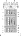
- FIG. 1 is a cross-sectional view illustrating an example of a capacitor element according to a first embodiment of the present invention.
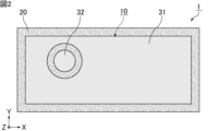
- FIG. 2 is a plan view taken along line AA of the capacitor element shown in FIG.
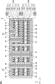
- FIG. 3 is a cross-sectional view illustrating an example of a capacitor element according to a second embodiment of the present invention.
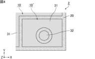
- FIG. 4 is a plan view of the capacitor element shown in FIG. 3 taken along line AA.
- FIG. 5 is a cross-sectional view that illustrates an example of a step of preparing an anode plate.
- FIG. 6 is a cross-sectional view that illustrates an example of a process for filling the inside of the porous portion with insulating resin.
- FIG. 1 is a cross-sectional view illustrating an example of a capacitor element according to a first embodiment of the present invention.
- FIG. 2 is a plan view taken along line AA of the capacitor element shown in FIG.
- FIG. 3 is a cross-sectional view illustrating an example
- FIG. 7 is a cross-sectional view illustrating an example of a process for forming a through hole.
- FIG. 8 is a cross-sectional view that illustrates an example of a process for forming an inner layer of a solid electrolyte layer.
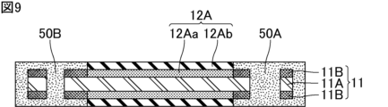
- FIG. 9 is a cross-sectional view that illustrates an example of a step of forming an outer layer of a solid electrolyte layer.
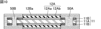
- FIG. 10 is a cross-sectional view that illustrates an example of a process for forming a carbon layer of a conductive layer.
- FIG. 11 is a cross-sectional view that illustrates an example of a process for forming a copper layer of a conductor layer.
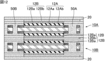
- FIG. 12 is a cross-sectional view that illustrates an example of a process for laminating the first capacitor layer and the second capacitor layer.
- FIG. 13 is a cross-sectional view illustrating an example of a step of forming the first through hole and the second through hole.
- FIG. 14 is a cross-sectional view illustrating an example of a process for forming a first through-hole conductor and a second through-hole conductor.
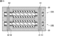
- FIG. 15 is a cross-sectional view illustrating an example of a process for forming the first resin filling portion and the second resin filling portion.
- 16A and 16B are cross-sectional views that diagrammatically show an example of a process for forming a first external electrode layer and a second external electrode layer.
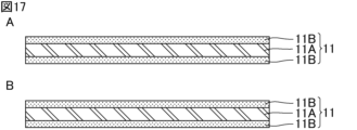
- 17A and 17B are cross-sectional views each showing a schematic example of a process for preparing an anode plate in a first capacitor tier and a second capacitor tier, respectively.
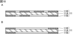
- 18A and 18B are cross-sectional views each showing an example of a process for filling a porous portion of a first capacitor layer with an insulating resin
- FIG. 18B is a cross-sectional view showing an example of a process for filling a porous portion of a second capacitor layer with an insulating resin.
- 19A and 19B are cross-sectional views each showing a schematic example of a process for forming a through groove and a through hole in a first capacitor layer and a second capacitor layer, respectively.
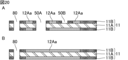
- 20A and 20B are cross-sectional views each showing a schematic example of a process for forming an inner layer of a solid electrolyte layer in a first capacitor layer and a second capacitor layer, respectively.
- 21A and 21B are cross-sectional views each showing a schematic example of a process for forming an outer layer of a solid electrolyte layer in a first capacitor layer and a second capacitor layer, respectively.
- 22A and 22B are cross-sectional views each showing a schematic example of a process for forming a carbon layer of a conductive layer in a first capacitor tier and a second capacitor tier, respectively.
- FIG. 23A and 23B are cross-sectional views each showing a schematic example of a process for forming a copper layer of a conductor layer in a first capacitor tier and a second capacitor tier, respectively.
- FIG. 24 is a cross-sectional view that illustrates an example of a process for laminating a first capacitor layer and a second capacitor layer.
- FIG. 25 is a cross-sectional view illustrating an example of a process for forming a via hole.
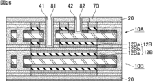
- FIG. 26 is a cross-sectional view illustrating an example of a process for forming a first through-hole conductor, a second through-hole conductor, and a via conductor.
- FIG. 24 is a cross-sectional view that illustrates an example of a process for laminating a first capacitor layer and a second capacitor layer.
- FIG. 25 is a cross-sectional view illustrating an example of a process for forming a via hole.
- FIG. 26 is a cross-sectional view illustrating an example of
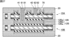
- 27 is a cross-sectional view illustrating an example of a process for forming the first resin filling portion and the second resin filling portion.
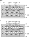
- 28A and 28B are cross-sectional views that diagrammatically show an example of a process for forming a first external electrode layer and a second external electrode layer.
- the capacitor element of the present invention is described below. Note that the present invention is not limited to the following configuration, and may be modified as appropriate without changing the gist of the present invention. In addition, a combination of multiple individual preferred configurations described below also constitutes the present invention.
- each embodiment will simply be referred to as the "capacitor element of the present invention.”
- terms indicating the relationship between elements e.g., "perpendicular,” “parallel,” “orthogonal,” etc.
- terms indicating the shapes of elements are not expressions that express only a strict meaning, but are expressions that include a range of substantial equivalence, for example, differences of about a few percent.
- Fig. 1 is a cross-sectional view showing an example of a capacitor element according to a first embodiment of the present invention
- Fig. 2 is a plan view taken along line AA of the capacitor element shown in Fig. 1.
- the capacitor element 1 shown in Figures 1 and 2 comprises a capacitor section 10 and a sealing layer 20 arranged to cover at least one of the main surfaces of the capacitor section 10.
- the capacitor section 10 includes a first capacitor layer 10A and a second capacitor layer 10B that face each other in the thickness direction (Z direction).
- one capacitor section 10 is disposed inside the sealing layer 20.
- the number of capacitor parts arranged inside the sealing layer 20 is not particularly limited, and may be one or more.
- multiple capacitor parts may be arranged in a planar direction (i.e., a planar direction parallel to the X-axis and Y-axis) perpendicular to the thickness direction (Z-direction).
- the sealing layer 20 is provided on both opposing main surfaces (top and bottom surfaces in FIG. 1) of the capacitor section 10 in the thickness direction.
- the sealing layer 20 protects the capacitor section 10.
- the sealing layer 20 may be composed of only one layer, or may be composed of two or more layers. When the sealing layer 20 is composed of two or more layers, the materials constituting each layer may be the same or different.
- the sealing layer 20 is formed to seal the capacitor section 10, for example, by a method of thermocompressing an insulating resin sheet, or by applying an insulating resin paste and then thermally curing it.
- the first capacitor layer 10A and the second capacitor layer 10B each include an anode plate 11 having a porous portion 11B on at least one main surface of a core portion 11A, a dielectric layer 13 provided on the surface of the porous portion 11B, and a cathode layer 12 provided on the surface of the dielectric layer 13.
- the anode plate 11 has a porous portion 11B on both main surfaces of the core portion 11A, but may have a porous portion 11B on only one of the main surfaces of the core portion 11A.
- the cathode layer 12 includes a solid electrolyte layer 12A provided on the surface of the dielectric layer 13, and a conductor layer 12B provided on the surface of the solid electrolyte layer 12A.
- the cathode layer 12 includes the solid electrolyte layer 12A, so that the capacitor section 10 constitutes a solid electrolytic capacitor.
- Examples of materials constituting the solid electrolyte layer 12A include conductive polymers such as poly(3,4-ethylenedioxythiophene) known as PEDOT.
- the conductive polymer may also contain a dopant such as polystyrene sulfonate (PSS).
- PSS polystyrene sulfonate
- the solid electrolyte layer 12A preferably includes an inner layer that fills the pores (recesses) of the dielectric layer 13, and an outer layer that covers the dielectric layer 13.
- the conductive layer 12B includes, for example, a carbon layer 12Ba provided on the surface of the solid electrolyte layer 12A and a copper layer 12Bb provided on the surface of the carbon layer 12Ba.
- the conductive layer 12B in the first capacitor layer 10A that faces the second capacitor layer 10B is the same as the conductive layer 12B in the second capacitor layer 10B that faces the first capacitor layer 10A. Note that if the conductive layer 12B is composed of two or more layers, it is sufficient that at least one of the layers is the same. In other words, it can be said that the first capacitor layer 10A and the second capacitor layer 10B share the same conductive layer 12B that is disposed between them.
- the copper layer 12Bb in the first capacitor layer 10A that faces the second capacitor layer 10B is the same as the copper layer 12Bb in the second capacitor layer 10B that faces the first capacitor layer 10A.
- the first capacitor layer 10A and the second capacitor layer 10B share the same copper layer 12Bb that is disposed between them.
- the capacitance per area of the capacitor section 10 can be increased. Furthermore, by making the conductive layer 12B in the first capacitor layer 10A that faces the second capacitor layer 10B the same as the conductive layer 12B in the second capacitor layer 10B that faces the first capacitor layer 10A, the thickness of the entire element can be reduced. Therefore, it is possible to achieve both large capacity and thinness.
- the element can be made of a material with high thermal conductivity without placing a thermal insulating material between the first capacitor layer 10A and the second capacitor layer 10B. This improves the heat dissipation properties of the element.
- the conductive layer 12B in the first capacitor layer 10A facing the second capacitor layer 10B is different from the conductive layer 12B in the second capacitor layer 10B facing the first capacitor layer 10A, wiring is required to electrically connect the first capacitor layer 10A and the second capacitor layer 10B, and the contact resistance increases.
- the conductive layer 12B in the first capacitor layer 10A facing the second capacitor layer 10B is the same as the conductive layer 12B in the second capacitor layer 10B facing the first capacitor layer 10A, there are fewer contacts with different materials and the series resistance component is smaller, so the equivalent series resistance (ESR) can be lowered.
- ESR equivalent series resistance
- the conductor layer 12B in the first capacitor layer 10A facing the second capacitor layer 10B is different from the conductor layer 12B in the second capacitor layer 10B facing the first capacitor layer 10A, wiring is required to electrically connect the first capacitor layer 10A and the second capacitor layer 10B, and the inductance component also increases.
- the conductor layer 12B in the first capacitor layer 10A facing the second capacitor layer 10B is the same as the conductor layer 12B in the second capacitor layer 10B facing the first capacitor layer 10A, the inductance component is smaller, and noise generation can be suppressed.
- the capacitor element 1 may further include a first external electrode layer 31 electrically connected to the cathode layer 12 of the first capacitor layer 10A and the cathode layer 12 of the second capacitor layer 10B.
- the first external electrode layer 31 is provided on at least one of the main surfaces of the sealing layer 20.
- the first external electrode layer 31 is provided on both main surfaces of the sealing layer 20 (top and bottom surfaces in FIG. 1), but it may be provided on either one of the main surfaces of the sealing layer 20 (top or bottom surface in FIG. 1).
- one first external electrode layer 31 may be provided, or multiple first external electrode layers 31 may be provided.
- the planar shape of the first external electrode layer 31 when viewed from the thickness direction is not particularly limited, and examples include a rectangle (square or oblong), a quadrangle other than a rectangle, a polygon such as a triangle, a pentagon, or a hexagon, a circle, an ellipse, or a combination of these.
- the planar shape of the first external electrode layer 31 may also be an L-shape, a C-shape, a stepped shape, etc.
- the capacitor element 1 may further include a second external electrode layer 32 electrically connected to the anode plate 11 of the first capacitor layer 10A and the anode plate 11 of the second capacitor layer 10B.
- the second external electrode layer 32 is provided on at least one of the main surfaces of the sealing layer 20.
- the second external electrode layer 32 is provided on both main surfaces of the sealing layer 20 (top and bottom surfaces in FIG. 1), but it may be provided on either one of the main surfaces of the sealing layer 20 (top or bottom surface in FIG. 1).
- one second external electrode layer 32 may be provided, or multiple second external electrode layers 32 may be provided.
- the number of second external electrode layers 32 may be the same as the number of first external electrode layers 31, or may be different.
- the planar shape of the second external electrode layer 32 when viewed from the thickness direction is not particularly limited, and examples include a rectangle (square or rectangle), a quadrangle other than a rectangle, a polygon such as a triangle, a pentagon, or a hexagon, a circle, an ellipse, or a combination of these.
- the planar shape of the second external electrode layer 32 may also be an L-shape, a C-shape, a stepped shape, or the like.
- the planar shape of the second external electrode layer 32 when viewed from the thickness direction may be the same as or different from the planar shape of the first external electrode layer 31 when viewed from the thickness direction.
- the first external electrode layer 31 is arranged so as to overlap at least a portion with the same conductor layer 12B (the same copper layer 12Bb shared by the first capacitor layer 10A and the second capacitor layer 10B in FIG. 1).
- the first external electrode layer 31 By arranging the first external electrode layer 31 so that at least a portion of it overlaps with the same conductor layer 12B, moisture is less likely to penetrate into the inside of the element. This makes it possible to suppress peeling, known as delamination, that occurs due to rapid evaporation of moisture.
- the permeation of moisture, oxygen, etc. into the inside of the element is suppressed, and deterioration of the conductive polymer contained in the solid electrolyte layer 12A can be suppressed.
- the area of the first external electrode layer 31 is increased, and a cathode layer 12 is also formed inside the element, thereby reducing the generation or emission of noise.
- the area of the portion where the first external electrode layer 31 overlaps with the same conductor layer 12B is large.
- the area of the first external electrode layer 31 provided on either one of the main surfaces of the sealing layer 20, which overlaps with the same conductor layer 12B is preferably 50% or more of the area of the same conductor layer 12B.
- the area of the first external electrode layer 31 provided on the upper surface of the sealing layer 20, which overlaps with the same conductor layer 12B may be 50% or more of the area of the same conductor layer 12B, or the area of the first external electrode layer 31 provided on the lower surface of the sealing layer 20, which overlaps with the same conductor layer 12B, may be 50% or more of the area of the same conductor layer 12B.
- the area of the first external electrode layer 31 provided on one of the main surfaces of the sealing layer 20 that overlaps with the same conductor layer 12B is not particularly limited in upper limit, as long as it is 100% or less of the area of the same conductor layer 12B.
- the above-mentioned area ratio may be the same or different between one main surface side and the other main surface side of the sealing layer 20. Therefore, even if the area of the first external electrode layer 31 provided on either one of the main surfaces of the sealing layer 20, which is a portion of the area of the first external electrode layer 31 that overlaps with the same conductor layer 12B, is 50% or more of the area of the same conductor layer 12B, the area of the first external electrode layer 31 provided on the other main surface of the sealing layer 20, which is a portion of the area of the first external electrode layer 31 that overlaps with the same conductor layer 12B may be less than 50% of the area of the same conductor layer 12B.
- the area of the first external electrode layer 31 that overlaps with the same conductor layer 12B is 50% or more of the area of the same conductor layer 12B, and, among the areas of the first external electrode layer 31 provided on the other main surface of the sealing layer 20, the area of the first external electrode layer 31 that overlaps with the same conductor layer 12B is 50% or more of the area of the same conductor layer 12B.
- the "total area of all the first external electrode layers 31 and second external electrode layers 32 provided on one of the main surfaces of the sealing layer 20" includes the area of the first external electrode layers 31 and second external electrode layers 32 that do not overlap with the same conductor layer 12B on the target main surface.
- the "area surrounded by the outer periphery of the sealing layer 20" does not mean the area of the sealing layer 20 itself, but the total area surrounded by the outer periphery of the sealing layer 20.
- the above-mentioned area ratios may be the same or different between one main surface side and the other main surface side of the sealing layer 20. Therefore, even if the total area of all the first external electrode layers 31 and second external electrode layers 32 provided on either one main surface of the sealing layer 20 is 50% or more of the area surrounded by the outer peripheral edge of the sealing layer 20, the total area of all the first external electrode layers 31 and second external electrode layers 32 provided on the other main surface of the sealing layer 20 may be less than 50% of the area surrounded by the outer peripheral edge of the sealing layer 20.
- the total area of all the first external electrode layers 31 and second external electrode layers 32 provided on one of the main surfaces of the sealing layer 20 is 50% or more of the area surrounded by the outer periphery of the sealing layer 20, and that the total area of all the first external electrode layers 31 and second external electrode layers 32 provided on the other main surface of the sealing layer 20 is 50% or more of the area surrounded by the outer periphery of the sealing layer 20.
- the capacitor element 1 may further include a first through-hole conductor 41 electrically connected to the first external electrode layer 31.
- the first through-hole conductor 41 only needs to be provided on at least the inner wall surface of the first through hole 51 that penetrates the capacitor section 10 and the sealing layer 20 in the thickness direction.
- the first through-hole conductor 41 may be provided only on the inner wall surface of the first through hole 51, or may be provided throughout the entire interior of the first through hole 51.
- one first through-hole conductor 41 may be provided inside the cathode layer 12, or two or more first through-hole conductors 41 may be provided.
- the end face of the anode plate 11 and the first through-hole conductor 41 are insulated by an insulating material.
- the first through-hole conductor 41 is preferably electrically connected to the cathode layer 12 of the first capacitor layer 10A and the cathode layer 12 of the second capacitor layer 10B on the inner wall surface of the first through hole 51.
- the capacitor element 1 may further include a second through-hole conductor 42 electrically connected to the second external electrode layer 32.
- the second through-hole conductor 42 may be provided at least on the inner wall surface of the second through hole 52 that penetrates the capacitor section 10 and the sealing layer 20 in the thickness direction.
- the second through-hole conductor 42 may be provided only on the inner wall surface of the second through hole 52, or may be provided throughout the entire interior of the second through hole 52.
- one second through-hole conductor 42 may be provided inside the cathode layer 12, or two or more second through-hole conductors 42 may be provided.
- the end face of the cathode layer 12 and the second through-hole conductor 42 are insulated from each other by an insulating material.
- the second through-hole conductor 42 is preferably electrically connected to the anode plate 11 of the first capacitor layer 10A and the anode plate 11 of the second capacitor layer 10B on the inner wall surface of the second through hole 52.
- a second resin filling portion 62 filled with a resin material may be provided inside the second through-hole conductor 42.
- the second resin filling portion 62 is provided in the space surrounded by the second through-hole conductor 42 in the second through hole 52.
- the second resin filling portion 62 may be a conductor or an insulator.
- the capacitor element 1 may further include a third through-hole conductor that is not electrically connected to the anode plate 11 and the cathode layer 12.
- the capacitor element 1 may further include a via conductor that is arranged to penetrate the sealing layer 20 in the thickness direction and has one end extended to the surface of the sealing layer 20.
- the capacitor element 1 may include a via conductor electrically connected to the anode plate 11.
- the anode plate 11 is electrically led out to the outside of the sealing layer 20 through the via conductor, and can be electrically connected to the outside of the sealing layer 20.
- the capacitor element 1 may include a via conductor electrically connected to the cathode layer 12.
- the cathode layer 12 is electrically led out to the outside of the sealing layer 20 through the via conductor, and can be electrically connected to the outside of the sealing layer 20.
- the capacitor section 10 may further include an insulating mask layer provided around the first through-hole conductor 41 or the second through-hole conductor 42 on at least one of the main surfaces of the anode plate 11.
- the capacitor section 10 may further include an insulating mask layer provided on at least one of the main surfaces of the anode plate 11 so as to surround the periphery of the cathode layer 12.
- an insulating mask layer provided on at least one of the main surfaces of the anode plate 11 so as to surround the periphery of the cathode layer 12.
- the areas of the capacitance parts of the first capacitor layer and the second capacitor layer are different.
- the areas of the capacitance parts of at least one capacitor part are different between the first capacitor layer and the second capacitor layer.
- FIG. 3 is a cross-sectional view showing a schematic example of a capacitor element according to a second embodiment of the present invention.
- FIG. 4 is a plan view of the capacitor element shown in FIG. 3 taken along line A-A.
- the sealing layer 20 is provided on both opposing main surfaces (top and bottom surfaces in FIG. 3) of the capacitor section 10 and the capacitor section 10' in the thickness direction.
- the sealing layer 20 protects the capacitor section 10 and the capacitor section 10'.
- the capacitor section 10 includes a first capacitor layer 10A and a second capacitor layer 10B that face each other in the thickness direction (Z direction).
- the capacitor section 10' includes a first capacitor layer 10A and a second capacitor layer 10B that face each other in the thickness direction (Z direction).
- the first capacitor layer 10A and the second capacitor layer 10B each include an anode plate 11 having a porous portion 11B on at least one main surface of the core portion 11A, a dielectric layer 13 provided on the surface of the porous portion 11B, and a cathode layer 12 provided on the surface of the dielectric layer 13.
- the anode plate 11 has a porous portion 11B on both main surfaces of the core portion 11A, but the anode plate 11 may have a porous portion 11B on only one of the main surfaces of the core portion 11A. The same is true for the capacitor section 10'.
- the cathode layer 12 includes a solid electrolyte layer 12A provided on the surface of the dielectric layer 13, and a conductor layer 12B provided on the surface of the solid electrolyte layer 12A. Since the cathode layer 12 includes the solid electrolyte layer 12A, the capacitor section 10 constitutes a solid electrolytic capacitor. The same is true for the capacitor section 10'.
- the conductive layer 12B in the first capacitor layer 10A that faces the second capacitor layer 10B is the same as the conductive layer 12B in the second capacitor layer 10B that faces the first capacitor layer 10A. Note that if the conductive layer 12B is composed of two or more layers, it is sufficient that at least one of the layers is the same. In other words, it can be said that the first capacitor layer 10A and the second capacitor layer 10B share the same conductive layer 12B that is disposed between them.
- the copper layer 12Bb in the first capacitor layer 10A that faces the second capacitor layer 10B is the same as the copper layer 12Bb in the second capacitor layer 10B that faces the first capacitor layer 10A.
- the first capacitor layer 10A and the second capacitor layer 10B share the same copper layer 12Bb that is disposed between them.
- the conductive layer 12B in the first capacitor layer 10A that faces the second capacitor layer 10B is the same as the conductive layer 12B in the second capacitor layer 10B that faces the first capacitor layer 10A.
- the conductive layer 12B is composed of two or more layers, it is sufficient that at least one of the layers is the same. In other words, it can be said that the first capacitor layer 10A and the second capacitor layer 10B share the same conductive layer 12B that is disposed between them.
- the copper layer 12Bb in the first capacitor layer 10A that faces the second capacitor layer 10B is the same as the copper layer 12Bb in the second capacitor layer 10B that faces the first capacitor layer 10A.
- the first capacitor layer 10A and the second capacitor layer 10B share the same copper layer 12Bb that is disposed between them.
- the area of the capacitance section differs between the first capacitor layer 10A and the second capacitor layer 10B.
- the areas of the capacitance sections of the first capacitor layer 10A and the second capacitor layer 10B may be the same or different.
- the number of capacitor parts arranged inside the sealing layer 20 is not particularly limited, and may be one or more.
- multiple capacitor parts may be arranged in a planar direction (i.e., a planar direction parallel to the X-axis and Y-axis) perpendicular to the thickness direction (Z-direction).
- the through groove 80 is filled with an insulating material such as a sealing layer 20.
- adjacent capacitor sections in the planar direction When adjacent capacitor sections in the planar direction are separated by a through groove 80, it is sufficient that adjacent capacitor sections 10 in the planar direction are physically separated by the through groove 80. Therefore, adjacent capacitor sections in the planar direction may be electrically separated or electrically connected.
- the width of the through groove 80 i.e., the distance between adjacent capacitor sections in the planar direction, may be constant in the thickness direction (Z direction) or may become smaller in the thickness direction.
- the capacitor parts When multiple capacitor parts are arranged in the planar direction, the capacitor parts may be arranged regularly or irregularly.
- the size and shape of the capacitor parts may be the same, or some or all of them may be different. It is preferable that the capacitor parts have the same configuration, but capacitor parts with different configurations may be included.
- the first capacitor layer 10A of the capacitor section 10' may be provided with a first through-hole conductor 41 that reaches the same conductor layer 12B.
- the first through-hole conductor 41 of the capacitor section 10' may be provided at least on the inner wall surface of the first via hole 81.
- the first through-hole conductor 41 may be provided only on the inner wall surface of the first via hole 81, or may be provided throughout the entire interior of the first via hole 81.
- one first through-hole conductor 41 may be provided inside the cathode layer 12 of the capacitor section 10', or two or more first through-hole conductors 41 may be provided.
- the end face of the anode plate 11 of the capacitor section 10' is insulated from the first through-hole conductor 41 by an insulating material.
- a first resin filling section 61 filled with a resin material may be provided on the inside of the first through-hole conductor 41.
- the first capacitor layer 10A of the capacitor section 10' may also be provided with a via conductor 70 that reaches the conductive layer 12B on the opposite side to the same conductive layer 12B.
- one via conductor 70 may be provided inside the cathode layer 12 of the capacitor section 10', or two or more via conductors 70 may be provided.
- first capacitor layer 10A of the capacitor section 10' may be provided with a second through-hole conductor 42 that reaches the core 11A of the anode plate 11.
- the second through-hole conductor 42 of the capacitor section 10' may be provided at least on the inner wall surface of the second via hole 82.
- the second through-hole conductor 42 may be provided only on the inner wall surface of the second via hole 82, or may be provided throughout the entire interior of the second via hole 82.
- one second through-hole conductor 42 may be provided inside the cathode layer 12 of the capacitor section 10', or two or more second through-hole conductors 42 may be provided.
- the end face of the cathode layer 12 of the capacitor section 10' and the second through-hole conductor 42 are insulated by an insulating material.
- a second resin filling section 62 filled with a resin material may be provided on the inside of the second through-hole conductor 42.
- Figure 5 is a cross-sectional view that shows a schematic example of a process for preparing an anode plate.
- an anode plate 11 made of a valve metal is prepared.
- an anodizing process is performed on an anode plate 11 having a porous portion 11B on both main surfaces of a core portion 11A, thereby forming a dielectric layer (not shown) on the surface of the porous portion 11B.
- a chemical foil may be prepared as the anode plate 11 with a dielectric layer (not shown) provided on the surface of the porous portion 11B.
- Figure 6 is a cross-sectional view that shows a schematic example of a process for filling the inside of a porous portion with insulating resin.
- an insulating resin such as polyimide resin is applied to a predetermined position on the top surface of the porous portion 11B, and the insulating resin is allowed to permeate into the interior of the porous portion 11B.
- Figure 7 is a cross-sectional view that shows a schematic example of a process for forming a through hole.
- a through hole 50A is formed by a laser or the like in the area where the first through-hole conductor is to be formed, and a through hole 50B is formed in the area where the second through-hole conductor is to be formed. As shown in FIG. 7, it is preferable that the diameter of the through hole 50A is larger than the diameter of the through hole 50B.
- Figure 8 is a cross-sectional view that shows a schematic example of a process for forming the inner layer of a solid electrolyte layer.
- a dispersion of PEDOT/PSS an example of a conductive polymer, is applied to the porous portion 11B surrounded by the insulating resin, allowed to penetrate, and then dried and solidified. This process is repeated until the porous portion 11B is filled with PEDOT/PSS. This forms the inner layer 12Aa of the solid electrolyte layer.
- Figure 9 is a cross-sectional view that shows a schematic example of a process for forming the outer layer of a solid electrolyte layer.
- a highly viscous PEDOT/PSS dispersion is applied and then dried and solidified. This forms the outer layer 12Ab of the solid electrolyte layer.
- the inner layer 12Aa and the outer layer 12Ab form the solid electrolyte layer 12A.
- insulating resin is applied to the surface of the insulating resin that has permeated the porous portion 11B, the inside of the through-hole 50A, and the inside of the through-hole 50B, and then solidified.
- FIG. 10 is a cross-sectional view that shows a schematic example of a process for forming a carbon layer of a conductive layer.
- a conductive resin containing carbon filler is applied to the surface of the solid electrolyte layer 12A and then solidified. This forms the carbon layer 12Ba.
- insulating resin is applied around the carbon layer 12Ba and allowed to harden.
- FIG. 11 is a cross-sectional view that shows a schematic example of a process for forming a copper layer of a conductive layer.
- a conductive resin containing copper filler is applied to the surface of the carbon layer 12Ba and solidified. This forms the copper layer 12Bb.
- the carbon layer 12Ba and the copper layer 12Bb form the conductor layer 12B.
- insulating resin is applied around the copper layer 12Bb and allowed to solidify. At this time, it is preferable to adjust the height so that the copper layer 12Bb and the insulating resin are as flat as possible.
- FIG. 12 is a cross-sectional view that shows a schematic example of a process for stacking a first capacitor layer and a second capacitor layer.
- the first capacitor layer 10A and the second capacitor layer 10B are stacked together with the front and back conductive layers 12B.
- an insulating resin sheet such as Ajinomoto Build-up Film (ABF) is laminated on the surface of the laminate. After lamination, the laminate is placed in a mold and vacuum degassed, and then thermocompressed and cured. This forms the sealing layer 20.
- ABSF Ajinomoto Build-up Film
- FIG. 13 is a cross-sectional view that shows a schematic example of a process for forming a first through hole and a second through hole.
- a first through hole 51 with a diameter of about 100 ⁇ m is formed at a predetermined position where the insulating resin has been formed using a laser such as a UV laser.
- the copper layer 12Bb is exposed on the side of the first through hole 51.
- a second through hole 52 with a diameter of about 100 ⁇ m is formed at a predetermined position where the insulating resin has been formed using a laser such as a UV laser.
- the anode plate 11 is exposed on the side of the second through hole 52.
- FIG. 14 is a cross-sectional view that shows a schematic example of a process for forming a first through-hole conductor and a second through-hole conductor.
- the inner surface of the first through hole 51 is subjected to, for example, electroless copper plating. Then, electrolytic copper plating is performed. This forms the first through-hole conductor 41.
- the second through hole 52 is subjected to, for example, a zincate treatment, followed by nickel plating and electroless copper plating. Then, electrolytic copper plating is performed. This forms the second through-hole conductor 42.
- FIG. 15 is a cross-sectional view that shows a schematic example of a process for forming a first resin-filled portion and a second resin-filled portion.
- a first resin-filled portion 61 is formed by filling the first through hole 51 in which the first through-hole conductor 41 is formed with insulating resin
- a second resin-filled portion 62 is formed by filling the second through hole 52 in which the second through-hole conductor 42 is formed with insulating resin.
- FIGS. 16A and 16B are cross-sectional views that show a schematic example of a process for forming a first external electrode layer and a second external electrode layer.
- the surface of the sealing layer 20 is subjected to, for example, electrolytic copper plating to form a plating layer 30.
- the plating layer 30 is etched so as to separate the cathode portion and the anode portion, thereby forming a first external electrode layer 31 and a second external electrode layer 32.
- the copper layer 12Bb may be formed on the entire surface except for the area where the second through holes 52 are formed.
- the outer periphery and the inner conductive layer 12B can be connected with a single through-hole conductor.
- the second capacitor layer 10B of the capacitor section 10' does not appear to be functional in FIG. 3, by forming via conductors or through-hole conductors similar to those in the first capacitor layer 10A, it is possible to form a capacitor of a different size from the first capacitor layer 10A, or to form a second capacitor layer 10B independent of the first capacitor layer 10A.
- FIG. 17A is a cross-sectional view showing a schematic example of a process for preparing an anode plate in a first capacitor layer.
- FIG. 17B is a cross-sectional view showing a schematic example of a process for preparing an anode plate in a second capacitor layer.
- an anode plate 11 made of a valve metal is prepared, similar to the process shown in Figure 5.
- FIG. 18A is a cross-sectional view showing an example of a process for filling an insulating resin inside a porous portion in a first capacitor layer.
- FIG. 18B is a cross-sectional view showing an example of a process for filling an insulating resin inside a porous portion in a second capacitor layer.
- an insulating resin such as polyimide resin is applied to a predetermined position on the upper surface of the porous portion 11B, and the insulating resin is allowed to permeate into the interior of the porous portion 11B.
- FIG. 19A is a cross-sectional view showing an example of a process for forming a through groove and a through hole in a first capacitor layer.
- FIG. 19B is a cross-sectional view showing an example of a process for forming a through groove in a second capacitor layer.
- a through groove 80 is formed by using a laser or the like to separate the capacitor part 10 and the capacitor part 10'.
- a through hole 50A is formed by a laser or the like in the portion where the first through-hole conductor is to be formed, and a through hole 50B is formed in the portion where the second through-hole conductor is to be formed.
- the diameter of the through hole 50A is larger than the diameter of the through hole 50B.
- the through hole 50B shown in FIG. 19 etc. does not penetrate the anode plate 11, it is referred to as a "through hole" for convenience.
- FIG. 20A is a cross-sectional view showing an example of a process for forming an inner layer of a solid electrolyte layer in a first capacitor layer.
- FIG. 20B is a cross-sectional view showing an example of a process for forming an inner layer of a solid electrolyte layer in a second capacitor layer.
- the inner layer 12Aa of the solid electrolyte layer is formed, similar to the process shown in Figure 8.
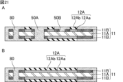
- FIG. 21A is a cross-sectional view showing an example of a process for forming an outer layer of a solid electrolyte layer in a first capacitor layer.
- FIG. 21B is a cross-sectional view showing an example of a process for forming an outer layer of a solid electrolyte layer in a second capacitor layer.
- the outer layer 12Ab of the solid electrolyte layer is formed, similar to the process shown in FIG. 9.
- the inner layer 12Aa and the outer layer 12Ab form the solid electrolyte layer 12A.
- insulating resin is applied to the surface of the insulating resin that has permeated the porous portion 11B, the inside of the through groove 80, the inside of the through hole 50A, and the inside of the through hole 50B, and then solidified.
- FIG. 22A is a cross-sectional view showing an example of a process for forming a carbon layer of a conductive layer in a first capacitor layer.
- FIG. 22B is a cross-sectional view showing an example of a process for forming a carbon layer of a conductive layer in a second capacitor layer.
- a carbon layer 12Ba is formed, similar to the process shown in Figure 10.
- an insulating resin is applied around the carbon layer 12Ba and allowed to harden.
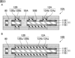
- FIG. 23A is a cross-sectional view showing an example of a process for forming a copper layer of a conductor layer in a first capacitor layer.
- FIG. 23B is a cross-sectional view showing an example of a process for forming a copper layer of a conductor layer in a second capacitor layer.
- a copper layer 12Bb is formed, similar to the process shown in Figure 11.
- the carbon layer 12Ba and the copper layer 12Bb form the conductor layer 12B.
- insulating resin is applied around the copper layer 12Bb and allowed to solidify. At this time, it is preferable to adjust the height so that the copper layer 12Bb and the insulating resin are as flat as possible.
- the substrate having the configuration shown in FIG. 23A constitutes the first capacitor layer 10A, and the substrate having the configuration shown in FIG. 23B constitutes the second capacitor layer 10B.
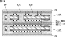
- Figure 24 is a cross-sectional view that shows a schematic example of a process for stacking a first capacitor layer and a second capacitor layer.
- the first capacitor layer 10A and the second capacitor layer 10B are stacked together to match the front and back conductive layers 12B.
- an insulating resin sheet such as Ajinomoto Build-up Film (ABF) is laminated on the surface of the laminate. After lamination, the laminate is placed in a mold and vacuum degassed, and then thermocompressed and cured. This forms the sealing layer 20.
- ABSF Ajinomoto Build-up Film
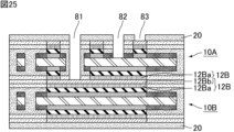
- Figure 25 is a cross-sectional view that shows a schematic example of a process for forming a via hole.
- the laser output is adjusted to form a first via hole 81 at a predetermined position where the insulating resin has been formed, up to the center of the substrate where the conductive layer 12B is exposed.
- the laser output is adjusted to form a second via hole 82 up to the part where the core 11A of the anode plate 11 is exposed.
- a third via hole 83 is also formed that does not penetrate the conductive layer 12B on the front side of the substrate.
- FIG. 26 is a cross-sectional view that shows a schematic example of a process for forming a first through-hole conductor, a second through-hole conductor, and a via conductor.
- the inner surface of the first via hole 81 is subjected to, for example, electroless copper plating. Then, electrolytic copper plating is performed. This forms the first through-hole conductor 41.
- the second via hole 82 is subjected to, for example, a zincate treatment, followed by nickel plating and electroless copper plating. Then, electrolytic copper plating is performed. This forms the second through-hole conductor 42.
- electroless copper plating is performed on the third via hole 83, and then electrolytic copper plating is performed. This forms the via conductor 70.
- FIG. 27 is a cross-sectional view that shows a schematic example of a process for forming a first resin-filled portion and a second resin-filled portion.
- a first resin-filled portion 61 is formed by filling a first via hole 81 in which a first through-hole conductor 41 is formed with insulating resin
- a second resin-filled portion 62 is formed by filling a second via hole 82 in which a second through-hole conductor 42 is formed with insulating resin.
- 28A and 28B are cross-sectional views that show a schematic example of a process for forming a first external electrode layer and a second external electrode layer.
- the surface of the sealing layer 20 is subjected to, for example, electrolytic copper plating to form a plating layer 30.
- the plating layer 30 is etched so as to separate the cathode portion and the anode portion, thereby forming a first external electrode layer 31 and a second external electrode layer 32.
- the capacitor section it is preferable to process the capacitor section so that it is not completely separated, for example by cutting it in the X direction and filling it with resin, and then cutting it in the Y direction and filling it with resin.
- capacitor elements 1 and 2 The detailed configuration of capacitor elements 1 and 2 is described below.
- the planar shape of the capacitor section 10 when viewed from the thickness direction may be, for example, a rectangle (square or oblong), a quadrangle other than a rectangle, a polygon such as a triangle, a pentagon, or a hexagon, a circle, an ellipse, or a combination of these.
- the planar shape of the capacitor section 10 may also be an L-shape, a C-shape, a stepped shape, or the like. The same applies below to the capacitor section 10'.
- the anode plate 11 is preferably made of a valve metal that exhibits so-called valve action.
- valve metals include simple metals such as aluminum, tantalum, niobium, titanium, and zirconium, or alloys containing at least one of these metals. Of these, aluminum or an aluminum alloy is preferred.
- the shape of the anode plate 11 is preferably flat, and more preferably foil-like.
- plate-like includes “foil-like”.
- the anode plate 11 may have a porous portion 11B on at least one of the main surfaces of the core portion 11A.
- the anode plate 11 may have a porous portion 11B on only one of the main surfaces of the core portion 11A, or may have a porous portion 11B on both main surfaces of the core portion 11A.
- the porous portion 11B is preferably a porous layer formed on the surface of the core portion 11A, and is more preferably an etched layer.
- the thickness of the anode plate 11 before the etching process is preferably 60 ⁇ m or more and 200 ⁇ m or less.
- the thickness of the unetched core portion 11A after the etching process is preferably 15 ⁇ m or more and 70 ⁇ m or less.
- the thickness of the porous portion 11B is designed according to the required withstand voltage and electrostatic capacitance, but it is preferably 10 ⁇ m or more and 180 ⁇ m or less when including the porous portions 11B on both sides of the core portion 11A.
- the pore diameter of the porous portion 11B is preferably 10 nm or more and 600 nm or less.
- the pore diameter of the porous portion 11B means the median diameter D50 measured by a mercury porosimeter.
- the pore diameter of the porous portion 11B can be controlled, for example, by adjusting various etching conditions.
- the dielectric layer 13 provided on the surface of the porous portion 11B is porous, reflecting the surface condition of the porous portion 11B, and has a finely uneven surface shape.
- the dielectric layer 13 is preferably made of an oxide film of the valve metal.
- the dielectric layer 13 made of an oxide film can be formed by anodizing the surface of the aluminum foil in an aqueous solution containing ammonium adipate or the like (also called chemical conversion treatment).
- the thickness of the dielectric layer 13 is designed according to the required withstand voltage and capacitance, but is preferably 10 nm or more and 100 nm or less.
- Materials constituting the solid electrolyte layer 12A contained in the cathode layer 12 include, for example, conductive polymers such as polypyrroles, polythiophenes, and polyanilines. Among these, polythiophenes are preferred, and poly(3,4-ethylenedioxythiophene), also known as PEDOT, is particularly preferred.
- the conductive polymer may also contain a dopant such as polystyrene sulfonate (PSS).
- PSS polystyrene sulfonate
- the solid electrolyte layer 12A preferably includes an inner layer that fills the pores (recesses) of the dielectric layer 13, and an outer layer that covers the dielectric layer 13.
- the thickness of the solid electrolyte layer 12A from the surface of the porous portion 11B is preferably 2 ⁇ m or more and 20 ⁇ m or less.
- the solid electrolyte layer 12A is formed, for example, by a method of forming a polymerized film of poly(3,4-ethylenedioxythiophene) or the like on the surface of the dielectric layer 13 using a treatment liquid containing a monomer such as 3,4-ethylenedioxythiophene, or by applying a dispersion of a polymer such as poly(3,4-ethylenedioxythiophene) to the surface of the dielectric layer 13 and drying it.
- the solid electrolyte layer 12A can be formed in a predetermined area by applying the above-mentioned treatment liquid or dispersion liquid to the surface of the dielectric layer 13 by a method such as sponge transfer, screen printing, dispenser application, or inkjet printing.
- the conductor layer 12B includes at least one of a conductive resin layer and a metal layer.
- the conductor layer 12B may be only a conductive resin layer or only a metal layer. It is preferable that the conductor layer 12B covers the entire surface of the solid electrolyte layer 12A.
- the conductive resin layer may be, for example, a conductive adhesive layer containing at least one conductive filler selected from the group consisting of silver filler, copper filler, nickel filler, and carbon filler.
- the metal layer examples include metal plating films and metal foils.
- the metal layer is preferably made of at least one metal selected from the group consisting of nickel, copper, silver, and alloys containing these metals as the main components.
- the term "main component" refers to the elemental component with the largest weight ratio.
- the conductive layer 12B includes, for example, a carbon layer provided on the surface of the solid electrolyte layer 12A and a copper layer provided on the surface of the carbon layer.
- the carbon layer is provided to electrically and mechanically connect the solid electrolyte layer 12A and the copper layer.
- the carbon layer can be formed in a predetermined area by applying carbon paste to the surface of the solid electrolyte layer 12A by sponge transfer, screen printing, dispenser application, inkjet printing, or other methods.
- the thickness of the carbon layer is preferably 2 ⁇ m or more and 20 ⁇ m or less.
- the copper layer can be formed in a predetermined area by applying copper paste to the surface of the carbon layer by sponge transfer, screen printing, spray application, dispenser application, inkjet printing, or other methods.
- the thickness of the copper layer is preferably 2 ⁇ m or more and 20 ⁇ m or less.
- the sealing layer 20 preferably contains an insulating resin.
- the sealing layer 20 further contains an inorganic filler.
- inorganic fillers contained in the sealing layer 20 include silica particles, alumina particles, etc.
- a layer such as a stress relief layer or a moisture-proof film may be provided.
- An insulating mask layer may be provided around the first through-hole conductor 41 or the second through-hole conductor 42 on at least one of the main surfaces of the anode plate 11. Also, an insulating mask layer may be provided around the cathode layer 12 on at least one of the main surfaces of the anode plate 11.
- the insulating mask layer is made of an insulating material. In this case, it is preferable that the insulating mask layer is made of an insulating resin.
- Examples of insulating resins constituting the insulating mask layer include polyphenylsulfone resin, polyethersulfone resin, cyanate ester resin, fluororesin (tetrafluoroethylene, tetrafluoroethylene-perfluoroalkylvinylether copolymer, etc.), polyimide resin, polyamideimide resin, epoxy resin, and derivatives or precursors thereof.
- the insulating mask layer may be made of the same resin as the sealing layer 20. Unlike the sealing layer 20, if the insulating mask layer contains inorganic filler, this may adversely affect the effective capacitance portion of the capacitor section 10, so it is preferable that the insulating mask layer is made of a resin alone.
- the insulating mask layer can be formed in a predetermined area by applying a mask material, such as a composition containing an insulating resin, to the surface of the porous portion 11B by a method such as sponge transfer, screen printing, dispenser application, or inkjet printing.
- a mask material such as a composition containing an insulating resin
- the insulating mask layer may be formed on the porous portion 11B either before the dielectric layer 13 is formed or after the dielectric layer 13 is formed.
- the first external electrode layer 31 is electrically connected to the cathode layer 12.
- the first external electrode layer 31 is provided on the surface of the first through-hole conductor 41, and functions as a connection terminal of the capacitor section 10.
- the constituent material of the first external electrode layer 31 may be, for example, a metal material containing a low-resistance metal such as silver, gold, or copper.
- the first external electrode layer 31 is formed, for example, by plating the surface of the first through-hole conductor 41.
- a mixed material of at least one conductive filler selected from the group consisting of silver filler, copper filler, nickel filler, and carbon filler, and resin may be used as the constituent material of the first external electrode layer 31.
- the second external electrode layer 32 is electrically connected to the anode plate 11.
- the second external electrode layer 32 is provided on the surface of the second through-hole conductor 42, and functions as a connection terminal for the capacitor section 10.
- the second external electrode layer 32 is electrically connected to the anode plate 11 via the second through-hole conductor 42, and functions as a connection terminal for the anode plate 11.
- the second external electrode layer 32 may be made of a metal material containing a low-resistance metal such as silver, gold, or copper.
- the second external electrode layer 32 is formed by, for example, plating the surface of the second through-hole conductor 42.
- a mixed material of at least one conductive filler selected from the group consisting of silver filler, copper filler, nickel filler, and carbon filler and resin may be used as the constituent material of the second external electrode layer 32.
- the constituent materials of the first external electrode layer 31 and the second external electrode layer 32 are preferably the same as each other at least in terms of type, but may be different from each other.
- each capacitor section When multiple capacitor sections are arranged in the planar direction, each capacitor section may be provided with a first external electrode layer 31 electrically connected to the cathode layer 12 and a second external electrode layer 32 electrically connected to the anode plate 11, and at least one of the first external electrode layer 31 and the second external electrode layer 32 may be provided in common among the multiple capacitor sections.
- the first external electrode layer 31 may be provided on both main surfaces of the sealing layer 20, or may be provided on only one main surface of the sealing layer 20.
- the second external electrode layer 32 may be provided on both main surfaces of the sealing layer 20, or may be provided on only one main surface of the sealing layer 20.
- the first external electrode layer 31 and the second external electrode layer 32 may be provided on the same main surface of the sealing layer 20, or may be provided on different main surfaces.
- one of the first external electrode layer 31 and the second external electrode layer 32 may be provided on both main surfaces of the sealing layer 20, and the other may be provided on only one main surface of the sealing layer 20.
- the first through-hole conductor 41 When the first through-hole conductor 41 is electrically connected to the cathode layer 12 on the inner wall surface of the first through hole 51, it is preferable that the first through-hole conductor 41 is electrically connected to the end surface of the conductive layer 12B that faces the inner wall surface of the first through hole 51 in the planar direction. As a result, the cathode layer 12 is electrically led out to the outside via the first through-hole conductor 41.
- the first through-hole conductor 41 is electrically connected to the conductive layer 12B around the entire circumference of the first through hole 51.
- the connection resistance between the conductive layer 12B and the first through-hole conductor 41 tends to decrease, and therefore the equivalent series resistance (ESR) tends to decrease.
- the second through-hole conductor 42 is electrically connected to the anode plate 11 on the inner wall surface of the second through hole 52, it is preferable that the second through-hole conductor 42 is electrically connected to the end surface of the anode plate 11 that faces the inner wall surface of the second through hole 52 in the surface direction. As a result, the anode plate 11 is electrically led out to the outside via the second through-hole conductor 42.
- the core portion 11A and the porous portion 11B are exposed on the end face of the anode plate 11 that is electrically connected to the second through-hole conductor 42.
- the porous portion 11B as well as the core portion 11A are electrically connected to the second through-hole conductor 42.
- the second through-hole conductor 42 is electrically connected to the anode plate 11 around the entire circumference of the second through hole 52.
- the connection resistance between the anode plate 11 and the second through-hole conductor 42 tends to decrease, and therefore the equivalent series resistance (ESR) tends to decrease.
- the first through-hole conductor 41 is formed, for example, as follows. First, a through hole penetrating the capacitor section 10 in the thickness direction is formed by drilling, laser processing, etc. Next, the above-mentioned through hole is filled with an insulating material. The part filled with the insulating material is drilled, laser processing, etc. to form the first through hole 51. At this time, the diameter of the first through hole 51 is made smaller than the diameter of the through hole filled with the insulating material, so that the insulating material is present between the inner wall surface of the previously formed through hole and the inner wall surface of the first through hole 51 in the surface direction.
- the inner wall surface of the first through hole 51 is metallized with a metal material containing a low-resistance metal such as copper, gold, or silver, thereby forming the first through-hole conductor 41.
- a metal material containing a low-resistance metal such as copper, gold, or silver
- the inner wall surface of the first through hole 51 can be metallized with electroless copper plating, electrolytic copper plating, etc., to facilitate processing.
- the method of forming the first through-hole conductor 41 may be a method of filling the first through-hole 51 with a metal material, a composite material of metal and resin, or the like, in addition to a method of metallizing the inner wall surface of the first through-hole 51.
- the second through-hole conductor 42 is formed, for example, as follows. First, the second through-hole 52 is formed by drilling, laser processing, or the like, penetrating the capacitor section 10 and the sealing layer 20 in the thickness direction. Then, the inner wall surface of the second through-hole 52 is metallized with a metal material containing a low-resistance metal such as copper, gold, or silver, to form the second through-hole conductor 42. When forming the second through-hole conductor 42, for example, the inner wall surface of the second through-hole 52 is metallized with an electroless copper plating process, an electrolytic copper plating process, or the like, to facilitate processing.
- a metal material containing a low-resistance metal such as copper, gold, or silver
- the method of forming the second through-hole conductor 42 may be a method of filling the second through-hole 52 with a metal material, a composite material of metal and resin, or the like, in addition to a method of metallizing the inner wall surface of the second through-hole 52.
- An anode connection layer may be provided between the anode plate 11 and the second through-hole conductor 42 in the planar direction.
- the anode plate 11 and the second through-hole conductor 42 may be electrically connected via the anode connection layer.
- the anode connection layer functions as a barrier layer for the anode plate 11, more specifically, as a barrier layer for the core portion 11A and the porous portion 11B.
- the anode connection layer functions as a barrier layer for the anode plate 11
- dissolution of the anode plate 11 that occurs during chemical treatment to form external electrode layers such as the second external electrode layer 32 is suppressed, and thus the infiltration of the chemical solution into the capacitor portion 10 is suppressed, which tends to improve reliability.
- the anode connection layer preferably includes a layer mainly composed of nickel. In this case, damage to the metal (e.g., aluminum) constituting the anode plate 11 is reduced, and the barrier properties of the anode connection layer against the anode plate 11 are easily improved.
- the metal e.g., aluminum
- an anode connection layer does not have to be provided between the anode plate 11 and the second through-hole conductor 42 in the surface direction.
- the second through-hole conductor 42 may be directly connected to the end surface of the anode plate 11.
- Examples of materials that can be used to form the via conductors 70 include metal materials that contain low-resistance metals such as silver, gold, and copper.
- the via conductor 70 is formed, for example, by plating the inner wall surface of a via hole that penetrates the sealing layer 20 in the thickness direction with the metal material described above, or by filling it with a conductive paste and then performing a heat treatment.
- the capacitor element of the present invention is not limited to the above embodiment, and various applications and modifications can be made within the scope of the present invention with respect to the configuration of the capacitor element, manufacturing conditions, etc.
- the conductive layer in the first capacitor layer that faces the second capacitor layer may be the same as the conductive layer in the second capacitor layer that faces the first capacitor layer.
- the capacitor section may include three or more capacitor layers.
- the capacitor section may further include a third capacitor layer that faces the first capacitor layer in the thickness direction on the side opposite the second capacitor layer.
- the conductive layer in the first capacitor layer that faces the third capacitor layer is the same as the conductive layer in the third capacitor layer that faces the first capacitor layer.
- the capacitor section may further include a fourth capacitor layer that faces the second capacitor layer in the thickness direction on the side opposite the first capacitor layer. In this case, it is preferable that the conductive layer in the second capacitor layer that faces the fourth capacitor layer is the same as the conductive layer in the fourth capacitor layer that faces the second capacitor layer.
- a capacitor section that includes only one of the first capacitor layer and the second capacitor layer may be included.
- the capacitor element of the present invention can be suitably used as a constituent material of a composite electronic component.
- a composite electronic component includes, for example, the capacitor element of the present invention, an external electrode layer provided on the surface of the sealing layer of the capacitor element and electrically connected to each of the anode plate and cathode layer of the capacitor element, and an electronic component connected to the external electrode layer.
- the electronic component connected to the external electrode layer may be a passive element or an active element. Both the passive element and the active element may be connected to the external electrode layer, or either the passive element or the active element may be connected to the external electrode layer. Also, a composite of a passive element and an active element may be connected to the external electrode layer.
- Passive elements include, for example, inductors. Active elements include memory, GPUs (Graphical Processing Units), CPUs (Central Processing Units), MPUs (Micro Processing Units), PMICs (Power Management ICs), etc.
- the capacitor element of the present invention has a sheet-like shape overall. Therefore, in a composite electronic component, the capacitor element can be treated like a mounting board, and electronic components can be mounted on the capacitor element. Furthermore, by making the electronic components to be mounted on the capacitor element into a sheet-like shape, it is also possible to connect the capacitor element and the electronic components in the thickness direction via through-hole conductors that penetrate each electronic component in the thickness direction. As a result, the active elements and passive elements can be configured like a single module.
- a switching regulator can be formed by electrically connecting the capacitor element of the present invention between a voltage regulator including a semiconductor active element and a load to which the converted DC voltage is supplied.
- a circuit layer may be formed on one side of a capacitor matrix sheet on which a plurality of capacitor elements of the present invention are laid out, and the capacitor elements may then be connected to passive or active elements.
- the capacitor element of the present invention may be placed in a cavity portion previously provided in a substrate, embedded in resin, and then a circuit layer may be formed on the resin.
- Another electronic component passive element or active element
- the capacitor element of the present invention may be mounted on a smooth carrier such as a wafer or glass, an outer layer made of resin may be formed, a circuit layer may be formed, and then the capacitor element may be connected to a passive or active element.
- a capacitor section including a first capacitor layer and a second capacitor layer opposed to each other in a thickness direction; a sealing layer provided so as to cover at least one main surface of the capacitor portion, each of the first capacitor layer and the second capacitor layer includes an anode plate having a porous portion on at least one main surface of a core portion, a dielectric layer provided on a surface of the porous portion, and a cathode layer provided on a surface of the dielectric layer; the cathode layer includes a solid electrolyte layer provided on a surface of the dielectric layer and a conductor layer provided on the surface of the solid electrolyte layer, A capacitor element, wherein the conductive layer in the first capacitor layer facing the second capacitor layer is the same as the conductive layer in the second capacitor layer facing the first capacitor layer.
- ⁇ 2> a first external electrode layer provided on at least one main surface of the sealing layer so as to be electrically connected to the cathode layer of the first capacitor layer and the cathode layer of the second capacitor layer;
- a capacitor element described in ⁇ 2> wherein, when viewed in a plane from the thickness direction, the area of the first external electrode layer provided on either one of the main surfaces of the sealing layer, of a portion of the first external electrode layer that overlaps with the same conductive layer, is 50% or more of the area of the same conductive layer.
- ⁇ 4> a first through-hole conductor provided on at least an inner wall surface of a first through hole penetrating the capacitor portion and the sealing layer in the thickness direction, the first through-hole conductor being electrically connected to the first external electrode layer,
- ⁇ 5> a first external electrode layer provided on at least one main surface of the sealing layer so as to be electrically connected to the cathode layer of the first capacitor layer and the cathode layer of the second capacitor layer; a second external electrode layer provided on at least one main surface of the sealing layer so as to be electrically connected to the anode plate of the first capacitor layer and the anode plate of the second capacitor layer;
- ⁇ 6> A capacitor element described in ⁇ 5>, wherein, when viewed in a plane from the thickness direction, the total area of all of the first external electrode layers and the second external electrode layers provided on either one of the main surfaces of the sealing layer is 50% or more of the area surrounded by the outer peripheral edge of the sealing layer.
- ⁇ 7> a first through-hole conductor provided on at least an inner wall surface of a first through hole penetrating the capacitor portion and the sealing layer in the thickness direction, the first through-hole conductor being electrically connected to the first external electrode layer; a second through-hole conductor provided on at least an inner wall surface of a second through hole penetrating the capacitor portion and the sealing layer in the thickness direction, the second through-hole conductor being electrically connected to the second external electrode layer, the first through-hole conductor is electrically connected to the cathode layer of the first capacitor layer and the cathode layer of the second capacitor layer on an inner wall surface of the first through hole;
- ⁇ 8> The capacitor element according to any one of ⁇ 1> to ⁇ 7>, wherein the first capacitor layer and the second capacitor layer have different areas of capacitance parts.
Landscapes
- Engineering & Computer Science (AREA)
- Power Engineering (AREA)
- Microelectronics & Electronic Packaging (AREA)
- Fixed Capacitors And Capacitor Manufacturing Machines (AREA)
Abstract
Description
本発明は、コンデンサ素子に関する。 The present invention relates to a capacitor element.
特許文献1には、1枚の固体電解コンデンサシートが分割されてなる複数の固体電解コンデンサ素子と、シート状の第1封止層と、シート状の第2封止層とを備えるコンデンサアレイが開示されている。上記固体電解コンデンサシートは、弁作用金属からなる陽極板と、上記陽極板の少なくとも一方の主面に設けられた多孔質層と、上記多孔質層の表面に設けられた誘電体層と、上記誘電体層の表面に設けられた固体電解質層を含む陰極層とを備え、厚み方向に相対する第1主面及び第2主面を有する。上記複数の固体電解コンデンサ素子は、それぞれの上記第1主面側が上記第1封止層上に配置されている。上記第2封止層は、上記第1封止層上の上記複数の固体電解コンデンサ素子を上記第2主面側から覆うように配置されている。上記固体電解コンデンサ素子間はスリット状のシート除去部によって分割されている。 Patent Document 1 discloses a capacitor array including a plurality of solid electrolytic capacitor elements formed by dividing a single solid electrolytic capacitor sheet, a sheet-like first sealing layer, and a sheet-like second sealing layer. The solid electrolytic capacitor sheet includes an anode plate made of a valve metal, a porous layer provided on at least one main surface of the anode plate, a dielectric layer provided on the surface of the porous layer, and a cathode layer including a solid electrolyte layer provided on the surface of the dielectric layer, and has a first main surface and a second main surface opposed in the thickness direction. The first main surface side of each of the plurality of solid electrolytic capacitor elements is disposed on the first sealing layer. The second sealing layer is disposed so as to cover the plurality of solid electrolytic capacitor elements on the first sealing layer from the second main surface side. The solid electrolytic capacitor elements are divided by a slit-shaped sheet removal portion.
特許文献1に記載されているようなコンデンサアレイにおいては、従来以上の大容量及び薄型化の両立が求められている。 In capacitor arrays such as those described in Patent Document 1, there is a demand for greater capacity and thinner dimensions than ever before.
なお、上記の問題は、面方向に複数個のコンデンサ部が配置されている構造に限らず、面方向に1個のコンデンサ部が配置されている構造にも生じる問題である。 Note that the above problem is not limited to structures in which multiple capacitor parts are arranged in the plane direction, but also occurs in structures in which one capacitor part is arranged in the plane direction.
本発明は、上記の問題を解決するためになされたものであり、大容量及び薄型化の両立が可能なコンデンサ素子を提供することを目的とする。 The present invention was made to solve the above problems, and aims to provide a capacitor element that is both large capacity and thin.
本発明のコンデンサ素子は、厚さ方向に対向する第1コンデンサ層及び第2コンデンサ層を含むコンデンサ部と、上記コンデンサ部の少なくとも一方の主面を覆うように設けられた封止層と、を備える。上記第1コンデンサ層及び上記第2コンデンサ層は、各々、芯部の少なくとも一方の主面に多孔質部を有する陽極板と、上記多孔質部の表面に設けられた誘電体層と、上記誘電体層の表面に設けられた陰極層と、を含む。上記陰極層は、上記誘電体層の表面に設けられた固体電解質層と、上記固体電解質層の表面に設けられた導電体層と、を含む。上記第1コンデンサ層中の、上記第2コンデンサ層と対向する上記導電体層は、上記第2コンデンサ層中の、上記第1コンデンサ層と対向する上記導電体層と同一である。 The capacitor element of the present invention comprises a capacitor section including a first capacitor layer and a second capacitor layer opposed to each other in the thickness direction, and a sealing layer provided to cover at least one main surface of the capacitor section. The first capacitor layer and the second capacitor layer each include an anode plate having a porous portion on at least one main surface of a core portion, a dielectric layer provided on the surface of the porous portion, and a cathode layer provided on the surface of the dielectric layer. The cathode layer includes a solid electrolyte layer provided on the surface of the dielectric layer, and a conductor layer provided on the surface of the solid electrolyte layer. The conductor layer in the first capacitor layer opposed to the second capacitor layer is the same as the conductor layer in the second capacitor layer opposed to the first capacitor layer.
本発明によれば、大容量及び薄型化の両立が可能なコンデンサ素子を提供することができる。 The present invention provides a capacitor element that is both high capacity and thin.
以下、本発明のコンデンサ素子について説明する。なお、本発明は、以下の構成に限定されるものではなく、本発明の要旨を変更しない範囲において適宜変更されてもよい。また、以下において記載する個々の好ましい構成を複数組み合わせたものもまた本発明である。 The capacitor element of the present invention is described below. Note that the present invention is not limited to the following configuration, and may be modified as appropriate without changing the gist of the present invention. In addition, a combination of multiple individual preferred configurations described below also constitutes the present invention.
以下に示す各実施形態は例示であり、異なる実施形態で示す構成の部分的な置換又は組み合わせが可能であることは言うまでもない。第2実施形態以降では、第1実施形態と共通の事項についての記載は省略し、異なる点を主に説明する。特に、同様の構成による同様の作用効果については、実施形態毎に逐次言及しない。 The embodiments shown below are merely examples, and it goes without saying that partial substitution or combination of the configurations shown in different embodiments is possible. From the second embodiment onwards, a description of the matters common to the first embodiment will be omitted, and differences will be mainly explained. In particular, similar effects resulting from similar configurations will not be mentioned one by one for each embodiment.
以下の説明において、各実施形態を特に区別しない場合、単に「本発明のコンデンサ素子」と言う。 In the following description, unless otherwise specified, each embodiment will simply be referred to as the "capacitor element of the present invention."
本明細書において、要素間の関係性を示す用語(例えば「垂直」、「平行」、「直交」等)及び要素の形状を示す用語は、厳格な意味のみを表す表現ではなく、実質的に同等な範囲、例えば数%程度の差異をも含むことを意味する表現である。 In this specification, terms indicating the relationship between elements (e.g., "perpendicular," "parallel," "orthogonal," etc.) and terms indicating the shapes of elements are not expressions that express only a strict meaning, but are expressions that include a range of substantial equivalence, for example, differences of about a few percent.
以下に示す図面は模式図であり、その寸法、縦横比の縮尺等は実際の製品と異なる場合がある。図中、同一又は相当部分には同一符号を用いることとする。また、各図において、同一要素には同一符号を付して重複する説明を省略する。 The drawings shown below are schematic diagrams, and the dimensions, aspect ratio, and other scales may differ from those of the actual product. In the drawings, the same reference numerals will be used for the same or equivalent parts. In addition, in each drawing, the same elements will be given the same reference numerals, and duplicate explanations will be omitted.
[第1実施形態]
図1は、本発明の第1実施形態に係るコンデンサ素子の一例を模式的に示す断面図である。図2は、図1に示すコンデンサ素子のA-A線に沿った平面図である。
[First embodiment]
Fig. 1 is a cross-sectional view showing an example of a capacitor element according to a first embodiment of the present invention, Fig. 2 is a plan view taken along line AA of the capacitor element shown in Fig. 1.
図1及び図2に示すコンデンサ素子1は、コンデンサ部10と、コンデンサ部10の少なくとも一方の主面を覆うように設けられた封止層20と、を備える。
The capacitor element 1 shown in Figures 1 and 2 comprises a
コンデンサ部10は、厚さ方向(Z方向)に対向する第1コンデンサ層10A及び第2コンデンサ層10Bを含む。
The
図1及び図2に示す例では、封止層20の内部に1個のコンデンサ部10が配置されている。
In the example shown in Figures 1 and 2, one
封止層20の内部に配置されるコンデンサ部の数は特に限定されず、1個でもよく、複数個でもよい。例えば、封止層20の内部には、厚さ方向(Z方向)に直交する面方向(すなわち、X軸及びY軸に平行な面方向)に複数個のコンデンサ部が配置されていてもよい。
The number of capacitor parts arranged inside the sealing
封止層20は、図1に示すように、コンデンサ部10の厚さ方向の相対する両方の主面(図1では上下面)に設けられていることが好ましい。封止層20によってコンデンサ部10が保護される。
As shown in FIG. 1, it is preferable that the
封止層20は、1層のみから構成されてもよく、2層以上から構成されてもよい。封止層20が2層以上から構成される場合、各層を構成する材料は、それぞれ同じであってもよく、異なっていてもよい。
The
封止層20は、例えば、絶縁性樹脂シートを熱圧着する方法、絶縁性樹脂ペーストを塗工した後で熱硬化させる方法等により、コンデンサ部10を封止するように形成される。
The
第1コンデンサ層10A及び第2コンデンサ層10Bは、各々、芯部11Aの少なくとも一方の主面に多孔質部11Bを有する陽極板11と、多孔質部11Bの表面に設けられた誘電体層13と、誘電体層13の表面に設けられた陰極層12と、を含む。図1に示す例では、陽極板11は、芯部11Aの両方の主面に多孔質部11Bを有するが、芯部11Aのいずれか一方の主面のみに多孔質部11Bを有してもよい。
The
陰極層12は、誘電体層13の表面に設けられた固体電解質層12Aと、固体電解質層12Aの表面に設けられた導電体層12Bと、を含む。陰極層12が固体電解質層12Aを含むことにより、コンデンサ部10は、固体電解コンデンサを構成する。
The
固体電解質層12Aを構成する材料としては、例えば、PEDOTと呼ばれるポリ(3,4-エチレンジオキシチオフェン)等の導電性高分子等が挙げられる。また、上記導電性高分子は、ポリスチレンスルホン酸(PSS)等のドーパントを含んでいてもよい。なお、固体電解質層12Aは、誘電体層13の細孔(凹部)を充填する内層と、誘電体層13を被覆する外層とを含むことが好ましい。
Examples of materials constituting the
導電体層12Bは、例えば、固体電解質層12Aの表面に設けられたカーボン層12Baと、カーボン層12Baの表面に設けられた銅層12Bbと、を含む。
The
第1コンデンサ層10A中の、第2コンデンサ層10Bと対向する導電体層12Bは、第2コンデンサ層10B中の、第1コンデンサ層10Aと対向する導電体層12Bと同一である。なお、導電体層12Bが2層以上から構成される場合には、少なくとも1層が同一であればよい。つまり、第1コンデンサ層10A及び第2コンデンサ層10Bは、両者の間に配置された同一の導電体層12Bを共有している、とも言える。
The
図1に示す例では、第1コンデンサ層10A中の、第2コンデンサ層10Bと対向する銅層12Bbは、第2コンデンサ層10B中の、第1コンデンサ層10Aと対向する銅層12Bbと同一である。つまり、第1コンデンサ層10A及び第2コンデンサ層10Bは、両者の間に配置された同一の銅層12Bbを共有している、とも言える。
In the example shown in FIG. 1, the copper layer 12Bb in the
第1コンデンサ層10A及び第2コンデンサ層10Bが厚さ方向に積層されることにより、コンデンサ部10の面積当たりの容量を大きくすることができる。さらに、第1コンデンサ層10A中の、第2コンデンサ層10Bと対向する導電体層12Bが、第2コンデンサ層10B中の、第1コンデンサ層10Aと対向する導電体層12Bと同一であることにより、素子全体の厚さを小さくすることができる。したがって、大容量及び薄型化の両立を実現できる。
By stacking the
また、第1コンデンサ層10A中の、第2コンデンサ層10Bと対向する導電体層12Bが、第2コンデンサ層10B中の、第1コンデンサ層10Aと対向する導電体層12Bと同一であることにより、第1コンデンサ層10A及び第2コンデンサ層10Bの間に熱絶縁材料を配置することなく、伝熱性の高い材料で素子を構成することができる。そのため、素子の放熱性を高くすることができる。
In addition, since the
第1コンデンサ層10A中の、第2コンデンサ層10Bと対向する導電体層12Bが、第2コンデンサ層10B中の、第1コンデンサ層10Aと対向する導電体層12Bと異なる場合、第1コンデンサ層10A及び第2コンデンサ層10Bを電気的に接続するための配線が必要となるため、接点抵抗が増加する。これに対し、第1コンデンサ層10A中の、第2コンデンサ層10Bと対向する導電体層12Bが、第2コンデンサ層10B中の、第1コンデンサ層10Aと対向する導電体層12Bと同一である場合、異種材料との接点が少なくなり、直列抵抗成分が小さくなるため、等価直列抵抗(ESR)を低くすることができる。
If the
また、第1コンデンサ層10A中の、第2コンデンサ層10Bと対向する導電体層12Bが、第2コンデンサ層10B中の、第1コンデンサ層10Aと対向する導電体層12Bと異なる場合には、第1コンデンサ層10A及び第2コンデンサ層10Bを電気的に接続するための配線が必要となるため、インダクタンス成分も増加する。これに対し、第1コンデンサ層10A中の、第2コンデンサ層10Bと対向する導電体層12Bが、第2コンデンサ層10B中の、第1コンデンサ層10Aと対向する導電体層12Bと同一である場合、インダクタンス成分が小さくなるため、ノイズの発生を抑えることができる。
Furthermore, if the
図1及び図2に示すように、コンデンサ素子1は、第1コンデンサ層10Aの陰極層12及び第2コンデンサ層10Bの陰極層12に電気的に接続される第1外部電極層31をさらに備えてもよい。
As shown in Figures 1 and 2, the capacitor element 1 may further include a first
第1外部電極層31は、封止層20の少なくとも一方の主面に設けられている。図1に示す例では、第1外部電極層31は、封止層20の両方の主面(図1では上下面)に設けられているが、封止層20のいずれか一方の主面(図1では上面又は下面)に設けられていてもよい。
The first
1個のコンデンサ部10に対して、1個の第1外部電極層31が設けられていてもよく、複数個の第1外部電極層31が設けられていてもよい。
For one
厚さ方向から見たときの第1外部電極層31の平面形状は特に限定されず、例えば、矩形(正方形又は長方形)、矩形以外の四角形、三角形、五角形、六角形等の多角形、円形、楕円形、これらを組み合わせた形状等が挙げられる。また、第1外部電極層31の平面形状は、L字型、C字型(コの字型)、階段型等であってもよい。
The planar shape of the first
図1及び図2に示すように、コンデンサ素子1は、第1コンデンサ層10Aの陽極板11及び第2コンデンサ層10Bの陽極板11に電気的に接続される第2外部電極層32をさらに備えてもよい。
As shown in Figures 1 and 2, the capacitor element 1 may further include a second
第2外部電極層32は、封止層20の少なくとも一方の主面に設けられている。図1に示す例では、第2外部電極層32は、封止層20の両方の主面(図1では上下面)に設けられているが、封止層20のいずれか一方の主面(図1では上面又は下面)に設けられていてもよい。
The second
1個のコンデンサ部10に対して、1個の第2外部電極層32が設けられていてもよく、複数個の第2外部電極層32が設けられていてもよい。1個のコンデンサ部10に対して、第2外部電極層32の数は、第1外部電極層31の数と同じであってもよく、異なっていてもよい。
For one
厚さ方向から見たときの第2外部電極層32の平面形状は特に限定されず、例えば、矩形(正方形又は長方形)、矩形以外の四角形、三角形、五角形、六角形等の多角形、円形、楕円形、これらを組み合わせた形状等が挙げられる。また、第2外部電極層32の平面形状は、L字型、C字型(コの字型)、階段型等であってもよい。厚さ方向から見たときの第2外部電極層32の平面形状は、厚さ方向から見たときの第1外部電極層31の平面形状と同じであってもよく、異なっていてもよい。
The planar shape of the second
厚さ方向からの平面視で、第1外部電極層31は、上記同一の導電体層12B(図1では第1コンデンサ層10A及び第2コンデンサ層10Bが共有する同一の銅層12Bb)と少なくとも一部が重なるように配置されていることが好ましい。
When viewed in a plan view from the thickness direction, it is preferable that the first
第1外部電極層31の少なくとも一部が上記同一の導電体層12Bと重なるように配置されることにより、素子の内部へ水分が侵入しにくくなる。そのため、急激な水分の蒸発によって発生するデラミネーションと呼ばれる剥離を抑制することができる。
By arranging the first
さらに、第1外部電極層31の少なくとも一部が上記同一の導電体層12Bと重なるように配置されることにより、素子の内部への水分又は酸素等の透過が抑えられるため、固体電解質層12Aに含まれる導電性高分子の劣化を抑制することができる。
Furthermore, by arranging at least a portion of the first
また、第1外部電極層31の少なくとも一部が上記同一の導電体層12Bと重なるように配置されていると、第1外部電極層31の面積が大きくなり、かつ、素子の内部にも陰極層12が形成されることにより、ノイズの発生又は放出を低減させることができる。
Furthermore, when at least a portion of the first
素子の内部への水分等の侵入を抑制する観点からは、第1外部電極層31が上記同一の導電体層12Bと重なる部分の面積が大きいことが好ましい。例えば、厚さ方向からの平面視で、封止層20のいずれか一方の主面に設けられている第1外部電極層31の面積のうち、上記同一の導電体層12Bと重なる部分の第1外部電極層31の面積は、上記同一の導電体層12Bの面積の50%以上であることが好ましい。例えば、封止層20の上面に設けられている第1外部電極層31の面積のうち、上記同一の導電体層12Bと重なる部分の第1外部電極層31の面積が、上記同一の導電体層12Bの面積の50%以上であってもよく、あるいは、封止層20の下面に設けられている第1外部電極層31の面積のうち、上記同一の導電体層12Bと重なる部分の第1外部電極層31の面積が、上記同一の導電体層12Bの面積の50%以上であってもよい。一方、厚さ方向からの平面視で、封止層20のいずれか一方の主面に設けられている第1外部電極層31の面積のうち、上記同一の導電体層12Bと重なる部分の第1外部電極層31の面積は、上記同一の導電体層12Bの面積の100%以下であれば、上限は特に限定されない。
From the viewpoint of suppressing the intrusion of moisture and the like into the inside of the element, it is preferable that the area of the portion where the first
図1に示す例のように、封止層20の両方の主面に第1外部電極層31が設けられている場合、封止層20の一方の主面側と他方の主面側とで、上述した面積の割合は、同じであってもよく、異なっていてもよい。そのため、封止層20のいずれか一方の主面に設けられている第1外部電極層31の面積のうち、上記同一の導電体層12Bと重なる部分の第1外部電極層31の面積が、上記同一の導電体層12Bの面積の50%以上であっても、封止層20の他方の主面に設けられている第1外部電極層31の面積のうち、上記同一の導電体層12Bと重なる部分の第1外部電極層31の面積は、上記同一の導電体層12Bの面積の50%未満でもよい。しかしながら、封止層20のいずれか一方の主面に設けられている第1外部電極層31の面積のうち、上記同一の導電体層12Bと重なる部分の第1外部電極層31の面積が、上記同一の導電体層12Bの面積の50%以上であり、かつ、封止層20の他方の主面に設けられている第1外部電極層31の面積のうち、上記同一の導電体層12Bと重なる部分の第1外部電極層31の面積が、上記同一の導電体層12Bの面積の50%以上であることが好ましい。
1, when the first
あるいは、厚さ方向からの平面視で、第1外部電極層31及び第2外部電極層32の少なくとも一方は、上記同一の導電体層12B(図1では第1コンデンサ層10A及び第2コンデンサ層10Bが共有する同一の銅層12Bb)と少なくとも一部が重なるように配置されていてもよい。この場合においても、素子の内部への水分又は酸素等の透過が抑えられる。
Alternatively, in plan view from the thickness direction, at least one of the first
素子の内部への水分等の侵入を抑制する観点からは、厚さ方向からの平面視で、封止層20のいずれか一方の主面に設けられている全ての第1外部電極層31及び第2外部電極層32の合計面積は、封止層20の外周縁で囲まれる面積の50%以上であることが好ましい。例えば、封止層20の上面に設けられている全ての第1外部電極層31及び第2外部電極層32の合計面積が、封止層20の外周縁で囲まれる面積の50%以上であってもよく、あるいは、封止層20の下面に設けられている全ての第1外部電極層31及び第2外部電極層32の合計面積が、封止層20の外周縁で囲まれる面積の50%以上であってもよい。一方、厚さ方向からの平面視で、封止層20のいずれか一方の主面に設けられている全ての第1外部電極層31及び第2外部電極層32の合計面積は、例えば、封止層20の外周縁で囲まれる面積の80%以下である。
From the viewpoint of suppressing the intrusion of moisture and the like into the inside of the element, it is preferable that the total area of all the first external electrode layers 31 and the second external electrode layers 32 provided on one of the main surfaces of the
なお、「封止層20のいずれか一方の主面に設けられている全ての第1外部電極層31及び第2外部電極層32の合計面積」には、対象とする主面において、上記同一の導電体層12Bと重なっていない第1外部電極層31及び第2外部電極層32の面積も含まれる。また、「封止層20の外周縁で囲まれる面積」とは、封止層20そのものの面積ではなく、封止層20の外周縁で囲まれる全面積を意味する。
Note that the "total area of all the first external electrode layers 31 and second external electrode layers 32 provided on one of the main surfaces of the
図1に示す例のように、封止層20の両方の主面に第1外部電極層31及び/又は第2外部電極層32が設けられている場合、封止層20の一方の主面側と他方の主面側とで、上述した面積の割合は、同じであってもよく、異なっていてもよい。そのため、封止層20のいずれか一方の主面に設けられている全ての第1外部電極層31及び第2外部電極層32の合計面積が、封止層20の外周縁で囲まれる面積の50%以上であっても、封止層20の他方の主面に設けられている全ての第1外部電極層31及び第2外部電極層32の合計面積は、封止層20の外周縁で囲まれる面積の50%未満でもよい。しかしながら、封止層20のいずれか一方の主面に設けられている全ての第1外部電極層31及び第2外部電極層32の合計面積が、封止層20の外周縁で囲まれる面積の50%以上であり、かつ、封止層20の他方の主面に設けられている全ての第1外部電極層31及び第2外部電極層32の合計面積が、封止層20の外周縁で囲まれる面積の50%以上であることが好ましい。
1, when the first
図1に示すように、コンデンサ素子1は、第1外部電極層31に電気的に接続される第1スルーホール導体41をさらに備えてもよい。
As shown in FIG. 1, the capacitor element 1 may further include a first through-
第1スルーホール導体41は、コンデンサ部10及び封止層20を厚さ方向に貫通する第1貫通孔51の少なくとも内壁面に設けられていればよい。第1スルーホール導体41は、第1貫通孔51の内壁面のみに設けられていてもよく、第1貫通孔51の内部全体に設けられていてもよい。
The first through-
厚さ方向からの平面視で、陰極層12の内部には、1個の第1スルーホール導体41が設けられていてもよく、2個以上の第1スルーホール導体41が設けられていてもよい。
When viewed from above in the thickness direction, one first through-
図1に示すように、陽極板11の端面と第1スルーホール導体41との間は、絶縁性材料によって絶縁されていることが好ましい。
As shown in FIG. 1, it is preferable that the end face of the
図1に示すように、第1スルーホール導体41は、第1貫通孔51の内壁面で、第1コンデンサ層10Aの陰極層12及び第2コンデンサ層10Bの陰極層12に電気的に接続されていることが好ましい。
As shown in FIG. 1, the first through-
図1に示すように、第1スルーホール導体41が第1貫通孔51の内壁面のみに設けられている場合、第1スルーホール導体41の内側には、樹脂材料が充填されてなる第1樹脂充填部61が設けられていてもよい。その場合、第1樹脂充填部61は、第1貫通孔51内の第1スルーホール導体41で囲まれた空間に設けられる。第1樹脂充填部61が設けられることで第1貫通孔51内の空間が解消されると、第1スルーホール導体41のデラミネーションの発生が抑制される。なお、第1樹脂充填部61は、導体であってもよく、絶縁体であってもよい。
As shown in FIG. 1, when the first through-
図1に示すように、コンデンサ素子1は、第2外部電極層32に電気的に接続される第2スルーホール導体42をさらに備えてもよい。
As shown in FIG. 1, the capacitor element 1 may further include a second through-
第2スルーホール導体42は、コンデンサ部10及び封止層20を厚さ方向に貫通する第2貫通孔52の少なくとも内壁面に設けられていればよい。第2スルーホール導体42は、第2貫通孔52の内壁面のみに設けられていてもよく、第2貫通孔52の内部全体に設けられていてもよい。
The second through-
厚さ方向からの平面視で、陰極層12の内部には、1個の第2スルーホール導体42が設けられていてもよく、2個以上の第2スルーホール導体42が設けられていてもよい。
When viewed from above in the thickness direction, one second through-
図1に示すように、陰極層12の端面と第2スルーホール導体42との間は、絶縁性材料によって絶縁されていることが好ましい。
As shown in FIG. 1, it is preferable that the end face of the
図1に示すように、第2スルーホール導体42は、第2貫通孔52の内壁面で、第1コンデンサ層10Aの陽極板11及び第2コンデンサ層10Bの陽極板11に電気的に接続されていることが好ましい。
As shown in FIG. 1, the second through-
図1に示すように、第2スルーホール導体42が第2貫通孔52の内壁面のみに設けられている場合、第2スルーホール導体42の内側には、樹脂材料が充填されてなる第2樹脂充填部62が設けられていてもよい。その場合、第2樹脂充填部62は、第2貫通孔52内の第2スルーホール導体42で囲まれた空間に設けられる。第2樹脂充填部62が設けられることで第2貫通孔52内の空間が解消されると、第2スルーホール導体42のデラミネーションの発生が抑制される。なお、第2樹脂充填部62は、導体であってもよく、絶縁体であってもよい。
As shown in FIG. 1, when the second through-
図1には示されていないが、コンデンサ素子1は、陽極板11及び陰極層12に電気的に接続されていない第3スルーホール導体をさらに備えてもよい。
Although not shown in FIG. 1, the capacitor element 1 may further include a third through-hole conductor that is not electrically connected to the
図1には示されていないが、コンデンサ素子1は、封止層20を厚さ方向に貫通するように設けられ、一方の端部が封止層20の表面に引き出されたビア導体をさらに備えてもよい。
Although not shown in FIG. 1, the capacitor element 1 may further include a via conductor that is arranged to penetrate the
例えば、コンデンサ素子1には、陽極板11に電気的に接続されるビア導体が含まれていてもよい。この場合、陽極板11が、ビア導体を介して封止層20の外部に電気的に導出され、封止層20の外部に電気的に接続可能となる。陽極板11に電気的に接続されるビア導体は、1個でもよく、2個以上でもよい。
For example, the capacitor element 1 may include a via conductor electrically connected to the
あるいは、コンデンサ素子1には、陰極層12に電気的に接続されるビア導体が含まれていてもよい。この場合、陰極層12が、ビア導体を介して封止層20の外部に電気的に導出され、封止層20の外部に電気的に接続可能となる。陰極層12に電気的に接続されるビア導体は、1個でもよく、2個以上でもよい。
Alternatively, the capacitor element 1 may include a via conductor electrically connected to the
封止層20の内部に第1スルーホール導体41又は第2スルーホール導体42が設けられる場合、コンデンサ部10は、陽極板11の少なくとも一方の主面において、第1スルーホール導体41又は第2スルーホール導体42の周囲に設けられた絶縁マスク層をさらに含んでもよい。
When the first through-
コンデンサ部10は、陽極板11の少なくとも一方の主面において、陰極層12の周囲を囲むように設けられた絶縁マスク層をさらに含んでもよい。陰極層12の周囲を絶縁マスク層で囲むことによって、陽極板11と陰極層12との間の絶縁性が確保され、両者間の短絡が防止される。絶縁マスク層は、陰極層12の周囲の一部を囲むように設けられていてもよいが、陰極層12の周囲の全体を囲むように設けられていることが好ましい。
The
[第2実施形態]
本発明の第2実施形態に係るコンデンサ素子においては、第1コンデンサ層と第2コンデンサ層とで容量部の面積が異なる。なお、面方向に複数個のコンデンサ部が配置されている場合には、少なくとも1個のコンデンサ部において、第1コンデンサ層と第2コンデンサ層とで容量部の面積が異なっていればよい。
[Second embodiment]
In the capacitor element according to the second embodiment of the present invention, the areas of the capacitance parts of the first capacitor layer and the second capacitor layer are different. When a plurality of capacitor parts are arranged in the planar direction, it is sufficient that the areas of the capacitance parts of at least one capacitor part are different between the first capacitor layer and the second capacitor layer.
図3は、本発明の第2実施形態に係るコンデンサ素子の一例を模式的に示す断面図である。図4は、図3に示すコンデンサ素子のA-A線に沿った平面図である。 FIG. 3 is a cross-sectional view showing a schematic example of a capacitor element according to a second embodiment of the present invention. FIG. 4 is a plan view of the capacitor element shown in FIG. 3 taken along line A-A.
図3及び図4に示すコンデンサ素子2では、封止層20の内部に2個のコンデンサ部10及びコンデンサ部10’が配置されている。
In the
封止層20は、図3に示すように、コンデンサ部10及びコンデンサ部10’の厚さ方向の相対する両方の主面(図3では上下面)に設けられていることが好ましい。封止層20によってコンデンサ部10及びコンデンサ部10’が保護される。
As shown in FIG. 3, it is preferable that the
コンデンサ部10は、厚さ方向(Z方向)に対向する第1コンデンサ層10A及び第2コンデンサ層10Bを含む。
The
同様に、コンデンサ部10’は、厚さ方向(Z方向)に対向する第1コンデンサ層10A及び第2コンデンサ層10Bを含む。
Similarly, the capacitor section 10' includes a
コンデンサ部10において、第1コンデンサ層10A及び第2コンデンサ層10Bは、各々、芯部11Aの少なくとも一方の主面に多孔質部11Bを有する陽極板11と、多孔質部11Bの表面に設けられた誘電体層13と、誘電体層13の表面に設けられた陰極層12と、を含む。図1に示す例では、陽極板11は、芯部11Aの両方の主面に多孔質部11Bを有するが、芯部11Aのいずれか一方の主面のみに多孔質部11Bを有してもよい。コンデンサ部10’においても同様である。
In the
コンデンサ部10において、陰極層12は、誘電体層13の表面に設けられた固体電解質層12Aと、固体電解質層12Aの表面に設けられた導電体層12Bと、を含む。陰極層12が固体電解質層12Aを含むことにより、コンデンサ部10は、固体電解コンデンサを構成する。コンデンサ部10’においても同様である。
In the
コンデンサ部10において、第1コンデンサ層10A中の、第2コンデンサ層10Bと対向する導電体層12Bは、第2コンデンサ層10B中の、第1コンデンサ層10Aと対向する導電体層12Bと同一である。なお、導電体層12Bが2層以上から構成される場合には、少なくとも1層が同一であればよい。つまり、第1コンデンサ層10A及び第2コンデンサ層10Bは、両者の間に配置された同一の導電体層12Bを共有している、とも言える。
In the
図3に示す例では、コンデンサ部10において、第1コンデンサ層10A中の、第2コンデンサ層10Bと対向する銅層12Bbは、第2コンデンサ層10B中の、第1コンデンサ層10Aと対向する銅層12Bbと同一である。つまり、第1コンデンサ層10A及び第2コンデンサ層10Bは、両者の間に配置された同一の銅層12Bbを共有している、とも言える。
In the example shown in FIG. 3, in the
コンデンサ部10’において、第1コンデンサ層10A中の、第2コンデンサ層10Bと対向する導電体層12Bは、第2コンデンサ層10B中の、第1コンデンサ層10Aと対向する導電体層12Bと同一である。なお、導電体層12Bが2層以上から構成される場合には、少なくとも1層が同一であればよい。つまり、第1コンデンサ層10A及び第2コンデンサ層10Bは、両者の間に配置された同一の導電体層12Bを共有している、とも言える。
In the capacitor section 10', the
図3に示す例では、コンデンサ部10’において、第1コンデンサ層10A中の、第2コンデンサ層10Bと対向する銅層12Bbは、第2コンデンサ層10B中の、第1コンデンサ層10Aと対向する銅層12Bbと同一である。つまり、第1コンデンサ層10A及び第2コンデンサ層10Bは、両者の間に配置された同一の銅層12Bbを共有している、とも言える。
In the example shown in FIG. 3, in the capacitor section 10', the copper layer 12Bb in the
コンデンサ部10’においては、第1コンデンサ層10Aと第2コンデンサ層10Bとで容量部の面積が異なる。
In the capacitor section 10', the area of the capacitance section differs between the
コンデンサ部10’のように、第1コンデンサ層10Aと第2コンデンサ層10Bとで容量部の面積を異ならせることにより、コンデンサ容量に対する複雑な要求に対応することができる。そのため、コンデンサ素子の設計自由度が高くなる。
By making the area of the capacitance section different between the
コンデンサ部10においては、第1コンデンサ層10Aと第2コンデンサ層10Bとで容量部の面積が同じであってもよく、異なっていてもよい。
In the
封止層20の内部に配置されるコンデンサ部の数は特に限定されず、1個でもよく、複数個でもよい。例えば、封止層20の内部には、厚さ方向(Z方向)に直交する面方向(すなわち、X軸及びY軸に平行な面方向)に複数個のコンデンサ部が配置されていてもよい。
The number of capacitor parts arranged inside the
面方向に複数個のコンデンサ部が配置されている場合、面方向に隣り合うコンデンサ部同士は、貫通溝80により分断されていることが好ましい。この場合、貫通溝80には、封止層20等の絶縁性材料が充填されていることが好ましい。
When multiple capacitor parts are arranged in the planar direction, it is preferable that adjacent capacitor parts in the planar direction are separated by a through
面方向に隣り合うコンデンサ部同士が貫通溝80により分断されている場合、面方向に隣り合うコンデンサ部10同士は、貫通溝80により物理的に分断されていればよい。したがって、面方向に隣り合うコンデンサ部同士は、電気的に分断されていてもよく、電気的に接続されていてもよい。貫通溝80の幅、すなわち面方向に隣り合うコンデンサ部同士の間隔は、厚さ方向(Z方向)に一定でもよく、厚さ方向に小さくなってもよい。
When adjacent capacitor sections in the planar direction are separated by a through
面方向に複数個のコンデンサ部が配置されている場合、コンデンサ部は、規則的に配置されていてもよく、不規則に配置されていてもよい。コンデンサ部の大きさ及び形状等は、それぞれ同じでもよく、一部又は全部が異なってもよい。コンデンサ部の構成は、それぞれ同じであることが好ましいが、構成の異なるコンデンサ部が含まれていてもよい。 When multiple capacitor parts are arranged in the planar direction, the capacitor parts may be arranged regularly or irregularly. The size and shape of the capacitor parts may be the same, or some or all of them may be different. It is preferable that the capacitor parts have the same configuration, but capacitor parts with different configurations may be included.
図3に示すように、コンデンサ部10’の第1コンデンサ層10Aには、上記同一の導電体層12Bまで達する第1スルーホール導体41が設けられていてもよい。
As shown in FIG. 3, the
コンデンサ部10’の第1スルーホール導体41は、第1ビア孔81の少なくとも内壁面に設けられていればよい。第1スルーホール導体41は、第1ビア孔81の内壁面のみに設けられていてもよく、第1ビア孔81の内部全体に設けられていてもよい。
The first through-
厚さ方向からの平面視で、コンデンサ部10’の陰極層12の内部には、1個の第1スルーホール導体41が設けられていてもよく、2個以上の第1スルーホール導体41が設けられていてもよい。
When viewed from above in the thickness direction, one first through-
図3に示すように、コンデンサ部10’の陽極板11の端面と第1スルーホール導体41との間は、絶縁性材料によって絶縁されていることが好ましい。
As shown in FIG. 3, it is preferable that the end face of the
図3に示すように、コンデンサ部10’の第1スルーホール導体41が第1ビア孔81の内壁面のみに設けられている場合、第1スルーホール導体41の内側には、樹脂材料が充填されてなる第1樹脂充填部61が設けられていてもよい。
As shown in FIG. 3, when the first through-
また、コンデンサ部10’の第1コンデンサ層10Aには、上記同一の導電体層12Bとは反対側の導電体層12Bまで達するビア導体70が設けられていてもよい。
The
厚さ方向からの平面視で、コンデンサ部10’の陰極層12の内部には、1個のビア導体70が設けられていてもよく、2個以上のビア導体70が設けられていてもよい。
When viewed from above in the thickness direction, one via
さらに、コンデンサ部10’の第1コンデンサ層10Aには、陽極板11の芯部11Aまで達する第2スルーホール導体42が設けられていてもよい。
Furthermore, the
コンデンサ部10’の第2スルーホール導体42は、第2ビア孔82の少なくとも内壁面に設けられていればよい。第2スルーホール導体42は、第2ビア孔82の内壁面のみに設けられていてもよく、第2ビア孔82の内部全体に設けられていてもよい。
The second through-
厚さ方向からの平面視で、コンデンサ部10’の陰極層12の内部には、1個の第2スルーホール導体42が設けられていてもよく、2個以上の第2スルーホール導体42が設けられていてもよい。
When viewed from above in the thickness direction, one second through-
図3に示すように、コンデンサ部10’の陰極層12の端面と第2スルーホール導体42との間は、絶縁性材料によって絶縁されていることが好ましい。
As shown in FIG. 3, it is preferable that the end face of the
図3に示すように、コンデンサ部10’の第2スルーホール導体42が第2ビア孔82の内壁面のみに設けられている場合、第2スルーホール導体42の内側には、樹脂材料が充填されてなる第2樹脂充填部62が設けられていてもよい。
As shown in FIG. 3, when the second through-
以下、本発明のコンデンサ素子の製造方法について説明する。 The manufacturing method for the capacitor element of the present invention is described below.
まず、本発明の第1実施形態に係るコンデンサ素子の製造方法の一例として、図1に示すコンデンサ素子1の製造方法の一例について説明する。 First, as an example of a method for manufacturing a capacitor element according to the first embodiment of the present invention, an example of a method for manufacturing the capacitor element 1 shown in FIG. 1 will be described.
図5は、陽極板を用意する工程の一例を模式的に示す断面図である。 Figure 5 is a cross-sectional view that shows a schematic example of a process for preparing an anode plate.
図5に示す工程では、弁作用金属からなる陽極板11を準備する。
In the process shown in Figure 5, an
例えば、芯部11Aの両方の主面に多孔質部11Bが設けられた陽極板11に対して陽極酸化処理を行うことにより、多孔質部11Bの表面に誘電体層(図示せず)を形成する。
For example, an anodizing process is performed on an
あるいは、多孔質部11Bの表面に誘電体層(図示せず)が設けられた陽極板11として、化成箔を準備してもよい。
Alternatively, a chemical foil may be prepared as the
図6は、多孔質部の内部に絶縁性樹脂を充填する工程の一例を模式的に示す断面図である。 Figure 6 is a cross-sectional view that shows a schematic example of a process for filling the inside of a porous portion with insulating resin.
図6に示す工程では、多孔質部11Bの上面から所定の位置にポリイミド樹脂等の絶縁性樹脂を塗布し、多孔質部11Bの内部に絶縁性樹脂を浸透させる。
In the process shown in FIG. 6, an insulating resin such as polyimide resin is applied to a predetermined position on the top surface of the
図7は、貫通孔を形成する工程の一例を模式的に示す断面図である。 Figure 7 is a cross-sectional view that shows a schematic example of a process for forming a through hole.
図7に示す工程では、レーザー等により、第1スルーホール導体が形成される部分に貫通孔50Aを形成するとともに、第2スルーホール導体が形成される部分に貫通孔50Bを形成する。図7に示すように、貫通孔50Aの直径は、貫通孔50Bの直径よりも大きいことが好ましい。
In the process shown in FIG. 7, a through
図8は、固体電解質層の内層を形成する工程の一例を模式的に示す断面図である。 Figure 8 is a cross-sectional view that shows a schematic example of a process for forming the inner layer of a solid electrolyte layer.
図8に示す工程では、絶縁性樹脂に囲まれた多孔質部11Bに、導電性高分子の一例であるPEDOT/PSSの分散液を塗布して浸透させた後、乾燥固化させる。これを繰り返し行い、多孔質部11BがPEDOT/PSSで充填されるようにする。これにより、固体電解質層の内層12Aaが形成される。
In the process shown in FIG. 8, a dispersion of PEDOT/PSS, an example of a conductive polymer, is applied to the
図9は、固体電解質層の外層を形成する工程の一例を模式的に示す断面図である。 Figure 9 is a cross-sectional view that shows a schematic example of a process for forming the outer layer of a solid electrolyte layer.
図9に示す工程では、粘度の高いPEDOT/PSS分散液を塗布し、乾燥固化させる。これにより、固体電解質層の外層12Abが形成される。内層12Aa及び外層12Abにより、固体電解質層12Aが形成される。
In the process shown in FIG. 9, a highly viscous PEDOT/PSS dispersion is applied and then dried and solidified. This forms the outer layer 12Ab of the solid electrolyte layer. The inner layer 12Aa and the outer layer 12Ab form the
さらに、図9に示すように、多孔質部11Bに浸透させた絶縁性樹脂の表面、貫通孔50Aの内部及び貫通孔50Bの内部に絶縁性樹脂を塗布し、固化させる。
Furthermore, as shown in FIG. 9, insulating resin is applied to the surface of the insulating resin that has permeated the
図10は、導電体層のカーボン層を形成する工程の一例を模式的に示す断面図である。 FIG. 10 is a cross-sectional view that shows a schematic example of a process for forming a carbon layer of a conductive layer.
図10に示す工程では、カーボンフィラーを含有する導電性樹脂を固体電解質層12Aの表面に塗布し、固化させる。これにより、カーボン層12Baが形成される。
In the process shown in FIG. 10, a conductive resin containing carbon filler is applied to the surface of the
さらに、図10に示すように、カーボン層12Baの周囲に絶縁性樹脂を塗布し、固化させる。 Furthermore, as shown in FIG. 10, insulating resin is applied around the carbon layer 12Ba and allowed to harden.
図11は、導電体層の銅層を形成する工程の一例を模式的に示す断面図である。 FIG. 11 is a cross-sectional view that shows a schematic example of a process for forming a copper layer of a conductive layer.
図11に示す工程では、銅フィラーを含有する導電性樹脂をカーボン層12Baの表面に塗布し、固化させる。これにより、銅層12Bbが形成される。カーボン層12Ba及び銅層12Bbにより、導電体層12Bが形成される。
In the process shown in FIG. 11, a conductive resin containing copper filler is applied to the surface of the carbon layer 12Ba and solidified. This forms the copper layer 12Bb. The carbon layer 12Ba and the copper layer 12Bb form the
さらに、図11に示すように、銅層12Bbの周囲に絶縁性樹脂を塗布し、固化させる。この際、銅層12Bbと絶縁性樹脂とが可能な限り平面となるように高さを調節することが好ましい。 Furthermore, as shown in FIG. 11, insulating resin is applied around the copper layer 12Bb and allowed to solidify. At this time, it is preferable to adjust the height so that the copper layer 12Bb and the insulating resin are as flat as possible.
図11に示す構成を有する基板を2枚用意する。一方の基板が第1コンデンサ層を構成し、他方の基板が第2コンデンサ層を構成する。 Prepare two substrates with the configuration shown in Figure 11. One substrate constitutes the first capacitor layer, and the other substrate constitutes the second capacitor layer.
図12は、第1コンデンサ層及び第2コンデンサ層を積層する工程の一例を模式的に示す断面図である。 FIG. 12 is a cross-sectional view that shows a schematic example of a process for stacking a first capacitor layer and a second capacitor layer.
図12に示す工程では、第1コンデンサ層10A及び第2コンデンサ層10Bを、表裏の導電体層12Bに合わせて積層する。
In the process shown in Figure 12, the
さらに、図12に示すように、味の素ビルドアップフィルム(ABF)等の絶縁性樹脂シートを積層体の表層に積層する。積層後、金型に入れて真空脱気した後、熱圧着し、硬化させる。以上により、封止層20が形成される。
Furthermore, as shown in FIG. 12, an insulating resin sheet such as Ajinomoto Build-up Film (ABF) is laminated on the surface of the laminate. After lamination, the laminate is placed in a mold and vacuum degassed, and then thermocompressed and cured. This forms the
図13は、第1貫通孔及び第2貫通孔を形成する工程の一例を模式的に示す断面図である。 FIG. 13 is a cross-sectional view that shows a schematic example of a process for forming a first through hole and a second through hole.
図13に示す工程では、絶縁性樹脂が形成された所定の位置に、UVレーザー等のレーザーにて直径100μm程度の第1貫通孔51を形成する。第1貫通孔51の側面には銅層12Bbが表出している。
In the process shown in FIG. 13, a first through
別途、絶縁性樹脂が形成された所定の位置に、UVレーザー等のレーザーにて直径100μm程度の第2貫通孔52を形成する。第2貫通孔52の側面には陽極板11が表出している。
Separately, a second through
図14は、第1スルーホール導体及び第2スルーホール導体を形成する工程の一例を模式的に示す断面図である。 FIG. 14 is a cross-sectional view that shows a schematic example of a process for forming a first through-hole conductor and a second through-hole conductor.
図14に示す工程では、第1貫通孔51の内周面に、例えば無電解銅めっき処理を施す。その後、電解銅めっき処理を施す。これにより、第1スルーホール導体41が形成される。
In the process shown in FIG. 14, the inner surface of the first through
一方、第2貫通孔52に対しては、例えば、ジンケート処理を施した後、ニッケルめっき処理、無電解銅めっき処理を施す。その後、電解銅めっき処理を施す。これにより、第2スルーホール導体42が形成される。
On the other hand, the second through
図15は、第1樹脂充填部及び第2樹脂充填部を形成する工程の一例を模式的に示す断面図である。 FIG. 15 is a cross-sectional view that shows a schematic example of a process for forming a first resin-filled portion and a second resin-filled portion.
図15に示す工程では、第1スルーホール導体41が形成された第1貫通孔51に絶縁性樹脂を埋め込むことにより第1樹脂充填部61を形成するとともに、第2スルーホール導体42が形成された第2貫通孔52に絶縁性樹脂を埋め込むことにより第2樹脂充填部62を形成する。
In the process shown in FIG. 15, a first resin-filled
図16A及び図16Bは、第1外部電極層及び第2外部電極層を形成する工程の一例を模式的に示す断面図である。 FIGS. 16A and 16B are cross-sectional views that show a schematic example of a process for forming a first external electrode layer and a second external electrode layer.
図16Aに示す工程では、封止層20の表面に対して、例えば、電解銅めっき処理を施すことにより、めっき層30を形成する。その後、図16Bに示す工程において、陰極部及び陽極部を分断するようにめっき層30をエッチングすることにより、第1外部電極層31及び第2外部電極層32を形成する。
In the process shown in FIG. 16A, the surface of the
以上の工程を経て、図1に示すコンデンサ素子1が得られる。 Through the above steps, the capacitor element 1 shown in Figure 1 is obtained.
なお、レーザー等によって陽極板11に予め貫通孔を空けており、絶縁性樹脂を貫通孔に充填しておけば、銅層12Bbは、第2貫通孔52が形成される部分等を除いた全面に形成されてもよい。この場合、1本のスルーホール導体で外周及び内部の導電体層12Bを接続することができる。
If through holes are pre-drilled in the
次に、本発明の第2実施形態に係るコンデンサ素子の製造方法の一例として、図3に示すコンデンサ素子2の製造方法の一例について説明する。 Next, an example of a method for manufacturing a capacitor element according to the second embodiment of the present invention will be described.
以下においては、コンデンサ素子2のうち、コンデンサ部10’を形成する方法の一例について説明し、コンデンサ部10を形成する方法については説明を省略する。
Below, an example of a method for forming the capacitor portion 10' of the
なお、コンデンサ部10’の第2コンデンサ層10Bは、図3では機能していないようにも見えるが、第1コンデンサ層10Aと同様のビア導体又はスルーホール導体等を形成することにより、第1コンデンサ層10Aとは異なった大きさのコンデンサを形成したり、第1コンデンサ層10Aから独立した第2コンデンサ層10Bを形成したりすることが可能である。
Note that although the
図17Aは、第1コンデンサ層において陽極板を用意する工程の一例を模式的に示す断面図である。図17Bは、第2コンデンサ層において陽極板を用意する工程の一例を模式的に示す断面図である。 FIG. 17A is a cross-sectional view showing a schematic example of a process for preparing an anode plate in a first capacitor layer. FIG. 17B is a cross-sectional view showing a schematic example of a process for preparing an anode plate in a second capacitor layer.
図17A及び図17Bに示す工程では、図5に示す工程と同様に、弁作用金属からなる陽極板11を準備する。
In the process shown in Figures 17A and 17B, an
図18Aは、第1コンデンサ層において多孔質部の内部に絶縁性樹脂を充填する工程の一例を模式的に示す断面図である。図18Bは、第2コンデンサ層において多孔質部の内部に絶縁性樹脂を充填する工程の一例を模式的に示す断面図である。 FIG. 18A is a cross-sectional view showing an example of a process for filling an insulating resin inside a porous portion in a first capacitor layer. FIG. 18B is a cross-sectional view showing an example of a process for filling an insulating resin inside a porous portion in a second capacitor layer.
図18A及び図18Bに示す工程では、図6に示す工程と同様に、多孔質部11Bの上面から所定の位置にポリイミド樹脂等の絶縁性樹脂を塗布し、多孔質部11Bの内部に絶縁性樹脂を浸透させる。
In the process shown in Figures 18A and 18B, similar to the process shown in Figure 6, an insulating resin such as polyimide resin is applied to a predetermined position on the upper surface of the
図19Aは、第1コンデンサ層において貫通溝及び貫通孔を形成する工程の一例を模式的に示す断面図である。図19Bは、第2コンデンサ層において貫通溝を形成する工程の一例を模式的に示す断面図である。 FIG. 19A is a cross-sectional view showing an example of a process for forming a through groove and a through hole in a first capacitor layer. FIG. 19B is a cross-sectional view showing an example of a process for forming a through groove in a second capacitor layer.
図19A及び図19Bに示す工程では、レーザー等により、コンデンサ部10及びコンデンサ部10’を分断するための貫通溝80を形成する。
In the process shown in Figures 19A and 19B, a through
さらに、図19Aに示す工程では、レーザー等により、第1スルーホール導体が形成される部分に貫通孔50Aを形成するとともに、第2スルーホール導体が形成される部分に貫通孔50Bを形成する。図19に示すように、貫通孔50Aの直径は、貫通孔50Bの直径よりも大きいことが好ましい。なお、図19等に示す貫通孔50Bは陽極板11を貫通していないが、便宜上「貫通孔」と呼ぶ。
Furthermore, in the process shown in FIG. 19A, a through
図20Aは、第1コンデンサ層において固体電解質層の内層を形成する工程の一例を模式的に示す断面図である。図20Bは、第2コンデンサ層において固体電解質層の内層を形成する工程の一例を模式的に示す断面図である。 FIG. 20A is a cross-sectional view showing an example of a process for forming an inner layer of a solid electrolyte layer in a first capacitor layer. FIG. 20B is a cross-sectional view showing an example of a process for forming an inner layer of a solid electrolyte layer in a second capacitor layer.
図20A及び図20Bに示す工程では、図8に示す工程と同様に、固体電解質層の内層12Aaを形成する。 In the process shown in Figures 20A and 20B, the inner layer 12Aa of the solid electrolyte layer is formed, similar to the process shown in Figure 8.
図21Aは、第1コンデンサ層において固体電解質層の外層を形成する工程の一例を模式的に示す断面図である。図21Bは、第2コンデンサ層において固体電解質層の外層を形成する工程の一例を模式的に示す断面図である。 FIG. 21A is a cross-sectional view showing an example of a process for forming an outer layer of a solid electrolyte layer in a first capacitor layer. FIG. 21B is a cross-sectional view showing an example of a process for forming an outer layer of a solid electrolyte layer in a second capacitor layer.
図21A及び図21Bに示す工程では、図9に示す工程と同様に、固体電解質層の外層12Abを形成する。内層12Aa及び外層12Abにより、固体電解質層12Aが形成される。
21A and 21B, the outer layer 12Ab of the solid electrolyte layer is formed, similar to the process shown in FIG. 9. The inner layer 12Aa and the outer layer 12Ab form the
さらに、図21A及び図21Bに示すように、多孔質部11Bに浸透させた絶縁性樹脂の表面、貫通溝80の内部、貫通孔50Aの内部及び貫通孔50Bの内部に絶縁性樹脂を塗布し、固化させる。
Furthermore, as shown in Figures 21A and 21B, insulating resin is applied to the surface of the insulating resin that has permeated the
図22Aは、第1コンデンサ層において導電体層のカーボン層を形成する工程の一例を模式的に示す断面図である。図22Bは、第2コンデンサ層において導電体層のカーボン層を形成する工程の一例を模式的に示す断面図である。 FIG. 22A is a cross-sectional view showing an example of a process for forming a carbon layer of a conductive layer in a first capacitor layer. FIG. 22B is a cross-sectional view showing an example of a process for forming a carbon layer of a conductive layer in a second capacitor layer.
図22A及び図22Bに示す工程では、図10に示す工程と同様に、カーボン層12Baを形成する。 In the process shown in Figures 22A and 22B, a carbon layer 12Ba is formed, similar to the process shown in Figure 10.
さらに、図22A及び図22Bに示すように、カーボン層12Baの周囲に絶縁性樹脂を塗布し、固化させる。 Furthermore, as shown in Figures 22A and 22B, an insulating resin is applied around the carbon layer 12Ba and allowed to harden.
図23Aは、第1コンデンサ層において導電体層の銅層を形成する工程の一例を模式的に示す断面図である。図23Bは、第2コンデンサ層において導電体層の銅層を形成する工程の一例を模式的に示す断面図である。 FIG. 23A is a cross-sectional view showing an example of a process for forming a copper layer of a conductor layer in a first capacitor layer. FIG. 23B is a cross-sectional view showing an example of a process for forming a copper layer of a conductor layer in a second capacitor layer.
図23A及び図23Bに示す工程では、図11に示す工程と同様に、銅層12Bbを形成する。カーボン層12Ba及び銅層12Bbにより、導電体層12Bが形成される。
In the process shown in Figures 23A and 23B, a copper layer 12Bb is formed, similar to the process shown in Figure 11. The carbon layer 12Ba and the copper layer 12Bb form the
さらに、図23A及び図23Bに示すように、銅層12Bbの周囲に絶縁性樹脂を塗布し、固化させる。この際、銅層12Bbと絶縁性樹脂とが可能な限り平面となるように高さを調節することが好ましい。 Furthermore, as shown in Figures 23A and 23B, insulating resin is applied around the copper layer 12Bb and allowed to solidify. At this time, it is preferable to adjust the height so that the copper layer 12Bb and the insulating resin are as flat as possible.
図23Aに示す構成を有する基板が第1コンデンサ層10Aを構成し、図23Bに示す構成を有する基板が第2コンデンサ層10Bを構成する。
The substrate having the configuration shown in FIG. 23A constitutes the
図24は、第1コンデンサ層及び第2コンデンサ層を積層する工程の一例を模式的に示す断面図である。 Figure 24 is a cross-sectional view that shows a schematic example of a process for stacking a first capacitor layer and a second capacitor layer.
図24に示す工程では、第1コンデンサ層10A及び第2コンデンサ層10Bを、表裏の導電体層12Bに合わせて積層する。
In the process shown in Figure 24, the
さらに、図24に示すように、味の素ビルドアップフィルム(ABF)等の絶縁性樹脂シートを積層体の表層に積層する。積層後、金型に入れて真空脱気した後、熱圧着し、硬化させる。以上により、封止層20が形成される。
Furthermore, as shown in FIG. 24, an insulating resin sheet such as Ajinomoto Build-up Film (ABF) is laminated on the surface of the laminate. After lamination, the laminate is placed in a mold and vacuum degassed, and then thermocompressed and cured. This forms the
図25は、ビア孔を形成する工程の一例を模式的に示す断面図である。 Figure 25 is a cross-sectional view that shows a schematic example of a process for forming a via hole.
図25に示す工程では、絶縁性樹脂が形成された所定の位置に、レーザー出力を調整して、基板の中心部までの導電体層12Bが露出する部分まで第1ビア孔81を形成する。
In the process shown in FIG. 25, the laser output is adjusted to form a first via
別途、絶縁性樹脂が形成された所定の位置に、レーザー出力を調整して、陽極板11の芯部11Aが露出する部分まで第2ビア孔82を形成する。
Separately, at a predetermined position where insulating resin has been formed, the laser output is adjusted to form a second via
また、必要に応じて、基板の表面側の導電体層12Bを貫通しない第3ビア孔83を形成する。
If necessary, a third via
図26は、第1スルーホール導体、第2スルーホール導体及びビア導体を形成する工程の一例を模式的に示す断面図である。 FIG. 26 is a cross-sectional view that shows a schematic example of a process for forming a first through-hole conductor, a second through-hole conductor, and a via conductor.
図26に示す工程では、第1ビア孔81の内周面に、例えば無電解銅めっき処理を施す。その後、電解銅めっき処理を施す。これにより、第1スルーホール導体41が形成される。
In the process shown in FIG. 26, the inner surface of the first via
一方、第2ビア孔82に対しては、例えば、ジンケート処理を施した後、ニッケルめっき処理、無電解銅めっき処理を施す。その後、電解銅めっき処理を施す。これにより、第2スルーホール導体42が形成される。
On the other hand, the second via
さらに、第3ビア孔83に対しては、例えば無電解銅めっき処理を施した後、電解銅めっき処理を施す。これにより、ビア導体70が形成される。
Furthermore, for example, electroless copper plating is performed on the third via
図27は、第1樹脂充填部及び第2樹脂充填部を形成する工程の一例を模式的に示す断面図である。 FIG. 27 is a cross-sectional view that shows a schematic example of a process for forming a first resin-filled portion and a second resin-filled portion.
図27に示す工程では、第1スルーホール導体41が形成された第1ビア孔81に絶縁性樹脂を埋め込むことにより第1樹脂充填部61を形成するとともに、第2スルーホール導体42が形成された第2ビア孔82に絶縁性樹脂を埋め込むことにより第2樹脂充填部62を形成する。
In the process shown in FIG. 27, a first resin-filled
図28A及び図28Bは、第1外部電極層及び第2外部電極層を形成する工程の一例を模式的に示す断面図である。 28A and 28B are cross-sectional views that show a schematic example of a process for forming a first external electrode layer and a second external electrode layer.
図28Aに示す工程では、封止層20の表面に対して、例えば、電解銅めっき処理を施すことにより、めっき層30を形成する。その後、図28Bに示す工程において、陰極部及び陽極部を分断するようにめっき層30をエッチングすることにより、第1外部電極層31及び第2外部電極層32を形成する。
In the process shown in FIG. 28A, the surface of the
以上の工程を経て、図3に示すコンデンサ素子2が得られる。
Through the above steps, the
なお、コンデンサ部を分断する部分については、例えば、X方向に切断して樹脂埋めを行った後、Y方向に切断して樹脂埋めを行う等、完全に分断されないように加工することが好ましい。 In addition, it is preferable to process the capacitor section so that it is not completely separated, for example by cutting it in the X direction and filling it with resin, and then cutting it in the Y direction and filling it with resin.
以下では、コンデンサ素子1及び2の詳細な構成について説明する。
The detailed configuration of
厚さ方向から見たときのコンデンサ部10の平面形状としては、例えば、矩形(正方形又は長方形)、矩形以外の四角形、三角形、五角形、六角形等の多角形、円形、楕円形、これらを組み合わせた形状等が挙げられる。また、コンデンサ部10の平面形状は、L字型、C字型(コの字型)、階段型等であってもよい。以下、コンデンサ部10’についても同様である。
The planar shape of the
陽極板11は、いわゆる弁作用を示す弁作用金属からなることが好ましい。弁作用金属としては、例えば、アルミニウム、タンタル、ニオブ、チタン、ジルコニウム等の金属単体、又は、これらの金属を少なくとも1種含む合金等が挙げられる。これらの中では、アルミニウム又はアルミニウム合金が好ましい。
The
陽極板11の形状は、平板状であることが好ましく、箔状であることがより好ましい。このように、本明細書中では、「板状」に「箔状」も含まれる。
The shape of the
陽極板11は、芯部11Aの少なくとも一方の主面に多孔質部11Bを有していればよい。つまり、陽極板11は、芯部11Aの一方の主面のみに多孔質部11Bを有していてもよく、芯部11Aの両方の主面に多孔質部11Bを有していてもよい。多孔質部11Bは、芯部11Aの表面に形成された多孔質層であることが好ましく、エッチング層であることがより好ましい。
The
エッチング処理前の陽極板11の厚さは、60μm以上、200μm以下であることが好ましい。エッチング処理後にエッチングされていない芯部11Aの厚さは、15μm以上、70μm以下であることが好ましい。多孔質部11Bの厚さは要求される耐電圧、静電容量に合わせて設計されるが、芯部11Aの両側の多孔質部11Bを合わせて10μm以上、180μm以下であることが好ましい。
The thickness of the
多孔質部11Bの孔径は、10nm以上、600nm以下であることが好ましい。なお、多孔質部11Bの孔径とは、水銀ポロシメータにより測定されるメジアン径D50を意味する。多孔質部11Bの孔径は、例えばエッチングにおける各種条件を調整することにより制御することができる。
The pore diameter of the
多孔質部11Bの表面に設けられる誘電体層13は、多孔質部11Bの表面状態を反映して多孔質になっており、微細な凹凸状の表面形状を有している。誘電体層13は、上記弁作用金属の酸化皮膜からなることが好ましい。例えば、陽極板11としてアルミニウム箔が用いられる場合、アジピン酸アンモニウム等を含む水溶液中でアルミニウム箔の表面に対して陽極酸化処理(化成処理ともいう)を行うことにより、酸化皮膜からなる誘電体層13を形成することができる。
The
誘電体層13の厚さは要求される耐電圧、静電容量に合わせて設計されるが、10nm以上、100nm以下であることが好ましい。
The thickness of the
陰極層12に含まれる固体電解質層12Aを構成する材料としては、例えば、ポリピロール類、ポリチオフェン類、ポリアニリン類等の導電性高分子等が挙げられる。これらの中では、ポリチオフェン類が好ましく、PEDOTと呼ばれるポリ(3,4-エチレンジオキシチオフェン)が特に好ましい。また、上記導電性高分子は、ポリスチレンスルホン酸(PSS)等のドーパントを含んでいてもよい。なお、固体電解質層12Aは、誘電体層13の細孔(凹部)を充填する内層と、誘電体層13を被覆する外層とを含むことが好ましい。
Materials constituting the
多孔質部11Bの表面からの固体電解質層12Aの厚さは、2μm以上、20μm以下であることが好ましい。
The thickness of the
固体電解質層12Aは、例えば、3,4-エチレンジオキシチオフェン等のモノマーを含む処理液を用いて、誘電体層13の表面にポリ(3,4-エチレンジオキシチオフェン)等の重合膜を形成する方法や、ポリ(3,4-エチレンジオキシチオフェン)等のポリマーの分散液を誘電体層13の表面に塗布して乾燥させる方法等によって形成される。
The
固体電解質層12Aは、上記の処理液又は分散液を、スポンジ転写、スクリーン印刷、ディスペンサ塗布、インクジェット印刷等の方法によって誘電体層13の表面に塗布することにより、所定の領域に形成することができる。
The
陰極層12が導電体層12Bを含む場合、導電体層12Bは、導電性樹脂層及び金属層のうち、少なくとも1層を含む。導電体層12Bは、導電性樹脂層のみでもよく、金属層のみでもよい。導電体層12Bは、固体電解質層12Aの全面を被覆することが好ましい。
When the
導電性樹脂層としては、例えば、銀フィラー、銅フィラー、ニッケルフィラー及びカーボンフィラーからなる群より選択される少なくとも1種の導電性フィラーを含む導電性接着剤層等が挙げられる。 The conductive resin layer may be, for example, a conductive adhesive layer containing at least one conductive filler selected from the group consisting of silver filler, copper filler, nickel filler, and carbon filler.
金属層としては、例えば、金属めっき膜、金属箔等が挙げられる。金属層は、ニッケル、銅、銀及びこれらの金属を主成分とする合金からなる群より選択される少なくとも一種の金属からなることが好ましい。なお、「主成分」とは、重量割合が最も大きい元素成分をいう。 Examples of the metal layer include metal plating films and metal foils. The metal layer is preferably made of at least one metal selected from the group consisting of nickel, copper, silver, and alloys containing these metals as the main components. The term "main component" refers to the elemental component with the largest weight ratio.
導電体層12Bは、例えば、固体電解質層12Aの表面に設けられたカーボン層と、カーボン層の表面に設けられた銅層と、を含む。
The
カーボン層は、固体電解質層12Aと銅層とを電気的に及び機械的に接続させるために設けられている。カーボン層は、カーボンペーストをスポンジ転写、スクリーン印刷、ディスペンサ塗布、インクジェット印刷等の方法によって固体電解質層12Aの表面に塗布することにより、所定の領域に形成することができる。カーボン層の厚さは、2μm以上、20μm以下であることが好ましい。
The carbon layer is provided to electrically and mechanically connect the
銅層は、銅ペーストをスポンジ転写、スクリーン印刷、スプレー塗布、ディスペンサ塗布、インクジェット印刷等の方法によってカーボン層の表面に塗布することにより、所定の領域に形成することができる。銅層の厚さは、2μm以上、20μm以下であることが好ましい。 The copper layer can be formed in a predetermined area by applying copper paste to the surface of the carbon layer by sponge transfer, screen printing, spray application, dispenser application, inkjet printing, or other methods. The thickness of the copper layer is preferably 2 μm or more and 20 μm or less.
封止層20は、絶縁性樹脂を含有することが好ましい。
The
封止層20に含有される絶縁性樹脂としては、例えば、エポキシ樹脂、フェノール樹脂等が挙げられる。
Examples of insulating resins contained in the
封止層20は、無機フィラーをさらに含有することが好ましい。
It is preferable that the
封止層20に含有される無機フィラーとしては、例えば、シリカ粒子、アルミナ粒子等が挙げられる。
Examples of inorganic fillers contained in the
コンデンサ部10と封止層20との間には、例えば、応力緩和層、防湿膜等の層が設けられていてもよい。
Between the
陽極板11の少なくとも一方の主面において、第1スルーホール導体41又は第2スルーホール導体42の周囲には、絶縁マスク層が設けられていてもよい。また、陽極板11の少なくとも一方の主面において、陰極層12の周囲を囲むように絶縁マスク層が設けられていてもよい。
An insulating mask layer may be provided around the first through-
絶縁マスク層は、絶縁性材料から構成される。この場合、絶縁マスク層は、絶縁性樹脂から構成されることが好ましい。 The insulating mask layer is made of an insulating material. In this case, it is preferable that the insulating mask layer is made of an insulating resin.
絶縁マスク層を構成する絶縁性樹脂としては、例えば、ポリフェニルスルホン樹脂、ポリエーテルスルホン樹脂、シアン酸エステル樹脂、フッ素樹脂(テトラフルオロエチレン、テトラフルオロエチレン・パーフルオロアルキルビニルエーテル共重合体等)、ポリイミド樹脂、ポリアミドイミド樹脂、エポキシ樹脂、及び、それらの誘導体又は前駆体等が挙げられる。 Examples of insulating resins constituting the insulating mask layer include polyphenylsulfone resin, polyethersulfone resin, cyanate ester resin, fluororesin (tetrafluoroethylene, tetrafluoroethylene-perfluoroalkylvinylether copolymer, etc.), polyimide resin, polyamideimide resin, epoxy resin, and derivatives or precursors thereof.
絶縁マスク層は、封止層20と同じ樹脂で構成されていてもよい。封止層20と異なり、絶縁マスク層に無機フィラーが含有されるとコンデンサ部10の容量有効部に悪影響を及ぼすおそれがあるため、絶縁マスク層は樹脂単独の系からなることが好ましい。
The insulating mask layer may be made of the same resin as the
絶縁マスク層は、例えば、絶縁性樹脂を含む組成物等のマスク材を、スポンジ転写、スクリーン印刷、ディスペンサ塗布、インクジェット印刷等の方法によって多孔質部11Bの表面に塗布することにより、所定の領域に形成することができる。
The insulating mask layer can be formed in a predetermined area by applying a mask material, such as a composition containing an insulating resin, to the surface of the
絶縁マスク層は、多孔質部11Bに対して、誘電体層13よりも前のタイミングで形成されてもよいし、誘電体層13よりも後のタイミングで形成されてもよい。
The insulating mask layer may be formed on the
第1外部電極層31は、陰極層12と電気的に接続されている。図1に示す例において、第1外部電極層31は、第1スルーホール導体41の表面に設けられており、コンデンサ部10の接続端子として機能する。
The first
第1外部電極層31の構成材料としては、例えば、銀、金、銅等の低抵抗の金属を含有する金属材料等が挙げられる。この場合、第1外部電極層31は、例えば、第1スルーホール導体41の表面にめっき処理を行うことにより形成される。
The constituent material of the first
第1外部電極層31と他の部材との間の密着性、ここでは、第1外部電極層31と第1スルーホール導体41との間の密着性を向上させるために、第1外部電極層31の構成材料として、銀フィラー、銅フィラー、ニッケルフィラー、及び、カーボンフィラーからなる群より選択される少なくとも1種の導電性フィラーと樹脂との混合材料が用いられてもよい。
In order to improve the adhesion between the first
第2外部電極層32は、陽極板11と電気的に接続されている。図1に示す例において、第2外部電極層32は、第2スルーホール導体42の表面に設けられており、コンデンサ部10の接続端子として機能する。図1に示す例において、第2外部電極層32は、第2スルーホール導体42を介して陽極板11に電気的に接続されており、陽極板11用の接続端子として機能する。
The second
第2外部電極層32の構成材料としては、例えば、銀、金、銅等の低抵抗の金属を含有する金属材料等が挙げられる。この場合、第2外部電極層32は、例えば、第2スルーホール導体42の表面にめっき処理を行うことにより形成される。
The second
第2外部電極層32と他の部材との間の密着性、ここでは、第2外部電極層32と第2スルーホール導体42との間の密着性を向上させるために、第2外部電極層32の構成材料として、銀フィラー、銅フィラー、ニッケルフィラー、及び、カーボンフィラーからなる群より選択される少なくとも1種の導電性フィラーと樹脂との混合材料が用いられてもよい。
In order to improve the adhesion between the second
第1外部電極層31及び第2外部電極層32の構成材料は、少なくとも種類の点で、互いに同じであることが好ましいが、互いに異なっていてもよい。
The constituent materials of the first
面方向に複数のコンデンサ部が配置されている場合、コンデンサ部の各々において、陰極層12に電気的に接続される第1外部電極層31と、陽極板11に電気的に接続される第2外部電極層32とが設けられていてもよく、複数のコンデンサ部で第1外部電極層31及び第2外部電極層32の少なくとも一方が共通するように設けられていてもよい。
When multiple capacitor sections are arranged in the planar direction, each capacitor section may be provided with a first
第1外部電極層31は、封止層20の両方の主面に設けられていてもよく、封止層20の一方の主面のみに設けられていてもよい。同様に、第2外部電極層32は、封止層20の両方の主面に設けられていてもよく、封止層20の一方の主面のみに設けられていてもよい。第1外部電極層31及び第2外部電極層32は、封止層20の同じ主面に設けられていてもよく、異なる主面に設けられていてもよい。例えば、第1外部電極層31及び第2外部電極層32のうちの一方が封止層20の両方の主面に設けられ、他方が封止層20の一方の主面のみに設けられていてもよい。
The first
第1スルーホール導体41が第1貫通孔51の内壁面で陰極層12に電気的に接続されている場合、第1スルーホール導体41は、面方向において第1貫通孔51の内壁面に対向する導電体層12Bの端面に電気的に接続されていることが好ましい。これにより、陰極層12は、第1スルーホール導体41を介して外部に電気的に導出される。
When the first through-
厚さ方向から見たとき、第1スルーホール導体41は、第1貫通孔51の全周にわたって導電体層12Bに電気的に接続されていることが好ましい。この場合、導電体層12Bと第1スルーホール導体41との接続抵抗が低下しやすくなるため、等価直列抵抗(ESR)が低下しやすくなる。
When viewed in the thickness direction, it is preferable that the first through-
第2スルーホール導体42が第2貫通孔52の内壁面で陽極板11に電気的に接続されている場合、第2スルーホール導体42は、面方向において第2貫通孔52の内壁面に対向する陽極板11の端面に電気的に接続されていることが好ましい。これにより、陽極板11は、第2スルーホール導体42を介して外部に電気的に導出される。
When the second through-
第2スルーホール導体42に電気的に接続される陽極板11の端面には、芯部11A及び多孔質部11Bが露出していることが好ましい。この場合、芯部11Aに加えて多孔質部11Bでも、第2スルーホール導体42との電気的な接続がなされる。
It is preferable that the
厚さ方向から見たとき、第2スルーホール導体42は、第2貫通孔52の全周にわたって陽極板11に電気的に接続されていることが好ましい。この場合、陽極板11と第2スルーホール導体42との接続抵抗が低下しやすくなるため、等価直列抵抗(ESR)が低下しやすくなる。
When viewed in the thickness direction, it is preferable that the second through-
第1スルーホール導体41は、例えば、以下のようにして形成される。まず、ドリル加工、レーザー加工等を行うことにより、コンデンサ部10を厚さ方向に貫通する貫通孔を形成する。次に、上述した貫通孔に絶縁性材料を充填する。絶縁性材料が充填された部分に対して、ドリル加工、レーザー加工等を行うことにより、第1貫通孔51を形成する。この際、絶縁性材料を充填した貫通孔の直径よりも第1貫通孔51の直径を小さくすることにより、面方向において、先に形成された貫通孔の内壁面と第1貫通孔51の内壁面との間に絶縁性材料が存在する状態にする。その後、第1貫通孔51の内壁面を、銅、金、銀等の低抵抗の金属を含有する金属材料でメタライズすることにより、第1スルーホール導体41を形成する。第1スルーホール導体41を形成する際、例えば、第1貫通孔51の内壁面を、無電解銅めっき処理、電解銅めっき処理等でメタライズすることにより、加工が容易になる。なお、第1スルーホール導体41を形成する方法については、第1貫通孔51の内壁面をメタライズする方法以外に、金属材料、金属と樹脂との複合材料等を第1貫通孔51に充填する方法であってもよい。
The first through-
第2スルーホール導体42は、例えば、以下のようにして形成される。まず、ドリル加工、レーザー加工等を行うことにより、コンデンサ部10及び封止層20を厚さ方向に貫通する第2貫通孔52を形成する。そして、第2貫通孔52の内壁面を、銅、金、銀等の低抵抗の金属を含有する金属材料でメタライズすることにより、第2スルーホール導体42を形成する。第2スルーホール導体42を形成する際、例えば、第2貫通孔52の内壁面を、無電解銅めっき処理、電解銅めっき処理等でメタライズすることにより、加工が容易になる。なお、第2スルーホール導体42を形成する方法については、第2貫通孔52の内壁面をメタライズする方法以外に、金属材料、金属と樹脂との複合材料等を第2貫通孔52に充填する方法であってもよい。
The second through-
面方向において陽極板11と第2スルーホール導体42との間には、陽極接続層が設けられていてもよい。すなわち、陽極板11と第2スルーホール導体42とは、陽極接続層を介して電気的に接続されていてもよい。
An anode connection layer may be provided between the
陽極接続層が面方向において陽極板11と第2スルーホール導体42との間に設けられることにより、陽極接続層が、陽極板11に対するバリア層、より具体的には、芯部11A及び多孔質部11Bに対するバリア層として機能する。陽極接続層が陽極板11に対するバリア層として機能すると、第2外部電極層32等の外部電極層を形成するための薬液処理時に生じる陽極板11の溶解が抑制され、ひいては、コンデンサ部10への薬液の浸入が抑制されるため、信頼性が向上しやすくなる。
By providing the anode connection layer between the
陽極接続層は、ニッケルを主成分とする層を含むことが好ましい。この場合、陽極板11を構成する金属(例えば、アルミニウム)等へのダメージが低減されるため、陽極板11に対する陽極接続層のバリア性が向上しやすくなる。
The anode connection layer preferably includes a layer mainly composed of nickel. In this case, damage to the metal (e.g., aluminum) constituting the
なお、面方向において、陽極板11と第2スルーホール導体42との間には、陽極接続層が設けられていなくてもよい。この場合、第2スルーホール導体42は、陽極板11の端面に直に接続されていてもよい。
In addition, an anode connection layer does not have to be provided between the
ビア導体70の構成材料としては、例えば、銀、金、銅等の低抵抗の金属を含有する金属材料等が挙げられる。
Examples of materials that can be used to form the via
ビア導体70は、例えば、封止層20を厚さ方向に貫通するビア孔に対して、上述した金属材料で内壁面にめっき処理を行ったり、導電性ペーストを充填した後に熱処理を行ったりすることにより形成される。
The via
本発明のコンデンサ素子は、上記実施形態に限定されるものではなく、コンデンサ素子の構成、製造条件等に関し、本発明の範囲内において、種々の応用、変形を加えることが可能である。 The capacitor element of the present invention is not limited to the above embodiment, and various applications and modifications can be made within the scope of the present invention with respect to the configuration of the capacitor element, manufacturing conditions, etc.
本発明のコンデンサ素子において、面方向に複数のコンデンサ部が配置されている場合、少なくとも1個のコンデンサ部において、第1コンデンサ層中の、第2コンデンサ層と対向する導電体層が、第2コンデンサ層中の、第1コンデンサ層と対向する導電体層と同一であればよい。 In the capacitor element of the present invention, when multiple capacitor parts are arranged in the planar direction, in at least one capacitor part, the conductive layer in the first capacitor layer that faces the second capacitor layer may be the same as the conductive layer in the second capacitor layer that faces the first capacitor layer.
本発明のコンデンサ素子において、コンデンサ部に含まれるコンデンサ層は、3層以上であってもよい。例えば、コンデンサ部は、第1コンデンサ層及び第2コンデンサ層に加えて、第2コンデンサ層とは反対側で第1コンデンサ層と厚さ方向に対向する第3コンデンサ層をさらに含んでもよい。その場合、第1コンデンサ層中の、第3コンデンサ層と対向する導電体層は、第3コンデンサ層中の、第1コンデンサ層と対向する導電体層と同一であることが好ましい。同様に、コンデンサ部は、第1コンデンサ層及び第2コンデンサ層に加えて、第1コンデンサ層とは反対側で第2コンデンサ層と厚さ方向に対向する第4コンデンサ層をさらに含んでもよい。その場合、第2コンデンサ層中の、第4コンデンサ層と対向する導電体層は、第4コンデンサ層中の、第2コンデンサ層と対向する導電体層と同一であることが好ましい。 In the capacitor element of the present invention, the capacitor section may include three or more capacitor layers. For example, in addition to the first and second capacitor layers, the capacitor section may further include a third capacitor layer that faces the first capacitor layer in the thickness direction on the side opposite the second capacitor layer. In this case, it is preferable that the conductive layer in the first capacitor layer that faces the third capacitor layer is the same as the conductive layer in the third capacitor layer that faces the first capacitor layer. Similarly, in addition to the first and second capacitor layers, the capacitor section may further include a fourth capacitor layer that faces the second capacitor layer in the thickness direction on the side opposite the first capacitor layer. In this case, it is preferable that the conductive layer in the second capacitor layer that faces the fourth capacitor layer is the same as the conductive layer in the fourth capacitor layer that faces the second capacitor layer.
本発明のコンデンサ素子において、面方向に複数のコンデンサ部が配置されている場合、第1コンデンサ層及び第2コンデンサ層の一方のみを含むコンデンサ部が含まれていてもよい。 In the capacitor element of the present invention, when multiple capacitor sections are arranged in the planar direction, a capacitor section that includes only one of the first capacitor layer and the second capacitor layer may be included.
本発明のコンデンサ素子は、複合電子部品の構成材料として好適に使用することができる。このような複合電子部品は、例えば、本発明のコンデンサ素子と、上記コンデンサ素子の封止層の表面に設けられ、上記コンデンサ素子の陽極板及び陰極層のそれぞれに電気的に接続された外部電極層と、上記外部電極層に接続された電子部品と、を備える。 The capacitor element of the present invention can be suitably used as a constituent material of a composite electronic component. Such a composite electronic component includes, for example, the capacitor element of the present invention, an external electrode layer provided on the surface of the sealing layer of the capacitor element and electrically connected to each of the anode plate and cathode layer of the capacitor element, and an electronic component connected to the external electrode layer.
複合電子部品において、外部電極層に接続される電子部品は、受動素子でもよく、能動素子でもよい。受動素子及び能動素子の両方が外部電極層に接続されてもよく、受動素子及び能動素子のいずれか一方が外部電極層に接続されてもよい。また、受動素子及び能動素子の複合体が外部電極層に接続されてもよい。 In a composite electronic component, the electronic component connected to the external electrode layer may be a passive element or an active element. Both the passive element and the active element may be connected to the external electrode layer, or either the passive element or the active element may be connected to the external electrode layer. Also, a composite of a passive element and an active element may be connected to the external electrode layer.
受動素子としては、例えば、インダクタ等が挙げられる。能動素子としては、メモリ、GPU(Graphical Processing Unit)、CPU(Central Processing Unit)、MPU(Micro Processing Unit)、PMIC(Power Management IC)等が挙げられる。 Passive elements include, for example, inductors. Active elements include memory, GPUs (Graphical Processing Units), CPUs (Central Processing Units), MPUs (Micro Processing Units), PMICs (Power Management ICs), etc.
本発明のコンデンサ素子は、全体としてシート状の形状を有している。したがって、複合電子部品においては、コンデンサ素子を実装基板のように扱うことができ、コンデンサ素子上に電子部品を実装することができる。さらに、コンデンサ素子に実装する電子部品の形状をシート状にすることにより、各電子部品を厚さ方向に貫通するスルーホール導体を介して、コンデンサ素子と電子部品とを厚さ方向に接続することも可能である。その結果、能動素子及び受動素子を一括のモジュールのように構成することができる。 The capacitor element of the present invention has a sheet-like shape overall. Therefore, in a composite electronic component, the capacitor element can be treated like a mounting board, and electronic components can be mounted on the capacitor element. Furthermore, by making the electronic components to be mounted on the capacitor element into a sheet-like shape, it is also possible to connect the capacitor element and the electronic components in the thickness direction via through-hole conductors that penetrate each electronic component in the thickness direction. As a result, the active elements and passive elements can be configured like a single module.
例えば、半導体アクティブ素子を含むボルテージレギュレータと、変換された直流電圧が供給される負荷との間に本発明のコンデンサ素子を電気的に接続し、スイッチングレギュレータを形成することができる。 For example, a switching regulator can be formed by electrically connecting the capacitor element of the present invention between a voltage regulator including a semiconductor active element and a load to which the converted DC voltage is supplied.
複合電子部品においては、本発明のコンデンサ素子がさらに複数個レイアウトされたコンデンサマトリクスシートのいずれかの一方の面に回路層を形成した上で、受動素子又は能動素子に接続されていてもよい。 In a composite electronic component, a circuit layer may be formed on one side of a capacitor matrix sheet on which a plurality of capacitor elements of the present invention are laid out, and the capacitor elements may then be connected to passive or active elements.
また、予め基板に設けたキャビティ部に本発明のコンデンサ素子を配置し、樹脂で埋め込んだ後、その樹脂上に回路層を形成してもよい。同基板の別のキャビティ部には、別の電子部品(受動素子又は能動素子)が搭載されていてもよい。 In addition, the capacitor element of the present invention may be placed in a cavity portion previously provided in a substrate, embedded in resin, and then a circuit layer may be formed on the resin. Another electronic component (passive element or active element) may be mounted in another cavity portion of the same substrate.
あるいは、本発明のコンデンサ素子をウエハ又はガラス等の平滑なキャリアの上に実装し、樹脂による外層部を形成した後、回路層を形成した上で、受動素子又は能動素子に接続されていてもよい。 Alternatively, the capacitor element of the present invention may be mounted on a smooth carrier such as a wafer or glass, an outer layer made of resin may be formed, a circuit layer may be formed, and then the capacitor element may be connected to a passive or active element.
本明細書には、以下の内容が開示されている。 The present specification discloses the following:
<1>
厚さ方向に対向する第1コンデンサ層及び第2コンデンサ層を含むコンデンサ部と、
上記コンデンサ部の少なくとも一方の主面を覆うように設けられた封止層と、を備え、
上記第1コンデンサ層及び上記第2コンデンサ層は、各々、芯部の少なくとも一方の主面に多孔質部を有する陽極板と、上記多孔質部の表面に設けられた誘電体層と、上記誘電体層の表面に設けられた陰極層と、を含み、
上記陰極層は、上記誘電体層の表面に設けられた固体電解質層と、上記固体電解質層の表面に設けられた導電体層と、を含み、
上記第1コンデンサ層中の、上記第2コンデンサ層と対向する上記導電体層は、上記第2コンデンサ層中の、上記第1コンデンサ層と対向する上記導電体層と同一である、コンデンサ素子。
<1>
a capacitor section including a first capacitor layer and a second capacitor layer opposed to each other in a thickness direction;
a sealing layer provided so as to cover at least one main surface of the capacitor portion,
each of the first capacitor layer and the second capacitor layer includes an anode plate having a porous portion on at least one main surface of a core portion, a dielectric layer provided on a surface of the porous portion, and a cathode layer provided on a surface of the dielectric layer;
the cathode layer includes a solid electrolyte layer provided on a surface of the dielectric layer and a conductor layer provided on the surface of the solid electrolyte layer,
A capacitor element, wherein the conductive layer in the first capacitor layer facing the second capacitor layer is the same as the conductive layer in the second capacitor layer facing the first capacitor layer.
<2>
上記第1コンデンサ層の上記陰極層及び上記第2コンデンサ層の上記陰極層に電気的に接続されるように上記封止層の少なくとも一方の主面に設けられた第1外部電極層をさらに備え、
上記厚さ方向からの平面視で、上記第1外部電極層は、上記同一の上記導電体層と少なくとも一部が重なるように配置されている、<1>に記載のコンデンサ素子。
<2>
a first external electrode layer provided on at least one main surface of the sealing layer so as to be electrically connected to the cathode layer of the first capacitor layer and the cathode layer of the second capacitor layer;
The capacitor element according to <1>, wherein the first external electrode layer is arranged so as to at least partially overlap the same conductive layer in a plan view from the thickness direction.
<3>
上記厚さ方向からの平面視で、上記封止層のいずれか一方の主面に設けられている上記第1外部電極層の面積のうち、上記同一の上記導電体層と重なる部分の上記第1外部電極層の面積は、上記同一の上記導電体層の面積の50%以上である、<2>に記載のコンデンサ素子。
<3>
A capacitor element described in <2>, wherein, when viewed in a plane from the thickness direction, the area of the first external electrode layer provided on either one of the main surfaces of the sealing layer, of a portion of the first external electrode layer that overlaps with the same conductive layer, is 50% or more of the area of the same conductive layer.
<4>
上記コンデンサ部及び上記封止層を上記厚さ方向に貫通する第1貫通孔の少なくとも内壁面に設けられ、上記第1外部電極層に電気的に接続される第1スルーホール導体をさらに備え、
上記第1スルーホール導体は、上記第1貫通孔の内壁面で、上記第1コンデンサ層の上記陰極層及び上記第2コンデンサ層の上記陰極層に電気的に接続されている、<2>又は<3>に記載のコンデンサ素子。
<4>
a first through-hole conductor provided on at least an inner wall surface of a first through hole penetrating the capacitor portion and the sealing layer in the thickness direction, the first through-hole conductor being electrically connected to the first external electrode layer,
The capacitor element described in <2> or <3>, wherein the first through-hole conductor is electrically connected to the cathode layer of the first capacitor layer and the cathode layer of the second capacitor layer on an inner wall surface of the first through hole.
<5>
上記第1コンデンサ層の上記陰極層及び上記第2コンデンサ層の上記陰極層に電気的に接続されるように上記封止層の少なくとも一方の主面に設けられた第1外部電極層と、
上記第1コンデンサ層の上記陽極板及び上記第2コンデンサ層の上記陽極板に電気的に接続されるように上記封止層の少なくとも一方の主面に設けられた第2外部電極層と、をさらに備え、
上記厚さ方向からの平面視で、上記第1外部電極層及び上記第2外部電極層の少なくとも一方は、上記同一の上記導電体層と少なくとも一部が重なるように配置されている、<1>に記載のコンデンサ素子。
<5>
a first external electrode layer provided on at least one main surface of the sealing layer so as to be electrically connected to the cathode layer of the first capacitor layer and the cathode layer of the second capacitor layer;
a second external electrode layer provided on at least one main surface of the sealing layer so as to be electrically connected to the anode plate of the first capacitor layer and the anode plate of the second capacitor layer;
The capacitor element described in <1>, wherein, when viewed in a plane from the thickness direction, at least one of the first external electrode layer and the second external electrode layer is arranged so as to at least partially overlap the same conductor layer.
<6>
上記厚さ方向からの平面視で、上記封止層のいずれか一方の主面に設けられている全ての上記第1外部電極層及び上記第2外部電極層の合計面積は、上記封止層の外周縁で囲まれる面積の50%以上である、<5>に記載のコンデンサ素子。
<6>
A capacitor element described in <5>, wherein, when viewed in a plane from the thickness direction, the total area of all of the first external electrode layers and the second external electrode layers provided on either one of the main surfaces of the sealing layer is 50% or more of the area surrounded by the outer peripheral edge of the sealing layer.
<7>
上記コンデンサ部及び上記封止層を上記厚さ方向に貫通する第1貫通孔の少なくとも内壁面に設けられ、上記第1外部電極層に電気的に接続される第1スルーホール導体と、
上記コンデンサ部及び上記封止層を上記厚さ方向に貫通する第2貫通孔の少なくとも内壁面に設けられ、上記第2外部電極層に電気的に接続される第2スルーホール導体と、をさらに備え、
上記第1スルーホール導体は、上記第1貫通孔の内壁面で、上記第1コンデンサ層の上記陰極層及び上記第2コンデンサ層の上記陰極層に電気的に接続されており、
上記第2スルーホール導体は、上記第2貫通孔の内壁面で、上記第1コンデンサ層の上記陽極板及び上記第2コンデンサ層の上記陽極板に電気的に接続されている、<5>又は<6>に記載のコンデンサ素子。
<7>
a first through-hole conductor provided on at least an inner wall surface of a first through hole penetrating the capacitor portion and the sealing layer in the thickness direction, the first through-hole conductor being electrically connected to the first external electrode layer;
a second through-hole conductor provided on at least an inner wall surface of a second through hole penetrating the capacitor portion and the sealing layer in the thickness direction, the second through-hole conductor being electrically connected to the second external electrode layer,
the first through-hole conductor is electrically connected to the cathode layer of the first capacitor layer and the cathode layer of the second capacitor layer on an inner wall surface of the first through hole;
The capacitor element described in <5> or <6>, wherein the second through-hole conductor is electrically connected to the anode plate of the first capacitor layer and the anode plate of the second capacitor layer on the inner wall surface of the second through hole.
<8>
上記第1コンデンサ層と上記第2コンデンサ層とで容量部の面積が異なる、<1>~<7>のいずれか1つに記載のコンデンサ素子。
<8>
The capacitor element according to any one of <1> to <7>, wherein the first capacitor layer and the second capacitor layer have different areas of capacitance parts.
1、2 コンデンサ素子
10、10’ コンデンサ部
10A 第1コンデンサ層
10B 第2コンデンサ層
11 陽極板
11A 芯部
11B 多孔質部
12 陰極層
12A 固体電解質層
12Aa 固体電解質層の内層
12Ab 固体電解質層の外層
12B 導電体層
12Ba カーボン層
12Bb 銅層
13 誘電体層
20 封止層
30 めっき層
31 第1外部電極層
32 第2外部電極層
41 第1スルーホール導体
42 第2スルーホール導体
50A、50B 貫通孔
51 第1貫通孔
52 第2貫通孔
61 第1樹脂充填部
62 第2樹脂充填部
70 ビア導体
80 貫通溝
81 第1ビア孔
82 第2ビア孔
83 第3ビア孔
Claims (8)
前記コンデンサ部の少なくとも一方の主面を覆うように設けられた封止層と、を備え、
前記第1コンデンサ層及び前記第2コンデンサ層は、各々、芯部の少なくとも一方の主面に多孔質部を有する陽極板と、前記多孔質部の表面に設けられた誘電体層と、前記誘電体層の表面に設けられた陰極層と、を含み、
前記陰極層は、前記誘電体層の表面に設けられた固体電解質層と、前記固体電解質層の表面に設けられた導電体層と、を含み、
前記第1コンデンサ層中の、前記第2コンデンサ層と対向する前記導電体層は、前記第2コンデンサ層中の、前記第1コンデンサ層と対向する前記導電体層と同一である、コンデンサ素子。 a capacitor section including a first capacitor layer and a second capacitor layer opposed to each other in a thickness direction;
a sealing layer provided so as to cover at least one main surface of the capacitor portion,
each of the first capacitor layer and the second capacitor layer includes an anode plate having a porous portion on at least one main surface of a core portion, a dielectric layer provided on a surface of the porous portion, and a cathode layer provided on a surface of the dielectric layer;
the cathode layer includes a solid electrolyte layer provided on a surface of the dielectric layer, and a conductor layer provided on the surface of the solid electrolyte layer,
A capacitor element, wherein the conductive layer in the first capacitor layer facing the second capacitor layer is the same as the conductive layer in the second capacitor layer facing the first capacitor layer.
前記厚さ方向からの平面視で、前記第1外部電極層は、前記同一の前記導電体層と少なくとも一部が重なるように配置されている、請求項1に記載のコンデンサ素子。 a first external electrode layer provided on at least one main surface of the sealing layer so as to be electrically connected to the cathode layer of the first capacitor layer and the cathode layer of the second capacitor layer;
The capacitor element according to claim 1 , wherein the first external electrode layer is disposed so as to at least partially overlap the same conductive layer in a plan view in the thickness direction.
前記第1スルーホール導体は、前記第1貫通孔の内壁面で、前記第1コンデンサ層の前記陰極層及び前記第2コンデンサ層の前記陰極層に電気的に接続されている、請求項2又は3に記載のコンデンサ素子。 a first through-hole conductor provided on at least an inner wall surface of a first through hole penetrating the capacitor portion and the sealing layer in the thickness direction, the first through-hole conductor being electrically connected to the first external electrode layer,
The capacitor element according to claim 2 , wherein the first through-hole conductor is electrically connected to the cathode layer of the first capacitor layer and the cathode layer of the second capacitor layer on an inner wall surface of the first through hole.
前記第1コンデンサ層の前記陽極板及び前記第2コンデンサ層の前記陽極板に電気的に接続されるように前記封止層の少なくとも一方の主面に設けられた第2外部電極層と、をさらに備え、
前記厚さ方向からの平面視で、前記第1外部電極層及び前記第2外部電極層の少なくとも一方は、前記同一の前記導電体層と少なくとも一部が重なるように配置されている、請求項1に記載のコンデンサ素子。 a first external electrode layer provided on at least one main surface of the sealing layer so as to be electrically connected to the cathode layer of the first capacitor layer and the cathode layer of the second capacitor layer;
a second external electrode layer provided on at least one main surface of the sealing layer so as to be electrically connected to the anode plate of the first capacitor layer and the anode plate of the second capacitor layer,
The capacitor element according to claim 1 , wherein at least one of the first external electrode layer and the second external electrode layer is arranged so as to at least partially overlap the same conductive layer in a plan view from the thickness direction.
前記コンデンサ部及び前記封止層を前記厚さ方向に貫通する第2貫通孔の少なくとも内壁面に設けられ、前記第2外部電極層に電気的に接続される第2スルーホール導体と、をさらに備え、
前記第1スルーホール導体は、前記第1貫通孔の内壁面で、前記第1コンデンサ層の前記陰極層及び前記第2コンデンサ層の前記陰極層に電気的に接続されており、
前記第2スルーホール導体は、前記第2貫通孔の内壁面で、前記第1コンデンサ層の前記陽極板及び前記第2コンデンサ層の前記陽極板に電気的に接続されている、請求項5又は6に記載のコンデンサ素子。 a first through-hole conductor provided on at least an inner wall surface of a first through hole penetrating the capacitor portion and the sealing layer in the thickness direction, the first through-hole conductor being electrically connected to the first external electrode layer;
a second through-hole conductor provided on at least an inner wall surface of a second through hole penetrating the capacitor portion and the sealing layer in the thickness direction, the second through-hole conductor being electrically connected to the second external electrode layer,
the first through-hole conductor is electrically connected to the cathode layer of the first capacitor layer and the cathode layer of the second capacitor layer on an inner wall surface of the first through hole;
The capacitor element according to claim 5 , wherein the second through-hole conductor is electrically connected to the anode plate of the first capacitor layer and the anode plate of the second capacitor layer on an inner wall surface of the second through hole.
Priority Applications (2)
| Application Number | Priority Date | Filing Date | Title |
|---|---|---|---|
| CN202490000066.8U CN223785015U (en) | 2023-06-16 | 2024-05-14 | Capacitor elements |
| JP2024564550A JP7619540B1 (en) | 2023-06-16 | 2024-05-14 | Capacitor Element |
Applications Claiming Priority (2)
| Application Number | Priority Date | Filing Date | Title |
|---|---|---|---|
| JP2023099239 | 2023-06-16 | ||
| JP2023-099239 | 2023-06-16 |
Publications (1)
| Publication Number | Publication Date |
|---|---|
| WO2024257531A1 true WO2024257531A1 (en) | 2024-12-19 |
Family
ID=93852044
Family Applications (1)
| Application Number | Title | Priority Date | Filing Date |
|---|---|---|---|
| PCT/JP2024/017758 Ceased WO2024257531A1 (en) | 2023-06-16 | 2024-05-14 | Capacitor element |
Country Status (3)
| Country | Link |
|---|---|
| JP (1) | JP7619540B1 (en) |
| CN (1) | CN223785015U (en) |
| WO (1) | WO2024257531A1 (en) |
Cited By (1)
| Publication number | Priority date | Publication date | Assignee | Title |
|---|---|---|---|---|
| US20250140483A1 (en) * | 2023-10-30 | 2025-05-01 | Saras Micro Devices, Inc. | Integrated passive devices with enhanced form factor |
Citations (6)
| Publication number | Priority date | Publication date | Assignee | Title |
|---|---|---|---|---|
| JP2004158577A (en) * | 2002-11-05 | 2004-06-03 | Japan Carlit Co Ltd:The | Manufacturing method of laminated large area aluminum solid electrolytic capacitor and capacitor by the method |
| JP2007227716A (en) * | 2006-02-24 | 2007-09-06 | Nichicon Corp | Laminated solid electrolytic capacitor and manufacturing method therefor |
| JP2011035057A (en) * | 2009-07-30 | 2011-02-17 | Nichicon Corp | Laminated solid electrolytic capacitor |
| WO2012042950A1 (en) * | 2010-09-29 | 2012-04-05 | 株式会社村田製作所 | Solid electrolytic capacitor and method for manufacturing same |
| JP2012156468A (en) * | 2011-01-28 | 2012-08-16 | Murata Mfg Co Ltd | Solid electrolytic capacitor and method for manufacturing the same |
| JP2015043350A (en) * | 2011-12-20 | 2015-03-05 | ルビコン・カーリット株式会社 | Device and device manufacturing method |
-
2024
- 2024-05-14 WO PCT/JP2024/017758 patent/WO2024257531A1/en not_active Ceased
- 2024-05-14 CN CN202490000066.8U patent/CN223785015U/en active Active
- 2024-05-14 JP JP2024564550A patent/JP7619540B1/en active Active
Patent Citations (6)
| Publication number | Priority date | Publication date | Assignee | Title |
|---|---|---|---|---|
| JP2004158577A (en) * | 2002-11-05 | 2004-06-03 | Japan Carlit Co Ltd:The | Manufacturing method of laminated large area aluminum solid electrolytic capacitor and capacitor by the method |
| JP2007227716A (en) * | 2006-02-24 | 2007-09-06 | Nichicon Corp | Laminated solid electrolytic capacitor and manufacturing method therefor |
| JP2011035057A (en) * | 2009-07-30 | 2011-02-17 | Nichicon Corp | Laminated solid electrolytic capacitor |
| WO2012042950A1 (en) * | 2010-09-29 | 2012-04-05 | 株式会社村田製作所 | Solid electrolytic capacitor and method for manufacturing same |
| JP2012156468A (en) * | 2011-01-28 | 2012-08-16 | Murata Mfg Co Ltd | Solid electrolytic capacitor and method for manufacturing the same |
| JP2015043350A (en) * | 2011-12-20 | 2015-03-05 | ルビコン・カーリット株式会社 | Device and device manufacturing method |
Cited By (1)
| Publication number | Priority date | Publication date | Assignee | Title |
|---|---|---|---|---|
| US20250140483A1 (en) * | 2023-10-30 | 2025-05-01 | Saras Micro Devices, Inc. | Integrated passive devices with enhanced form factor |
Also Published As
| Publication number | Publication date |
|---|---|
| JP7619540B1 (en) | 2025-01-22 |
| JPWO2024257531A1 (en) | 2024-12-19 |
| CN223785015U (en) | 2026-01-09 |
Similar Documents
| Publication | Publication Date | Title |
|---|---|---|
| US20240186072A1 (en) | Capacitor element | |
| JP7732589B2 (en) | capacitor | |
| JP7597277B2 (en) | Capacitor Array | |
| US20250125098A1 (en) | Capacitor element | |
| US11355289B2 (en) | Solid electrolytic capacitor | |
| US20250104933A1 (en) | Capacitor element | |
| JP7619540B1 (en) | Capacitor Element | |
| JP7619541B1 (en) | Capacitor Element | |
| US20250079090A1 (en) | Solid electrolytic capacitor and capacitor array | |
| JP7776019B2 (en) | Capacitor element | |
| WO2024106239A1 (en) | Capacitor element | |
| WO2025033238A1 (en) | Capacitor element | |
| WO2024190398A1 (en) | Capacitor element | |
| JP7622919B1 (en) | Substrate for manufacturing capacitor element and method for manufacturing capacitor element | |
| JP7722616B2 (en) | Capacitor Array | |
| WO2026048931A1 (en) | Capacitor element | |
| US20250357053A1 (en) | Capacitor element | |
| JP7294563B1 (en) | Capacitor array and capacitor array assembly | |
| WO2026048925A1 (en) | Capacitor element | |
| JP7772256B2 (en) | Capacitor built-in board | |
| WO2025243714A1 (en) | Capacitor element | |
| JP7729487B2 (en) | Capacitor Array | |
| WO2026048932A1 (en) | Capacitor element | |
| WO2025069676A1 (en) | Capacitor element | |
| WO2024247589A1 (en) | Capacitor element |
Legal Events
| Date | Code | Title | Description |
|---|---|---|---|
| WWE | Wipo information: entry into national phase |
Ref document number: 2024564550 Country of ref document: JP |
|
| 121 | Ep: the epo has been informed by wipo that ep was designated in this application |
Ref document number: 24823153 Country of ref document: EP Kind code of ref document: A1 |
|
| NENP | Non-entry into the national phase |
Ref country code: DE |