WO2025005116A1 - Feuille optique - Google Patents
Feuille optique Download PDFInfo
- Publication number
- WO2025005116A1 WO2025005116A1 PCT/JP2024/023130 JP2024023130W WO2025005116A1 WO 2025005116 A1 WO2025005116 A1 WO 2025005116A1 JP 2024023130 W JP2024023130 W JP 2024023130W WO 2025005116 A1 WO2025005116 A1 WO 2025005116A1
- Authority
- WO
- WIPO (PCT)
- Prior art keywords
- light
- optical sheet
- layer
- base
- optical
- Prior art date
- Legal status (The legal status is an assumption and is not a legal conclusion. Google has not performed a legal analysis and makes no representation as to the accuracy of the status listed.)
- Ceased
Links
Images



Classifications
-
- G—PHYSICS
- G02—OPTICS
- G02B—OPTICAL ELEMENTS, SYSTEMS OR APPARATUS
- G02B5/00—Optical elements other than lenses
Definitions
- the present invention relates to an optical sheet that controls the exit direction of incident light.
- Patent Documents 1 and 2 disclose optical films that are less susceptible to problems caused by warping and optical adhesion.
- the present invention aims to provide an optical sheet that has layers in which light-transmitting sections and light-absorbing sections are arranged alternately, has flexibility in the layer configuration, and can suppress warping.
- the present application discloses an optical sheet having a base layer and an optical functional layer laminated on the base layer and in which light-transmitting sections and light-absorbing sections are arranged alternately, in which the optical functional layer has light-transmitting sections that have a predetermined cross section and extend in one direction, and a plurality of light-absorbing sections are arranged at intervals in a direction different from the one direction, and the light-transmitting sections are arranged between the light-transmitting sections, and in which, when the indentation hardness of the light-absorbing sections at position Mb on the base layer side is Hb and the indentation hardness of the light-absorbing sections at position Ma on the opposite side to the base layer is Ha , H a > H b .
- H a >H c >H b may be satisfied.
- the configuration may be such that ⁇ (H a +H b )/2 ⁇ >H c holds.
- (H b /H a ) ⁇ 100% may be set to be equal to or greater than 70% and equal to or less than 85%.
- H a may be set to be equal to or greater than 212 MPa and equal to or less than 271 MPa.
- the substrate layer may be made of polycarbonate resin.
- the light-transmitting portion may have a trapezoidal cross section with a long lower base on the side of the base layer and a short upper base on the opposite side.
- the light absorbing portion may have a trapezoidal cross section with a long bottom base on the upper side of the light transmitting portion and a short top base on the opposite side.
- the light absorbing portion may be configured so that transparent resin contains light absorbing particles made of carbon black.
- the occurrence of warping can be suppressed by adjusting the indentation hardness of the light-absorbing sections, thereby increasing the degree of freedom in the layer configuration that constitutes the optical sheet.
- FIG. 2 is an exploded perspective view illustrating the image source unit 10.
- 2 is an exploded view showing a cross section of the image source unit 10.
- FIG. 2 is an exploded view showing another cross section of the image source unit 10.
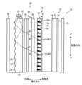
- FIG. 2 is an enlarged view focusing on the optical sheet 30.
- FIG. 1 is a diagram illustrating indentation hardness.
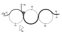
- 3A to 3C are diagrams illustrating a manufacturing process of the optical sheet 30.
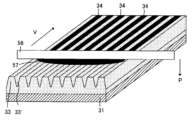
- 3A to 3C are diagrams illustrating a manufacturing process of the optical sheet 30.
- Image source unit Fig. 1 is a diagram for explaining one embodiment, and is an exploded perspective view of an image source unit 10 including an optical sheet 30.
- Fig. 2 shows a part of an exploded cross-sectional view of the image source unit 10 cut along the line II-II (vertical line) shown in Fig. 1
- Fig. 3 shows a part of an exploded cross-sectional view of the image source unit 10 cut along the line III-III (horizontal line).
- an image source unit 10 is housed in a housing (not shown) together with normal equipment required for operating the image source unit 10, such as a power source for operating the image source unit 10 and an electronic circuit for controlling the image source unit 10, to form a display device.
- a liquid crystal image source unit will be described as one embodiment of the image source unit
- a liquid crystal display device will be described as one embodiment of the display device.
- the image source unit 10 will be described below.
- the image source unit 10 includes a liquid crystal panel 15, a surface light source device 20, and a functional film 40.
- the optical sheet 30 is included in the surface light source device 20.
- Figures 1 to 3 also show the orientation of the display device when it is installed.
- the liquid crystal panel 15 has an upper polarizing plate 13 arranged on the viewer side, a lower polarizing plate 14 arranged on the surface light source device 20 side, and a liquid crystal layer 12 arranged between the upper polarizing plate 13 and the lower polarizing plate 14.
- the upper polarizing plate 13 and the lower polarizing plate 14 have the function of decomposing incident light into two orthogonal polarized components (P waves and S waves), transmitting the polarized component in one direction (parallel to the transmission axis) (e.g., P waves) and absorbing the polarized component in the other direction (parallel to the absorption axis) orthogonal to the one direction (e.g., S waves).
- the liquid crystal layer 12 has multiple pixels arranged vertically and horizontally along the layer surface, and an electric field can be applied to each region that forms one pixel.
- the orientation of the pixel to which the electric field is applied changes.
- the polarized component e.g. P wave
- the polarized component parallel to the transmission axis that has passed through the lower polarizer 14 arranged on the surface light source device 20 side (i.e. the light input side) rotates its polarization direction by 90° when passing through a pixel to which an electric field is applied, while maintaining its polarization direction when passing through a pixel to which no electric field is applied. Therefore, depending on whether or not an electric field is applied to the pixel, it is possible to control whether the polarized component (e.g. P wave) that has passed through the lower polarizer 14 is further transmitted through the upper polarizer 13 arranged on the light output side, or is absorbed and blocked by the upper polarizer 13.
- the liquid crystal panel 15 has a structure that controls the transmission or blocking of light from the surface light source device 20 for each pixel to display images.
- liquid crystal panels there are several types of liquid crystal panels, but in this embodiment, the type is not particularly limited, and any known type of liquid crystal panel can be used. Specific examples include TN, STN, VA, MVA, IPS, OCB, etc.
- the surface light source device 20 is an illumination device that is disposed on the opposite side of the liquid crystal panel 15 from the observer side, and emits planar light toward the liquid crystal panel 15.
- the surface light source device 20 of this embodiment is configured as an edge-light type surface light source device, and includes a light guide plate 21, a light source 25, a light diffusion plate 26, a prism layer 27, a reflective polarizing plate 28, an optical sheet 30, and a reflective sheet 39.
- the light guide plate 21 has a base 22 and rear surface optical elements 23.
- the light guide plate 21 is a plate-shaped member made of a light-transmitting material.
- one plate surface side of the light guide plate 21 facing the observer is a smooth surface, and the other plate surface side opposite to this is a rear surface, on which a plurality of rear surface optical elements 23 are arranged.
- thermoplastic resins such as polymer resins with alicyclic structures, methacrylic resins, polycarbonate resins, polystyrene resins, acrylonitrile-styrene copolymers, methyl methacrylate-styrene copolymers, ABS resins, and polyethersulfones, as well as epoxy acrylate and urethane acrylate reactive resins (ionizing radiation curable resins, etc.).
- the base 22 is a plate-like portion with a predetermined thickness through which light is guided and which serves as the base for the rear optical element 23.
- the rear surface optical element 23 is a protruding element formed on the rear surface side of the base 22, and in this embodiment, is a triangular prism.
- the rear surface optical element 23 is a prism with a ridgeline of the protruding apex extending in the horizontal direction, and a plurality of rear surface optical elements 23 are arranged at a predetermined pitch in a direction perpendicular to the extending direction (vertical direction).
- the rear surface optical element 23 in this embodiment has a triangular cross section, but is not limited thereto, and may have any cross section such as a polygonal, hemispherical, part of a sphere, or lens shape.
- the arrangement direction of the multiple rear optical elements 23 is preferably the light guide direction.
- the rear optical elements 23 are arranged in a direction away from the light source 25, and the ridges of the rear optical elements 23 extend parallel to the arrangement direction of the light source 25 or, in the case of a single long light source, the extension direction of the light source.
- triangular shape does not only mean a triangular shape in the strict sense, but also includes an approximate triangular shape that takes into account limitations in manufacturing technology and molding errors.
- terms used in this specification that specify other shapes and geometric conditions, such as “parallel,” “orthogonal,” “ellipse,” and “circle,” are also to be interpreted without being bound by their strict meaning, but with an allowance for errors that may be expected to provide similar optical functions.
- the light guide plate 21 having such a configuration can be manufactured by extrusion molding, or by molding the rear optical elements 23 on the base 22.
- the base 22 and the rear optical elements 23 can be integrally formed.
- the rear optical elements 23 may be made of the same resin material as the base 22, or a different material.
- the light source 25 is disposed on one of the side surfaces (end surfaces) of the base 22 of the light guide plate 21 in the direction in which the rear surface optical elements 23 are arranged.
- the type of light source is not particularly limited, and may be configured in various forms such as a fluorescent lamp such as a linear cold cathode fluorescent tube, a point-shaped LED (light emitting diode), or an incandescent light bulb.
- the light source 25 is configured to be composed of a plurality of LEDs, and is configured so that the turning on and off of each LED and/or the brightness of each LED when turned on can be individually and independently adjusted by a control device (not shown).
- the light source 25 is disposed on one side surface (end surface) as described above, but a light source may also be disposed on the side surface (end surface) opposite to the side surface (end surface).
- the shape of the rear surface optical element is also formed following a known example.
- the light diffusion plate 26 is a layer disposed on the light output side of the light guide plate 21 and has the function of diffusing and outputting the light incident thereon. This can further increase the uniformity of the light output from the light guide plate 21 and make scratches on the light guide plate 21 less noticeable.
- a known light diffusion plate can be used, and for example, a form in which a light diffusion agent is dispersed in a base material can be mentioned.
- the light diffusion plate 26 can be used as a support plate for the prism layer 27.
- the light diffusion plate 26 may be bonded to the light guide plate 21 to be integrated with it.
- the prism layer 27 is provided closer to the liquid crystal panel 15 than the light diffusion plate 26, and is a layer including unit prisms 27a that are convex toward the liquid crystal panel 15.
- the unit prisms 27a have a predetermined cross section and extend in the light guide direction of the light guide plate 21 (vertical direction in this embodiment).
- the multiple unit prisms 27a are arranged in a direction different from the light guide direction (horizontal direction, a direction perpendicular to the light guide direction in a plan view in this embodiment).
- the cross-sectional shape of the unit prism of such a prism layer can be any known shape depending on the required function. Depending on the shape, the light can be further diffused or concentrated.
- the direction in which the unit prisms extend and the direction in which they are arranged are not limited to the above and may be other directions.
- the unit prism may have a predetermined cross section and extend in a direction perpendicular to the light guiding direction of the light guiding plate 21, and a plurality of unit prisms may be arranged in the light guiding direction.
- Reflective polarizing plate 28 has a function of decomposing the incident light into two orthogonal polarized components (P wave and S wave), transmitting the polarized component in one direction (parallel to the transmission axis) (e.g., P wave) and reflecting the polarized component in the other direction (parallel to the reflection axis) orthogonal to the one direction (e.g., S wave).
- P wave and S wave orthogonal polarized components
- Fig. 4 shows an enlarged view of a portion of the optical sheet 30 seen from the perspective of Fig. 2.
- the optical sheet 30 includes a base layer 31 formed in a sheet shape, and an optical function layer 32 provided on one surface of the base layer 31 (the surface on the light guide plate 21 side in this embodiment).
- the base layer 31 is a flat sheet-like member that supports the optical function layer 32 .
- Various materials can be used as the material for the base layer 31.
- materials that are widely used as materials for optical sheets incorporated in display devices, have excellent mechanical properties, optical properties, stability, and processability, and are inexpensively available can be used.
- transparent resin films, transparent resin plates, transparent resin sheets, and transparent glass can be used.
- polyester films such as triacetate cellulose (TAC) films, polyethylene terephthalate (PET), diacetyl cellulose films, acetate butyrate cellulose films, polyethersulfone films, polyacrylic resin films, polyurethane resin films, polyester films, polycarbonate films, polysulfone films, polyether films, polymethylpentene films, polyether ketone films, and (meth)acrylonitrile films can be suitably used, and among these, polyester films are preferably used.
- polyester films in addition to polyethylene terephthalate, polybutylene terephthalate, polynaphthalene terephthalate, polytrimethylene terephthalate, and the like can be used.
- polycarbonate resins with a high glass transition point are desirable.
- the glass transition point of polycarbonate resin is 143° C., which is generally suitable for in-vehicle applications requiring durability at 105° C.
- the optical function layer 32 is a layer laminated on one surface of the base layer 31 (the surface on the light guide plate 21 side in this embodiment), and is configured to have light-transmitting portions 33 and light-absorbing portions 34.
- the optical function layer 32 has a shape that has the cross section shown in Figures 2 and 4 and extends toward the back/front of the page (the horizontal direction when the image source unit 10 is viewed from the front), and the light-transmitting portions 33 and light-absorbing portions 34 are alternately arranged along the layer surface in a direction different from the extending direction (the vertical direction in this embodiment).
- the light-transmitting section 33 is a section whose main function is to transmit light, and in this embodiment, in the cross sections shown in Figures 2 and 4, it is an element having a generally trapezoidal cross-sectional shape with a long lower base on the base layer 31 side and a short upper base on the opposite side (the light guide plate 21 side).
- the light transmitting portions 33 extend in one direction (horizontal direction in this embodiment) while maintaining the cross section along the layer surface of the base material layer 31, and are arranged at a predetermined interval in a direction different from the extending direction (vertical direction in this embodiment).
- a gap (groove) having a substantially trapezoidal cross section is formed between adjacent light transmitting portions 33.
- the gap has a trapezoidal cross section with a long bottom base on the top bottom side (light guide plate 21 side) of the light transmitting portion 33 and a short top base on the bottom bottom side (base material layer 31 side) of the light transmitting portion 33, and the light absorbing portion 34 is formed by filling this with a necessary material described later.
- a plurality of light transmitting portions 33 are connected on their lower bottom sides (base layer side 31) by a sheet-like base portion 32a.
- the light transmitting portion 33 has a refractive index of Nt .
- a light transmitting portion 33 can be formed by curing a light transmitting portion-constituting composition.
- the value of the refractive index Nt is not particularly limited, but from the viewpoint of appropriately reflecting light (including total reflection) at the interface with the light absorbing portion 34 at the inclined surface of the trapezoidal cross section as described below, the refractive index is preferably 1.47 or more. However, since materials with too high a refractive index are often prone to cracking, the refractive index is preferably 1.61 or less. More preferably, it is 1.49 or more and 1.56 or less, and even more preferably 1.56.
- the light absorbing section 34 functions as a gap formed by filling the above-mentioned gap (groove) between adjacent light transmitting sections 33 with a material, and has a basic structure with a cross-sectional shape similar to the cross-sectional shape of the gap. Therefore, in this embodiment, the short upper base faces the liquid crystal panel 15 side (base material layer 31 side), and the long lower base faces the light guide plate 21 side.
- the light absorbing section 34 has a refractive index of Nr and is configured to absorb light. Specifically, light absorbing particles are dispersed in a transparent resin having a refractive index of Nr .
- the refractive index Nr is a refractive index lower than the refractive index Nt of the light transmitting section 33.
- the refractive index of the light absorbing section 34 is not particularly limited, and is preferably 1.47 or more on the premise that the total reflection can be performed appropriately. However, since materials with too high a refractive index are often prone to cracking, the refractive index is preferably 1.61 or less. More preferably, the refractive index is 1.49 or more and 1.56 or less, and even more preferably 1.49.
- the difference in refractive index between the refractive index Nt of the light transmitting portion 33 and the refractive index Nr of the light absorbing portion 34 is not particularly limited, but is preferably greater than 0 and equal to or less than 0.14, and more preferably greater than or equal to 0.05 and equal to or less than 0.14. By increasing the difference in refractive index, more light can be totally reflected.
- the light absorbing portion 34 has interfaces 34a and 34b with the light transmitting portion 33, and the interface angle of the interface 34a is shown as ⁇ 11 in FIG. 4, and the interface angle of the interface 34b is shown as ⁇ 12 in FIG. 4, which are angles formed with the normal line of the layer surface of the optical function layer 32.
- the angles are not particularly limited, but are preferably 0° or more and 10° or less. This makes it possible to increase the brightness in the front direction.
- ⁇ 11 and ⁇ 12 are 0°, the cross sections of the light transmitting portion and the light absorbing portion are rectangular.
- the angles ⁇ 11 and ⁇ 12 may be the same or different.
- the pitch of the light transmitting portion 33 and the light absorbing portion 34 is preferably 20 ⁇ m or more and 100 ⁇ m or less, and more preferably 30 ⁇ m or more and 100 ⁇ m or less.
- the thickness of the light absorbing portion 34, indicated by D in Fig. 4 is preferably 50 ⁇ m or more and 150 ⁇ m or less, and more preferably 60 ⁇ m or more and 150 ⁇ m or less. By setting it within these ranges, it is possible to achieve a more appropriate balance between light transmission and light absorption.
- the light absorption in the light absorbing section 34 can be adjusted by the content ratio of the light absorbing particles in the light absorbing section 34.
- the content ratio of the light absorbing particles to the entire composition (transparent resin + light absorbing particles) constituting the light absorbing section is preferably greater than 10% by mass and less than or equal to 30% by mass. If the content ratio is less than 10% by mass, there is a risk that the light absorbing performance (light blocking properties) of the light absorbing section will be insufficient, and if the content ratio is greater than 30% by mass, there is a risk that the curing property of the light absorbing section will be insufficient, increasing the possibility of problems such as the light absorbing particles falling off.
- the interfaces 34a, 34b between the light transmitting portion 33 and the light absorbing portion 34 are linear in cross section, but the present invention is not limited to this and may be polygonal, convex curved, concave curved, etc.
- the cross-sectional shapes of the multiple light transmitting portions 33 and light absorbing portions 34 may be the same, or may be different cross-sectional shapes with a predetermined regularity.
- the light absorbing portion 34 further has the following characteristics.
- An explanatory diagram is shown in Fig. 5.
- Fig. 5 is a cross section of one light absorbing portion 34, and is a cross section from the same viewpoint as Fig. 4 (a cross section perpendicular to the extension direction of the light absorbing portion 24).
- the light absorbing portion 34 has an indentation hardness H a at a position M a in the cross section, which is greater than an indentation hardness H b at a position M b , that is, H a >H b .
- the indentation hardness Hc at position M c which is located between positions M a and M b
- the indentation hardness is also between H a and H b . That is, it is preferable that H a > H c > H b .
- H c may be smaller than the average value of H a and H b . That is, it is possible to have H a > H b and ⁇ (H a + H b )/2 ⁇ > H c .
- the ratio represented by (H b /H a ) ⁇ 100(%) is 70% or more and 85% or less.
- the ratio represented by (H b /H a ) ⁇ 100(%) is 70% or more and 85% or less, in addition to suppressing warpage, the following effect is achieved.
- An optical sheet having an optical functional layer in which light transmitting portions and light absorbing portions are alternately arranged on a base layer as in the present disclosure can be stored in a rolled state (a state in which a long strip-shaped sheet before being cut into the size of the optical sheet is rolled up) after the light absorbing portions are formed.
- the light transmitting portion has a trapezoidal cross section with a long lower base on the base layer side and a short upper base on the opposite side
- the light absorbing portion has a trapezoidal cross section with a short upper base on the base layer side ( Mb side, Hb side)
- the light absorbing portion on the Mb ( Hb ) side is required to have appropriate flexibility against the stress caused by the roll due to the short upper base.
- the light absorbing portion with the short upper base on the Mb ( Hb ) side is required to have appropriate indentation hardness characteristics.
- Hb satisfies the ratio represented by ( Hb / Ha ) x 100(%) of 70% or more and 85% or less, or, as described below, is 145 MPa or more and 177 MPa or less.
- the magnitude of the indentation hardness H a is not particularly limited, but is preferably 212 MPa or more and 271 MPa or less. This makes it possible to more reliably suppress the occurrence of warping of the optical sheet.
- the magnitude of the indentation hardness H a is more preferably 212 MPa or more and 254 MPa or less.
- the magnitude of the indentation hardness Hb may be any value as long as it satisfies the above-mentioned relationship, and Hb is preferably 145 MPa or more and 177 MPa or less, and more preferably 160 MPa or more and 177 MPa or less.
- the magnitude of the indentation hardness Hc may also satisfy the above-mentioned relationship, and Hc is preferably 149 MPa or more and 213 MPa or less, and more preferably 162 MPa or more and 213 MPa or less.
- the combination of the indentation hardness H a and the indentation hardness H b may be H a >H b , and it is particularly preferable that H a is 158 MPa or more and 271 MPa or less, and H b is 145 MPa or more and 177 MPa or less.
- the positions M a , M b , and M c are defined as follows.
- the center of the bottom (shorter upper base) of the light absorbing portion 34 on the base material layer 31 side is C1
- the center of the bottom (longer lower base) of the light absorbing portion 34 on the opposite side to the base material layer 31 is C2
- the line connecting C1 and C2 is C
- positions M a , M b , and M c are all on line C.
- the centers C 1 and C 2 are considered to be a straight line connecting the ends of the bottom.
- M a is located at a distance of 0.1L A from C 2
- M b is located at a distance of 0.1L A from C 1.
- M c is located in the middle between M a and M b .
- light absorbing particles are present at the positions Ma , Mb , and Mc , the positions closest to the positions except for the light absorbing particles are used.
- the indentation hardness specified in ISO14577-1 is measured in accordance with ISO14577-1 2002-10-01 Part 1, and can be measured, for example, using an ultra-microindentation hardness tester (nanoindentation tester) ENT1100a manufactured by Elionix Co., Ltd., with an indentation load of 10 mgf (divided into 250 steps) and a test load holding time of 1 second.
- an ultra-microindentation hardness tester nanoindentation tester
- ENT1100a manufactured by Elionix Co., Ltd.
- optical sheet manufacturing method The optical sheet 30 as described above can be produced, for example, as follows.
- the light transmitting portion 33 is formed on one surface of the substrate layer 31.
- the substrate sheet 31' to be the substrate layer 31 is inserted between the mold roll 52 having a shape on its surface that can transfer the shape of the light transmitting portion 33 and the nip roll 51 arranged to face it.
- a predetermined gap is provided between the mold roll 52 and the nip roll 51 to form the base portion 32a.
- the mold roll 52 and the nip roll 51 are rotated while supplying the composition constituting the light transmitting portion between the substrate sheet 31' and the mold roll 52 from the supply device 55.
- the composition constituting the light transmitting portion is filled into the grooves (the shape of the unit light transmitting element inverted) corresponding to the unit light transmitting elements formed on the surface of the mold roll 52, and the composition conforms to the surface shape of the mold roll 52.
- the composition constituting the light transmitting portion include ionizing radiation curable resins such as epoxy acrylates, urethane acrylates, polyether acrylates, polyester acrylates, and polythiols.
- the composition that constitutes the light-transmitting portion which is sandwiched between the mold roll 52 and the base sheet 31' and filled therein, is irradiated with light from the base sheet side by the light irradiation device 54 for hardening. This hardens the composition and fixes its shape. Then, the base layer 31 and the molded light-transmitting portion 33 are released from the mold roll 52 by the release roll 53.
- the light absorbing portions 34 are formed.
- the gaps (grooves) between the light transmitting portions 33 formed above are filled with the ink composition 57 that constitutes the light absorbing portions.
- excess composition is scraped off with a doctor blade 58 or the like.
- the remaining ink composition is cured by irradiating it with ultraviolet light from the unit light transmitting element 33 side, thereby forming the light absorbing portions 34.
- this can be performed, for example, as follows.
- the grooves 33' between the parallel light-transmitting portions 33 are filled with an ink composition 57 containing a transparent ionizing radiation resin composition and light-absorbing particles.
- the ink composition 57 can be filled into the wedge-shaped grooves by, for example, dropping with a dispenser, applying with a die head, or using a finisher roll.
- the ink composition contains a transparent ionizing radiation curable resin composition and light absorbing particles as components.
- a transparent ionizing radiation curable resin composition a conventionally known ionizing radiation curable resin composition used in a visibility improving sheet, a viewing angle improving sheet, etc. can be used.
- a resin having an acrylate-based functional group can be suitably used, and specific examples thereof include oligomers or prepolymers such as (meth)acrylates of polyfunctional compounds such as relatively low molecular weight polyester resins, polyether resins, acrylic resins, epoxy resins, urethane resins, alkyd resins, spiroacetal resins, polybutadiene resins, polythiolpolyene resins, and polyhydric alcohols.
- a reactive diluent may be added to the resin composition.
- a monofunctional monomer or a polyfunctional monomer such as ethyl (meth)acrylate, ethylhexyl (meth)acrylate, styrene, methylstyrene, or N-vinylpyrrolidone may be used.
- the reactive diluent include trimethylolpropane tri(meth)acrylate, hexanediol (meth)acrylate, tripropylene glycol di(meth)acrylate, diethylene glycol di(meth)acrylate, pentaerythritol tri(meth)acrylate, dipentaerythritol hexa(meth)acrylate, 1,6-hexanediol di(meth)acrylate, and neopentyl glycol di(meth)acrylate.
- acetophenones, benzophenones, Michler's benzoyl benzoate, ⁇ -amyloxime ester, tetramethylthiuram monosulfide, thioxanthones, etc. as photopolymerization initiators, or n-butylamine, triethylamine, poly-n-butylphosphine, etc. as photosensitizers can be mixed into the composition.
- resin beads or glass beads may be used, and colored particles capable of selectively absorbing a specific wavelength in accordance with the characteristics of the image light may be used.
- Colorants such as carbon black, graphite, fibrous carbon, metal salts such as black iron oxide, dyes, pigments, etc. may be kneaded into the resin beads or glass beads. From the viewpoint of ease of kneading the colorant, it is preferable to use resin beads.
- resin beads melamine beads, acrylic beads, acrylic-styrene beads, polycarbonate beads, polyethylene beads, polystyrene beads, PVC beads, etc. can be suitably used.
- urethane crosslinked fine particles and silicon-based beads can also be suitably used.
- the resin before kneading the colorant a transparent resin can be used, but it is preferable to use a resin colored with a pigment or dye, etc., and it may be a resin that selectively absorbs a specific wavelength in accordance with the characteristics of the image light, but preferably resin beads colored black are used.
- the average particle diameter of the light absorbing particles is preferably 1.0 ⁇ m or more and 20 ⁇ m or less, more preferably 1.0 ⁇ m or more and 10 ⁇ m or less, and even more preferably 1.0 ⁇ m or more and 4.0 ⁇ m or less.
- average particle diameter refers to the diameter obtained by observing 100 light absorbing particles with an electron microscope, measuring their diameters, and arithmetically averaging them.
- carbon black can be preferably used among the above-mentioned.
- the amount of carbon black kneaded into the resin beads is about 0.1 to 0.7 parts by mass, preferably 0.15 to 0.5 parts by mass, and more preferably 0.2 to 0.35 parts by mass, per 1 part by mass of the resin beads. If the amount of carbon black kneaded is more than 0.7 parts by mass, the resin beads may be easily broken, while if it is less than 0.1 parts by mass, fine particles having the desired blackness may not be obtained.
- carbon black having an average particle size of 10 to 500 nm can be preferably used, and for example, furnace black, acetylene black, channel black, thermal black, carbon nanotube, carbon fiber, etc. can be used.
- the average particle size here means the arithmetic mean diameter determined by observing carbon black particles under an electron microscope.
- the particles may be surface-treated in advance, for example, by a conventionally known hydrophilic treatment using silica coating or surface modification using plasma or the like.
- the ink composition containing the above-mentioned components is prepared by mixing a predetermined amount of light-absorbing particles with an ionizing radiation curable resin composition, and adding a polymerization initiator, etc., if desired.
- the amount of colored fine particles added is preferably in the range of 15 to 35% of the total mass of the ink composition, and by setting it in this range, a visibility improving sheet with better contrast can be realized. If the content of the light-absorbing particles is too small, the light blocking ability of the light-absorbing part may be insufficient, and if the content of the light-absorbing particles is too large, the resin beads come into contact with each other, easily causing problems such as cracking and chipping.
- the excess ink composition 57 is scraped off with a doctor blade 58 as shown in FIG. 7 so that the ink composition 57 fills the grooves 33'.
- the ink composition 57 is scraped off by the doctor blade 58 by pressing the doctor blade 58 against the light-transmitting portion 33 with a predetermined pressure (pressing force) while moving the laminate of the base layer 31 and the light-transmitting portion 33 at a predetermined speed V.
- the curing method can be by irradiation with electron beams or ultraviolet rays.
- electron beam curing an electron beam having an energy of 50 to 1000 keV, preferably 100 to 300 keV, emitted from various electron beam accelerators such as Cockcroft-Walton type, Van de Graaff type, resonant transformer type, insulating core transformer type, linear type, dynamitron type, and high frequency type, etc.
- ultraviolet ray curing ultraviolet emitted from light beams of ultra-high pressure mercury lamps, high pressure mercury lamps, low pressure mercury lamps, carbon arcs, xenon arcs, metal halide lamps, etc. can be used.
- the dose of the electron beam or ultraviolet light to be irradiated can be reduced and the
- the reflective sheet 39 of the surface light source device 20 will be described.
- the reflective sheet 39 is a member for reflecting light emitted from the rear surface of the light guide plate 21 and causing the light to enter the light guide plate 21 again.
- a sheet capable of so-called specular reflection such as a sheet made of a material having a high reflectance such as a metal, or a sheet including a thin film (e.g., a metal thin film) made of a material having a high reflectance as a surface layer, can be preferably used.
- the functional film 40 is disposed on the light output side of the liquid crystal panel 15, and is a layer having the function of improving the quality of the image light and protecting the image source unit 10.
- a layer include an anti-reflection film, an anti-glare film, a hard coat film, a color correction film, and a light diffusion film, and these may be used alone or in combination.
- optical sheet 30 having the above-mentioned configuration
- the examples of optical paths are conceptual examples for the purpose of explanation, and do not strictly represent the degree of reflection or refraction.
- FIG. 2 shows, as an example, an example of the optical path of light L21, L22 entering the light guide plate 21 from the light source 25.
- the light L21 and L22 incident on the light guide plate 21 are repeatedly totally reflected on the light-emitting side of the light guide plate 21 and on the back surface on the opposite side due to the difference in refractive index with air, and proceed in the light guide direction (downward in the plane of the paper in FIG. 2).
- a rear optical element 23 is disposed on the rear surface of the light guide plate 21. Therefore, as shown in FIG. 2, the direction of light L21, L22 traveling inside the light guide plate 21 may change due to the rear optical element 23, and may be incident on the light output surface and rear surface at an angle of incidence less than the critical angle of total reflection. In this case, the light may be emitted from the light output surface of the light guide plate 21 and the rear surface on the opposite side.
- the light L21 and L22 emitted from the light output surface travels toward the light diffusion plate 26 arranged on the light output side of the light guide plate 21.
- the light emitted from the rear surface is reflected by the reflective sheet 39 arranged on the rear surface of the light guide plate 21, and enters the light guide plate 21 again to travel within the light guide plate 21.
- the light traveling through the light guide plate 21 and the light that is redirected by the rear optical element 23 and reaches the light output surface at an angle of incidence less than the critical angle of total reflection are generated in each area along the light guide direction within the light guide plate 21.
- the light traveling through the light guide plate 21 is gradually emitted from the light output surface. This makes it possible to uniformize the light amount distribution along the light guide direction of the light that is emitted from the light output surface of the light guide plate 21.
- the light emitted from the light guide plate 21 then reaches the light diffusion plate 26, where the uniformity is increased.
- the light is then diffused or concentrated as necessary by the prism layer 27, and the light that has exited the prism layer 27 reaches the reflective polarizing plate 28.
- the light polarized in the direction along the transmission axis of the reflective polarizing plate 28 passes through the reflective polarizing plate 28 and travels toward the optical sheet 30.
- light polarized in the direction along the reflection axis of reflective polarizer 28 is reflected as shown by the dotted arrow in Fig. 2 and returned to the light guide plate 21 side.
- the returned light is reflected by the light guide plate 21, rear optical element 23, or reflective sheet 39 and travels again toward the reflective polarizer 28 side.
- the polarization direction of some of the light changes, and some of this light passes through reflective polarizer 28.
- the other light is returned again to the light guide plate side.
- the light reflected by reflective polarizer 28 can also pass through reflective polarizer 28 by repeating reflections. This increases the utilization rate of light from light source 25.
- the polarization direction of the light emitted from the reflective polarizing plate 28 is aligned along the transmission axis of the lower polarizing plate 14 , and the light becomes polarized light that passes through the lower polarizing plate 14 .
- the light that leaves the reflective polarizing plate 28 reaches the optical sheet 30.
- the light that enters the optical sheet 30 travels along the following optical path.
- An example of the optical path in the optical sheet 30 is shown in Figure 4.
- the light travels toward the interface between the light transmitting portions 33 and the light absorbing portions 34, as with the light L21 and light L22 shown in Fig. 2 and the light L41 and light L42 shown in Fig. 4. Then, the light is totally reflected at the interface, and the light is controlled to travel in a desired direction so that the viewing angle is limited. If necessary, the angle of the interface between the light-transmitting portion 33 and the light-absorbing portion 34 ( ⁇ 11 , ⁇ 12 in FIG. 4 ) can be adjusted to direct the light in a direction having a desired angle with respect to the normal direction of the optical sheet (i.e., the front direction).
- L43 shown in FIG. 4 travels at an angle that transmits through the interface between the light transmitting portion 33 and the light absorbing portion 34 without being totally reflected at the interface, and is therefore transmitted through the interface and absorbed by the light absorbing portion 34.
- This makes it possible to efficiently absorb and block light that is emitted at a viewing angle of a predetermined angle or more, thereby limiting the viewing angle.
- since such light is highly likely to enter the liquid crystal panel and cause problems such as reduced contrast and color inversion, it is possible to absorb such light.
- the light that exits the optical sheet 30 is incident on the lower polarizer 14 of the liquid crystal panel 15.
- the lower polarizer 14 transmits one polarized component of the incident light and absorbs the other polarized component.
- the light that passes through the lower polarizer 14 selectively passes through the upper polarizer 13 depending on the state of the electric field applied to each pixel.
- the liquid crystal panel 15 selectively transmits the light from the surface light source device 20 for each pixel, allowing the viewer of the liquid crystal display device to view an image. At that time, the image light is provided to the viewer via the functional film 40, improving the quality of the image.
- warping can be suppressed by adjusting the indentation hardness of the light absorbing parts. If warping can be suppressed in this way with the light absorbing parts, a surface light source device can be constructed without adding additional layers, or even if additional layers are added, without adding thick layers, and without necessarily gluing layers together, allowing for a thin structure and high flexibility in layer configuration. However, this does not prevent the application of warping suppression by conventional means in addition to the application of the configuration of the present disclosure.
- Base material layer Thickness: 250 ⁇ m
- Material Polycarbonate
- Light-transmitting portion material Epoxy acrylate
- Light-absorbing portion shape Isosceles trapezoid with lower base (W b ) 22 ⁇ m, upper base (W a ) 3 ⁇ m, height (D) 120 ⁇ m, and inclination angle ( ⁇ 11 , ⁇ 12 ) 4.5°
- Pitch P a of light-absorbing portion 47 ⁇ m
- Light absorbing material Acrylic beads (black) dispersed in acrylic resin binder. Acrylic beads: average particle size 4 ⁇ m, 2 parts by weight per 100 parts by weight of binder.
- the optical sheet was manufactured according to the procedure described above.
- the indentation hardness of the light absorbing portion in each example was adjusted by changing the amount of ultraviolet light irradiation (low pressure mercury lamp) for each example, when irradiating ultraviolet light from both the upper and lower sides of the light absorbing portion.
- Specific irradiation amounts are shown in Table 1. In Table 1, the amounts are expressed as a ratio when the amount of ultraviolet light irradiation in Comparative Example 1 is set to 1.
- the indentation hardness was measured as described above, and the average value of five measurements was used.
- the warping of the optical sheet was evaluated by exposing the optical sheet to an air atmosphere at a temperature of 70°C and a humidity of 95% for 1,000 hours, and then leaving it on a flat table at room temperature and humidity for 24 hours, and measuring the distance from the surface of the table to the four corners of the optical film using a JIS Class 1 straightedge.
- Table 1 shows the results, including the indentation hardness (MPa), the ratio (%) of the indentation hardness at each position for each example when H a is set to 100, the warpage (mm), and the value of H b /H a ⁇ 100%.
- 10 image source unit, 15...liquid crystal panel, 20...surface light source device, 21...light guide plate, 25...light source, 26...light diffusion plate, 27...prism layer, 28...reflective polarizing plate, 30...optical sheet, 31...base material layer, 32...optical function layer, 33...light transmission section, 34...light absorption section
Landscapes
- Physics & Mathematics (AREA)
- General Physics & Mathematics (AREA)
- Optics & Photonics (AREA)
- Optical Elements Other Than Lenses (AREA)
- Laminated Bodies (AREA)
Abstract
L'invention concerne une feuille optique qui a une couche dans laquelle une partie de transmission de lumière et une partie d'absorption de lumière sont disposées en alternance, et qui est capable de supprimer un gauchissement tout en fixant un degré de liberté en configuration de couche. La feuille optique a une couche de matériau de base et une couche fonctionnelle optique qui est stratifiée sur la couche de matériau de base et dans laquelle une partie de transmission de lumière et une partie d'absorption de lumière sont disposées en alternance, la couche de fonction optique étant configurée de telle sorte que : la partie de transmission de lumière a une section transversale prédéterminée et s'étend dans une direction, et une pluralité des parties de transmission de lumière sont disposées à des intervalles dans une direction différente de la direction ; et la partie d'absorption de lumière est disposée entre les parties de transmission de lumière, et lorsque la dureté d'indentation de la partie d'absorption de lumière à une position Mb sur le côté de la couche de matériau de base est notée Hb et la dureté d'indentation à une position Ma sur le côté opposé à la couche de matériau de base est notée Ha, Ha > Hb est satisfaite.
Applications Claiming Priority (2)
| Application Number | Priority Date | Filing Date | Title |
|---|---|---|---|
| JP2023-108042 | 2023-06-30 | ||
| JP2023108042 | 2023-06-30 |
Publications (1)
| Publication Number | Publication Date |
|---|---|
| WO2025005116A1 true WO2025005116A1 (fr) | 2025-01-02 |
Family
ID=93939271
Family Applications (1)
| Application Number | Title | Priority Date | Filing Date |
|---|---|---|---|
| PCT/JP2024/023130 Ceased WO2025005116A1 (fr) | 2023-06-30 | 2024-06-26 | Feuille optique |
Country Status (2)
| Country | Link |
|---|---|
| TW (1) | TW202508813A (fr) |
| WO (1) | WO2025005116A1 (fr) |
Citations (2)
| Publication number | Priority date | Publication date | Assignee | Title |
|---|---|---|---|---|
| JP2018112618A (ja) * | 2017-01-10 | 2018-07-19 | 大日本印刷株式会社 | 映像源ユニット、及び表示装置 |
| JP2023040121A (ja) * | 2017-03-31 | 2023-03-22 | 大日本印刷株式会社 | 光学シート、光制御部材、面光源装置、映像源ユニット、及び表示装置 |
-
2024
- 2024-06-26 WO PCT/JP2024/023130 patent/WO2025005116A1/fr not_active Ceased
- 2024-06-27 TW TW113124000A patent/TW202508813A/zh unknown
Patent Citations (2)
| Publication number | Priority date | Publication date | Assignee | Title |
|---|---|---|---|---|
| JP2018112618A (ja) * | 2017-01-10 | 2018-07-19 | 大日本印刷株式会社 | 映像源ユニット、及び表示装置 |
| JP2023040121A (ja) * | 2017-03-31 | 2023-03-22 | 大日本印刷株式会社 | 光学シート、光制御部材、面光源装置、映像源ユニット、及び表示装置 |
Also Published As
| Publication number | Publication date |
|---|---|
| TW202508813A (zh) | 2025-03-01 |
Similar Documents
| Publication | Publication Date | Title |
|---|---|---|
| JP7768263B2 (ja) | 光学シート、光制御部材、面光源装置、映像源ユニット、及び表示装置 | |
| JP5686135B2 (ja) | 表示装置 | |
| KR101830969B1 (ko) | 고투과 광 제어 필름 | |
| KR101450020B1 (ko) | 확산 시트 및 그것을 이용한 백라이트 유닛 | |
| KR20130041215A (ko) | 광확산 필름 및 그의 제조 방법, 광확산성 편광판 및 액정 표시 장치 | |
| US9563004B2 (en) | Image source unit and image display unit | |
| US11243343B2 (en) | Backlight unit and liquid crystal display device | |
| KR20110102897A (ko) | 광학 필름 및 이를 포함하는 액정 표시 장치 | |
| JP6880612B2 (ja) | 映像源ユニット、及び表示装置 | |
| JP6933005B2 (ja) | 光学シート、映像源ユニット及び液晶表示装置 | |
| JP2017198735A (ja) | 光学シート、映像源ユニット及び液晶表示装置 | |
| JP7000781B2 (ja) | 光学シート、面光源装置、映像源ユニット、及び表示装置 | |
| JP2017045060A (ja) | 光学シート、面光源装置、映像源ユニット、表示装置、及び光学シートの製造方法。 | |
| WO2025005116A1 (fr) | Feuille optique | |
| JP2018112618A (ja) | 映像源ユニット、及び表示装置 | |
| JP7244204B2 (ja) | 光学シート、面光源装置、映像源ユニット、及び表示装置 | |
| JP2018109677A (ja) | 光学シート、映像源ユニット、及び液晶表示装置 | |
| JP6915296B2 (ja) | 光学ユニット、面光源装置、映像源ユニット、及び液晶表示装置 | |
| JP7135294B2 (ja) | 光学シート、面光源装置、映像源ユニット、及び表示装置 | |
| JP2024167035A (ja) | 光学シート、面光源装置および表示装置 |
Legal Events
| Date | Code | Title | Description |
|---|---|---|---|
| 121 | Ep: the epo has been informed by wipo that ep was designated in this application |
Ref document number: 24831975 Country of ref document: EP Kind code of ref document: A1 |
|
| NENP | Non-entry into the national phase |
Ref country code: DE |