WO2025013292A1 - 切削工具 - Google Patents
切削工具 Download PDFInfo
- Publication number
- WO2025013292A1 WO2025013292A1 PCT/JP2023/025928 JP2023025928W WO2025013292A1 WO 2025013292 A1 WO2025013292 A1 WO 2025013292A1 JP 2023025928 W JP2023025928 W JP 2023025928W WO 2025013292 A1 WO2025013292 A1 WO 2025013292A1
- Authority
- WO
- WIPO (PCT)
- Prior art keywords
- layer
- particle layer
- hard particle
- hard
- region
- Prior art date
- Legal status (The legal status is an assumption and is not a legal conclusion. Google has not performed a legal analysis and makes no representation as to the accuracy of the status listed.)
- Pending
Links
Images


Classifications
-
- B—PERFORMING OPERATIONS; TRANSPORTING
- B23—MACHINE TOOLS; METAL-WORKING NOT OTHERWISE PROVIDED FOR
- B23B—TURNING; BORING
- B23B27/00—Tools for turning or boring machines; Tools of a similar kind in general; Accessories therefor
- B23B27/14—Cutting tools of which the bits or tips or cutting inserts are of special material
- B23B27/148—Composition of the cutting inserts
-
- C—CHEMISTRY; METALLURGY
- C23—COATING METALLIC MATERIAL; COATING MATERIAL WITH METALLIC MATERIAL; CHEMICAL SURFACE TREATMENT; DIFFUSION TREATMENT OF METALLIC MATERIAL; COATING BY VACUUM EVAPORATION, BY SPUTTERING, BY ION IMPLANTATION OR BY CHEMICAL VAPOUR DEPOSITION, IN GENERAL; INHIBITING CORROSION OF METALLIC MATERIAL OR INCRUSTATION IN GENERAL
- C23C—COATING METALLIC MATERIAL; COATING MATERIAL WITH METALLIC MATERIAL; SURFACE TREATMENT OF METALLIC MATERIAL BY DIFFUSION INTO THE SURFACE, BY CHEMICAL CONVERSION OR SUBSTITUTION; COATING BY VACUUM EVAPORATION, BY SPUTTERING, BY ION IMPLANTATION OR BY CHEMICAL VAPOUR DEPOSITION, IN GENERAL
- C23C16/00—Chemical coating by decomposition of gaseous compounds, without leaving reaction products of surface material in the coating, i.e. chemical vapour deposition [CVD] processes
- C23C16/22—Chemical coating by decomposition of gaseous compounds, without leaving reaction products of surface material in the coating, i.e. chemical vapour deposition [CVD] processes characterised by the deposition of inorganic material, other than metallic material
- C23C16/30—Deposition of compounds, mixtures or solid solutions, e.g. borides, carbides, nitrides
- C23C16/34—Nitrides
-
- C—CHEMISTRY; METALLURGY
- C23—COATING METALLIC MATERIAL; COATING MATERIAL WITH METALLIC MATERIAL; CHEMICAL SURFACE TREATMENT; DIFFUSION TREATMENT OF METALLIC MATERIAL; COATING BY VACUUM EVAPORATION, BY SPUTTERING, BY ION IMPLANTATION OR BY CHEMICAL VAPOUR DEPOSITION, IN GENERAL; INHIBITING CORROSION OF METALLIC MATERIAL OR INCRUSTATION IN GENERAL
- C23C—COATING METALLIC MATERIAL; COATING MATERIAL WITH METALLIC MATERIAL; SURFACE TREATMENT OF METALLIC MATERIAL BY DIFFUSION INTO THE SURFACE, BY CHEMICAL CONVERSION OR SUBSTITUTION; COATING BY VACUUM EVAPORATION, BY SPUTTERING, BY ION IMPLANTATION OR BY CHEMICAL VAPOUR DEPOSITION, IN GENERAL
- C23C16/00—Chemical coating by decomposition of gaseous compounds, without leaving reaction products of surface material in the coating, i.e. chemical vapour deposition [CVD] processes
- C23C16/22—Chemical coating by decomposition of gaseous compounds, without leaving reaction products of surface material in the coating, i.e. chemical vapour deposition [CVD] processes characterised by the deposition of inorganic material, other than metallic material
- C23C16/30—Deposition of compounds, mixtures or solid solutions, e.g. borides, carbides, nitrides
- C23C16/36—Carbonitrides
-
- C—CHEMISTRY; METALLURGY
- C23—COATING METALLIC MATERIAL; COATING MATERIAL WITH METALLIC MATERIAL; CHEMICAL SURFACE TREATMENT; DIFFUSION TREATMENT OF METALLIC MATERIAL; COATING BY VACUUM EVAPORATION, BY SPUTTERING, BY ION IMPLANTATION OR BY CHEMICAL VAPOUR DEPOSITION, IN GENERAL; INHIBITING CORROSION OF METALLIC MATERIAL OR INCRUSTATION IN GENERAL
- C23C—COATING METALLIC MATERIAL; COATING MATERIAL WITH METALLIC MATERIAL; SURFACE TREATMENT OF METALLIC MATERIAL BY DIFFUSION INTO THE SURFACE, BY CHEMICAL CONVERSION OR SUBSTITUTION; COATING BY VACUUM EVAPORATION, BY SPUTTERING, BY ION IMPLANTATION OR BY CHEMICAL VAPOUR DEPOSITION, IN GENERAL
- C23C16/00—Chemical coating by decomposition of gaseous compounds, without leaving reaction products of surface material in the coating, i.e. chemical vapour deposition [CVD] processes
- C23C16/22—Chemical coating by decomposition of gaseous compounds, without leaving reaction products of surface material in the coating, i.e. chemical vapour deposition [CVD] processes characterised by the deposition of inorganic material, other than metallic material
- C23C16/30—Deposition of compounds, mixtures or solid solutions, e.g. borides, carbides, nitrides
- C23C16/40—Oxides
- C23C16/403—Oxides of aluminium, magnesium or beryllium
-
- C—CHEMISTRY; METALLURGY
- C23—COATING METALLIC MATERIAL; COATING MATERIAL WITH METALLIC MATERIAL; CHEMICAL SURFACE TREATMENT; DIFFUSION TREATMENT OF METALLIC MATERIAL; COATING BY VACUUM EVAPORATION, BY SPUTTERING, BY ION IMPLANTATION OR BY CHEMICAL VAPOUR DEPOSITION, IN GENERAL; INHIBITING CORROSION OF METALLIC MATERIAL OR INCRUSTATION IN GENERAL
- C23C—COATING METALLIC MATERIAL; COATING MATERIAL WITH METALLIC MATERIAL; SURFACE TREATMENT OF METALLIC MATERIAL BY DIFFUSION INTO THE SURFACE, BY CHEMICAL CONVERSION OR SUBSTITUTION; COATING BY VACUUM EVAPORATION, BY SPUTTERING, BY ION IMPLANTATION OR BY CHEMICAL VAPOUR DEPOSITION, IN GENERAL
- C23C28/00—Coating for obtaining at least two superposed coatings either by methods not provided for in a single one of groups C23C2/00 - C23C26/00 or by combinations of methods provided for in subclasses C23C and C25C or C25D
- C23C28/04—Coating for obtaining at least two superposed coatings either by methods not provided for in a single one of groups C23C2/00 - C23C26/00 or by combinations of methods provided for in subclasses C23C and C25C or C25D only coatings of inorganic non-metallic material
- C23C28/042—Coating for obtaining at least two superposed coatings either by methods not provided for in a single one of groups C23C2/00 - C23C26/00 or by combinations of methods provided for in subclasses C23C and C25C or C25D only coatings of inorganic non-metallic material including a refractory ceramic layer, e.g. refractory metal oxides, ZrO2, rare earth oxides
-
- C—CHEMISTRY; METALLURGY
- C23—COATING METALLIC MATERIAL; COATING MATERIAL WITH METALLIC MATERIAL; CHEMICAL SURFACE TREATMENT; DIFFUSION TREATMENT OF METALLIC MATERIAL; COATING BY VACUUM EVAPORATION, BY SPUTTERING, BY ION IMPLANTATION OR BY CHEMICAL VAPOUR DEPOSITION, IN GENERAL; INHIBITING CORROSION OF METALLIC MATERIAL OR INCRUSTATION IN GENERAL
- C23C—COATING METALLIC MATERIAL; COATING MATERIAL WITH METALLIC MATERIAL; SURFACE TREATMENT OF METALLIC MATERIAL BY DIFFUSION INTO THE SURFACE, BY CHEMICAL CONVERSION OR SUBSTITUTION; COATING BY VACUUM EVAPORATION, BY SPUTTERING, BY ION IMPLANTATION OR BY CHEMICAL VAPOUR DEPOSITION, IN GENERAL
- C23C28/00—Coating for obtaining at least two superposed coatings either by methods not provided for in a single one of groups C23C2/00 - C23C26/00 or by combinations of methods provided for in subclasses C23C and C25C or C25D
- C23C28/04—Coating for obtaining at least two superposed coatings either by methods not provided for in a single one of groups C23C2/00 - C23C26/00 or by combinations of methods provided for in subclasses C23C and C25C or C25D only coatings of inorganic non-metallic material
- C23C28/044—Coating for obtaining at least two superposed coatings either by methods not provided for in a single one of groups C23C2/00 - C23C26/00 or by combinations of methods provided for in subclasses C23C and C25C or C25D only coatings of inorganic non-metallic material coatings specially adapted for cutting tools or wear applications
-
- C—CHEMISTRY; METALLURGY
- C23—COATING METALLIC MATERIAL; COATING MATERIAL WITH METALLIC MATERIAL; CHEMICAL SURFACE TREATMENT; DIFFUSION TREATMENT OF METALLIC MATERIAL; COATING BY VACUUM EVAPORATION, BY SPUTTERING, BY ION IMPLANTATION OR BY CHEMICAL VAPOUR DEPOSITION, IN GENERAL; INHIBITING CORROSION OF METALLIC MATERIAL OR INCRUSTATION IN GENERAL
- C23C—COATING METALLIC MATERIAL; COATING MATERIAL WITH METALLIC MATERIAL; SURFACE TREATMENT OF METALLIC MATERIAL BY DIFFUSION INTO THE SURFACE, BY CHEMICAL CONVERSION OR SUBSTITUTION; COATING BY VACUUM EVAPORATION, BY SPUTTERING, BY ION IMPLANTATION OR BY CHEMICAL VAPOUR DEPOSITION, IN GENERAL
- C23C28/00—Coating for obtaining at least two superposed coatings either by methods not provided for in a single one of groups C23C2/00 - C23C26/00 or by combinations of methods provided for in subclasses C23C and C25C or C25D
- C23C28/04—Coating for obtaining at least two superposed coatings either by methods not provided for in a single one of groups C23C2/00 - C23C26/00 or by combinations of methods provided for in subclasses C23C and C25C or C25D only coatings of inorganic non-metallic material
- C23C28/048—Coating for obtaining at least two superposed coatings either by methods not provided for in a single one of groups C23C2/00 - C23C26/00 or by combinations of methods provided for in subclasses C23C and C25C or C25D only coatings of inorganic non-metallic material with layers graded in composition or physical properties
-
- C—CHEMISTRY; METALLURGY
- C23—COATING METALLIC MATERIAL; COATING MATERIAL WITH METALLIC MATERIAL; CHEMICAL SURFACE TREATMENT; DIFFUSION TREATMENT OF METALLIC MATERIAL; COATING BY VACUUM EVAPORATION, BY SPUTTERING, BY ION IMPLANTATION OR BY CHEMICAL VAPOUR DEPOSITION, IN GENERAL; INHIBITING CORROSION OF METALLIC MATERIAL OR INCRUSTATION IN GENERAL
- C23C—COATING METALLIC MATERIAL; COATING MATERIAL WITH METALLIC MATERIAL; SURFACE TREATMENT OF METALLIC MATERIAL BY DIFFUSION INTO THE SURFACE, BY CHEMICAL CONVERSION OR SUBSTITUTION; COATING BY VACUUM EVAPORATION, BY SPUTTERING, BY ION IMPLANTATION OR BY CHEMICAL VAPOUR DEPOSITION, IN GENERAL
- C23C28/00—Coating for obtaining at least two superposed coatings either by methods not provided for in a single one of groups C23C2/00 - C23C26/00 or by combinations of methods provided for in subclasses C23C and C25C or C25D
- C23C28/40—Coatings including alternating layers following a pattern, a periodic or defined repetition
- C23C28/42—Coatings including alternating layers following a pattern, a periodic or defined repetition characterized by the composition of the alternating layers
-
- C—CHEMISTRY; METALLURGY
- C23—COATING METALLIC MATERIAL; COATING MATERIAL WITH METALLIC MATERIAL; CHEMICAL SURFACE TREATMENT; DIFFUSION TREATMENT OF METALLIC MATERIAL; COATING BY VACUUM EVAPORATION, BY SPUTTERING, BY ION IMPLANTATION OR BY CHEMICAL VAPOUR DEPOSITION, IN GENERAL; INHIBITING CORROSION OF METALLIC MATERIAL OR INCRUSTATION IN GENERAL
- C23C—COATING METALLIC MATERIAL; COATING MATERIAL WITH METALLIC MATERIAL; SURFACE TREATMENT OF METALLIC MATERIAL BY DIFFUSION INTO THE SURFACE, BY CHEMICAL CONVERSION OR SUBSTITUTION; COATING BY VACUUM EVAPORATION, BY SPUTTERING, BY ION IMPLANTATION OR BY CHEMICAL VAPOUR DEPOSITION, IN GENERAL
- C23C30/00—Coating with metallic material characterised only by the composition of the metallic material, i.e. not characterised by the coating process
- C23C30/005—Coating with metallic material characterised only by the composition of the metallic material, i.e. not characterised by the coating process on hard metal substrates
-
- B—PERFORMING OPERATIONS; TRANSPORTING
- B23—MACHINE TOOLS; METAL-WORKING NOT OTHERWISE PROVIDED FOR
- B23B—TURNING; BORING
- B23B2228/00—Properties of materials of tools or workpieces, materials of tools or workpieces applied in a specific manner
- B23B2228/10—Coatings
- B23B2228/105—Coatings with specified thickness
Definitions
- This disclosure relates to cutting tools.
- the cutting tool of the present disclosure comprises: 1.
- a cutting tool comprising a substrate and a coating disposed on the substrate,
- the coating includes a hard particle layer, the hard particle layer is made of a plurality of hard particles made of titanium, silicon, carbon and nitrogen;
- the hard particle layer includes a first region and a second region, the first region is a region sandwiched between a first main surface of the hard particle layer on the substrate side and a virtual surface S1 that is spaced 0.5 ⁇ m from the first main surface toward the hard particle layer side, the second region is a region sandwiched between a second main surface of the hard particle layer opposite to the first main surface and a virtual surface S2 that is spaced 0.5 ⁇ m from the second main surface toward the hard particle layer,
- the composition of the first region is Ti (1-Xb) SiXbCN
- the composition of the second region is Ti (1-Xs) SiXsCN ,
- the Xs and Xb satisfy the relationships of Xs-Xb ⁇ 0.01 and
- FIG. 1 is a schematic diagram showing an example of a cross section of a cutting tool according to a first embodiment.
- FIG. 2 is a schematic view showing another example of a cross section of the cutting tool according to the first embodiment.
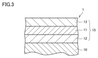
- FIG. 3 is a schematic view showing another example of a cross section of the cutting tool according to the first embodiment.
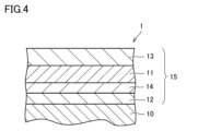
- FIG. 4 is a schematic view showing another example of a cross section of the cutting tool according to the first embodiment.
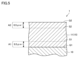
- FIG. 5 is a schematic view showing another example of a cross section of the cutting tool according to the first embodiment.
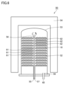
- FIG. 6 is a schematic cross-sectional view of an example of a CVD apparatus used in the manufacture of the cutting tool according to the second embodiment.
- the cutting tool of Patent Document 1 has a high hardness TiSiCN film, and therefore has excellent wear resistance.
- FCD700 spheroidal graphite cast iron
- the tool life may be shortened due to destruction of the coating. For this reason, there is a demand for a cutting tool that can have a long tool life, especially when cutting a workpiece having high cutting resistance.
- the present disclosure therefore aims to provide a cutting tool that can have a long tool life, particularly when cutting workpieces that have high cutting resistance.
- the cutting tool of the present disclosure comprises: 1. A cutting tool comprising a substrate and a coating disposed on the substrate, The coating includes a hard particle layer, the hard particle layer is made of a plurality of hard particles made of titanium, silicon, carbon and nitrogen; the hard particle layer includes a first region and a second region, the first region is a region sandwiched between a first main surface of the hard particle layer on the substrate side and a virtual surface S1 that is spaced 0.5 ⁇ m from the first main surface toward the hard particle layer side, the second region is a region sandwiched between a second main surface of the hard particle layer opposite to the first main surface and a virtual surface S2 that is spaced 0.5 ⁇ m from the second main surface toward the hard particle layer,
- the composition of the first region is Ti (1-Xb) SiXbCN
- the composition of the second region is Ti (1-Xs) SiXsCN , The Xs and
- This disclosure makes it possible to provide a cutting tool that can have a long tool life, especially when cutting workpieces that have high cutting resistance.
- the hard particle layer may have a columnar structure. This makes the hard particle layer resistant to stress in the shear direction, improving wear resistance. Furthermore, the hard particle layer has fewer grain boundaries in the direction perpendicular to the film thickness, reducing the number of fracture starting points and improving chipping resistance.
- the ratio L1/T1 of the length L1 of the hard particles along the first direction to the thickness T1 of the hard particle layer may be 0.3 or more. This makes the hard particle layer resistant to stress in the shear direction, improving wear resistance. Furthermore, the hard particle layer has fewer grain boundaries in the direction perpendicular to the film thickness, reducing the number of starting points for fracture and improving chipping resistance.
- the periodic width of the silicon concentration along the first direction in the hard particles may be 3 nm or more and 20 nm or less. This maintains the strain in the hard particles, further suppresses the progression of cracks in the coating, and further improves the chipping resistance of the cutting tool.
- the average thickness of the hard particle layer may be 2 ⁇ m or more and 15 ⁇ m or less. This further improves the tool life.
- the coating includes a base layer provided between the substrate and the hard particle layer,
- the underlayer may include at least one selected from the group consisting of a TiN layer, a TiC layer, a TiCN layer, a TiBN layer, a TiCNO layer, and an Al2O3 layer .
- the adhesion between the substrate and the coating can be improved. Also, by using an Al2O3 layer as the underlayer, the oxidation resistance of the coating can be improved.
- the coating includes a surface layer provided on an outermost surface of the coating,
- the surface layer may be a TiN layer or an Al2O3 layer .
- the expression in the form of "A to B” means the upper and lower limits of a range (i.e., A or more and B or less).
- a or more and B or less When no unit is specified for A and a unit is specified only for B, the unit of A and the unit of B are the same.
- any one numerical value listed as the lower limit and any one numerical value listed as the upper limit is also considered to be disclosed.
- a1 or more, b1 or more, and c1 or more are listed as the lower limit and a2 or less, b2 or less, and c2 or less are listed as the upper limit, a1 or more and a2 or less, a1 or more and b2 or less, a1 or more and c2 or less, b1 or more and a2 or less, b1 or more and b2 or less, b1 or more and c2 or less, c1 or more and a2 or less, c1 or more and b2 or less, and c1 or more and c2 or less are considered to be disclosed.
- the inventors cut a workpiece with high cutting resistance using a conventional cutting tool and observed the fracture morphology of the coating.
- the cutting tool 1 has: A cutting tool comprising a substrate 10 and a coating 15 disposed on the substrate 10,
- the coating 15 includes a hard particle layer 11,
- the hard particle layer 11 is made of a plurality of hard particles made of titanium, silicon, carbon and nitrogen,
- the hard particle layer 11 includes a first region A1 and a second region A2,
- the first region A1 is a region sandwiched between a first main surface Q1 of the hard particle layer 11 on the substrate 10 side and a virtual surface S1 that is 0.5 ⁇ m away from the first main surface Q1 toward the hard particle layer 11 side.
- the second region A2 is a region sandwiched between a second main surface Q2 opposite to the first main surface Q1 of the hard particle layer 11 and a virtual surface S2 that is 0.5 ⁇ m away from the second main surface Q2 toward the hard particle layer 11.
- the composition of the first region A1 is Ti (1-Xb) SiXbCN
- the composition of the second region A2 is Ti (1-Xs) SiXsCN
- Xs and Xb satisfy the relationships of Xs-Xb ⁇ 0.01 and 0 ⁇ Xb ⁇ Xs ⁇ 0.10
- the hard particles have a cubic crystal structure; In the cutting tool 1, the silicon concentration in the hard particles changes periodically along a first direction from the first main surface to the second main surface.
- the cutting tool of this embodiment has a long tool life even when cutting a workpiece with high cutting resistance.
- the reason for this is not clear, but is presumed to be as follows (i) to (iii).
- the coating has a hard particle layer made of a plurality of hard particles made of titanium, silicon, carbon, and nitrogen.
- the hard particle layer has high hardness. Therefore, the cutting tool having the hard particle layer has excellent wear resistance. Therefore, the cutting tool can have a long tool life.
- the hard particle layer includes a first region on the substrate side and a second region on the surface side, the silicon content of the first region is lower than the silicon content of the second region, and the first region has better toughness than the second region. Therefore, even when a cutting tool having a hard particle layer cuts a workpiece having a high cutting resistance, the occurrence of cracks with a fulcrum at a position of the hard particle layer close to the substrate is suppressed. Therefore, the cutting tool can have a long tool life.
- the silicon concentration changes periodically along a first direction from the first main surface to the second main surface of the hard particle layer.
- the cutting tool 1 of this embodiment includes a substrate 10 and a coating 15 disposed on the substrate 10.
- Fig. 1 shows a case where the coating 15 is composed only of a hard particle layer 11.
- the coating 15 preferably covers at least a part of the substrate involved in cutting, and more preferably covers the entire substrate.
- the part of the substrate involved in cutting means a region on the substrate surface that is within 500 ⁇ m from the cutting edge. Even if a part of the substrate is not covered with this coating or the coating has a partially different configuration, this does not deviate from the scope of the present disclosure.
- the cutting tool of the present disclosure may be, for example, a drill, an end mill (e.g., a ball end mill), an indexable cutting insert for a drill, an indexable cutting insert for an end mill, an indexable cutting insert for milling, an indexable cutting insert for turning, a metal saw, a gear cutting tool, a reamer, a tap, and the like.
- the substrate 10 includes a rake face and a flank face, and any of the substrates known in the art can be used.
- the substrate 10 is preferably any of cemented carbide (e.g., WC-based cemented carbide containing tungsten carbide and cobalt, which can contain carbonitrides of Ti, Ta, Nb, etc.), cermet (mainly composed of TiC, TiN, TiCN, etc.), high-speed steel, ceramics (titanium carbide, silicon carbide, silicon nitride, aluminum nitride, aluminum oxide, etc.), cubic boron nitride sintered body, and diamond sintered body.
- cemented carbide e.g., WC-based cemented carbide containing tungsten carbide and cobalt, which can contain carbonitrides of Ti, Ta, Nb, etc.
- cermet mainly composed of TiC, TiN, TiCN, etc.
- high-speed steel ceramics (titanium carbide, silicon carbide,
- the substrate may be made of a cemented carbide containing tungsten carbide and cobalt, and the content of cobalt in the cemented carbide may be 5% by mass or more and 11% by mass or less. This provides an excellent balance between hardness and strength at high temperatures, and has excellent characteristics as a substrate for cutting tools for the above-mentioned applications.
- the structure may contain free carbon, as well as abnormal layers called ⁇ phase or ⁇ phase.
- the substrate may have its surface modified.
- a de- ⁇ layer may be formed on its surface, and in the case of a cermet, a surface-hardened layer may be formed.
- the substrate can exhibit the desired effect even if its surface is modified.
- the base material may or may not have a chip breaker.
- the shape of the cutting edge ridge can be any of the following: sharp edge (the ridge where the rake face and flank face intersect), honing (a sharp edge with an arc), negative land (chamfered), or a combination of honing and negative land.
- the coating of the present embodiment includes a hard particle layer.
- the coating of the present embodiment may include other layers as long as it includes a hard particle layer.
- the coating 15 can include, in addition to the hard particle layer 11, a base layer 12 disposed between the substrate 10 and the hard particle layer 11.
- the coating 15 can include a surface layer 13 disposed on the hard particle layer 11 in addition to the hard particle layer 11 and the underlayer 12.
- the coating 15 can include, in addition to the hard particle layer 11, the base layer 12, and the surface layer 13, an intermediate layer 14 disposed between the base layer 12 and the hard particle layer 11.
- the thickness of the coating of this embodiment may be 2 ⁇ m or more and 30 ⁇ m or less.
- the thickness of the coating means the thickness of the entire coating.
- the thickness of the entire coating is 3 ⁇ m or more, it can have excellent wear resistance.
- the thickness of the entire coating is 30 ⁇ m or less, it can suppress the occurrence of peeling or destruction of the coating when a large stress is applied between the coating and the substrate during cutting.
- the lower limit of the thickness of the entire coating may be 2 ⁇ m or more, 5 ⁇ m or more, 8 ⁇ m or more, or 10 ⁇ m or more from the viewpoint of improving wear resistance.
- the upper limit of the thickness of the entire coating may be 30 ⁇ m or less, 25 ⁇ m or less, or 20 ⁇ m or less from the viewpoint of suppressing the occurrence of peeling or destruction of the coating.
- the thickness of the entire coating may be 5 ⁇ m or more and 25 ⁇ m or less, or 8 ⁇ m or more and 20 ⁇ m or less.
- the thickness of the coating is measured by the following procedure.
- the cutting tool is cut into a cross section parallel to the normal direction of the surface to obtain a measurement sample with an exposed cross section of the coating.
- the measurement sample is observed with a scanning transmission electron microscope (STEM) to measure the thickness of the coating.
- the measurement sample is a thin sample processed using an ion slicer or the like.
- An example of a scanning transmission electron microscope is the JEM-2100F (trademark) manufactured by JEOL Ltd.
- the measurement conditions are an acceleration voltage of 200 kV and a current of 0.3 nA.
- thickness refers to the average thickness. Specifically, the observation magnification of the measurement sample is set at 10,000 times, and a rectangular measurement field of view is set in the electron microscope image with a length of 100 ⁇ m parallel to the cutting tool surface and a length including the entire thickness of the coating. The thickness width is measured at 10 points in the field of view, and the average value is taken as the "thickness.” The thickness (average thickness) of each layer described below is measured and calculated in the same manner.
- the hard particle layer of this embodiment is composed of a plurality of hard particles composed of titanium, silicon, carbon, and nitrogen.
- the hard particle layer can also be expressed as a TiSiCN layer composed of hard particles composed of TiSiCN.
- the TiSiCN layer has high hardness. Therefore, a cutting tool having a TiSiCN layer has excellent wear resistance.
- the hard particle layer can contain impurity elements together with titanium, silicon, carbon, and nitrogen. Examples of the impurity elements include chlorine, cobalt, tungsten, and oxygen.
- the content of the impurity elements in the hard particle layer can be, for example, 0.5 atomic % or less.
- the content of impurity elements in the hard particle layer is measured by EDX (Energy Dispersive X-ray Spectroscopy) (TEM-EDX) accompanied by a TEM (Transmission Electron Microscopy: TEM).
- the hard particle layer 11 includes a first region A1 and a second region A2.
- the first region A1 is a region sandwiched between a first main surface Q1 on the substrate 10 side of the hard particle layer 11 and a virtual surface S1 that is 0.5 ⁇ m away from the first main surface Q1 to the hard particle layer 11 side.
- the second region A2 is a region sandwiched between a second main surface Q2 on the opposite side to the first main surface Q1 of the hard particle layer 11 and a virtual surface S2 that is 0.5 ⁇ m away from the second main surface Q2 to the hard particle layer side.
- the first region has a composition of Ti.sub. (1-Xb) Si.sub.XbCN
- the second region has a composition of Ti.sub. (1-Xs) Si.sub.XsCN , where Xs and Xb satisfy the relationships Xs-Xb.gtoreq.0.01 and 0 ⁇ Xb ⁇ Xs.ltoreq.0.10.
- the lower limit of Xs-Xb is 0.01 or more, and may be 0.02 or more, 0.03 or more, or 0.04 or more.
- the upper limit of Xs-Xb may be 0.09 or less, 0.08 or less, or 0.07 or less.
- Xs-Xb may be 0.01 or more and 0.09 or less, 0.02 or more and 0.08 or less, 0.03 or more and 0.07 or less, or 0.04 or more and 0.07 or less.
- the lower limit of Xb may be 0.01 or more, 0.02 or more, or 0.03 or more.
- the upper limit of Xb may be 0.09 or less, 0.08 or less, or 0.07 or less.
- Xb may be 0.01 or more and 0.09 or less, 0.02 or more and 0.08 or less, or 0.03 or more and 0.07 or less.
- the lower limit of Xs may be 0.02 or more, 0.03 or more, or 0.04 or more.
- the upper limit of Xs may be 0.10 or less, 0.09 or less, or 0.08 or less.
- Xs may be 0.02 or more and 0.10 or less, 0.03 or more and 0.09 or less, or 0.04 or more and 0.08 or less.
- composition of the first region, Ti.sub. (1-Xb) Si.sub.Xb CN, and the composition of the second region, Ti.sub .(1-Xs) Si.sub.Xs CN, are measured by the following procedure.
- the cutting tool is cut out with a diamond wire along the normal to the surface of the cutting tool to expose the cross section of the hard particle layer.
- the exposed cross section is subjected to focused ion beam processing (hereinafter also referred to as "FIB processing") to give the cross section a mirror finish.
- FIB processing focused ion beam processing
- a line analysis is performed along the thickness direction of the coating by EDX (SEM-EDX) with SEM (scanning electron microscope: scanning electron microscopy) to measure the composition.
- the beam diameter of the line analysis is 0.9 nm or less, the scan interval is 50 nm, and the acceleration voltage is 15 kV.
- a region A composed of titanium, silicon, carbon, and nitrogen is identified, except for the impurity elements chlorine, tungsten, cobalt, and oxygen.
- the region A is identified at three locations that do not overlap each other and are 1 ⁇ m or more apart from each other.
- the line connecting the positions closest to the substrate of each of the three regions A corresponds to the first main surface Q1 on the substrate side of the hard particle layer.
- the line connecting the positions farthest from the substrate of each of the three regions A corresponds to the second main surface Q2 opposite to the first main surface Q1 of the hard particle layer.
- the area between the first principal surface Q1 and the second principal surface Q2 corresponds to the hard particle layer 11.
- the first region A1 is a region sandwiched between a first main surface Q1 on the substrate 10 side of the hard particle layer 11 and an imaginary surface S1 that is 0.5 ⁇ m away from the first main surface Q1 to the hard particle layer 11 side.
- the second region A2 is a region sandwiched between a second main surface Q2 on the opposite side to the first main surface Q1 of the hard particle layer 11 and an imaginary surface S2 that is 0.5 ⁇ m away from the second main surface Q2 to the hard particle 11 layer side.
- the rectangular analysis is performed on three non-overlapping rectangular measurement regions of 0.5 ⁇ m ⁇ 2 ⁇ m set in the first region A1.
- the average of the compositions of the three measurement regions corresponds to the composition Ti (1-Xb) Si Xb CN of the first region A1.
- Xb can be obtained by the above procedure.
- rectangular analysis is performed by SEM-EDX to identify the composition of the second region A2.
- the rectangular analysis is performed on three non-overlapping rectangular measurement regions of 0.5 ⁇ m ⁇ 2 ⁇ m set within the second region A2.
- the average of the compositions of the three measurement regions corresponds to the composition of the second region, Ti (1-Xs) Si Xs CN.
- Xs can be obtained by the above procedure.
- the hard particle layer of this embodiment may include a third region sandwiched between the first region and the second region.
- the composition of the third region is not particularly limited as long as the effect of the present disclosure is not impaired.
- the composition of the third region can be a composition that can maintain the continuity of the structure of the hard particle layer. It has been confirmed that the effect of the present disclosure is not impaired if the composition of the third phase Ti (1-Xm) Si Xm CN is Xb x 0.9 ⁇ Xm ⁇ Xs x 1.1.
- the composition of the third region is measured by a method similar to the method for measuring the composition of the first region described above.
- the hard particles have a cubic crystal structure.
- excellent wear resistance and high toughness can be achieved at the same time.
- the fact that the hard particles have a cubic crystal structure can be confirmed by pattern analysis of electron beam diffraction using a selected area.
- the silicon concentration in hard particles of this embodiment changes periodically along a first direction from the first main surface to the second main surface of the hard particle layer.
- the fact that the silicon concentration changes periodically along the first direction from the first main surface to the second main surface of the hard particle layer in the hard particles can be confirmed by the following procedure.
- the cutting tool is cut out with a diamond wire along the normal to the surface of the cutting tool to expose the cross section of the hard particle layer.
- the exposed cross section is subjected to focused ion beam processing (hereinafter also referred to as "FIB processing") to give the cross section a mirror finish.
- FIB processing focused ion beam processing
- the measurement area (size: 100 nm x 100 nm) is set to include areas where 10 or more layers of the white layers and black layers are stacked.
- the black layers are areas with a high silicon content
- the white layers are areas with a low silicon content.
- the stacking direction of the layer shown in white (hereinafter also referred to as the "white layer”) and the layer shown in black (hereinafter also referred to as the "black layer”) is identified.
- the electron beam diffraction pattern of the selected field of view area is superimposed on the stacking orientation of the white layer and the black layer, and the stacking orientation is identified from the orientation indicated by the diffraction spots.
- line analysis is performed along the stacking direction using EDX (Energy Dispersive X-ray Spectroscopy) attached to the STEM to measure the composition.
- the beam diameter for line analysis is 0.5 nm or less, the scan interval is 0.5 nm, and the length of the line analysis is 50 nm.
- the periodic width of the silicon concentration along the first direction from the first main surface to the second main surface of the hard particle layer may be 3 nm or more and 20 nm or less. This maintains the strain in the hard particles, further suppresses the progress of cracks in the coating, and further improves the chipping resistance of the cutting tool.
- the periodic width of the silicon concentration may be 3 nm or more and 15 nm or less, or 5 nm or more and 10 nm or less.
- the method for measuring the periodic width of silicon concentration is as follows.
- a measurement area is set in the same manner as (B1) to (B3) above.
- a Fourier transform is performed on the measurement area to obtain a Fourier transform image.
- the periodicity within the measurement area appears as spots.
- the periodic width is calculated by calculating the reciprocal of the distance between the spots and the center of the image that shows the maximum intensity in the Fourier transform image.
- the hard particle layer of the present embodiment may have a columnar structure. This makes the hard particle layer resistant to stress in the shear direction and improves wear resistance. Furthermore, the hard particle layer has fewer grain boundaries in the direction perpendicular to the film thickness, which reduces the number of fracture origins and improves chipping resistance.
- the hard particle layer having a columnar structure means that the percentage (N1/N) x 100 of the number N1 of first hard particles having an aspect ratio of 3 or more to the number N of all hard particles constituting the hard particle layer is 50% or more. Specifically, the fact that the hard particle layer has a columnar structure can be confirmed by the following procedure.
- the cutting tool is cut out with a diamond wire along the normal to the surface of the cutting tool to expose the cross section of the hard particle layer.
- the exposed cross section is subjected to focused ion beam processing (hereinafter also referred to as "FIB processing") to give the cross section a mirror finish.
- FIB processing focused ion beam processing
- the FIB-processed cross section is subjected to EBSD analysis under the following measurement conditions using a field emission scanning electron microscope (FE-SEM) (product name: "SUPRA35VP", manufactured by Carl Zeiss) equipped with an electron backscatter diffraction device (EBSD device).
- FE-SEM field emission scanning electron microscope
- EBSD device electron backscatter diffraction device
- the regions where EBSD analysis is performed (hereinafter also referred to as analysis regions) are three mutually non-overlapping rectangular regions provided in the hard particle layer.
- the size of the analysis region is a rectangle with a length of 20 ⁇ m or more in a direction parallel to the substrate.
- the length of the analysis region in the thickness direction of the coating can be appropriately set depending on the thickness of the hard particle layer.
- the length of the analysis region in the thickness direction of the coating is set to be, for example, 90% or more of the thickness of the hard particle layer.
- Acceleration voltage 15 kV Current value: 1.8nA
- Irradiation current 60 ⁇ m (with HC)
- Exp Long 0.03s
- Binning 8 ⁇ 8 Working distance: 15 mm
- Tilt 70° Step size: 0.02 ⁇ m
- BKD Background Subtraction, Dynamic Background Subtraction, Normalize intensity histogram Magnification: 20,000x Grain boundary definition: 15° or more
- C3 For data collected by EBSD analysis, a cleanup process is performed by recognizing only data that satisfies CI>0.1 using the CI Dilation method (single Interpolation) and Grain CI Standardization.
- the EBSD analysis results are analyzed using commercially available software (product name: "OIM7.1", manufactured by TSL Solutions Co., Ltd.), and an IPF map (Inverse Pole Tigre map) of the analysis region is created.
- IPF map Inverse Pole Tigre map
- a grain boundary is defined as a boundary where the misorientation angle between adjacent measurement points is 15° or more.
- the IPF map shows the shape of each grain, and the orientation of each grain is shown by color coding.
- the aspect ratio is measured for each of all hard particles in the IPF map of each analysis region.
- the aspect ratio of a hard particle is the ratio b/a of the long axis a to the short axis b of the hard particle.
- the long axis a is the maximum diameter across the hard particle observed in the cross section
- the short axis b is the maximum diameter of the hard particle along a direction perpendicular to the long axis a.
- the hard particles in the IPF map of the analysis region include both hard particles whose entirety exists in the IPF map of the analysis region, and hard particles whose at least a portion exists in the IPF map of the analysis region.
- (C6) Calculate the percentage (n1/n) x 100 of the number n1 of first hard particles with an aspect ratio of 3 or more relative to the number n of all hard particles in the IPF map of each analysis region.
- the average of the percentages (n1/n) x 100 in the IPF maps of the three analysis regions corresponds to the percentage (N1/N) x 100 of the number N1 of first hard particles with an aspect ratio of 3 or more relative to the number N of all hard particles that make up the hard particle layer. If the percentage (N1/N) x 100 is 50% or more, it is confirmed that the hard particle layer has a columnar structure.
- the lower limit of the percentage (N1/N) x 100 may be 60% or more, 70% or more, 80% or more, or 90% or more.
- the upper limit of the percentage (N1/N) x 100 may be, for example, 100% or less.
- the percentage (N1/N) x 100 may be 60% or more and 100% or less, 70% or more and 100% or less, 80% or more and 100% or less, or 90% or more and 100% or less.
- the ratio L/T of the length L of the hard particles along the first direction to the thickness T of the hard particle layer may be 0.3 or more. This makes the hard particle layer resistant to stress in the shear direction, improving wear resistance. Furthermore, the hard particle layer has fewer grain boundaries in the direction perpendicular to the film thickness, reducing the number of fracture starting points and improving chipping resistance.
- the lower limit of the ratio L/T may be 0.4 or more, 0.5 or more, or 0.6 or more.
- the upper limit of the ratio L/T may be 1.0 or less, or 0.9 or less.
- the lower limit of the ratio L/T may be 0.3 or more and 1.0 or less, 0.4 or more and 1.0 or less, 0.5 or more and 0.9 or less, or 0.6 or more and 0.9 or less.
- the thickness T of the hard particle layer and the length L of the hard particles along the first direction are measured by the following procedure.
- D1 An IPF map of an analysis region is created in the same manner as in the steps (C1) to (C4) of the method for confirming that the hard particle layer has a columnar structure.
- the analysis region in (C1) is a rectangular region having three non-overlapping locations, each having a length of 100 ⁇ m parallel to the cutting tool surface and a length including the entire thickness of the coating.
- the thickness width is measured at 10 points along the first direction from the first main surface to the second main surface of the hard particle layer in the IPF map of each analysis region, and the average value t is calculated.
- the first direction is perpendicular to the first main surface of the hard particle layer.
- the average of the average values t of the three analysis regions corresponds to the thickness T of the hard particle layer.
- hard particles in the IPF map of an analysis region include both hard particles that are all present in the IPF map of the analysis region, and hard particles that are at least partially present in the measurement region.
- the average of the average values L1 of the three analysis regions corresponds to the length L of the hard particles along the first direction.
- the thickness of the hard particle layer in this embodiment may be 2 ⁇ m or more and 15 ⁇ m or less.
- the thickness of the hard particle layer is 2 ⁇ m or more, it can have excellent wear resistance.
- the thickness of the hard particle layer is 15 ⁇ m or less, it can suppress the occurrence of peeling or destruction of the coating when a large stress is applied between the coating and the substrate during cutting.
- the lower limit of the thickness of the hard particle layer may be 4 ⁇ m or more, 6 ⁇ m or more, or 8 ⁇ m or more from the viewpoint of improving wear resistance.
- the upper limit of the thickness of the hard particle layer may be 15 ⁇ m or less, or 10 ⁇ m or less from the viewpoint of suppressing the occurrence of peeling or destruction of the coating.
- the thickness of the hard particle layer may be 4 ⁇ m or more and 15 ⁇ m or less, or 6 ⁇ m or more and 10 ⁇ m or less.
- the coating of the first embodiment may include an underlayer provided between the substrate and the hard particle layer.
- the underlayer may include at least one selected from the group consisting of a TiN layer, a TiC layer, a TiCN layer, a TiBN layer, a TiCNO layer, and an Al2O3 layer.
- the adhesion between the substrate and the coating can be improved.
- an Al2O3 layer as the underlayer, the oxidation resistance of the coating can be improved.
- the average thickness of the underlayer may be 0.1 ⁇ m or more and 20 ⁇ m or less. This allows the coating to have excellent wear resistance and chipping resistance.
- the coating of the first embodiment may include a surface layer provided on the outermost surface of the coating.
- the surface layer may be a TiN layer or an Al 2 O 3 layer.
- the TiN layer has a clear color (gold color), so when used as the surface layer, it has the advantage that it is easy to identify the corners of the cutting tip after cutting (identify the used part).
- the Al 2 O 3 layer As the surface layer, the oxidation resistance of the coating can be improved.
- the average thickness of the surface layer may be 0.5 ⁇ m or more and 10 ⁇ m or less. This improves the adhesion between the surface layer and the adjacent layers.
- the coating of the first embodiment may include an intermediate layer disposed between the underlayer and the hard particle layer.
- the intermediate layer is preferably a TiCN layer.
- the TiCN layer has excellent wear resistance, so that the coating can have more suitable wear resistance.
- the average thickness of the intermediate layer may be 1 ⁇ m or more and 20 ⁇ m or less.
- the manufacturing method for the cutting tool according to the embodiment 1 can include a first step of preparing a substrate, and a second step of forming a coating on the substrate to obtain the cutting tool.
- a substrate is prepared. Details of the substrate are described in the first embodiment, and therefore the description will not be repeated.
- a coating is formed on the substrate to obtain a cutting tool.
- the coating is formed, for example, by using a CVD apparatus as shown in Fig. 6.
- a plurality of substrate setting jigs 52 holding the substrates 10 can be installed in the CVD apparatus 50, and these are covered by a reaction vessel 53 made of heat-resistant alloy steel.
- a temperature control device 54 is disposed around the reaction vessel 53, and the temperature control device 54 can control the temperature inside the reaction vessel 53.
- the CVD device 50 is provided with a nozzle 56 having three inlets 55, 57 (the other inlet is not shown).
- the nozzle 56 is arranged so as to penetrate the area in which the substrate setting jig 52 is arranged.
- a number of injection holes (a first injection hole 61, a second injection hole 62, and a third injection hole (not shown)) are formed in the part of the nozzle 56 near the substrate setting jig 52.
- the gases introduced into nozzle 56 from inlets 55, 57, and another inlet (not shown) are not mixed in nozzle 56 either, but are introduced into reaction vessel 53 via different injection holes.
- Nozzle 56 can rotate around its axis.
- An exhaust pipe 59 is also provided in CVD device 50, and exhaust gas can be discharged to the outside from exhaust port 60 of exhaust pipe 59.
- Fixtures and the like in reaction vessel 53 are usually made of graphite.
- the coating includes at least one of a base layer, an intermediate layer, and a surface layer, these layers can be formed by a conventional method.
- TiCl 4 , SiCl 4 , and CH 3 CN are used as the raw material gas.
- TiCl 4 is ejected from a plurality of first injection holes provided in the nozzle
- SiCl 4 is ejected from a plurality of second injection holes provided in the nozzle
- CH 3 CN is ejected from a plurality of third injection holes provided in the nozzle.
- TiCl 4 is introduced into the nozzle 56 from the inlet 55 of the nozzle and ejected from a plurality of first injection holes 61.
- SiCl 4 is introduced into the nozzle 56 from the inlet 57 of the nozzle and ejected from a plurality of second injection holes 62.
- CH 3 CN is introduced into the nozzle 56 from the inlet (not shown) of the nozzle and ejected from a plurality of third injection holes (not shown).
- the carrier gas H 2 gas, N 2 gas, Ar gas, etc. can be used.
- a gas containing a raw material gas and a carrier gas is referred to as a reaction gas.
- the percentage ( VSi / VTi+Si ) x 100 of the flow rate of SiCl4 to the total flow rate VTi +Si of TiCl4 and SiCl4 is changed.
- the percentage ( VSi / VTi+Si ) x 100 is increased from the start to the end of the formation of the hard particle layer.
- the compositions of the first and second regions of the hard particle layer can be changed.
- Ti (1-Xb) SiXbCN and the composition of the second region, Ti (1-Xs) SiXsCN , Xs and Xb can be adjusted to satisfy the relationships Xs-Xb ⁇ 0.01 and 0 ⁇ Xb ⁇ Xs ⁇ 0.10.
- Increasing the substrate temperature during the formation of the hard particle layer is also effective for adjusting the first region composition Ti (1-Xb) Si Xb CN and the second region composition Ti (1-Xs) Si Xs CN so that Xs and Xb satisfy the relationships Xs-Xb ⁇ 0.01 and 0 ⁇ Xb ⁇ Xs ⁇ 0.10.
- the first region composition Ti (1-Xb) Si Xb CN and the second region composition Ti (1-Xs) Si Xs CN in order to make Xb 0.07 or more and Xs 0.09 or more, it is effective to increase the substrate temperature during the formation of the hard particle layer.
- the nozzle When forming the hard particle layer, the nozzle is rotated while the film is being formed. This causes the silicon concentration in the hard particles to change periodically along the growth direction of the hard particle layer.
- the substrate temperature in the reaction vessel is 800°C to 900°C
- the pressure in the reaction vessel is 50 hPa to 300 hPa.
- the thickness of the hard particle layer can be controlled by adjusting the flow rate of the raw material gas and the deposition time.
- the periodic width of the silicon concentration in the hard particles can be controlled by adjusting the rotation speed of the nozzle and the deposition time.
- the total gas flow rate of the reactive gas can be, for example, 70 L/min to 90 L/min.
- the “total gas flow rate” refers to the total volumetric flow rate introduced into the CVD furnace per unit time, assuming that the gas under standard conditions (0°C, 1 atm) is an ideal gas.
- the substrate 10 on which the coating has been formed is cooled.
- the cooling rate does not exceed, for example, 5° C./min, and the cooling rate becomes slower as the temperature of the substrate 10 decreases.
- heat treatment processes such as annealing, and surface treatment processes such as surface grinding and shot blasting can be performed.
- the above-described manufacturing method can be used to obtain the cutting tool of embodiment 1.
- a substrate made of cemented carbide was prepared as the substrate.
- the composition of the substrate was Co: 6 mass%, NbC: 1.5 mass%, and the remainder was WC.
- the shape of the substrate was CNMG120408N-GZ (a cutting insert manufactured by Sumitomo Electric Hardmetal Corporation).
- a coating was formed on the surface of the substrate by a CVD method.
- the composition of the coating and the average thickness of each layer of each sample are shown in Tables 1, 2, and 3.
- a column marked with "-" in the tables means that no layer is present.
- the underlayer (TiN layer), intermediate layer (TiCN layer) and surface layer (Al 2 O 3 layer) shown in the table are layers formed by a conventionally known CVD method.
- the hard particle layer of each sample shown in the table is formed using the CVD apparatus shown in Figure 6.
- the nozzle of the CVD apparatus is provided with a first injection hole, a second injection hole, and a third injection hole.
- the nozzle rotation speed, substrate temperature, and pressure during formation of the hard particle layer are as shown in Tables 4, 5, and 6.
- the percentage (V1/V) x 100 was kept constant during the formation of the hard particle layer.
- the percentage (V1/V) x 100 is as shown in Tables 4, 5, and 6.
- the percentage (V1/V) x 100 was kept at 0.4%.
- the substrate temperature was increased during the formation of the hard particle layer.
- the changes in substrate temperature are shown in Tables 5 and 6.
- the substrate temperature was increased from 850°C to 870°C.
- the substrate temperature was kept constant during the formation of the hard particle layer.
- the substrate was cooled to obtain cutting tools for each sample.
- composition of hard particle layer In each sample cutting tool, the composition Ti (1-Xb) Si Xb CN of the first region of the hard particle layer and the composition Ti (1-Xs) Si Xs CN of the second region were measured by SEM-EDX. The specific measurement method is as described in embodiment 1. Based on the obtained results, Xb, Xs and Xs-Xb are shown in Tables 7, 8 and 9.
- ⁇ Crystal structure of hard particles The crystal structure of the hard particles in the hard particle layer of each sample cutting tool was confirmed by pattern analysis of electron beam diffraction using a selected area. The results are shown in Tables 7, 8, and 9. In the tables, “cubic” indicates that the hard particles have a cubic structure. In the tables, “cubic + amorphous” indicates that the hard particles contain a cubic structure and amorphous.
- the hard particle layer is determined to have a columnar structure.
- the cutting tools of Samples 1 to 15 correspond to Examples.
- the cutting tools of Samples 101 to 103 correspond to Comparative Examples. It was confirmed that the cutting tools of Samples 1 to 15 have a longer tool life than the cutting tools of Samples 101 to 103 when cutting a workpiece having a high cutting resistance.
- the cutting tools of Samples 16 to 27 correspond to Examples.
- the cutting tools of Samples 104 to 106 correspond to Comparative Examples. It was confirmed that the cutting tools of Samples 16 to 27 have a longer tool life than the cutting tools of Samples 104 to 106 when cutting a workpiece having a high cutting resistance.
- the cutting tools of Samples 28 to 39 correspond to the Examples.
- the cutting tools of Samples 107 to 109 correspond to the Comparative Examples. It was confirmed that the cutting tools of Samples 28 to 39 have a longer tool life than the cutting tools of Samples 107 to 109 when cutting a workpiece having a high cutting resistance.
- 1 cutting tool 10 substrate, 11 hard particle layer, 12 undercoat layer, 13 surface layer, 14 intermediate layer, 15 coating, 50 CVD device, 52 substrate setting jig, 53 reaction vessel, 54 temperature control device, 55, 57 inlet, 56 nozzle, 59 exhaust pipe, 60 exhaust port, 61 first injection hole, 62 second injection hole, A1 first region, A2 second region, S1, S2 virtual surfaces.
Landscapes
- Chemical & Material Sciences (AREA)
- Engineering & Computer Science (AREA)
- Mechanical Engineering (AREA)
- Chemical Kinetics & Catalysis (AREA)
- Materials Engineering (AREA)
- Metallurgy (AREA)
- Organic Chemistry (AREA)
- Inorganic Chemistry (AREA)
- General Chemical & Material Sciences (AREA)
- Ceramic Engineering (AREA)
- Cutting Tools, Boring Holders, And Turrets (AREA)
- Chemical Vapour Deposition (AREA)
Abstract
Description
基材と、前記基材上に配置された被膜と、を備える切削工具であって、
前記被膜は、硬質粒子層を含み、
前記硬質粒子層は、チタン、珪素、炭素および窒素からなる複数の硬質粒子からなり、
前記硬質粒子層は、第1領域および第2領域を含み、
前記第1領域は、前記硬質粒子層の前記基材側の第1主面と、前記第1主面から前記硬質粒子層側への距離が0.5μmである仮想面S1と、に挟まれる領域であり、
前記第2領域は、前記硬質粒子層の前記第1主面と反対側の第2主面と、前記第2主面から前記硬質粒子層側への距離が0.5μmである仮想面S2と、に挟まれる領域であり、
前記第1領域の組成は、Ti(1-Xb)SiXbCNであり、
前記第2領域の組成は、Ti(1-Xs)SiXsCNであり、
前記XsおよびXbは、Xs-Xb≧0.01、および、0<Xb<Xs≦0.10の関係を満たし、
前記硬質粒子は、立方晶構造であり、
前記硬質粒子において、前記第1主面から前記第2主面に向かう第1方向に沿って、前記珪素の濃度が周期的に変化する、切削工具である。
特許文献1の切削工具は、硬度の高いTiSiCN膜を有するため、耐摩耗性に優れている。一方、特許文献1の切削工具を用いて、FCD700(球状黒鉛鋳鉄)のような切削抵抗の高い被削材を切削する場合、被膜の破壊により工具寿命に至る可能性がある。このため、特に、切削抵抗の高い被削材を切削する場合においても、長い工具寿命を有することのできる切削工具が求められている。
本開示によれば、特に、切削抵抗の高い被削材を切削する場合においても、長い工具寿命を有することのできる切削工具を提供することが可能となる。
最初に本開示の実施態様を列記して説明する。
(1)本開示の切削工具は、
基材と、前記基材上に配置された被膜と、を備える切削工具であって、
前記被膜は、硬質粒子層を含み、
前記硬質粒子層は、チタン、珪素、炭素および窒素からなる複数の硬質粒子からなり、
前記硬質粒子層は、第1領域および第2領域を含み、
前記第1領域は、前記硬質粒子層の前記基材側の第1主面と、前記第1主面から前記硬質粒子層側への距離が0.5μmである仮想面S1と、に挟まれる領域であり、
前記第2領域は、前記硬質粒子層の前記第1主面と反対側の第2主面と、前記第2主面から前記硬質粒子層側への距離が0.5μmである仮想面S2と、に挟まれる領域であり、
前記第1領域の組成は、Ti(1-Xb)SiXbCNであり、
前記第2領域の組成は、Ti(1-Xs)SiXsCNであり、
前記XsおよびXbは、Xs-Xb≧0.01、および、0<Xb<Xs≦0.10の関係を満たし、
前記硬質粒子は、立方晶構造であり、
前記硬質粒子において、前記第1主面から前記第2主面に向かう第1方向に沿って、前記珪素の濃度が周期的に変化する、切削工具である。
前記被膜は、前記基材と、前記硬質粒子層と、の間に設けられる下地層を含み、
前記下地層は、TiN層、TiC層、TiCN層、TiBN層、TiCNO層およびAl2O3層からなる群より選択される少なくとも1種を含んでもよい。
前記被膜は、前記被膜の最表面に設けられる表面層を含み、
前記表面層は、TiN層またはAl2O3層であってもよい。
本開示において「A~B」という形式の表記は、範囲の上限下限(すなわちA以上B以下)を意味し、Aにおいて単位の記載がなく、Bにおいてのみ単位が記載されている場合、Aの単位とBの単位とは同じである。
本開示の一実施形態(以下、「本実施形態」とも記す。)の切削工具について、図1~図5を用いて説明する。本実施形態の切削工具1は、
基材10と、基材10上に配置された被膜15と、を備える切削工具であって、
被膜15は、硬質粒子層11を含み、
硬質粒子層11は、チタン、珪素、炭素および窒素からなる複数の硬質粒子からなり、
硬質粒子層11は、第1領域A1および第2領域A2を含み、
第1領域A1は、硬質粒子層11の基材10側の第1主面Q1と、第1主面Q1から硬質粒子層11側への距離が0.5μmである仮想面S1と、に挟まれる領域であり、
第2領域A2は、硬質粒子層11の第1主面Q1と反対側の第2主面Q2と、第2主面Q2から硬質粒子層11側への距離が0.5μmである仮想面S2と、に挟まれる領域であり、
第1領域A1の組成は、Ti(1-Xb)SiXbCNであり、
第2領域A2の組成は、Ti(1-Xs)SiXsCNであり、
XsおよびXbは、Xs-Xb≧0.01、および、0<Xb<Xs≦0.10の関係を満たし、
硬質粒子は、立方晶構造であり、
硬質粒子において、第1主面から第2主面に向かう第1方向に沿って、珪素の濃度が周期的に変化する、切削工具1である。
図1に示されるように、本実施形態の切削工具1は、基材10と、該基材10上に配置された被膜15とを備える。図1では、該被膜15が硬質粒子層11のみから構成される場合を示している。被膜15は、基材の切削に関与する部分の少なくとも一部を被覆することが好ましく、基材の全面を被覆することが更に好ましい。基材の切削に関与する部分とは、基材表面において、刃先稜線からの距離が500μm以内の領域を意味する。基材の一部がこの被膜で被覆されていなかったり被膜の構成が部分的に異なっていたりしていたとしても、本開示の範囲を逸脱するものではない。
本開示の切削工具は、例えば、ドリル、エンドミル(例えば、ボールエンドミル)、ドリル用刃先交換型切削インサート、エンドミル用刃先交換型切削インサート、フライス加工用刃先交換型切削インサート、旋削加工用刃先交換型切削インサート、メタルソー、歯切工具、リーマ、タップ等であり得る。
基材10は、すくい面と逃げ面とを含み、この種の基材として従来公知のものであればいずれも使用することができる。例えば、超硬合金(例えば、炭化タングステンとコバルトとを含むWC基超硬合金、該超硬合金はTi、Ta、Nbなどの炭窒化物を含むことができる)、サーメット(TiC、TiN、TiCNなどを主成分とするもの)、高速度鋼、セラミックス(炭化チタン、炭化ケイ素、窒化ケイ素、窒化アルミニウム、酸化アルミニウムなど)、立方晶型窒化ホウ素焼結体またはダイヤモンド焼結体のいずれかであることが好ましい。
≪被膜の構成≫
本実施形態の被膜は、硬質粒子層を含む。本実施形態の被膜は、硬質粒子層を含む限り、他の層を含んでいてもよい。
本実施形態の被膜の厚さは、2μm以上30μm以下でもよい。ここで、被膜の厚さとは、被膜全体の厚さを意味する。被膜全体の厚さが3μm以上であると、優れた耐摩耗性を有することができる。一方、被膜全体の厚さが30μm以下であると、切削加工時に、被膜と基材との間に大きな応力が加わった際の被膜の剥離または破壊の発生を抑制することができる。被膜全体の厚さの下限は、耐摩耗性向上の観点から、2μm以上でもよく、5μm以上でもよく、8μm以上でもよく、または、10μm以上でもよい。被膜全体の厚さの上限は、被膜の剥離または破壊の発生を抑制する観点から、30μm以下でもよく、25μm以下でもよく、20μm以下でもよい。被膜全体の厚さは、5μm以上25μm以下でもよく、8μm以上20μm以下でもよい。
≪硬質粒子層の組成≫
本実施形態の硬質粒子層は、チタン、珪素、炭素および窒素からなる複数の硬質粒子からなる。硬質粒子層は、TiSiCNからなる硬質粒子からなるTiSiCN層とも表現することができる。TiSiCN層は、高い硬度を有する。よって、TiSiCN層を有する切削工具は、耐摩耗性に優れる。本開示の効果を損なわない限り、硬質粒子層は、チタン、珪素、炭素および窒素とともに、不純物元素を含むことができる。不純物元素としては、塩素、コバルト、タングステン、酸素が挙げられる。硬質粒子層における不純物元素の含有率は、例えば、0.5原子%以下とすることができる。硬質粒子層における不純物元素の含有率は、TEM(透過型電子顕微鏡:Transmission Electron Microscopy:TEM)付帯のEDX(エネルギー分散型X線分光法:Energy Dispersive X-ray Spectroscopy)(TEM-EDX)により測定される。
本実施形態において、硬質粒子は、立方晶構造である。硬質粒子が立方晶構造を有すると、優れた耐摩耗性と、高い靭性とを両立できる。硬質粒子が立方晶構造を有することは、制限視野による電子線回折のパターン解析により確認することができる。
本実施形態の硬質粒子において、硬質粒子層の第1主面から第2主面に向かう第1方向に沿って、珪素の濃度が周期的に変化する。硬質粒子において、硬質粒子層の第1主面から第2主面に向かう第1方向に沿って、珪素の濃度が周期的に変化することは、以下の手順で確認される。
本実施形態の硬質粒子において、硬質粒子層の第1主面から第2主面に向かう第1方向に沿う珪素の濃度の周期幅は、3nm以上20nm以下でもよい。これによると、硬質粒子内の歪みが維持され、被膜において亀裂の進展がさらに抑制され、切削工具の耐欠損性がさらに向上する。珪素の濃度の周期幅は、3nm以上15nm以下でもよく、または、5nm以上10nm以下でもよい。
本実施形態の硬質粒子層は柱状構造であってもよい。これによると、硬質粒子層は、せん断方向の応力に対して強く、耐摩耗性が向上する。さらに、硬質粒子層は膜厚に垂直な方向への粒界が少ないため、破壊の起点が少なくなり、耐欠損性も向上する。
(測定条件)
加速電圧 :15kV
電流値 :1.8nA
照射電流 :60μm(HC有り)
Exp :Long 0.03s
Binning :8×8
WD :15mm
Tilt :70°
Step size:0.02μm
BKD :Background Subtraction、
Dynamic Background Subtraction、
Normalize Intensity histogram
撮影倍率 :20000倍
粒界定義 :15°以上
(D1)上記の硬質粒子層が柱状構造であることの確認方法の手順(C1)~(C4)と同様の手順で、解析領域のIPFマップを作成する。本手順では、(C1)における解析領域は、互いに重複しない3箇所の「切削工具の表面に平行な長さが100μm」×「被膜の厚さ全体を含む長さ」の矩形の領域とする。
本実施形態の硬質粒子層の厚さは、2μm以上15μm以下でもよい。硬質粒子層の厚さが2μm以上であると、優れた耐摩耗性を有することができる。一方、硬質粒子層の厚さが15μm以下であると、切削加工時に、被膜と基材との間に大きな応力が加わった際の被膜の剥離または破壊の発生を抑制することができる。硬質粒子層の厚さの下限は、耐摩耗性向上の観点から、4μm以上でもよく、6μm以上でもよく、8μm以上でもよい。硬質粒子層の厚さの上限は、被膜の剥離または破壊の発生を抑制する観点から、15μm以下でもよく、10μm以下でもよい。硬質粒子層の厚さは、4μm以上15μm以下でもよく、6μm以上10μm以下でもよい。
実施形態1の被膜は、基材と、硬質粒子層と、の間に設けられる下地層を含むことができる。下地層は、TiN層、TiC層、TiCN層、TiBN層、TiCNO層およびAl2O3層からなる群より選択される少なくとも1種を含むことができる。
実施形態1の被膜は、被膜の最表面に設けられる表面層を含むことができる。表面層は、TiN層またはAl2O3層であってもよい。TiN層は色彩が明瞭(金色を呈する)であるため、表面層として用いると、切削使用後の切削チップのコーナー識別(使用済み部位の識別)が容易であるという利点がある。表面層としてAl2O3層を用いることにより、被膜の耐酸化性を高めることができる。
実施形態1の被膜は、下地層と硬質粒子層との間に配置される中間層を含むことができる。下地層がTiN層の場合、中間層はTiCN層であることが好ましい。TiCN層は耐摩耗性に優れるため、被膜により好適な耐摩耗性を付与することができる。中間層の平均厚さは、1μm以上20μm以下であってもよい。
実施形態1に係る切削工具の製造方法の一例について説明する。実施形態1に係る切削工具の製造方法は、基材を準備する第1工程と、基材上に被膜を形成して切削工具を得る第2工程と、を備えることができる。
第1工程において、基材を準備する。基材の詳細は、実施形態1に記載されているため、その説明は繰り返さない。
次に、第2工程において、基材上に被膜を形成して切削工具を得る。被膜の形成は、例えば図6に示されるCVD装置を用いて行う。CVD装置50内には、基材10を保持した基材セット治具52を複数設置することができ、これらは耐熱合金鋼製の反応容器53でカバーされる。また、反応容器53の周囲には調温装置54が配置されており、この調温装置54により、反応容器53内の温度を制御することができる。
(i)反応ガス全体の体積流量Vに対する、CH3CNの体積流量V1の百分率(V1/V)×100を変化させる。例えば、硬質粒子層の形成開始から形成終了までの間に、百分率(V1/V)×100を漸増させる。
次に、被膜が形成された基材10を冷却する。冷却速度は、例えば、5℃/minを超えることはなく、また、その冷却速度は基材10の温度が低下するにつれて遅くなる。
基材として、超硬合金製の基材を準備した。基材の組成は、Co:6質量%、NbC:1.5質量%および残部がWCである。基材の形状は、CNMG120408N-GZ(住友電工ハードメタル社製の刃先交換型切削インサート)である。
基材の表面に、CVD法により被膜を形成した。各試料の被膜の構成および各層の平均厚さを表1、表2および表3に示す。表の「-」で示される欄は、層が存在しないことを意味する。


表に示される下地層(TiN層)、中間層(TiCN層)および表面層(Al2O3層)は、従来公知のCVD法によって形成された層である。


各試料の切削工具において、硬質粒子層を明視野走査電子顕微鏡(BF-SEM)で観察したところ、硬質粒子層は複数の硬質粒子からなることが確認された。
各試料の切削工具において、硬質粒子層の第1領域の組成Ti(1-Xb)SiXbCN、および、第2領域の組成Ti(1-Xs)SiXsCNをSEM-EDXにより測定した。具体的な測定方法は、実施形態1に記載の通りである。得られた結果に基づき、Xb、XsおよびXs-Xbを表7、表8および表9に示す。
各試料の切削工具の硬質粒子層において、硬質粒子の結晶構造を制限視野による電子線回折のパターン解析により確認した。結果を表7、表8および表9に示す。表において「立方晶」とは、硬質粒子が立方晶構造であることを示す。表において「立方晶+非晶質」とは、硬質粒子が立方晶構造と非晶質とを含むことを示す。
各試料の切削工具の硬質粒子において、硬質粒子層の第1主面から第2主面に向かう第1方向に沿う、珪素の濃度変化を確認した。全ての試料の硬質粒子において、硬質粒子層の第1主面から第2主面に向かう第1方向に沿って、珪素の濃度が周期的に変化することが確認された。
各試料の切削工具の硬質粒子において、硬質粒子層の第1主面から第2主面に向かう第1方向に沿う珪素の濃度の周期幅を測定した。具体的な測定方法は、実施形態1に記載の通りである。結果を表7、表8および表9の「Si濃度周期幅」に示す。
各試料の切削工具の硬質粒子層において、硬質粒子層を構成する全硬質粒子の数Nに対する、アスペクト比が3以上である第1硬質粒子の数N1の百分率(N1/N)×100を測定した。具体的な測定方法は、実施形態1に記載の通りである。結果を表7、表8および表9に示す。
各試料の切削工具において、硬質粒子層の厚さTに対する、硬質粒子の第1方向に沿う長さLの割合L/Tを測定した。具体的な測定方法は実施形態1に記載の通りである。結果を表7、表8および表9に示す。


試料1~試料15および試料101~試料103の切削工具を用いて、以下の切削条件にて切削を行い、逃げ面摩耗量が0.2mmとなるまでの切削時間を測定した。切削時間が長いもの程、工具寿命が長いことを示す。結果を表10に示す。
被削材:FCD700 丸棒
ホルダ:DCNL2525M12(住友電工ハードメタル社製)
インサート:CNMG120408N-GZ
切削速度Vc:100m/min
送りf:0.3mm/rev
切込み深さap:1.5mm
切削液:あり(WET)

試料1~試料15の切削工具は実施例に該当する。試料101~試料103の切削工具は比較例に該当する。試料1~試料15の切削工具は、試料101~試料103の切削工具に比べて、切削抵抗の高い被削材を切削する場合において、長い工具寿命を有することが確認された。
試料16~試料27および試料104~試料106の切削工具を用いて、以下の切削条件にて切削を行い、逃げ面摩耗量が0.2mmとなるまでの切削時間を測定した。切削時間が長いもの程、工具寿命が長いことを示す。結果を表11に示す。
被削材:FCD700 丸棒
ホルダ:DCNL2525M12(住友電工ハードメタル社製)
インサート:CNMG120408N-GZ
切削速度Vc:140m/min
送りf:0.3mm/rev
切込み深さap:1.5mm
切削液:あり(WET)

試料16~試料27の切削工具は実施例に該当する。試料104~試料106の切削工具は比較例に該当する。試料16~試料27の切削工具は、試料104~試料106の切削工具に比べて、切削抵抗の高い被削材を切削する場合において、長い工具寿命を有することが確認された。
試料28~試料39および試料107~試料109の切削工具を用いて、以下の切削条件にて切削を行い、逃げ面摩耗量が0.2mmとなるまでの切削時間を測定した。切削時間が長いもの程、工具寿命が長いことを示す。結果を表12に示す。
被削材:FCD700 丸棒
ホルダ:DCNL2525M12(住友電工ハードメタル社製)
インサート:CNMG120408N-GZ
切削速度Vc:180m/min
送りf:0.3mm/rev
切込み深さap:1.5mm
切削液:あり(WET)

試料28~試料39の切削工具は実施例に該当する。試料107~試料109の切削工具は比較例に該当する。試料28~試料39の切削工具は、試料107~試料109の切削工具に比べて、切削抵抗の高い被削材を切削する場合において、長い工具寿命を有することが確認された。
今回開示された実施の形態および実施例はすべての点で例示であって、制限的なものではないと考えられるべきである。本発明の範囲は上記した実施の形態および実施例ではなく請求の範囲によって示され、請求の範囲と均等の意味、および範囲内でのすべての変更が含まれることが意図される。
Claims (7)
- 基材と、前記基材上に配置された被膜と、を備える切削工具であって、
前記被膜は、硬質粒子層を含み、
前記硬質粒子層は、チタン、珪素、炭素および窒素からなる複数の硬質粒子からなり、
前記硬質粒子層は、第1領域および第2領域を含み、
前記第1領域は、前記硬質粒子層の前記基材側の第1主面と、前記第1主面から前記硬質粒子層側への距離が0.5μmである仮想面S1と、に挟まれる領域であり、
前記第2領域は、前記硬質粒子層の前記第1主面と反対側の第2主面と、前記第2主面から前記硬質粒子層側への距離が0.5μmである仮想面S2と、に挟まれる領域であり、
前記第1領域の組成は、Ti(1-Xb)SiXbCNであり、
前記第2領域の組成は、Ti(1-Xs)SiXsCNであり、
前記XsおよびXbは、Xs-Xb≧0.01、および、0<Xb<Xs≦0.10の関係を満たし、
前記硬質粒子は、立方晶構造であり、
前記硬質粒子において、前記第1主面から前記第2主面に向かう第1方向に沿って、前記珪素の濃度が周期的に変化する、切削工具。 - 前記硬質粒子層は柱状構造である、請求項1に記載の切削工具。
- 前記硬質粒子層の厚さT1に対する、前記硬質粒子の前記第1方向に沿う長さL1の割合L1/T1は、0.3以上である、請求項2に記載の切削工具。
- 前記硬質粒子における、前記第1方向に沿う前記珪素の濃度の周期幅は、3nm以上20nm以下である、請求項1から請求項3のいずれか1項に記載の切削工具。
- 前記硬質粒子層の平均厚さは、2μm以上15μm以下である、請求項1から請求項4のいずれか1項に記載の切削工具。
- 前記被膜は、前記基材と、前記硬質粒子層と、の間に設けられる下地層を含み、
前記下地層は、TiN層、TiC層、TiCN層、TiBN層、TiCNO層およびAl2O3層からなる群より選択される少なくとも1種を含む、請求項1から請求項5のいずれか1項に記載の切削工具。 - 前記被膜は、前記被膜の最表面に設けられる表面層を含み、
前記表面層は、TiN層またはAl2O3層である、請求項1から請求項6のいずれか1項に記載の切削工具。
Priority Applications (5)
| Application Number | Priority Date | Filing Date | Title |
|---|---|---|---|
| PCT/JP2023/025928 WO2025013292A1 (ja) | 2023-07-13 | 2023-07-13 | 切削工具 |
| EP23940938.6A EP4527527A4 (en) | 2023-07-13 | 2023-07-13 | CUTTING TOOL |
| CN202380054778.8A CN119630499A (zh) | 2023-07-13 | 2023-07-13 | 切削工具 |
| US18/681,078 US12109629B1 (en) | 2023-07-13 | 2023-07-13 | Cutting tool |
| JP2023572960A JP7559981B1 (ja) | 2023-07-13 | 2023-07-13 | 切削工具 |
Applications Claiming Priority (1)
| Application Number | Priority Date | Filing Date | Title |
|---|---|---|---|
| PCT/JP2023/025928 WO2025013292A1 (ja) | 2023-07-13 | 2023-07-13 | 切削工具 |
Publications (1)
| Publication Number | Publication Date |
|---|---|
| WO2025013292A1 true WO2025013292A1 (ja) | 2025-01-16 |
Family
ID=92900456
Family Applications (1)
| Application Number | Title | Priority Date | Filing Date |
|---|---|---|---|
| PCT/JP2023/025928 Pending WO2025013292A1 (ja) | 2023-07-13 | 2023-07-13 | 切削工具 |
Country Status (5)
| Country | Link |
|---|---|
| US (1) | US12109629B1 (ja) |
| EP (1) | EP4527527A4 (ja) |
| JP (1) | JP7559981B1 (ja) |
| CN (1) | CN119630499A (ja) |
| WO (1) | WO2025013292A1 (ja) |
Citations (3)
| Publication number | Priority date | Publication date | Assignee | Title |
|---|---|---|---|---|
| JP2013124406A (ja) * | 2011-12-15 | 2013-06-24 | Kobe Steel Ltd | 積層硬質皮膜 |
| JP2013223894A (ja) * | 2012-04-20 | 2013-10-31 | Mitsubishi Materials Corp | 高速ミーリング切削加工、高速断続切削加工で硬質被覆層がすぐれた耐チッピング性を発揮する表面被覆切削工具 |
| JP2022171412A (ja) * | 2021-04-30 | 2022-11-11 | 住友電気工業株式会社 | 切削工具 |
Family Cites Families (3)
| Publication number | Priority date | Publication date | Assignee | Title |
|---|---|---|---|---|
| RU59624U1 (ru) * | 2006-06-19 | 2006-12-27 | Государственное образовательное учреждение высшего профессионального образования "Ульяновский государственный технический университет" | Режущий инструмент с многослойным покрытием |
| US12569917B2 (en) * | 2021-04-30 | 2026-03-10 | Sumitomo Electric Industries, Ltd. | Cutting tool |
| WO2022230363A1 (ja) * | 2021-04-30 | 2022-11-03 | 住友電気工業株式会社 | 切削工具及びその製造方法 |
-
2023
- 2023-07-13 EP EP23940938.6A patent/EP4527527A4/en active Pending
- 2023-07-13 WO PCT/JP2023/025928 patent/WO2025013292A1/ja active Pending
- 2023-07-13 CN CN202380054778.8A patent/CN119630499A/zh active Pending
- 2023-07-13 US US18/681,078 patent/US12109629B1/en active Active
- 2023-07-13 JP JP2023572960A patent/JP7559981B1/ja active Active
Patent Citations (3)
| Publication number | Priority date | Publication date | Assignee | Title |
|---|---|---|---|---|
| JP2013124406A (ja) * | 2011-12-15 | 2013-06-24 | Kobe Steel Ltd | 積層硬質皮膜 |
| JP2013223894A (ja) * | 2012-04-20 | 2013-10-31 | Mitsubishi Materials Corp | 高速ミーリング切削加工、高速断続切削加工で硬質被覆層がすぐれた耐チッピング性を発揮する表面被覆切削工具 |
| JP2022171412A (ja) * | 2021-04-30 | 2022-11-11 | 住友電気工業株式会社 | 切削工具 |
Non-Patent Citations (1)
| Title |
|---|
| See also references of EP4527527A4 * |
Also Published As
| Publication number | Publication date |
|---|---|
| CN119630499A (zh) | 2025-03-14 |
| EP4527527A4 (en) | 2025-05-07 |
| EP4527527A1 (en) | 2025-03-26 |
| US12109629B1 (en) | 2024-10-08 |
| JPWO2025013292A1 (ja) | 2025-01-16 |
| JP7559981B1 (ja) | 2024-10-02 |
Similar Documents
| Publication | Publication Date | Title |
|---|---|---|
| JP7517600B2 (ja) | 切削工具 | |
| JP7529147B2 (ja) | 切削工具 | |
| JP7568076B2 (ja) | 切削工具及びその製造方法 | |
| JP7332048B1 (ja) | 切削工具及びその製造方法 | |
| JP7533347B2 (ja) | 切削工具 | |
| JP7559981B1 (ja) | 切削工具 | |
| JP7559979B1 (ja) | 切削工具 | |
| JP7729494B1 (ja) | 切削工具 | |
| JP7729493B1 (ja) | 切削工具 | |
| JP7517599B2 (ja) | 切削工具 | |
| JP7543975B2 (ja) | 切削工具 | |
| JP7533346B2 (ja) | 切削工具 | |
| JP7533345B2 (ja) | 切削工具 | |
| JP7852829B1 (ja) | 切削工具 | |
| JP7533344B2 (ja) | 切削工具 | |
| JP7124236B1 (ja) | 切削工具 | |
| WO2022264196A1 (ja) | 切削工具 |
Legal Events
| Date | Code | Title | Description |
|---|---|---|---|
| WWE | Wipo information: entry into national phase |
Ref document number: 2023572960 Country of ref document: JP |
|
| WWE | Wipo information: entry into national phase |
Ref document number: 2023940938 Country of ref document: EP |
|
| WWE | Wipo information: entry into national phase |
Ref document number: 202380054778.8 Country of ref document: CN |
|
| ENP | Entry into the national phase |
Ref document number: 2023940938 Country of ref document: EP Effective date: 20241219 |
|
| WWP | Wipo information: published in national office |
Ref document number: 202380054778.8 Country of ref document: CN |
|
| NENP | Non-entry into the national phase |
Ref country code: DE |