WO2025017981A1 - 半導体素子の製造方法及び半導体素子 - Google Patents
半導体素子の製造方法及び半導体素子 Download PDFInfo
- Publication number
- WO2025017981A1 WO2025017981A1 PCT/JP2024/014280 JP2024014280W WO2025017981A1 WO 2025017981 A1 WO2025017981 A1 WO 2025017981A1 JP 2024014280 W JP2024014280 W JP 2024014280W WO 2025017981 A1 WO2025017981 A1 WO 2025017981A1
- Authority
- WO
- WIPO (PCT)
- Prior art keywords
- film
- manufacturing
- semiconductor device
- amorphous silicon
- compound
- Prior art date
- Legal status (The legal status is an assumption and is not a legal conclusion. Google has not performed a legal analysis and makes no representation as to the accuracy of the status listed.)
- Pending
Links
Images











Classifications
-
- H—ELECTRICITY
- H10—SEMICONDUCTOR DEVICES; ELECTRIC SOLID-STATE DEVICES NOT OTHERWISE PROVIDED FOR
- H10P—GENERIC PROCESSES OR APPARATUS FOR THE MANUFACTURE OR TREATMENT OF DEVICES COVERED BY CLASS H10
- H10P14/00—Formation of materials, e.g. in the shape of layers or pillars
- H10P14/20—Formation of materials, e.g. in the shape of layers or pillars of semiconductor materials
- H10P14/38—Formation of materials, e.g. in the shape of layers or pillars of semiconductor materials characterised by treatments done after the formation of the materials
- H10P14/3802—Crystallisation or recrystallisation of non-monocrystalline semiconductor materials, e.g. regrowth
- H10P14/3806—Crystallisation or recrystallisation of non-monocrystalline semiconductor materials, e.g. regrowth using crystallisation-enhancing elements
-
- H—ELECTRICITY
- H10—SEMICONDUCTOR DEVICES; ELECTRIC SOLID-STATE DEVICES NOT OTHERWISE PROVIDED FOR
- H10B—ELECTRONIC MEMORY DEVICES
- H10B43/00—EEPROM devices comprising charge-trapping gate insulators
- H10B43/20—EEPROM devices comprising charge-trapping gate insulators characterised by three-dimensional [3D] arrangements, e.g. with cells on different height levels
- H10B43/23—EEPROM devices comprising charge-trapping gate insulators characterised by three-dimensional [3D] arrangements, e.g. with cells on different height levels with source and drain on different levels, e.g. with sloping channels
- H10B43/27—EEPROM devices comprising charge-trapping gate insulators characterised by three-dimensional [3D] arrangements, e.g. with cells on different height levels with source and drain on different levels, e.g. with sloping channels the channels comprising vertical portions, e.g. U-shaped channels
-
- H—ELECTRICITY
- H10—SEMICONDUCTOR DEVICES; ELECTRIC SOLID-STATE DEVICES NOT OTHERWISE PROVIDED FOR
- H10B—ELECTRONIC MEMORY DEVICES
- H10B43/00—EEPROM devices comprising charge-trapping gate insulators
- H10B43/30—EEPROM devices comprising charge-trapping gate insulators characterised by the memory core region
- H10B43/35—EEPROM devices comprising charge-trapping gate insulators characterised by the memory core region with cell select transistors, e.g. NAND
-
- H—ELECTRICITY
- H10—SEMICONDUCTOR DEVICES; ELECTRIC SOLID-STATE DEVICES NOT OTHERWISE PROVIDED FOR
- H10D—INORGANIC ELECTRIC SEMICONDUCTOR DEVICES
- H10D30/00—Field-effect transistors [FET]
- H10D30/01—Manufacture or treatment
- H10D30/021—Manufacture or treatment of FETs having insulated gates [IGFET]
- H10D30/031—Manufacture or treatment of FETs having insulated gates [IGFET] of thin-film transistors [TFT]
- H10D30/0312—Manufacture or treatment of FETs having insulated gates [IGFET] of thin-film transistors [TFT] characterised by the gate electrodes
- H10D30/0314—Manufacture or treatment of FETs having insulated gates [IGFET] of thin-film transistors [TFT] characterised by the gate electrodes of lateral top-gate TFTs comprising only a single gate
-
- H—ELECTRICITY
- H10—SEMICONDUCTOR DEVICES; ELECTRIC SOLID-STATE DEVICES NOT OTHERWISE PROVIDED FOR
- H10D—INORGANIC ELECTRIC SEMICONDUCTOR DEVICES
- H10D30/00—Field-effect transistors [FET]
- H10D30/01—Manufacture or treatment
- H10D30/021—Manufacture or treatment of FETs having insulated gates [IGFET]
- H10D30/031—Manufacture or treatment of FETs having insulated gates [IGFET] of thin-film transistors [TFT]
- H10D30/0321—Manufacture or treatment of FETs having insulated gates [IGFET] of thin-film transistors [TFT] comprising silicon, e.g. amorphous silicon or polysilicon
-
- H—ELECTRICITY
- H10—SEMICONDUCTOR DEVICES; ELECTRIC SOLID-STATE DEVICES NOT OTHERWISE PROVIDED FOR
- H10D—INORGANIC ELECTRIC SEMICONDUCTOR DEVICES
- H10D30/00—Field-effect transistors [FET]
- H10D30/60—Insulated-gate field-effect transistors [IGFET]
- H10D30/67—Thin-film transistors [TFT]
- H10D30/6729—Thin-film transistors [TFT] characterised by the electrodes
- H10D30/673—Thin-film transistors [TFT] characterised by the electrodes characterised by the shapes, relative sizes or dispositions of the gate electrodes
- H10D30/6731—Top-gate only TFTs
-
- H—ELECTRICITY
- H10—SEMICONDUCTOR DEVICES; ELECTRIC SOLID-STATE DEVICES NOT OTHERWISE PROVIDED FOR
- H10D—INORGANIC ELECTRIC SEMICONDUCTOR DEVICES
- H10D30/00—Field-effect transistors [FET]
- H10D30/60—Insulated-gate field-effect transistors [IGFET]
- H10D30/67—Thin-film transistors [TFT]
- H10D30/674—Thin-film transistors [TFT] characterised by the active materials
- H10D30/6741—Group IV materials, e.g. germanium or silicon carbide
- H10D30/6743—Silicon
- H10D30/6745—Polycrystalline or microcrystalline silicon
-
- H—ELECTRICITY
- H10—SEMICONDUCTOR DEVICES; ELECTRIC SOLID-STATE DEVICES NOT OTHERWISE PROVIDED FOR
- H10D—INORGANIC ELECTRIC SEMICONDUCTOR DEVICES
- H10D64/00—Electrodes of devices having potential barriers
- H10D64/01—Manufacture or treatment
- H10D64/011—Manufacture or treatment of electrodes ohmically coupled to a semiconductor
- H10D64/0111—Manufacture or treatment of electrodes ohmically coupled to a semiconductor to Group IV semiconductors
- H10D64/0112—Manufacture or treatment of electrodes ohmically coupled to a semiconductor to Group IV semiconductors using conductive layers comprising silicides
-
- H—ELECTRICITY
- H10—SEMICONDUCTOR DEVICES; ELECTRIC SOLID-STATE DEVICES NOT OTHERWISE PROVIDED FOR
- H10D—INORGANIC ELECTRIC SEMICONDUCTOR DEVICES
- H10D86/00—Integrated devices formed in or on insulating or conducting substrates, e.g. formed in silicon-on-insulator [SOI] substrates or on stainless steel or glass substrates
- H10D86/01—Manufacture or treatment
- H10D86/021—Manufacture or treatment of multiple TFTs
- H10D86/0221—Manufacture or treatment of multiple TFTs comprising manufacture, treatment or patterning of TFT semiconductor bodies
- H10D86/0223—Manufacture or treatment of multiple TFTs comprising manufacture, treatment or patterning of TFT semiconductor bodies comprising crystallisation of amorphous, microcrystalline or polycrystalline semiconductor materials
- H10D86/0225—Manufacture or treatment of multiple TFTs comprising manufacture, treatment or patterning of TFT semiconductor bodies comprising crystallisation of amorphous, microcrystalline or polycrystalline semiconductor materials using crystallisation-promoting species, e.g. using a Ni catalyst
-
- H—ELECTRICITY
- H10—SEMICONDUCTOR DEVICES; ELECTRIC SOLID-STATE DEVICES NOT OTHERWISE PROVIDED FOR
- H10P—GENERIC PROCESSES OR APPARATUS FOR THE MANUFACTURE OR TREATMENT OF DEVICES COVERED BY CLASS H10
- H10P14/00—Formation of materials, e.g. in the shape of layers or pillars
- H10P14/20—Formation of materials, e.g. in the shape of layers or pillars of semiconductor materials
- H10P14/34—Deposited materials, e.g. layers
- H10P14/3402—Deposited materials, e.g. layers characterised by the chemical composition
- H10P14/3404—Deposited materials, e.g. layers characterised by the chemical composition being Group IVA materials
- H10P14/3411—Silicon, silicon germanium or germanium
-
- H—ELECTRICITY
- H10—SEMICONDUCTOR DEVICES; ELECTRIC SOLID-STATE DEVICES NOT OTHERWISE PROVIDED FOR
- H10P—GENERIC PROCESSES OR APPARATUS FOR THE MANUFACTURE OR TREATMENT OF DEVICES COVERED BY CLASS H10
- H10P95/00—Generic processes or apparatus for manufacture or treatments not covered by the other groups of this subclass
- H10P95/90—Thermal treatments, e.g. annealing or sintering
Definitions
- the present invention relates to a method for manufacturing a semiconductor element and a semiconductor element.
- One method for solving performance degradation due to an increase in channel resistance in semiconductor elements is to single-crystallize the amorphous silicon or polycrystalline silicon in the channel.
- One method for single-crystallization is the MILC (Metal Induced Lateral Crystallization) process, which uses Ni silicide as the growth edge of crystallization.
- MILC Metal Induced Lateral Crystallization
- the MILC process the "Thin Film Transistor Using Metal Induced Lateral Crystallization Method and Its Manufacturing Method" shown in Patent Document 1 will be described with reference to Figures 1 to 3.
- 200 is an insulating substrate
- 210 is a buffer layer
- 220 is an active layer
- 221 and 225 are source/drain regions
- 223 is a channel region
- 230 is a gate insulating film
- 240 is a gate electrode
- 250 is an interlayer insulating film
- 251 and 255 are contact holes
- 260 is a crystallization-induced metal film.
- an interlayer insulating film 250 is deposited on an insulating substrate 200 having a gate electrode 240, and contact holes 251, 255 are formed to expose portions of source/drain regions 221, 225.
- a crystallization-inducing metal film 260 such as Ni is deposited on the insulating substrate 200 by a method such as sputtering.
- the amorphous silicon film of the active layer 220 is crystallized and changed into a polycrystalline silicon film by performing heat treatment in a furnace (crystallization at a rate of 3 ⁇ m/hr at 550° C.).
- the amorphous silicon in the lower regions 221a, 225a under the crystallization-inducing metal film 260 in the contact holes 251, 255 is crystallized by the Metal Induced Crystallization (MIC) method
- the amorphous silicon in the other regions 221b, 225b is crystallized by the MILC method.
- the crystallization-inducing metal film 260 is removed and source/drain electrodes 271, 275 are formed to obtain a thin-film transistor.
- Patent Document 2 discloses a non-volatile semiconductor memory device that includes a semiconductor substrate, a first layer, a second conductive layer, a memory film, and a semiconductor layer, and a metal layer containing Ni, Co, Al, or Pd that is in contact with the semiconductor layer, in order to improve operating speeds such as read speed, write speed, and erase speed while easing operation control and circuit layout design.
- Patent Document 2 also discloses that "When the metal layer 70 is made of a material that does not form silicide, such as Al, after annealing, the vicinity of the lower end of the semiconductor pillar SP may contain an alloy with Al, and the vicinity of the upper end of the semiconductor pillar SP may contain an alloy with Al. Furthermore, the semiconductor pillar SP may contain an alloy with Al, not limited to the vicinity of the upper and lower ends of the semiconductor pillar SP.”
- Patent Document 3 discloses a semiconductor memory device having a first wiring layer, a second wiring layer, and a memory pillar to improve processing power. Patent Document 3 also discloses that NiSi 2 is suitable for forming single crystal silicon by MILC because its lattice constant has a mismatch of only about 0.3% with that of Si. Patent Document 3 discloses that metal materials for crystallizing semiconductor pillars (e.g., silicon, silicon germanium, germanium) by the MILC method include, for example, Ni, Co, Al, and Pd.
- Non-Patent Document 1 relates to the lattice constant of Si, the lattice constant of NiSi 2 , and the lattice constant of NiSi 2 -X Al X.
- the horizontal axis of FIG. 4 indicates the ratio X of Al to NiSi 2 -X Al X
- a indicates the lattice constant of Si
- the unit of the lattice constant in Non-Patent Document 1 is angstroms, and the lattice constant will be described in this specification as being in angstroms.
- the present invention provides a technique for converting amorphous silicon to single crystal silicon using a silicide that has a lattice constant closer to that of single crystal silicon.
- the first aspect of the present invention relates to a method for manufacturing a semiconductor device, including a conversion step for converting amorphous silicon into single crystal silicon, and the conversion step includes a first step of forming a silicide film in contact with the amorphous silicon by forming a first film containing a first material so as to cover the amorphous silicon by a heat treatment, a second step of forming a compound consisting of Si, the first material, and the second material in contact with the silicide film by forming a second film containing a second material so as to cover the silicide film by a heat treatment after the first step, and a third step of changing the silicide film remaining after the second step into the compound by a heat treatment, the first material being one material selected from the group consisting of Ni, Pd, Ti, Cu, Pt, Co, Mo, Mg, W, Cr, and Mn, and the second material being one material selected from the group consisting of Al, Au, Sb, In, Ag, and Ga.
- the second aspect of the present invention relates to a method for manufacturing a semiconductor device, including a conversion step of converting amorphous silicon into single crystal silicon, and the conversion step includes a first step of forming a first film containing a first material so as to cover the amorphous silicon, a second step of forming a second film containing a second material so as to cover the first film after the first step, and a third step of forming a compound containing Si, the first material, and the second material by heat treatment after the second step, wherein the first material is one material selected from the group consisting of Ni, Pd, Ti, Cu, Pt, Co, Mo, Mg, W, Cr, and Mn, and the second material is one material selected from the group consisting of Al, Au, Sb, In, Ag, and Ga.
- the third aspect of the present invention relates to a semiconductor element including a layered structure of amorphous silicon, a compound, and single crystal silicon, in which the compound is a compound of Si, a first material, and a second material, the first material is one material selected from the group consisting of Ni, Pd, Ti, Cu, Pt, Co, Mo, Mg, W, Cr, and Mn, and the second material is one material selected from the group consisting of Al, Au, Sb, In, Ag, and Ga.
- 1A to 1C are cross-sectional views illustrating steps in a method for manufacturing a thin film transistor described in Patent Document 1.
- 1A to 1C are cross-sectional views illustrating steps in a method for manufacturing a thin film transistor described in Patent Document 1.
- 1A to 1C are cross-sectional views illustrating steps in a method for manufacturing a thin film transistor described in Patent Document 1.
- FIG. 1 is a diagram showing the relationship between the lattice constant of Si, the lattice constant of NiSi 2 , and the lattice constant of NiSi 2-X Al X described in Non-Patent Document 1.
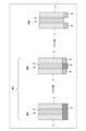
- 2A to 2C are process diagrams illustrating a method for manufacturing the semiconductor element according to the first embodiment.
- 2A to 2C are process diagrams illustrating a method for manufacturing the semiconductor element according to the first embodiment.
- 2A to 2C are process diagrams illustrating a method for manufacturing the semiconductor element according to the first embodiment.
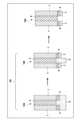
- 6A to 6C are process diagrams showing a method for manufacturing a semiconductor element according to a second embodiment.
- 6A to 6C are process diagrams showing a method for manufacturing a semiconductor element according to a second embodiment.
- 6A to 6C are process diagrams showing a method for manufacturing a semiconductor element according to a second embodiment.
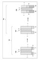
- 10A to 10C are process diagrams showing a method for manufacturing a semiconductor element according to a third embodiment.
- 10A to 10C are process diagrams showing a method for manufacturing a semiconductor element according to a third embodiment.
- 10A to 10C are process diagrams showing a method for manufacturing a semiconductor element according to a third embodiment.
- 2A to 2C are process diagrams illustrating a method for manufacturing the semiconductor element according to the first embodiment.
- 2A to 2C are process diagrams illustrating a method for manufacturing the semiconductor element according to the first embodiment.
- 2A to 2C are process diagrams illustrating a method for manufacturing the semiconductor element according to the first embodiment.
- 10A to 10C are process diagrams showing a method for manufacturing a semiconductor element according to a fourth embodiment.
- 10A to 10C are process diagrams showing a method for manufacturing a semiconductor element according to a fourth embodiment.
- 10A to 10C are process diagrams showing a method for manufacturing a semiconductor element according to a fourth embodiment.
- 10A to 10C are process diagrams showing a method for manufacturing a semiconductor element according to a fourth embodiment.
- 10A to 10C are process diagrams showing a method for manufacturing a semiconductor element according to a fourth embodiment.
- 10A to 10C are process diagrams showing a method for manufacturing a semiconductor element according to a fourth embodiment.
- 10A to 10C are process diagrams showing a method for manufacturing a semiconductor element according to a fourth embodiment.
- 10A to 10C are process diagrams showing a method for manufacturing a semiconductor element according to a fourth embodiment.
- 10A to 10C are process diagrams showing a method for manufacturing a semiconductor element according to a fourth embodiment.
- 13A to 13C are process diagrams showing a method for manufacturing a semiconductor element according to a fifth embodiment.
- 13A to 13C are process diagrams showing a method for manufacturing a semiconductor element according to a fifth embodiment.
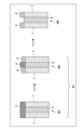
- 5A to 5C are diagrams showing a first embodiment of a method for manufacturing a semiconductor device, including a conversion process for converting amorphous silicon 1 into single crystal silicon 10.
- the inventor discovered that the Al film inhibits the silicidation of the Ni film from the results of an experiment in which an Al film and a Ni film are formed in sequence on amorphous silicon and a structure obtained by heating the structure was formed.
- NiAlSi has a lattice constant close to that of single crystal silicon, single crystal silicon can be easily obtained by contacting NiAlSi with amorphous silicon and performing heat treatment.
- the method for manufacturing a semiconductor device may include a conversion step of converting the amorphous silicon 1 into single crystal silicon 10.
- the amorphous silicon 1 may constitute a part of a substrate.
- the conversion step includes: A first step S1 of forming a first film 3 containing Ni (nickel) as a first material so as to cover the amorphous silicon 1 by a heat treatment involving heating, thereby forming Ni silicide as silicide 4 in contact with the amorphous silicon 1;
- a second step S2 is performed in which a second film 6 containing Al (aluminum) as a second material is formed to cover the silicide 4 by a treatment involving heating, thereby forming NiAlSi as a compound 7 composed of Si (silicon), Ni (first material), and Al (second material) in contact with the silicide 4;
- the method may include a third step S3 of converting the silicide 4 remaining after the second step S2 into a NiAlSi film as a
- FIG. 5A shows structure 101 at the stage where a first film 3 containing Ni as a first material is formed to cover amorphous silicon 1 by heat treatment involving heating in the first step S1, and structure 102 in which Ni silicide is formed as silicide 4.
- FIG. 5B shows structure 104 at the stage where a second film 6 containing Al as a second material is formed to cover silicide 4 by heat treatment, and structure 105 at the stage where NiAlSi as compound 7 composed of Si, Ni (first material), and Al (second material) is formed in contact with silicide 4.
- FIG. 5C shows structure 106 having silicide 4 remaining after second step S2, and structure 107 after silicide 4 is changed to compound 9 by heat treatment.
- the first material may be Pd (palladium), Ti (titanium), Cu (copper), Pt (platinum), Co (cobalt), Mo (molybdenum), Mg (magnesium), W (tungsten), Cr (chromium) or Mn (manganese).
- the first material may be one material selected from the group consisting of Ni, Pd, Ti, Cu, Pt, Co, Mo, Mg, W, Cr and Mn.
- the second material may be Au (gold), Sb (antimony), In (indium), Ag (silver) or Ga (gallium).
- the second material may be one material selected from the group consisting of Al, Au, Sb, In, Ag and Ga.
- the compound composed of Si, the first material, and the second material is preferably, for example, NiAlSi, NiAuSi, NiSbSi, NiInSi, NiAgSi, or NiGaSi.
- the conversion process of converting the amorphous silicon 1 into single crystal silicon 10 may further include a fourth step S4 in which at least a portion of the amorphous silicon 1 remaining after the third step S3 is converted into single crystal silicon 10 by heat treatment.
- FIG. 5C shows the structure 108 after at least a portion of the amorphous silicon 1 remaining after the third step S3 is converted into single crystal silicon 10 by heat treatment.
- the fourth step may include a Metal Induced Lateral Crystallization (MILC) process.
- MILC Metal Induced Lateral Crystallization
- the substrate on which the first step is performed may have an insulating film 2 (e.g., SiO 2 : silicon dioxide) in addition to the amorphous silicon 1.
- the amorphous silicon 1 and the insulating film 2 may be arranged in contact with each other or in close proximity to each other.
- a first film 3 containing a first material e.g., Ni
- FIG. 5A shows a structure 102 having a first material film 3′.
- the conversion process may further include a process of removing the first material film 3' in contact with the insulating film 2 by chemical etching or the like between the first step S1 and the second step S2.
- FIG. 5A shows a structure 103 from which the first material film 3' has been removed.
- the second material film 8 When the first material film 3' in contact with the insulating film 2 is removed, in the second step S2, when NiAlSi is formed as a compound 7 composed of Si, Ni (first material), and Al (second material) so as to be in contact with the silicide 4, the second material film 8, which is a part of the second film 6, remains in the portion covering the insulating film 2.
- the second material film 8 may be removed after the second step S2 (for example, between the second step S2 and the third step S3).
- the thickness T2 of the second film 6 formed in the second step S2 (the thickness of the second film 6 in the portion covering the Ni silicide 4) is preferably greater than the thickness T1 of the first film 3 formed in the first step S1 and smaller than four times the thickness T1 of the first film 3 formed in the first step S1. In other words, it is preferable to satisfy 0 ⁇ T2 ⁇ 4T1 .
- the lattice constant of NiSi 2-0 Al 0 i.e., NiSi 2
- the lattice constant of NiSi 1.46 Al 0.54 is 5.454.
- NiSi2-xAlx lattice constant 5.454 Therefore, since the lattice constant of NiSi2 is closer to that of Si (5.430) than that of NiSi2 (5.406), it is found to be suitable for forming single crystal silicon by the MILC process.
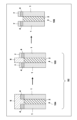
- FIGS. 6A to 6C are diagrams that show a second embodiment of a method for manufacturing a semiconductor device, including a conversion step for converting amorphous silicon 1 into single crystal silicon 10. Matters that are not mentioned in the second embodiment may follow the first embodiment.
- FIG. 6A shows the first step S1
- FIG. 6B shows the second step S2
- FIG. 6C shows the third step S3 and the fourth step S4.
- the first material film 3' in contact with the insulating film 2 is not removed between the first step S1 and the second step S2. Therefore, in the second step S2, a second film 6 containing Al as the second material is formed so as to cover the silicide 4 and the first material film 3' by a treatment involving heating, and in addition to the compound 7 in contact with the silicide 4, a second compound 11 of the first material and the second material is obtained so as to be in contact with the insulating film 2.
- the conversion process may include a process of removing the second compound 11 in contact with the insulating film 2 between the second process S2 and the third process S3.
- the second compound 11 By removing the second compound 11, it is possible to prevent the silicide 4 from growing laterally and combining with other silicides 4 to cause an electrical short circuit.
- FIG. 6B shows a structure 106 from which the second compound 11 has been removed.
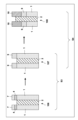
- FIGS. 7A to 7C are diagrams that show a third embodiment of a method for manufacturing a semiconductor device, including a conversion step for converting amorphous silicon into single crystal silicon. Matters not mentioned in the third embodiment may follow the first embodiment.
- FIG. 7A shows the first step S1
- FIG. 7B shows the second step S2
- FIG. 7C shows the third step S3 and the fourth step S4.
- the first material film 3' in contact with the insulating film 2 is not removed between the first step S1 and the second step S2. Therefore, in the second step S2, a second film 6 containing Al as the second material is formed so as to cover the silicide 4 and the first material film 3' by a process involving heating, and in addition to the compound 7 in contact with the silicide 4, a second compound 11 of the first material and the second material is obtained so as to be in contact with the insulating film 2. Also, in the second embodiment, the second compound 11 in contact with the insulating film 2 is not removed between the second step S2 and the third step S3.
- the conversion step may include a step of removing the second compound 11 in contact with the insulating film 2 after the third step S3, more specifically, between the third step S3 and the fourth step S4.
- removing the second compound 11 it is possible to prevent the silicide 4 from growing laterally and combining with other silicides 4 to cause an electrical short circuit.
- FIG. 7C shows a structure 107 from which the second compound 11 has been removed.
- the reference drawings show that the first and second films are formed on the amorphous silicon 1, but this merely shows that the first and second films are formed on the amorphous silicon 1 in the illustrated position.
- the formation of the first and second films on the amorphous silicon 1 does not limit the invention to the first and second films being formed above the amorphous silicon 1 in a film forming apparatus.
- the formation of the first and second films on the amorphous silicon 1 also includes the formation of the first and second films below the amorphous silicon 1 in a film forming apparatus, for example, as illustrated in Figures 8A to 8C.
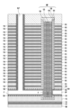
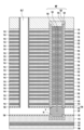
- the fourth embodiment provides a method for manufacturing a semiconductor memory device as an example of a semiconductor device.
- a semiconductor memory device having a NAND string will be described.
- the NAND string includes a plurality of thin film transistors connected in series.
- 100 denotes a semiconductor substrate
- 111, 114, 116, and 136 denote insulating films
- 112 and 113 denote wiring layers
- 115 denotes a gate electrode layer
- 119 denotes a tunnel insulating film
- 120 denotes a charge storage layer
- 121 denotes a block insulating film
- 135 denotes amorphous silicon
- 123 denotes a core layer
- 124A, 124B and 141 denote silicide layers
- 125 denotes a cap layer
- 136 denotes a conductive layer
- GP denotes a gap
- MP denotes a memory pillar
- SLT denotes a slit.
- the gap GP is connected to the external space via the slit SLT.
- the amorphous silicon 135 corresponds to the amorphous silicon 1 described above and is the target of single crystallization.
- the amorphous silicon 135 is exposed to the gap GP.
- a heat treatment involving heating is performed to form a first film 3 containing Ni as a first material so as to cover the amorphous silicon 135, thereby forming Ni silicide as the silicide 4 in contact with the amorphous silicon 135.
- a first material film 3' in contact with the insulating film can be formed.
- the first material film 3' can then be removed.
- a second film 6 containing Al as the second material is formed by a process involving heating so as to cover the silicide 4, thereby forming NiAlSi as a compound 7 composed of Si, Ni (first material), and Al (second material) so as to contact the silicide 4.
- a second material film 8 which is a part of the second film 6, remains in the portion covering the insulating film 136, etc.
- the second material film 8 on the insulating film is removed.
- the silicide film 4 remaining after the second step is transformed by heat treatment into a NiAlSi film as a compound 9 composed of Si, Ni (first material), and Al (second material).
- a fourth step shown in FIGS. 16 and 17 at least a part of the amorphous silicon 135 remaining after the third step is converted into single crystal silicon 10 by heat treatment.
- the fourth embodiment is advantageous in reducing channel resistance, which is an issue in semiconductor memory devices (for example, 3D NAND memories).
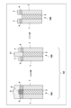
- FIGS. 18A and 18B are schematic diagrams showing a fifth embodiment of a method for manufacturing a semiconductor device, including a conversion step for converting amorphous silicon into single crystal silicon. Matters not mentioned in the fifth embodiment may follow the first to third embodiments. The fifth embodiment is also applicable to the fourth embodiment.
- the fifth embodiment of the method for manufacturing a semiconductor device may include a conversion step of converting amorphous silicon 1 into single crystal silicon 10.
- the amorphous silicon 1 may constitute a part of a substrate.
- the conversion step may include a first step S1' of forming a first film 3 containing Ni as a first material so as to cover the amorphous silicon 1, a second step S2' of forming a second film 6 containing Al as a second material so as to cover the first film 3 after the first step S1', and a third step S3' of changing the first film 3 into a NiAlSi film as a compound 9 composed of Si, Ni (first material), and Al (second material) by heat treatment after the second step S2'.
- the first material may be Pd (palladium), Ti (titanium), Cu (copper), Pt (platinum), Co (cobalt), Mo (molybdenum), Mg (magnesium), W (tungsten), Cr (chromium) or Mn (manganese).
- the first material may be one material selected from the group consisting of Ni, Pd, Ti, Cu, Pt, Co, Mo, Mg, W, Cr and Mn.
- the second material may be Au (gold), Sb (antimony), In (indium), Ag (silver) or Ga (gallium).
- the second material may be one material selected from the group consisting of Al, Au, Sb, In, Ag and Ga.
- the compound composed of Si (silicon), Ni (first material), and Al (second material) is preferably, for example, NiAlSi, NiAuSi, NiSbSi, NiInSi, NiAgSi, or NiGaSi.
- the conversion process for converting the amorphous silicon 1 into single crystal silicon 10 may further include a fourth process S4' in which at least a portion of the amorphous silicon 1 remaining after the third process S3' is converted into single crystal silicon 10 by heat treatment.
- the conversion process may also include a process for removing the second compound 11 in contact with the insulating film 2 between the third process S3' and the fourth process S4'.
- the fourth step S4' a laminated structure of amorphous silicon 1, compound 9, and single crystal silicon 10 is formed.
- the fourth step S4' may include a MILC (Metal Induced Lateral Crystallization) process. It is preferable that the thickness of the second film 6 formed in the second step S2' is greater than the thickness of the first film 3 formed in the first step S1' and is less than four times the thickness of the first film 3 formed in the first step S1'.
- 1 amorphous silicon
- 2 insulating film
- 3 first film (e.g. Ni film), 3': first material film (e.g. Ni film)
- 4 silicide (e.g. Ni silicide)
- 6 second film (e.g. Al film)
- 7 compound (e.g. NiAlSi)
- 8 second material film (e.g. Al film)
- 9 compound (e.g. NiAlSi)
- 10 single crystal silicon
- 11 second compound (e.g. NiAl)
Landscapes
- Electrodes Of Semiconductors (AREA)
- Chemical & Material Sciences (AREA)
- Crystallography & Structural Chemistry (AREA)
- Recrystallisation Techniques (AREA)
- Non-Volatile Memory (AREA)
Abstract
Description
加熱を伴う熱処理により、アモルファスシリコン1を覆うように第1材料としてのNi(ニッケル)を含む第1膜3を形成することにより、アモルファスシリコン1に接するシリサイド4としてのNiシリサイドを形成する第1工程S1と、
第1工程S1の後、加熱を伴う処理により、シリサイド4を覆うように第2材料としてのAl(アルミニウム)を含む第2膜6を形成することにより、シリサイド4に接するように、Si(シリコン)、Ni(第1材料)、Al(第2材料)で構成される化合物7としてのNiAlSiを形成する第2工程S2と、
第2工程S2の後に残っているシリサイド4を、熱処理により、Si、Ni(第1材料)、Al(第2材料)で構成される化合物9としてのNiAlSi膜に変化させる第3工程S3と、を含みうる。
よって、NiSi2の格子定数(5.406)に比べて、Siの格子定数=5.430に近いため、MILCプロセスによる単結晶シリコンの形成に適していることが分かる。
第4実施形態は、半導体記憶装置(例えば、3D NANDメモリ)の課題であるチャネル抵抗の低減に有利である。
Claims (28)
- アモルファスシリコンを単結晶シリコンに変換する変換工程を含む、半導体素子の製造方法において、前記変換工程は、
加熱を伴う処理により、前記アモルファスシリコンを覆うように第1材料を含む第1膜を形成することにより、前記アモルファスシリコンに接するシリサイドを形成する第1工程と、
前記第1工程後、加熱を伴う処理により、前記シリサイドを覆うように第2材料を含む第2膜を形成することにより、前記シリサイドに接するように、Si、前記第1材料および前記第2材料で構成される化合物を形成する第2工程と、
前記第2工程後に残っている前記シリサイドを、熱処理により、前記化合物に変化させる第3工程と、を含み、
前記第1材料は、Ni、Pd、Ti、Cu、Pt、Co、Mo、Mg、W、CrおよびMnからなるグループから選択される1つの材料であり、
前記第2材料は、Al、Au、Sb、In、AgおよびGaからなるグループから選択される1つの材料である、
ことを特徴とする半導体素子の製造方法。 - 前記変換工程は、前記第3工程後に残っている前記アモルファスシリコンの少なくとも一部を、熱処理により、単結晶シリコンに変化させる第4工程を更に含む、
ことを特徴とする請求項1に記載の半導体素子の製造方法。 - 前記第4工程を経て、前記アモルファスシリコン、前記化合物および前記単結晶シリコンの積層構造が形成される、
ことを特徴とする請求項2に記載の半導体素子の製造方法。 - 前記第4工程は、MILC(Metal Induced Lateral Crystallization)プロセスを含む、
ことを特徴とする請求項3に記載の半導体素子の製造方法。 - 前記第2工程で形成する前記第2膜の厚さは、前記第1工程で形成される前記第1膜の厚さより大きく、前記第1工程で形成される前記第1膜の厚さの4倍より小さい、
ことを特徴とする、請求項1乃至4のいずれか1項に記載の半導体素子の製造方法。 - 前記第2材料は、Alである、
ことを特徴とする請求項1乃至5のいずれか1項に記載の半導体素子の製造方法。 - 前記第1材料は、Niである、
ことを特徴とする請求項1乃至5のいずれか1項に記載の半導体素子の製造方法。 - 前記第1材料は、Niであり、前記第2材料は、Alである、
ことを特徴とする請求項1乃至5のいずれか1項に記載の半導体素子の製造方法。 - 前記第1工程では、加熱を伴う処理により、前記アモルファスシリコンの他、絶縁膜を覆うように前記第1材料を含む前記第1膜を形成することにより、前記アモルファスシリコンに接する前記シリサイドの他、前記絶縁膜に接する第1材料膜が形成される、
ことを特徴とする請求項1から4のいずれか1項に記載の半導体素子の製造方法。 - 前記変換工程は、前記第1工程と前記第2工程との間に、前記絶縁膜に接する前記第1材料膜を除去する工程を更に含む、
ことを特徴とする請求項9に記載の半導体素子の製造方法。 - 前記第2工程では、加熱を伴う処理により、前記シリサイドの他、前記絶縁膜を覆うように前記第1材料を含む前記第2膜を形成することにより、前記シリサイドに接する前記化合物の他、前記絶縁膜に接する第2材料膜が形成される、
ことを特徴とする請求項10に記載の半導体素子の製造方法。 - 前記変換工程は、前記第2工程と前記第3工程との間に、前記絶縁膜に接する前記第2材料膜を除去する工程を更に含む、
ことを特徴とする請求項11に記載の半導体素子の製造方法。 - 前記第2工程では、加熱を伴う処理により、前記シリサイドおよび前記第1材料膜を覆うように第2材料を含む前記第2膜を形成することにより、前記シリサイドに接する前記化合物の他、前記絶縁膜に接する、前記第1材料および前記第2材料の第2化合物が得られる、
ことを特徴とする請求項9に記載の半導体素子の製造方法。 - 前記変換工程は、前記第2工程と前記第3工程との間に、前記絶縁膜に接する前記第2化合物を除去する工程を含む、
ことを特徴とする請求項13に記載の半導体素子の製造方法。 - 前記変換工程は、前記第3工程の後に、前記絶縁膜に接する前記第2化合物を除去する工程を更に含む、
ことを特徴とする請求項13に記載の半導体素子の製造方法。 - 請求項1乃至15のいずれか1項に記載の半導体素子の製造方法により作成された単結晶シリコンを含む半導体素子。
- 前記単結晶シリコンが薄膜トランジスター又は半導体記憶装置の一部を構成することを特徴とする請求項16に記載の半導体素子。
- アモルファスシリコンを単結晶シリコンに変換する変換工程を含む、半導体素子の製造方法において、前記変換工程は、
前記アモルファスシリコンを覆うように第1材料を含む第1膜を形成する第1工程と、
前記第1工程後、前記第1膜を覆うように第2材料を含む第2膜を形成する第2工程と、
前記第2工程後、熱処理により、Si、前記第1材料および前記第2材料を含む化合物を形成する第3工程と、を含み、
前記第1材料は、Ni、Pd、Ti、Cu、Pt、Co、Mo、Mg、W、CrおよびMnからなるグループから選択される1つの材料であり、
前記第2材料は、Al、Au、Sb、In、AgおよびGaからなるグループから選択される1つの材料である、
ことを特徴とする半導体素子の製造方法。 - 前記変換工程は、前記第3工程後に残っている前記アモルファスシリコンの少なくとも一部を、熱処理により、単結晶シリコンに変化させる第4工程を更に含む、
ことを特徴とする請求項18に記載の半導体素子の製造方法。 - 前記第4工程を経て、前記アモルファスシリコン、前記化合物および前記単結晶シリコンの積層構造が形成される、
ことを特徴とする請求項19に記載の半導体素子の製造方法。 - 前記第4工程は、MILC(Metal Induced Lateral Crystallization)プロセスを含む、
ことを特徴とする請求項20に記載の半導体素子の製造方法。 - 前記第2工程で形成する前記第2膜の厚さは、前記第1工程で形成される前記第1膜の厚さより大きく、前記第1工程で形成される前記第1膜の厚さの4倍より小さい、
ことを特徴とする、請求項18乃至21のいずれか1項に記載の半導体素子の製造方法。 - 前記第2材料は、Alである、
ことを特徴とする請求項18乃至22のいずれか1項に記載の半導体素子の製造方法。 - 前記第1材料は、Niである、
ことを特徴とする請求項18乃至22のいずれか1項に記載の半導体素子の製造方法。 - 前記第1材料は、Niであり、前記第2材料は、Alである、
ことを特徴とする請求項18乃至22のいずれか1項に記載の半導体素子の製造方法。 - 請求項18乃至25のいずれか1項に記載の半導体素子の製造方法により作成された単結晶シリコンを含む半導体素子。
- 前記単結晶シリコンが薄膜トランジスター又は半導体記憶装置の一部を構成することを特徴とする請求項26に記載の半導体素子。
- アモルファスシリコン、化合物および単結晶シリコンの積層構造を含む半導体素子であって、
前記化合物は、Si、第1材料および第2材料の化合物であり、
前記第1材料は、Ni、Pd、Ti、Cu、Pt、Co、Mo、Mg、W、CrおよびMnからなるグループから選択される1つの材料であり、
前記第2材料は、Al、Au、Sb、In、AgおよびGaからなるグループから選択される1つの材料である、
ことを特徴とする半導体素子。
Priority Applications (7)
| Application Number | Priority Date | Filing Date | Title |
|---|---|---|---|
| KR1020247028711A KR102835288B1 (ko) | 2023-07-14 | 2024-04-08 | 반도체 소자의 제조 방법 및 반도체 소자 |
| CN202480002783.9A CN119654979A (zh) | 2023-07-14 | 2024-04-08 | 半导体器件制造方法及半导体器件 |
| JP2024554238A JP7659708B1 (ja) | 2023-07-14 | 2024-04-08 | 半導体素子の製造方法及び半導体素子 |
| KR1020257023267A KR102936129B1 (ko) | 2023-07-14 | 2024-04-08 | 반도체 소자의 제조 방법 및 반도체 소자 |
| EP24798710.0A EP4521878A4 (en) | 2023-07-14 | 2024-04-08 | METHOD FOR MANUFACTURING SEMICONDUCTOR ELEMENTS AND SEMICONDUCTOR ELEMENTS |
| TW113115473A TWI910617B (zh) | 2023-07-14 | 2024-04-25 | 半導體元件之製造方法及半導體元件 |
| US18/943,526 US20250081500A1 (en) | 2023-07-14 | 2024-11-11 | Method of manufacturing semiconductor device and semiconductor device |
Applications Claiming Priority (2)
| Application Number | Priority Date | Filing Date | Title |
|---|---|---|---|
| JP2023115732 | 2023-07-14 | ||
| JP2023-115732 | 2023-07-14 |
Related Child Applications (1)
| Application Number | Title | Priority Date | Filing Date |
|---|---|---|---|
| US18/943,526 Continuation US20250081500A1 (en) | 2023-07-14 | 2024-11-11 | Method of manufacturing semiconductor device and semiconductor device |
Publications (1)
| Publication Number | Publication Date |
|---|---|
| WO2025017981A1 true WO2025017981A1 (ja) | 2025-01-23 |
Family
ID=94281866
Family Applications (1)
| Application Number | Title | Priority Date | Filing Date |
|---|---|---|---|
| PCT/JP2024/014280 Pending WO2025017981A1 (ja) | 2023-07-14 | 2024-04-08 | 半導体素子の製造方法及び半導体素子 |
Country Status (7)
| Country | Link |
|---|---|
| US (1) | US20250081500A1 (ja) |
| EP (1) | EP4521878A4 (ja) |
| JP (1) | JP7659708B1 (ja) |
| KR (2) | KR102936129B1 (ja) |
| CN (1) | CN119654979A (ja) |
| TW (1) | TWI910617B (ja) |
| WO (1) | WO2025017981A1 (ja) |
Families Citing this family (1)
| Publication number | Priority date | Publication date | Assignee | Title |
|---|---|---|---|---|
| CN120711792B (zh) * | 2025-08-12 | 2025-12-16 | 合肥晶合集成电路股份有限公司 | 半导体器件及其制造方法 |
Citations (6)
| Publication number | Priority date | Publication date | Assignee | Title |
|---|---|---|---|---|
| JP2005159307A (ja) | 2003-11-22 | 2005-06-16 | Samsung Sdi Co Ltd | 金属誘導側面結晶化方法を用いた薄膜トランジスター及びその製造方法 |
| JP2007251030A (ja) * | 2006-03-17 | 2007-09-27 | Renesas Technology Corp | 半導体装置の製造方法および半導体装置 |
| JP2014175348A (ja) | 2013-03-06 | 2014-09-22 | Toshiba Corp | 不揮発性半導体記憶装置 |
| JP2018157069A (ja) * | 2017-03-17 | 2018-10-04 | 東芝メモリ株式会社 | 半導体記憶装置 |
| JP2019165178A (ja) | 2018-03-20 | 2019-09-26 | 東芝メモリ株式会社 | 半導体記憶装置 |
| US20200083238A1 (en) * | 2015-11-16 | 2020-03-12 | Micron Technology, Inc. | Integrated Structures and Methods of Forming Integrated Structures |
Family Cites Families (13)
| Publication number | Priority date | Publication date | Assignee | Title |
|---|---|---|---|---|
| KR100390523B1 (ko) * | 2001-01-20 | 2003-07-04 | 주승기 | 실리콘 박막 결정화 방법 |
| KR100623228B1 (ko) * | 2003-11-27 | 2006-09-18 | 삼성에스디아이 주식회사 | 박막트랜지스터, 상기 박막트랜지스터를 구비하는유기전계발광표시장치 및 상기 박막트랜지스터의 제조방법 |
| TWI392092B (zh) * | 2008-11-10 | 2013-04-01 | 國立中山大學 | 具π型半導體導通層之半導體裝置及其製造方法 |
| CN102709184B (zh) * | 2011-05-13 | 2016-08-17 | 京东方科技集团股份有限公司 | 含有多晶硅有源层的薄膜晶体管、其制造方法及阵列基板 |
| JP2014179465A (ja) * | 2013-03-14 | 2014-09-25 | Toshiba Corp | 不揮発性半導体記憶装置およびその製造方法 |
| CN105244414B (zh) * | 2015-10-20 | 2017-04-12 | 华中科技大学 | 一种二硫化钼/ 硅异质结太阳能电池及其制备方法 |
| JP2017174860A (ja) * | 2016-03-18 | 2017-09-28 | 東芝メモリ株式会社 | 半導体記憶装置及びその製造方法 |
| CN108022934A (zh) * | 2016-11-01 | 2018-05-11 | 沈阳硅基科技有限公司 | 一种薄膜的制备方法 |
| KR102403102B1 (ko) * | 2016-12-15 | 2022-05-26 | 에이에스엠 아이피 홀딩 비.브이. | 반도체 처리 장치 |
| JP7371507B2 (ja) * | 2020-01-22 | 2023-10-31 | 富士電機株式会社 | 炭化珪素半導体装置の製造方法 |
| FR3106932B1 (fr) * | 2020-02-04 | 2023-10-27 | Commissariat Energie Atomique | Procede de fabrication d’un substrat structure |
| CN112786614B (zh) | 2021-03-22 | 2022-04-29 | 长江存储科技有限责任公司 | 制备三维存储器的方法 |
| CN115548140A (zh) * | 2022-10-20 | 2022-12-30 | 中建材浚鑫科技有限公司 | 一种金属化异质结电池及其制备方法 |
-
2024
- 2024-04-08 KR KR1020257023267A patent/KR102936129B1/ko active Active
- 2024-04-08 EP EP24798710.0A patent/EP4521878A4/en active Pending
- 2024-04-08 WO PCT/JP2024/014280 patent/WO2025017981A1/ja active Pending
- 2024-04-08 KR KR1020247028711A patent/KR102835288B1/ko active Active
- 2024-04-08 JP JP2024554238A patent/JP7659708B1/ja active Active
- 2024-04-08 CN CN202480002783.9A patent/CN119654979A/zh active Pending
- 2024-04-25 TW TW113115473A patent/TWI910617B/zh active
- 2024-11-11 US US18/943,526 patent/US20250081500A1/en active Pending
Patent Citations (6)
| Publication number | Priority date | Publication date | Assignee | Title |
|---|---|---|---|---|
| JP2005159307A (ja) | 2003-11-22 | 2005-06-16 | Samsung Sdi Co Ltd | 金属誘導側面結晶化方法を用いた薄膜トランジスター及びその製造方法 |
| JP2007251030A (ja) * | 2006-03-17 | 2007-09-27 | Renesas Technology Corp | 半導体装置の製造方法および半導体装置 |
| JP2014175348A (ja) | 2013-03-06 | 2014-09-22 | Toshiba Corp | 不揮発性半導体記憶装置 |
| US20200083238A1 (en) * | 2015-11-16 | 2020-03-12 | Micron Technology, Inc. | Integrated Structures and Methods of Forming Integrated Structures |
| JP2018157069A (ja) * | 2017-03-17 | 2018-10-04 | 東芝メモリ株式会社 | 半導体記憶装置 |
| JP2019165178A (ja) | 2018-03-20 | 2019-09-26 | 東芝メモリ株式会社 | 半導体記憶装置 |
Non-Patent Citations (2)
| Title |
|---|
| KLAUS ET AL., APPL. PHYS. LETT, vol. 83, no. 497, 2003, pages 497 - 499 |
| See also references of EP4521878A4 |
Also Published As
| Publication number | Publication date |
|---|---|
| KR20250111390A (ko) | 2025-07-22 |
| JP7659708B1 (ja) | 2025-04-09 |
| KR102936129B1 (ko) | 2026-03-09 |
| KR20250013142A (ko) | 2025-01-31 |
| JPWO2025017981A1 (ja) | 2025-01-23 |
| TW202519029A (zh) | 2025-05-01 |
| EP4521878A1 (en) | 2025-03-12 |
| KR102835288B1 (ko) | 2025-07-18 |
| CN119654979A (zh) | 2025-03-18 |
| US20250081500A1 (en) | 2025-03-06 |
| EP4521878A4 (en) | 2026-04-29 |
| TWI910617B (zh) | 2026-01-01 |
Similar Documents
| Publication | Publication Date | Title |
|---|---|---|
| KR100611766B1 (ko) | 박막트랜지스터 제조 방법 | |
| JP5091017B2 (ja) | 薄膜トランジスタの製造方法 | |
| KR101084233B1 (ko) | 박막트랜지스터 및 그 제조 방법 | |
| JP2009004770A (ja) | 多結晶シリコン層の製造方法、これを用いて形成した薄膜トランジスタ、その製造方法、並びに、これを備えた有機電界発光表示装置 | |
| JP5497324B2 (ja) | 多結晶シリコンの製造方法、薄膜トランジスタ、その製造方法及びそれを含む有機電界発光表示装置 | |
| JP2010206200A (ja) | 有機電界発光表示装置及びその製造方法 | |
| US20060030085A1 (en) | Method of fabricating thin film transistor | |
| US9406730B2 (en) | Thin film transistor and organic light emitting device including polycrystalline silicon layer | |
| JP5433462B2 (ja) | 半導体装置の製造方法 | |
| JP2010206196A (ja) | 薄膜トランジスタ、その製造方法及びそれを含む有機電界発光表示装置 | |
| JP7659708B1 (ja) | 半導体素子の製造方法及び半導体素子 | |
| US8890165B2 (en) | Method of forming polycrystalline silicon layer, thin film transistor, organic light emitting diode display device having the same, and methods of fabricating the same | |
| JP2009060009A (ja) | 結晶質半導体膜の製造方法およびアクティブマトリクス基板の製造方法 | |
| KR100611761B1 (ko) | 박막트랜지스터 제조 방법 | |
| CN1716532B (zh) | 制备显示装置的方法 | |
| JP5380305B2 (ja) | 半導体素子の製造方法 | |
| CN100536075C (zh) | 制造薄膜晶体管的方法 | |
| KR100369340B1 (ko) | 티타늄실리사이드의 형성 방법 | |
| JPH08148425A (ja) | 半導体装置およびその製造方法 | |
| JPH0864828A (ja) | 薄膜トランジスタの製造方法 | |
| US7256080B2 (en) | Method of fabricating thin film transistor | |
| US20230352296A1 (en) | Structure and formation method of device with ferroelectric layer | |
| KR100861796B1 (ko) | 반도체 소자의 배선 형성 방법 | |
| TW200839959A (en) | Method for fabricating semiconductor device | |
| TW201901755A (zh) | 多晶半導體薄膜、薄膜電晶體及其製造方法 |
Legal Events
| Date | Code | Title | Description |
|---|---|---|---|
| WWE | Wipo information: entry into national phase |
Ref document number: 2024554238 Country of ref document: JP |
|
| WWE | Wipo information: entry into national phase |
Ref document number: 202480002783.9 Country of ref document: CN |
|
| ENP | Entry into the national phase |
Ref document number: 2024798710 Country of ref document: EP Effective date: 20241106 |
|
| WWP | Wipo information: published in national office |
Ref document number: 202480002783.9 Country of ref document: CN |
|
| WWD | Wipo information: divisional of initial pct application |
Ref document number: 1020257023267 Country of ref document: KR |
|
| WWP | Wipo information: published in national office |
Ref document number: 1020257023267 Country of ref document: KR |
|
| NENP | Non-entry into the national phase |
Ref country code: DE |