WO2025028005A1 - Élément de capteur infrarouge, capteur infrarouge et système de détection de position - Google Patents
Élément de capteur infrarouge, capteur infrarouge et système de détection de position Download PDFInfo
- Publication number
- WO2025028005A1 WO2025028005A1 PCT/JP2024/020176 JP2024020176W WO2025028005A1 WO 2025028005 A1 WO2025028005 A1 WO 2025028005A1 JP 2024020176 W JP2024020176 W JP 2024020176W WO 2025028005 A1 WO2025028005 A1 WO 2025028005A1
- Authority
- WO
- WIPO (PCT)
- Prior art keywords
- infrared sensor
- side electrode
- principal surface
- thickness direction
- outer edge
- Prior art date
- Legal status (The legal status is an assumption and is not a legal conclusion. Google has not performed a legal analysis and makes no representation as to the accuracy of the status listed.)
- Pending
Links
Images


Classifications
-
- G—PHYSICS
- G01—MEASURING; TESTING
- G01J—MEASUREMENT OF INTENSITY, VELOCITY, SPECTRAL CONTENT, POLARISATION, PHASE OR PULSE CHARACTERISTICS OF INFRARED, VISIBLE OR ULTRAVIOLET LIGHT; COLORIMETRY; RADIATION PYROMETRY
- G01J5/00—Radiation pyrometry, e.g. infrared or optical thermometry
- G01J5/10—Radiation pyrometry, e.g. infrared or optical thermometry using electric radiation detectors
-
- G—PHYSICS
- G01—MEASURING; TESTING
- G01J—MEASUREMENT OF INTENSITY, VELOCITY, SPECTRAL CONTENT, POLARISATION, PHASE OR PULSE CHARACTERISTICS OF INFRARED, VISIBLE OR ULTRAVIOLET LIGHT; COLORIMETRY; RADIATION PYROMETRY
- G01J1/00—Photometry, e.g. photographic exposure meter
- G01J1/02—Details
-
- G—PHYSICS
- G01—MEASURING; TESTING
- G01J—MEASUREMENT OF INTENSITY, VELOCITY, SPECTRAL CONTENT, POLARISATION, PHASE OR PULSE CHARACTERISTICS OF INFRARED, VISIBLE OR ULTRAVIOLET LIGHT; COLORIMETRY; RADIATION PYROMETRY
- G01J5/00—Radiation pyrometry, e.g. infrared or optical thermometry
- G01J5/02—Constructional details
- G01J5/08—Optical arrangements
- G01J5/0806—Focusing or collimating elements, e.g. lenses or concave mirrors
-
- G—PHYSICS
- G01—MEASURING; TESTING
- G01J—MEASUREMENT OF INTENSITY, VELOCITY, SPECTRAL CONTENT, POLARISATION, PHASE OR PULSE CHARACTERISTICS OF INFRARED, VISIBLE OR ULTRAVIOLET LIGHT; COLORIMETRY; RADIATION PYROMETRY
- G01J5/00—Radiation pyrometry, e.g. infrared or optical thermometry
- G01J5/02—Constructional details
- G01J5/08—Optical arrangements
- G01J5/084—Adjustable or slidable
-
- G—PHYSICS
- G01—MEASURING; TESTING
- G01V—GEOPHYSICS; GRAVITATIONAL MEASUREMENTS; DETECTING MASSES OR OBJECTS; TAGS
- G01V8/00—Prospecting or detecting by optical means
- G01V8/10—Detecting, e.g. by using light barriers
-
- G—PHYSICS
- G01—MEASURING; TESTING
- G01J—MEASUREMENT OF INTENSITY, VELOCITY, SPECTRAL CONTENT, POLARISATION, PHASE OR PULSE CHARACTERISTICS OF INFRARED, VISIBLE OR ULTRAVIOLET LIGHT; COLORIMETRY; RADIATION PYROMETRY
- G01J5/00—Radiation pyrometry, e.g. infrared or optical thermometry
- G01J5/10—Radiation pyrometry, e.g. infrared or optical thermometry using electric radiation detectors
- G01J2005/106—Arrays
Definitions
- the present disclosure relates to an infrared sensor element, an infrared sensor including the infrared sensor element, and a position detection system including the infrared sensor.
- Infrared sensors that use pyroelectric elements are known (see, for example, Patent Document 1). Such infrared sensors are used, for example, to detect the presence of a detection target such as a human body.
- infrared light emitted from the object to be detected passes through a lens and is focused on the pyroelectric element, forming an image on the pyroelectric element.
- the part of the pyroelectric element that is irradiated with infrared light is heated, causing a change in temperature of that part.
- an electric charge is generated on the surface of that part of the pyroelectric element due to the pyroelectric effect. This charge is output as an electrical signal outside the pyroelectric element.
- the object to be detected is detected based on the output electrical signal.
- the size and amount of light of the image focused on the pyroelectric element In order for a temperature change to occur in the pyroelectric element, the size and amount of light of the image focused on the pyroelectric element must change. When detecting a moving object, the size and amount of light of the image focused on a stationary pyroelectric element may change. On the other hand, in order to detect a stationary object, for example, the pyroelectric element is moved to change the image focused on the pyroelectric element.
- Patent document 2 discloses an infrared sensor that changes the distance between a pyroelectric element and an object to be detected by vibrating the pyroelectric element in the direction of the optical axis of the light receiving surface of the pyroelectric element.
- Patent No. 4702366 Japanese Patent Application Publication No. 8-184492
- the objective of this disclosure is to provide an infrared sensor element that can be miniaturized while still being able to detect the direction in which an object to be detected is located.
- the infrared sensor element includes: a pyroelectric element having one main surface facing one side in a thickness direction and another main surface overlapping the one main surface when viewed from the thickness direction and facing the other side in the thickness direction; A first electrode provided on the first principal surface; a second-side electrode provided on the second principal surface and overlapping the first-side electrode when viewed in the thickness direction, When viewed from the thickness direction, the one electrode or the other electrode has a curved outer edge portion that is parabolic.
- This disclosure makes it possible to provide an infrared sensor element that can be miniaturized while still being able to detect the direction in which an object to be detected is located.
- FIG. 1 is a flowchart for explaining the operation of the position detection system.
- FIG. 1 is a schematic plan view of an infrared sensor element for explaining calculation of the image center position; FIG.
- FIG. 4 is a schematic cross-sectional view corresponding to the cross-section B-B of FIG. 3, showing a modified example of the infrared sensor element and the support portion;
- Schematic plan view of a modified example of the infrared sensor element Schematic plan view of a modified example of the infrared sensor element
- FIG. 12 is a schematic cross-sectional view corresponding to the CC cross section of FIG. 11, showing a modified example of the infrared sensor element and the support portion.
- FIG. 12 is a schematic cross-sectional view showing the cross section DD of FIG.
- FIG. 12 is a schematic cross-sectional view showing the cross section DD of FIG.
- FIG. 12 is a schematic cross-sectional view corresponding to the CC cross section of FIG. 11, showing a modified example of the infrared sensor element and the support portion. Schematic diagram showing infrared irradiation from a detection target to two infrared sensors
- FIG. 1 is a functional block diagram of a position detection system according to a first embodiment of the present disclosure
- Fig. 2 is a schematic diagram showing irradiation of infrared rays from a detection target to an infrared sensor.
- the position detection system 1 includes an infrared sensor 2 and a lens 6.
- the infrared sensor 2 outputs an electrical signal based on infrared rays 7A emitted from a detection target 7 (see FIG. 2), such as a person.
- a detection target 7 see FIG. 2
- the infrared rays 7A are indicated by dashed arrows in FIG. 2 and in FIG. 17, which will be described later.
- the infrared sensor 2 includes an infrared sensor element 4, a drive unit 5, and a control unit 3. As described below, the control unit 3 controls the drive unit 5, receives a signal from the infrared sensor element 4, and calculates the image center position k (see Fig. 2).
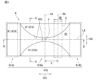
- FIG. 3 is a schematic plan view of the infrared sensor element.
- FIG. 4 is a schematic bottom view of the infrared sensor element.
- FIG. 5 is a schematic cross-sectional view showing the A-A cross section of FIG. 3.
- the infrared sensor element 4 includes a pyroelectric element 41, and a first electrode 42 and a second electrode 43 stacked on the pyroelectric element 41 in the thickness direction 101. Note that the first electrode 42 and the second electrode 43 are not shown in Figure 2.
- the pyroelectric element 41 has a rectangular parallelepiped shape. As shown in Figures 3 and 4, the pyroelectric element 41 has one rectangular main surface 41A and the other rectangular main surface 41B. As shown in Figure 5, the one main surface 41A faces one side in the thickness direction 101. The other main surface 41B faces the other side in the thickness direction 101. When viewed from the thickness direction 101, the one main surface 41A and the other main surface 41B overlap. Note that the pyroelectric element 41 is not limited to a rectangular parallelepiped. For example, the pyroelectric element 41 may be cylindrical.
- the one-side electrode 42 is laminated on one main surface 41A of the pyroelectric element 41. In other words, the one-side electrode 42 is provided on one main surface 41A.
- the other-side electrode 43 is laminated on the other main surface 41B of the pyroelectric element 41. In other words, the other-side electrode 43 is provided on the other main surface 41B.
- one principal surface 41A of the pyroelectric element 41 has a detection area 41Aa and two non-detection areas 41Ab, 41Ac.
- the two non-detection areas 41Ab, 41Ac are provided on both sides of the one principal surface 41A in the X-axis direction 103.
- the detection area 41Aa is provided between the two non-detection areas 41Ab, 41Ac in the X-axis direction 103.
- the X-axis direction 103 is parallel to the one principal surface 41A and is parallel to the longitudinal direction of the rectangular one principal surface 41A.
- the other main surface 41B of the pyroelectric element 41 has a detection area 41Ba and two non-detection areas 41Bb, 41Bc.
- the two non-detection areas 41Bb, 41Bc are provided on both sides of the other main surface 41B in the X-axis direction 103.
- the detection area 41Ba is provided between the two non-detection areas 41Bb, 41Bc in the X-axis direction 103.
- the detection areas 41Aa, 41Ba shown in Figures 3 and 4 are areas where infrared rays 7A (see Figure 3) from the detection object 7 are irradiated and an image 8 is formed.
- the non-detection areas 41Ab, 41Ac, 41Bb, and 41Bc are areas used for electrical connection of the infrared sensor element 4 to the outside and for supporting the pyroelectric element 41.
- non-detection areas 41Ab, 41Ac, 41Bb, and 41Bc are areas surrounded by dashed lines
- detection areas 41Aa and 41Ba are areas excluding the areas surrounded by dashed lines.
- the detection area 41Aa of one main surface 41A overlaps with the detection area 41Ba of the other main surface 41B.
- the non-detection area 41Ab of one main surface 41A overlaps with the non-detection area 41Bb of the other main surface 41B.
- the non-detection area 41Ac of one main surface 41A overlaps with the non-detection area 41Bc of the other main surface 41B.
- the entire area of the detection area 41Aa overlaps with the entire area of the detection area 41Ba when viewed from the thickness direction 101, but this is not limited to the configuration.
- a portion of the detection area 41Aa may overlap a portion of the detection area 41Ba when viewed from the thickness direction 101.
- non-detection region 41Ab when viewed from the thickness direction 101, overlaps with the entire area of non-detection region 41Bb, and the entire area of non-detection region 41Ac overlaps with the entire area of non-detection region 41Bc, but this is not limited to the configuration.
- non-detection region 41Ab when viewed from the thickness direction 101, does not have to overlap with non-detection region 41Bb.
- the one-side electrode 42 is provided across the detection area 41Aa and the non-detection area 41Ab of the one main surface 41A.
- the other electrode 43 is provided across the detection area 41Ba and the non-detection area 41Bc of the other main surface 41B.
- the portion of the one-side electrode 42 provided in the detection region 41Aa overlaps with the portion of the other-side electrode 43 provided in the detection region 41Ba.
- the portion of the one-side electrode 42 provided in the non-detection region 41Ab does not overlap with the portion of the other-side electrode 43 provided in the non-detection region 41Bc.
- the non-detection region 41Ab of the one main surface 41A on which the one-side electrode 42 is provided is located outside the non-detection region 41Bc of the other main surface 41B on which the other-side electrode 43 is provided.
- the non-detection area of the first main surface 41A on which the first electrode 42 is provided may overlap with the non-detection area of the second main surface 41B on which the second electrode 43 is provided.
- the first electrode 42 may be provided in the non-detection area 41Ac of the first main surface 41A
- the second electrode 43 may be provided in the non-detection area 41Bc of the second main surface 41B.
- the one-side electrode 42 has two curved outer edge portions 42A that are parabolic. Each parabola of the two curved outer edge portions 42A has a common axis AX.
- the axis AX is parallel to the Y-axis direction 104.
- the Y-axis direction 104 is a direction parallel to the short side direction of the rectangular one main surface 41A. In other words, the Y-axis direction 104 is a direction parallel to the one main surface 41A and perpendicular to the X-axis direction 103.
- the two curved outer edge portions 42A are line-symmetrical with respect to a straight line LN perpendicular to the axis AX, that is, with respect to a straight line LN parallel to the X-axis direction 103, so that the vertices of the two curved outer edge portions 42A are closest to each other. Note that the two curved outer edge portions 42A do not have to be line-symmetrical with each other.
- FIG. 6 is a schematic cross-sectional view corresponding to the B-B cross section in FIG. 3, showing the infrared sensor element and the support part.
- the infrared sensor element 4 is supported by a support portion 91.
- the support portion 91 is made of LTCC (Low Temperature Co-fired Ceramics) and has a first support portion 911 and a second support portion 912 laminated on the first support portion 911. Note that the boundary between the first support portion 911 and the second support portion 912 may be indistinguishable. Therefore, in FIG. 6, the boundary is shown by a dashed line.
- the support portion 91 may be made of a material other than LTCC.
- Conductive pastes 921, 922 made of copper or the like are formed on the first support portion 911.
- the pyroelectric element 41 is attached on the pastes 921, 922 with the other principal surface 41B facing the pastes 921, 922.
- the other side electrode 43 formed on the other principal surface 41B is in contact with the paste 922.
- Conductive pastes 931 and 932 made of copper or the like are formed on the second support portion 912.
- Paste 931 is in contact with paste 921 and one-side electrode 42.
- Paste 932 is in contact with paste 922.
- Wiring 94, 95 are formed on the surface and inside of support portion 91.
- Wiring 94 is in contact with paste 931.
- Wiring 95 is in contact with paste 922.
- wiring 94, 95 are electrically connected to the outside of support portion 91 (control portion 3 shown in FIG. 1 in the first embodiment).
- the drive unit 5 shown in FIG. 1 drives the infrared sensor element 4.
- the drive unit 5 is a known actuator, such as a motor.
- the drive unit 5 is a motor equipped with a coil and a rotor.
- the drive unit 5 is mechanically connected to the infrared sensor element 4 or the support unit 91.
- the rotor of the drive unit 5 rotates, the infrared sensor element 4 and the support unit 91 move along the X-axis direction 103 (see FIG. 2).
- the drive unit 5 moves the infrared sensor element 4 and the support unit 91 along the X-axis direction 103.
- the drive unit 5 is sinusoidally driven by the control unit 3 (see FIG. 1).
- the rotation speed of the rotor changes according to the sinusoidal voltage applied to the coil by the control unit 3.
- the movement speed of the infrared sensor element 4 changes according to the rotation speed of the rotor.
- the lens 6 is disposed opposite one principal surface 41A of the pyroelectric element 41 in the optical axis direction 102.
- the optical axis direction 102 is parallel to the thickness direction 101 of the pyroelectric element 41.
- the optical axis 6A of the lens 6 passes through a position P (see FIG. 3) where the axis AX on the one principal surface 41A intersects with the straight line LN.
- the one principal surface 41A corresponds to the opposing surface.
- the lens 6 may be disposed opposite the other principal surface 41B of the pyroelectric element 41 in the optical axis direction 102. In this case, the other principal surface 41B corresponds to the opposing surface.
- the lens 6 focuses the infrared rays 7A emitted from the object to be detected 7 on one main surface 41A of the pyroelectric element 41.
- the image 8 (see FIG. 3) formed on one main surface 41A by the infrared rays passing through the lens 6 satisfies the following condition.
- the lens 6 is provided so that the image 8 satisfies the following condition.
- the first condition is that the image 8 is formed from one end of the one principal surface 41A to the other end in the Y-axis direction 104, as shown in FIG. 3.
- the second condition is that the image 8 is formed shorter than the one principal surface 41A (the detection area 41Aa of the one principal surface 41A in the first embodiment) in the X-axis direction 103. In other words, the image 8 is formed in the area surrounded by the two-dot chain line in FIG. 3.
- the position of image 8 (area surrounded by a two-dot chain line in FIG. 3) in the X-axis direction 103 is one example.
- the position of image 8 in the X-axis direction 103 can be various positions depending on the relative position of lens 6 with respect to detection object 7.
- the position of image 8 in the X-axis direction 103 can be moved to any position in detection area 41Aa of one main surface 41A by movement of infrared sensor element 4 by drive unit 5.
- the positions of the lens 6 and pyroelectric element 41 shown in FIG. 2 may be determined so that the image 8 satisfies the above-mentioned conditions.
- a lens 6 having different focal lengths in the X-axis direction 103 and the Y-axis direction 104 may be used so that the image 8 satisfies the above-mentioned conditions.
- a lens 6 capable of changing the aspect ratio in the X-axis direction 103 and the Y-axis direction 104 may be used so that the image 8 satisfies the above-mentioned conditions.
- the temperature of the pyroelectric element 41 changes when infrared rays 7A emitted from the object to be detected 7 are incident on it. As shown in FIG. 2, the infrared rays 7A emitted from the object to be detected 7 are imaged by the lens 6 on one main surface 41A of the pyroelectric element 41. The temperature of the pyroelectric element 41 rises in a portion of the pyroelectric element 41 that overlaps with the image 8 formed when viewed from the thickness direction 101. In response to this temperature change, a surface charge is generated on the main surfaces (one main surface 41A and the other main surface 41B) of the pyroelectric element 41 due to the pyroelectric effect. For example, as shown in FIG. 5, a positive charge PC is generated on the one main surface 41A, and a negative charge NC is generated on the other main surface 41B.
- the surface charge (for example, the positive charge PC shown in FIG. 5) generated on one main surface 41A is output as an electrical signal from one side electrode 42 via paste 931 and wiring 94 (see FIG. 6) to the outside of the infrared sensor element 4 (in the first embodiment, the control unit 3 shown in FIG. 1).
- the surface charge (for example, the negative charge NC shown in FIG. 5) generated on the other main surface 41B is output as an electrical signal from the other side electrode 43 via paste 922 and wiring 95 (see FIG. 6) to the outside of the infrared sensor element 4 (in the first embodiment, the control unit 3 shown in FIG. 1).
- the control unit 3 shown in FIG. 1 is electrically connected to one side electrode 42 of the infrared sensor element 4 via wiring 94 and paste 931 shown in FIG. 6.
- the control unit 3 shown in FIG. 1 is also electrically connected to the other side electrode 43 of the infrared sensor element 4 via wiring 95 and paste 922 shown in FIG. 6.
- the control unit 3 is also electrically connected to the drive unit 5 via wiring and the like not shown.
- the control unit 3 may be a known configuration, such as a processor that works with software to achieve a specific function, and/or wired logic whose program cannot be rewritten.
- the processor is, for example, a CPU (Central Processing Unit) that reads out programs stored in memory and executes various processes.
- the wired logic is, for example, an application specific integrated circuit (ASIC (Application Specific Integrated Circuit)).
- the control unit 3 controls the drive of the drive unit 5 and calculates the image center position k (see Figure 2), as described below.
- FIG. 7 is a flowchart for explaining the operation of the position detection system. The detection operation of the position detection system 1 will be explained below with reference to FIGS. 2 and 7.
- the position detection system 1 waits until an electrical signal is input to the control unit 3 (S10: NO).
- the input of an electrical signal means, for example, that a voltage equal to or greater than a preset threshold is input to the control unit 3.
- the control unit 3 drives the drive unit 5 in a sine wave manner. This will be described in detail below.
- the pyroelectric element 41 When infrared rays 7A from the object to be detected 7 are incident on the pyroelectric element 41, the pyroelectric element 41 is heated. As a result, a surface charge is generated on one main surface 41A and the other main surface 41B of the pyroelectric element 41. The generated surface charge is output as an electrical signal from the one side electrode 42 and the other side electrode 43 to the control unit 3.
- the control unit 3 receives the electrical signal output from the pyroelectric element 41, it applies a sine wave voltage of frequency f (Hz) to the coil of the drive unit 5.
- the drive unit 5 is driven in a sine wave manner at frequency f (Hz).
- f frequency
- the infrared sensor element 4 and the support unit 91 move along the X-axis direction 103 while accelerating and decelerating according to the sine wave voltage.
- the value (e.g., effective value) of the sine wave voltage applied by the control unit 3 to the coil of the drive unit 5 is determined so that the image 8 (see FIG. 3) is not positioned outside the detection area Aa of the one main surface 41A when viewed from the thickness direction 101.
- the value of the sine wave voltage applied by the control unit 3 to the coil of the drive unit 5 is determined so that the image 8 does not overlap with the non-detection areas 41Ab, 41Ac of the one main surface 41A when viewed from the thickness direction 101.
- the value of the sine wave voltage applied by the control unit 3 to the coil of the drive unit 5 is determined so that the amount of movement of the image 8 relative to the one main surface 41A does not become too large.
- it is desirable that the length of the image 8 in the X-axis direction 103 (twice the w included in equation (1) described later, see Figure 3) is sufficiently shorter in the X-axis direction 103 than the detection area 41Aa of one of the main surfaces 41A.
- the position of the image 8 formed on one main surface 41A of the pyroelectric element 41 of the infrared sensor element 4 changes.
- the overlapping area increases, the value of the electrical signal output from the one-side electrode 42 and the other-side electrode 43 to the control unit 3 increases.
- the value (e.g., effective value) of the electrical signal output from the one-side electrode 42 and the other-side electrode 43 to the control unit 3 decreases.
- the control unit 3 calculates the image center position k (see FIG. 2) based on this changing electrical signal (S30). The calculation of the image center position k will be described in detail later.
- the control unit 3 calculates the image center position k based on the electrical signals output from the one-side electrode 42 and the other-side electrode 43, but the image center position k may also be calculated based on an electrical signal output from one of the one-side electrode 42 and the other-side electrode 43.
- the control unit 3 may calculate the image center position k based on an electrical signal from an electrode (the one-side electrode 42 in the first embodiment) whose overlap area with the image 8 changes when the infrared sensor element 4 moves.
- the control unit 3 may calculate the image center position k based on an electrical signal from the other-side electrode 43.
- control unit 3 determines whether or not to stop the drive unit 5 (S40 to S90), as described in detail below.
- the control unit 3 repeats the calculation of the image center position k until there is no more electrical signal input from the infrared sensor element 4 (S40: NO, S30).
- no electrical signal input means, for example, that the voltage input to the control unit 3 is less than a preset threshold value.
- control unit 3 When the control unit 3 stops receiving the electrical signal from the infrared sensor element 4 (S10: YES), it starts counting the time (S50). The time count is performed, for example, by a counter built into the control unit 3.
- the control unit 3 stops applying the sine wave voltage to the coil of the drive unit 5. This stops the drive unit 5 (S70). The control unit 3 then resets the count (S80) and ends the detection operation.
- the position detection system 1 starts a detection operation when an electrical signal is input to the control unit 3 as a trigger, and stops the detection operation if an electrical signal is not input to the control unit 3 for a set period of time.
- the detection operation of the position detection system 1 is not limited to this.
- the position detection system 1 may perform a detection operation at all times.
- the position detection system 1 may perform a detection operation at preset time intervals.
- FIG. 8 is a schematic plan view of an infrared sensor element to explain the calculation of the image center position. Below, the calculation of the image center position k executed by the control unit 3 will be explained with reference to FIG. 8. Note that the infrared sensor element 4A shown in FIG. 8 has one curved outer edge portion 42A that is parabolic in shape. In this respect, it differs from the infrared sensor element 4 (see FIG. 3) that has two parabolic curved outer edge portions 42A.
- the image center position k of the image 8 formed on one principal surface 41A by the infrared rays 7A emitted from the object to be detected 7 through the lens 6 is the position of the center of the image 8 relative to the axis AX of the parabola in the X-axis direction 103.
- the image center position k is the distance in the X-axis direction 103 between the center position 8A of the image 8 and the axis AX of the curved outer edge portion 42A, which is a parabola.
- the overlapping portion of the electrode 42 on one side and the image 8 when viewed from the thickness direction 101 moves along the X-axis direction 103 as the pyroelectric element 41 moves. This causes the area S(t) of that portion to change.
- the area S(t) is expressed by the following formula (1).
- x is a variable indicating the position in the X-axis direction 103
- y is a variable indicating the position in the Y-axis direction 104
- ⁇ is the intercept
- w indicates half the length of the image 8 in the X-axis direction 103
- k is the image center position
- ⁇ 2 ⁇ f
- f is the frequency of the sinusoidal voltage.
- the infrared sensor element 4A shown in FIG. 8 has one parabolic curved outer edge 42A.
- the infrared sensor element 4 shown in FIG. 3 has two parabolic curved outer edge 42A. Therefore, in the infrared sensor element 4, the area S(t) is expressed as, for example, twice the value of equation (1).
- the pyroelectric element 41 shown in FIG. 8 has a long side length L1 of 5 mm and a short side length Ls of 2 mm.
- the amount of infrared light reaching the pyroelectric element 41 from the detection object 7 is 0.4386 W/ m2 .
- the length in the X-axis direction 103 of the image 8 formed on one main surface 41A of the pyroelectric element 41 that is, 2w, is 0.5 mm.
- the frequency of the sine wave voltage is 10 Hz
- the amplitude ⁇ of the infrared sensor element 4 moving in response to the sine wave voltage is 0.2 mm.
- H( ⁇ ) represents the electrothermal characteristic of the pyroelectric element 41 at frequency f
- H(2 ⁇ ) represents the electrothermal characteristic of the pyroelectric element 41 at twice the frequency f
- VF is the voltage component of the electrical signal output from the infrared sensor element 4 to the control unit 3 at frequency f
- VS is the voltage component of the electrical signal output from the infrared sensor element 4 to the control unit 3 at twice the frequency f.
- ⁇ is the amplitude of the infrared sensor element 4 when it moves in response to the applied sinusoidal voltage, and is known.
- the electrothermal characteristics H( ⁇ ) and H(2 ⁇ ) are known values because they depend on the material and shape of the pyroelectric element 41, which are determined by the design, and the drive frequency controlled by the control unit 3.
- the control unit 3 calculates the image center position k using equation (7).
- the control unit 3 identifies whether the image center position k is located on the right or left side of the axis AX, for example, as follows:
- the infrared sensor element 4 may further include an optical sensor for detecting the position of the image 8.
- the control unit 3 may identify whether the image center position k is located on the right side or the left side of the axis AX of the parabola at the center of the image 8, based on the signal output from the sensor.
- a motor that rotates in a direction according to the positive or negative voltage applied from the control unit 3 may be used as the drive unit 5.
- the control unit 3 can identify the direction of movement of the infrared sensor element 4 depending on whether the voltage value of the sinusoidal voltage applied to the coil of the drive unit 5 is positive or negative. For example, the control unit 3 determines that the infrared sensor element 4 is moving to the left when the applied voltage value is positive, and determines that the infrared sensor element 4 is moving to the right when the applied voltage value is negative.
- control unit 3 determines that the image 8 is moving to the right relative to the pyroelectric element 41 when the applied voltage value is positive, and determines that the image 8 is moving to the left relative to the pyroelectric element 41 when the applied voltage value is negative.
- the value of the electrical signal output from the infrared sensor element 4 to the control unit 3 increases, and if the overlapping area decreases, the value of the electrical signal decreases.
- control unit 3 can determine whether the image center position k is located on the right or left side of the axis AX of the parabola at the center of the image 8 as follows.
- the control unit 3 determines that the image 8 is to the right of the axis AX, i.e., that the object to be detected 7 is to the left of the axis AX.
- the control unit 3 determines that the image 8 is to the left of the axis AX, in other words, that the object to be detected 7 is to the right of the axis AX.
- the control unit 3 determines that the image 8 is to the left of the axis AX, in other words, that the object to be detected 7 is to the right of the axis AX.
- the control unit 3 determines that the image 8 is to the right of the axis AX, in other words, that the object to be detected 7 is to the left of the axis AX.
- the irradiated portion of the pyroelectric element 41 irradiated with the infrared rays 7A is heated.
- the irradiated portion of the pyroelectric element 41 is a portion of the pyroelectric element 41 that extends in the light irradiation direction from the region where the image 8 is formed on one main surface 41A.
- an electric charge is generated on the surface of the overlapping portion of the irradiated portion of the pyroelectric element 41 that overlaps with the one-side electrode 42 and the other-side electrode 43 when viewed from the thickness direction 101.
- the one-side electrode 42 has a curved outer edge portion 42A that is parabolic in shape. Therefore, when the position of the overlapping portion changes due to the relative movement, the area change rate of the overlapping portion when viewed from the thickness direction 101 corresponds to the parabolic shape. The characteristic of this area change rate can be used to calculate the direction in which the object to be detected 7 exists relative to the infrared sensor element 4.
- the direction in which the detection target 7 exists relative to the infrared sensor element 4 can be calculated using a single infrared sensor element 4. This makes it possible to reduce the size of the infrared sensor element 4.
- an electrical signal based on charges generated on the one main surface 41A side is extracted from a one-side electrode 42 provided in a non-detection region 41Ab included in the one main surface 41A.
- An electrical signal based on charges generated on the other main surface 41B side is extracted from an other-side electrode 43 provided in a non-detection region 41Bc included in the other main surface 41B.
- the two electrical signals are extracted from different surfaces. Therefore, compared to a configuration in which the two electrical signals are extracted from the same surface, it is possible to reduce the possibility of a short circuit between the two electrodes (the one-side electrode 42 and the other-side electrode 43) corresponding to each of the two electrical signals.
- the non-detection area 41Ab of the one main surface 41A on which the one side electrode 42 is provided is located at a different position from the non-detection area 41Bc of the other main surface 41B on which the other side electrode 43 is provided.
- the two electrical signals are taken out from different positions when viewed from the thickness direction 101. Therefore, compared to a configuration in which the two electrical signals are taken out from the same position when viewed from the thickness direction 101, it is possible to reduce the possibility of a short circuit between the two electrodes (the one side electrode 42 and the other side electrode 43) corresponding to each of the two electrical signals.
- the lens 6 is provided so that the image 8 formed on the one principal surface 41A is formed from one end to the other end of the one principal surface 41A in the Y-axis direction 104. Therefore, the curved outer edge portion 42A can be contained within the range of the image 8 in the Y-axis direction 104.
- the lens 6 is provided so that the image 8 formed on the one principal surface 41A is formed shorter in the X-axis direction 103 than the one principal surface 41A (more specifically, the detection area 41Aa of the one principal surface 41A). Therefore, the image 8 can be formed within the one principal surface 41A in the X-axis direction 103.
- the movement distance of the pyroelectric element 41 to within the difference between the length of the one principal surface 41A in the X-axis direction 103 and the length of the image 8 formed on the one principal surface 41A in the X-axis direction 103, it is possible to prevent the image 8 moving along the X-axis direction 103 from being positioned outside the one principal surface 41A.
- the pyroelectric element 41 is moved by the drive unit 5. This allows the position of the image 8 formed on one main surface 41A of the pyroelectric element 41 to be changed.
- the object 7 to be detected can be detected based on the change in the position of the image 8.
- the pyroelectric element 41 moves along the X-axis direction 103.
- the pyroelectric element 41 moves so as to intersect with a parabola that forms the curved outer edge portion 42A and has an axis AX parallel to the Y-axis direction 104. Therefore, when one of the pyroelectric element 41 and the object to be detected 7 moves relative to the other, the area change rate of the region where charge is generated as viewed from the thickness direction 101 can be made to correspond to the parabolic shape.
- the curved outer edge 42A has a parabolic shape with an axis AX parallel to the Y-axis direction 104, and the pyroelectric element 41 moves along the X-axis direction 103 based on sine wave drive.
- the image center position k can be calculated from these multiple voltage output components.
- one main surface 41A of the pyroelectric element 41 has a detection area 41Aa and two non-detection areas 41Ab, 41Ac
- the other main surface 41B of the pyroelectric element 41 has a detection area 41Ba and two non-detection areas 41Bb, 41Bc.
- the number of non-detection areas on each of the one main surface 41A and the other main surface 41B is not limited to two.
- each of the one main surface 41A and the other main surface 41B may not have a non-detection area. In other words, each of the one main surface 41A and the other main surface 41B may have only a detection area.
- control unit 3 is electrically connected to the one-side electrode 42 via the wiring 94 and the paste 931, and is electrically connected to the other-side electrode 43 via the wiring 95 and the paste 922.
- control unit 3 may be electrically connected to the one-side electrode 42 and the other-side electrode 43 via another configuration.
- FIG. 9 is a schematic cross-sectional view corresponding to the B-B cross section of FIG. 3, showing a modified example of the infrared sensor element and the support.
- the same reference numerals are used for the common points with the configuration shown in FIG. 6, and the description thereof is generally omitted.
- the one-side electrode 42 of the infrared sensor element 4 is electrically connected to the wiring 94 via the wire 96 rather than the paste 931.
- the one-side electrode 42 is electrically connected to the control unit 3 via the wire 96 and the wiring 94.
- the infrared sensor 2 is equipped with a drive unit 5, and the position of the detection object 7 is detected by changing the position of the image 8 due to the movement of the infrared sensor element 4 by the drive unit 5.
- the detection object 7 is moving, even if the infrared sensor element 4 is stationary, the image 8 moves relative to the infrared sensor element 4, so the detection object 7 can be detected.
- the detection object 7 is moving, the detection object 7 can be detected even if the infrared sensor 2 does not have a drive unit 5.
- FIG. 10 is a schematic plan view of a modified infrared sensor element.
- the same reference numerals are used for the points in common with the infrared sensor element 4 shown in FIG. 3, and explanations thereof are generally omitted, and will be explained only when necessary.
- the two curved outer edge portions 42A are symmetrical with respect to the straight line LN so that their vertices are the furthest apart. This is what makes it different from the one-side electrode 42 shown in FIG. 3.
- the one-side electrode 42 has two curved outer edge portions 42A, but the number of curved outer edge portions 42A that the one-side electrode 42 has is not limited to two.
- the one-side electrode 42 has a curved outer edge portion 42A, but the other-side electrode 43 may also have a curved outer edge portion. Both the one-side electrode 42 and the other-side electrode 43 may have curved outer edge portions. In this case, it is desirable that the curved outer edge portion of the one-side electrode 42 and the curved outer edge portion of the other-side electrode 43 overlap each other when viewed from the thickness direction 101.
- the one-side electrode 42 is provided in the non-detection region 41Ab of the one main surface 41A, and the other-side electrode 43 is provided in the non-detection region 41Bc of the other main surface 41B.
- an electrical signal is output to the outside from both the one main surface 41A and the other main surface 41B. Therefore, as shown in FIG. 6, the pyroelectric element 41 is supported by being sandwiched from both sides in the thickness direction 101 by the support portions 91.
- an electrical signal may be output to the outside from only one of the first principal surface 41A and the second principal surface 41B.
- the pyroelectric element 41 can be supported by the support portion 91 from only one side in the thickness direction 101.
- This configuration will be described below with reference to Figures 11 to 15.
- the same reference numerals are used for the points in common with the infrared sensor element 4 shown in Figures 3 to 6, and descriptions thereof will be omitted in principle and will be described only as necessary.
- FIG. 11 is a schematic plan view of a modified infrared sensor element.
- FIG. 12 is a schematic bottom view of a modified infrared sensor element.
- the one-side electrode 42 is provided in the detection area 41Aa of the one main surface 41A, but is not provided in the non-detection areas 41Ab and 41Ac.
- the one-side electrode 42 has two curved outer edge portions 42Aa, 42Ab that are parabolic. When viewed from the thickness direction 101, the two curved outer edge portions 42Aa, 42Ab overlap with the detection area 41Ba of the other main surface 41B, but do not overlap with the non-detection areas 41Bb, 41Bc of the other main surface 41B. Each parabola of the two curved outer edge portions 42Aa, 42Ab has a common axis AX.
- the two curved outer edge portions 42Aa, 42Ab are parallel to each other.
- the curved outer edge portion 42Aa is an example of a first curved outer edge portion.
- the curved outer edge portion 42Ab is an example of a second curved outer edge portion.
- the other electrode 43 has a first electrode 431 and a second electrode 432.
- the first electrode 431 and the second electrode 432 are separated from each other. In other words, the first electrode 431 and the second electrode 432 are electrically insulated from each other.
- the first electrode 431 is provided across a portion of the detection area 41Ba of the other main surface 41B and the non-detection area 41Bb of the other main surface 41B.
- the non-detection area 41Bb of the other main surface 41B is an example of a first non-detection area.
- the first electrode 431 overlaps a portion of the one-side electrode 42 that has the curved outer edge portion 42Aa.
- the second electrode 432 is provided across a portion of the detection area 41Ba of the other main surface 41B (a portion where the first electrode 431 is not provided) and the non-detection area 41Bc of the other main surface 41B.
- the non-detection area 41Bc of the other main surface 41B is an example of a second non-detection area.
- FIG. 13 is a schematic cross-sectional view corresponding to the CC cross section of FIG. 11, showing a modified example of the infrared sensor element and the support part.
- the same reference numerals are used for the common points with the configuration shown in FIG. 6, and the description thereof will be omitted in principle.
- the first electrode 431 of the infrared sensor element 4C is in contact with the paste 921, and the second electrode 432 of the infrared sensor element 4C is in contact with the paste 922.
- the pastes 931 and 932 are not provided.
- the wiring 94 is in contact with the paste 921.
- the wiring 95 is in contact with the paste 922.
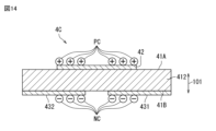
- Figures 14 and 15 are schematic cross-sectional views showing the D-D cross section of Figure 11.
- a surface charge is generated on the main surfaces of the pyroelectric element 41 (one main surface 41A and the other main surface 41B) due to the pyroelectric effect, as shown in FIG. 14.
- a positive charge PC is generated on the one main surface 41A
- a negative charge NC is generated on the other main surface 41B.
- the surface charge generated on one principal surface 41A (for example, the positive charge PC shown in FIG. 14) is not output to the outside of the infrared sensor element 4C.
- the surface charge generated on the other principal surface 41B can be output to the outside of the infrared sensor element 4C.
- a positive charge PC is generated on one principal surface 41A and a negative charge NC is generated on the other principal surface 41B as shown in FIG. 14
- no potential difference occurs between the one principal surface 41A and the other principal surface 41B. Therefore, the surface charge generated on the other principal surface 41B is not output to the outside of the infrared sensor element 4C.
- the image 8 formed in the detection area 41Aa of the one principal surface 41A moves, the surface charge generated on the other principal surface 41B is output to the outside of the infrared sensor element 4C.
- the image 8 formed in the detection area 41Aa moves from the position indicated by the symbol 8B to the position indicated by the symbol 8C, the area of the portion where the image 8 overlaps with the one-side electrode 42 decreases when viewed from the thickness direction 101 in the upper part of the paper of FIG. 11.
- the image 8 formed in the detection area 41Aa moves from the position indicated by the symbol 8B to the position indicated by the symbol 8C
- the area of the portion where the image 8 overlaps with the one-side electrode 42 increases when viewed from the thickness direction 101 in the lower part of the paper of FIG. 11.
- the second electrode 432 overlaps with the one-side electrode 42 when viewed from the thickness direction 101.
- the first electrode 431 overlaps with the one-side electrode 42 when viewed in the thickness direction 101.
- the increase or decrease in area due to the movement of the image 8 generates different charges in the increased area and decreased area.
- a negative charge NC is generated on one main surface 41A and a positive charge PC is generated on the other main surface 41B.
- a positive charge PC is generated on one main surface 41A and a negative charge NC is generated on the other main surface 41B.
- the negative charge NC generated in the increased area is output as an electrical signal from the first electrode 431 to the outside of the infrared sensor element 4C (control unit 3) via the paste 921.
- the positive charge PC generated in the decreased area is output as an electrical signal from the second electrode 432 to the outside of the infrared sensor element 4C (control unit 3) via the paste 922.
- the surface charge generated on the other main surface 41B is output to the outside, while the surface charge generated on the one main surface 41A is not output to the outside.
- it differs from the infrared sensor element 4, in which the surface charge generated on the one main surface 41A and the surface charge generated on the other main surface 41B are output to the outside.
- the electrical signal based on the charge generated on the one main surface 41A side and the electrical signal based on the charge generated on the other main surface 41B side are both extracted from the non-detection areas 41Bb, 41Bc of the other main surface 41B.
- the support section 91 only needs to support the infrared sensor element 4C from the other main surface 41B side, and does not need to support the infrared sensor element 4C from the one main surface 41A side.
- FIG. 16 is a schematic cross-sectional view corresponding to the CC cross section of FIG. 11, showing a modified example of the infrared sensor element and the support.
- a space equivalent to the thickness of the pastes 921 and 922 can be formed between the support 91 and the pyroelectric element 41.
- the support 91 does not have a step, so it is easy to use a substrate made of glass epoxy or the like as the support 91.
- the length in the thickness direction 101 (in other words, the height) can be made shorter than in the configuration shown in FIG. 6.
- an inexpensive support 91 without a step can be used.
- Second Embodiment 17 is a schematic diagram showing irradiation of infrared rays from a detection target object to two infrared sensors.
- the position detection system according to the second embodiment differs from the position detection system 1 according to the first embodiment in that the second embodiment includes two infrared sensors 21 and 22. Differences from the first embodiment will be described below. Points in common with the position detection system 1 according to the first embodiment are given the same reference numerals, and descriptions thereof will be omitted in principle, and will be described only when necessary.
- the infrared sensor 2 of the position detection system includes two infrared sensors 21 and 22.
- the position detection system also includes lenses 61 and 62 corresponding to the infrared sensors 21 and 22, respectively.
- Each of the two infrared sensors 21 and 22 has the same configuration as the infrared sensor 2 of the position detection system 1 according to the first embodiment.
- the infrared sensor element 4 of the infrared sensor 21 and the infrared sensor element 4 of the infrared sensor 22 are arranged side by side in the X-axis direction 103.
- the lens 61 is arranged facing the infrared sensor element 4 of the infrared sensor 21 in the optical axis direction 102.
- the lens 62 is arranged facing the infrared sensor element 4 of the infrared sensor 22 in the optical axis direction 102.
- the lenses 61 and 62 are arranged side by side in the X-axis direction 103.
- One main surface 41A of the pyroelectric element 41 of the infrared sensor 21 and one main surface 41A of the pyroelectric element 41 of the infrared sensor 22 are located on the same imaginary plane.
- One main surface 41A of the pyroelectric element 41 of the infrared sensor 21 and one main surface 41A of the pyroelectric element 41 of the infrared sensor 22 are examples of opposing surfaces.
- the control unit 3 (see Figure 1) is electrically connected to each of the two infrared sensors 21 and 22.
- the control unit 3 calculates the image center position k1 in the infrared sensor 21 based on the electrical signal output from the infrared sensor 21 to the control unit 3.
- the control unit 3 calculates the image center position k2 in the infrared sensor 22 based on the electrical signal output from the infrared sensor 22 to the control unit 3.
- the control unit 3 calculates the difference between the two calculated image center positions k1 and k2 .
- the control unit 3 calculates the distance L along the optical axis direction 102 between the centers C1, C2 of the lenses 61, 62 and the detection object 7 by the following equation (8).
- kd is the difference between image center positions k1 and k2 .
- D1 is the distance along the optical axis direction 102 between the centers C1 and C2 of the lenses 61 and 62 and the pyroelectric element 41.
- D2 is the distance along the X-axis direction 103 between the optical axis 61A of the lens 61 and the optical axis 62A of the lens 62.
- D2 is the distance along the X-axis direction 103 between the axis AX of the parabola constituting the curved outer edge portion of the infrared sensor 21 and the axis AX of the parabola constituting the curved outer edge portion of the infrared sensor 22.
- the control unit 3 calculates the distance L based on kd , D1 , and D2 .
- the distance between the infrared sensor 2 and the object to be detected 7 can be calculated.
- the infrared sensor element, infrared sensor, and position detection system described above can also be expressed as follows:
- An infrared sensor element having one main surface facing one side in a thickness direction and another main surface overlapping the one main surface when viewed from the thickness direction and facing the other side in the thickness direction; A first electrode provided on the first principal surface; a second-side electrode provided on the second principal surface and overlapping the first-side electrode when viewed in the thickness direction, When viewed from the thickness direction, the one electrode or the other electrode has a curved outer edge portion that is parabolic.
- Each of the one principal surface and the other principal surface may have a detection region and a non-detection region, When viewed from the thickness direction, the detection region of the one principal surface and the detection region of the other principal surface may overlap with each other,
- the one-side electrode may be provided across a detection region of the one principal surface and a non-detection region of the one principal surface, and may have the curved outer edge portion provided in the detection region of the one principal surface,
- the other-side electrode may be provided across a detection region of the other principal surface and a non-detection region of the other principal surface, When viewed from the thickness direction, a portion of the one-side electrode provided in the detection region on the one principal surface may overlap a portion of the other-side electrode provided in the detection region on the other principal surface.
- a non-detection region of the one principal surface on which the one-side electrode is provided may be located outside a non-detection region of the other principal surface on which the other-side electrode is provided.
- the other principal surface may have a detection region, a first non-detection region, and a second non-detection region
- the one electrode may have the curved outer edge
- the curved outer edge portion of the one electrode is A first curved outer edge portion overlapping the detection area of the other main surface as viewed in the thickness direction; a second curved outer edge portion that overlaps with the detection area of the other principal surface when viewed from the thickness direction and is parallel to the first curved outer edge portion
- the other electrode is a first electrode that is provided across a part of the detection region of the other principal surface and a first non-detection region of the other principal surface and overlaps a portion of the one-side electrode that has the first curved outer edge portion when viewed in the thickness direction;
- the second electrode may be electrically insulated from the first electrode, arranged across a portion of the detection area of the other main surface and a second non-detection area of the other main surface, and overlapping a portion of
- An infrared sensor according to an aspect of the present disclosure, An infrared sensor element according to any one of (1) to (4); A drive unit that moves the pyroelectric element; A control unit that controls the drive unit.
- the control unit may drive the drive unit with a sine wave.
- a position detection system (6) An infrared sensor; a lens provided opposite either the one principal surface or the other principal surface in an optical axis direction parallel to the thickness direction, the lens is provided such that an image formed by infrared rays emitted from a detection object on an opposing surface of the one principal surface and the other principal surface that faces the lens through the lens is formed from one end of the opposing surface to the other end in a Y-axis direction that is parallel to the opposing surface and parallel to the axis of a parabola that constitutes the curved outer edge portion, and is formed shorter than the opposing surface in an X-axis direction that is parallel to the opposing surface and perpendicular to the Y-axis direction,
- the control unit is The driving unit is sinusoidally driven to move the pyroelectric element along the X-axis direction; Based on the electrical signal output from at least one of the one-side electrode and the other-side electrode due to the movement of the pyroelectric element, the image center
- the control unit is The image center position may be calculated for each of the two infrared sensors;
- the distance along the optical axis direction between the center of the lens and the object to be detected may be calculated based on the difference between the two calculated image center positions, the distance along the optical axis direction between the center of the lens and the pyroelectric element, and the distance along the X-axis direction between the axis of the parabola constituting the curved outer edge portion of one of the two infrared sensors and the axis of the parabola constituting the curved outer edge portion of the other of the two infrared sensors.
Landscapes
- Physics & Mathematics (AREA)
- General Physics & Mathematics (AREA)
- Spectroscopy & Molecular Physics (AREA)
- Life Sciences & Earth Sciences (AREA)
- General Life Sciences & Earth Sciences (AREA)
- Geophysics (AREA)
- Photometry And Measurement Of Optical Pulse Characteristics (AREA)
- Geophysics And Detection Of Objects (AREA)
Abstract
L'invention concerne un élément de capteur infrarouge pouvant détecter la direction dans laquelle se trouve un objet à détecter tout en gardant une taille réduite. Cet élément de capteur infrarouge comprend : un élément pyroélectrique avec une surface principale orientée d'un côté par rapport au sens de l'épaisseur et une autre surface principale qui chevauche la première surface principale lorsque vue dans le sens de l'épaisseur et orientée de l'autre côté par rapport au sens de l'épaisseur ; une électrode sur un premier côté, placée sur l'une des surfaces principales ; et une électrode sur l'autre côté de l'autre surface principale, l'électrode sur l'autre côté chevauchant l'électrode sur le premier côté, lorsque vue dans le sens de l'épaisseur. Vue dans le sens de l'épaisseur, l'électrode du premier côté ou l'électrode de l'autre côté présente une partie de bord externe incurvée ayant une forme parabolique.
Priority Applications (2)
| Application Number | Priority Date | Filing Date | Title |
|---|---|---|---|
| CN202480041789.7A CN121368710A (zh) | 2023-08-01 | 2024-06-03 | 红外线传感器元件、红外线传感器以及位置探测系统 |
| US19/424,702 US20260110577A1 (en) | 2023-08-01 | 2025-12-18 | Infrared sensor element, infrared sensor, and position detection system |
Applications Claiming Priority (2)
| Application Number | Priority Date | Filing Date | Title |
|---|---|---|---|
| JP2023-125630 | 2023-08-01 | ||
| JP2023125630 | 2023-08-01 |
Related Child Applications (1)
| Application Number | Title | Priority Date | Filing Date |
|---|---|---|---|
| US19/424,702 Continuation US20260110577A1 (en) | 2023-08-01 | 2025-12-18 | Infrared sensor element, infrared sensor, and position detection system |
Publications (1)
| Publication Number | Publication Date |
|---|---|
| WO2025028005A1 true WO2025028005A1 (fr) | 2025-02-06 |
Family
ID=94394360
Family Applications (1)
| Application Number | Title | Priority Date | Filing Date |
|---|---|---|---|
| PCT/JP2024/020176 Pending WO2025028005A1 (fr) | 2023-08-01 | 2024-06-03 | Élément de capteur infrarouge, capteur infrarouge et système de détection de position |
Country Status (3)
| Country | Link |
|---|---|
| US (1) | US20260110577A1 (fr) |
| CN (1) | CN121368710A (fr) |
| WO (1) | WO2025028005A1 (fr) |
Citations (4)
| Publication number | Priority date | Publication date | Assignee | Title |
|---|---|---|---|---|
| JPS5912075U (ja) * | 1982-07-14 | 1984-01-25 | 株式会社堀場製作所 | 移動物検知用赤外線検出器 |
| WO1999041575A1 (fr) * | 1998-02-13 | 1999-08-19 | Matsushita Electric Industrial Co., Ltd. | Element detecteur a infrarouge, et unite capteur a infrarouge et detecteur a infrarouge utilisant ledit element detecteur |
| JPH11281490A (ja) * | 1998-03-30 | 1999-10-15 | Shimadzu Corp | 焦電型放射温度検出器 |
| JP2013092411A (ja) * | 2011-10-25 | 2013-05-16 | Murata Mfg Co Ltd | 赤外線検知装置 |
-
2024
- 2024-06-03 CN CN202480041789.7A patent/CN121368710A/zh active Pending
- 2024-06-03 WO PCT/JP2024/020176 patent/WO2025028005A1/fr active Pending
-
2025
- 2025-12-18 US US19/424,702 patent/US20260110577A1/en active Pending
Patent Citations (4)
| Publication number | Priority date | Publication date | Assignee | Title |
|---|---|---|---|---|
| JPS5912075U (ja) * | 1982-07-14 | 1984-01-25 | 株式会社堀場製作所 | 移動物検知用赤外線検出器 |
| WO1999041575A1 (fr) * | 1998-02-13 | 1999-08-19 | Matsushita Electric Industrial Co., Ltd. | Element detecteur a infrarouge, et unite capteur a infrarouge et detecteur a infrarouge utilisant ledit element detecteur |
| JPH11281490A (ja) * | 1998-03-30 | 1999-10-15 | Shimadzu Corp | 焦電型放射温度検出器 |
| JP2013092411A (ja) * | 2011-10-25 | 2013-05-16 | Murata Mfg Co Ltd | 赤外線検知装置 |
Also Published As
| Publication number | Publication date |
|---|---|
| US20260110577A1 (en) | 2026-04-23 |
| CN121368710A (zh) | 2026-01-20 |
Similar Documents
| Publication | Publication Date | Title |
|---|---|---|
| US6049080A (en) | Pyroelectric infrared sensor device | |
| JP5809753B2 (ja) | 光学式測距装置および電子機器 | |
| WO1988004038A1 (fr) | Detecteur de mouvement | |
| EP2257849B1 (fr) | Retour de peigne capacitif pour un miroir de balayage à haute vitesse | |
| WO2013111366A1 (fr) | Capteur à infrarouge de type pyroélectrique | |
| WO2025028005A1 (fr) | Élément de capteur infrarouge, capteur infrarouge et système de détection de position | |
| US20170357075A1 (en) | Optical element | |
| KR20230138035A (ko) | 작동 디바이스 | |
| JP2001166874A (ja) | 入力装置 | |
| CN109983308A (zh) | 位移检测装置和设置有它的镜筒以及成像装置 | |
| KR102645131B1 (ko) | 액체 렌즈를 포함하는 카메라 모듈 및 그의 제어 방법 | |
| JP5531062B2 (ja) | マスクの構造 | |
| JP2018084455A (ja) | 変位検出装置およびこれを備えたレンズ鏡筒、撮像装置 | |
| WO2006095274A1 (fr) | Paire de cameras utilisant de lentilles a base de fluide | |
| KR102645839B1 (ko) | 액체 렌즈를 포함하는 카메라 모듈 | |
| JP2012027336A (ja) | センサ装置 | |
| US20230221544A1 (en) | Mems-mirror device, lidar device and vehicle comprising a lidar device | |
| JP2015114474A (ja) | 光学装置 | |
| KR102648388B1 (ko) | 조리개 및 이를 포함하는 렌즈 어셈블리 | |
| JP5233236B2 (ja) | 光走査装置 | |
| JP2014006078A (ja) | 走査型赤外線センサ | |
| JP2013019857A (ja) | 焦電型センサ素子 | |
| JPH09243452A (ja) | 赤外線センサ | |
| BR102023017171A2 (pt) | Elemento de dobramento do caminho da luz, módulo de câmera e dispositivo eletrônico | |
| CN118426162A (zh) | 波长可变干涉滤波器 |
Legal Events
| Date | Code | Title | Description |
|---|---|---|---|
| 121 | Ep: the epo has been informed by wipo that ep was designated in this application |
Ref document number: 24848666 Country of ref document: EP Kind code of ref document: A1 |
|
| NENP | Non-entry into the national phase |
Ref country code: DE |