WO2025057770A1 - PROCÉDÉ DE TRAITEMENT DE SUBSTRAT DE SiC, PROCÉDÉ D'ÉLIMINATION DE COUCHE AFFECTÉE PAR LE TRAITEMENT DE SUBSTRAT DE SiC, ET PROCÉDÉ DE RÉDUCTION DE RUGOSITÉ DE SURFACE DE SUBSTRAT DE SiC - Google Patents
PROCÉDÉ DE TRAITEMENT DE SUBSTRAT DE SiC, PROCÉDÉ D'ÉLIMINATION DE COUCHE AFFECTÉE PAR LE TRAITEMENT DE SUBSTRAT DE SiC, ET PROCÉDÉ DE RÉDUCTION DE RUGOSITÉ DE SURFACE DE SUBSTRAT DE SiC Download PDFInfo
- Publication number
- WO2025057770A1 WO2025057770A1 PCT/JP2024/031151 JP2024031151W WO2025057770A1 WO 2025057770 A1 WO2025057770 A1 WO 2025057770A1 JP 2024031151 W JP2024031151 W JP 2024031151W WO 2025057770 A1 WO2025057770 A1 WO 2025057770A1
- Authority
- WO
- WIPO (PCT)
- Prior art keywords
- sic substrate
- crucible
- sic
- etching
- processing
- Prior art date
- Legal status (The legal status is an assumption and is not a legal conclusion. Google has not performed a legal analysis and makes no representation as to the accuracy of the status listed.)
- Pending
Links
Images


Classifications
-
- C—CHEMISTRY; METALLURGY
- C30—CRYSTAL GROWTH
- C30B—SINGLE-CRYSTAL GROWTH; UNIDIRECTIONAL SOLIDIFICATION OF EUTECTIC MATERIAL OR UNIDIRECTIONAL DEMIXING OF EUTECTOID MATERIAL; REFINING BY ZONE-MELTING OF MATERIAL; PRODUCTION OF A HOMOGENEOUS POLYCRYSTALLINE MATERIAL WITH DEFINED STRUCTURE; SINGLE CRYSTALS OR HOMOGENEOUS POLYCRYSTALLINE MATERIAL WITH DEFINED STRUCTURE; AFTER-TREATMENT OF SINGLE CRYSTALS OR A HOMOGENEOUS POLYCRYSTALLINE MATERIAL WITH DEFINED STRUCTURE; APPARATUS THEREFOR
- C30B23/00—Single-crystal growth by condensing evaporated or sublimed materials
- C30B23/02—Epitaxial-layer growth
-
- C—CHEMISTRY; METALLURGY
- C30—CRYSTAL GROWTH
- C30B—SINGLE-CRYSTAL GROWTH; UNIDIRECTIONAL SOLIDIFICATION OF EUTECTIC MATERIAL OR UNIDIRECTIONAL DEMIXING OF EUTECTOID MATERIAL; REFINING BY ZONE-MELTING OF MATERIAL; PRODUCTION OF A HOMOGENEOUS POLYCRYSTALLINE MATERIAL WITH DEFINED STRUCTURE; SINGLE CRYSTALS OR HOMOGENEOUS POLYCRYSTALLINE MATERIAL WITH DEFINED STRUCTURE; AFTER-TREATMENT OF SINGLE CRYSTALS OR A HOMOGENEOUS POLYCRYSTALLINE MATERIAL WITH DEFINED STRUCTURE; APPARATUS THEREFOR
- C30B29/00—Single crystals or homogeneous polycrystalline material with defined structure characterised by the material or by their shape
- C30B29/10—Inorganic compounds or compositions
- C30B29/36—Carbides
-
- C—CHEMISTRY; METALLURGY
- C30—CRYSTAL GROWTH
- C30B—SINGLE-CRYSTAL GROWTH; UNIDIRECTIONAL SOLIDIFICATION OF EUTECTIC MATERIAL OR UNIDIRECTIONAL DEMIXING OF EUTECTOID MATERIAL; REFINING BY ZONE-MELTING OF MATERIAL; PRODUCTION OF A HOMOGENEOUS POLYCRYSTALLINE MATERIAL WITH DEFINED STRUCTURE; SINGLE CRYSTALS OR HOMOGENEOUS POLYCRYSTALLINE MATERIAL WITH DEFINED STRUCTURE; AFTER-TREATMENT OF SINGLE CRYSTALS OR A HOMOGENEOUS POLYCRYSTALLINE MATERIAL WITH DEFINED STRUCTURE; APPARATUS THEREFOR
- C30B33/00—After-treatment of single crystals or homogeneous polycrystalline material with defined structure
- C30B33/08—Etching
- C30B33/12—Etching in gas atmosphere or plasma
Definitions
- the present invention relates to a method for processing a SiC substrate.
- SiC substrate as-sliced substrate
- Conventional SiC substrate processing involves steps such as lapping and/or grinding and polishing, which gradually reduce the surface roughness.
- Patent Document 1 describes a method for reducing macro-step bunching on the substrate surface by heating and etching a SiC substrate in an environment with the vapor pressure of a gas phase species containing Si element and a gas phase species containing C element.
- Patent Document 2 describes a method for reducing the process-affected layer of a substrate by heating and etching a SiC substrate in an environment with the vapor pressure of a gas phase species containing Si element and a gas phase species containing C element.
- the inventors have discovered the following problem. That is, it is the initial stages of processing that cause the formation and expansion of a process-induced layer on the SiC substrate, making it difficult to remove this process-induced layer in the middle and final stages of processing. In addition, significant loss of raw materials occurs in the initial stages of processing, which is a factor that reduces the sustainability of SiC semiconductor device manufacturing.
- the present invention therefore aims to provide a new method for processing SiC substrates. More specifically, it aims to provide a non-contact processing method that can replace the initial stage of conventional SiC substrate processing. Furthermore, it aims to provide a processing method that can reduce the loss of raw materials that occurs in this initial stage of processing.
- One embodiment of the present invention for achieving the above object is a method for processing a SiC substrate, which is the following method [1] to [46].
- Method [1] is a method for processing a SiC substrate, which includes an annealing step in which the SiC substrate is heated inside a crucible made of SiC, and in the annealing step, the inside of the crucible is maintained in an inert gas environment.
- method [1] by strongly promoting both the sublimation reaction and the recrystallization reaction on the surface of the SiC substrate, atoms are vigorously exchanged between the surface layer of the SiC substrate and the environment, that is, the metabolism of the atoms that make up the surface layer of the SiC substrate can be strongly promoted. This makes it possible to remove the process-induced alteration layer contained in the surface layer in a short period of time.
- the surface layer of the SiC substrate is leveled in the metabolism process, resulting in a SiC substrate with low surface roughness.
- Method [2] is a method for treating a SiC substrate according to method [1], in which the annealing step includes etching one surface of the SiC substrate and simultaneously growing the other surface of the SiC substrate.
- Method [3] is a method for processing a SiC substrate according to method [2], in which the annealing step includes making the amount of etching on one surface approximately equal to the amount of growth on the other surface, thereby making the thickness of the SiC substrate approximately equal before and after the annealing step.
- Method [4] is a method for treating a SiC substrate according to method [2], which includes increasing the thickness of the SiC substrate before and after the annealing step by reducing the amount of etching on one surface relative to the amount of growth on the other surface.
- Method [5] is any one of methods [1] to [4], in which the crucible comprises a base having an opening and a lid, and the interior of the crucible is formed by covering the opening of the base with the lid.
- Method [6] is any one of methods [1] to [5], in which the SiC substrate is supported by a substrate support during the annealing step.
- Method [7] is a method for processing a SiC substrate according to method [6], in which the substrate support is formed integrally with the crucible.
- Method [8] is a method for processing a SiC substrate, which is method [6] or [7], in which the substrate support is made of SiC.
- Method [9] is any one of methods [6] to [8], in which the SiC substrate is supported from below the C-face by a substrate support with the Si-face facing up and the C-face facing down.
- Method [10] is any one of methods [6] to [9], in which, in the annealing step, the SiC substrate is supported in the hollow inside of the crucible by a substrate support.
- Method [11] is any one of methods [6] to [10], in which, in the annealing step, the SiC substrate is placed inside the crucible so that one surface of the SiC substrate faces directly against the inner wall of the crucible, and the other surface of the SiC substrate faces directly against the inner wall of the crucible.
- Method [12] is any one of methods [6] to [11], in which the SiC substrate is disposed approximately at the center inside the crucible.
- Method [13] is any one of methods [1] to [12] for treating a SiC substrate, in which the pressure inside the crucible during the annealing step is 1 kPa or more.
- Method [14] is any one of methods [1] to [12] for treating a SiC substrate, in which the pressure inside the crucible during the annealing step is 5 kPa or more.
- Method [15] is any one of methods [1] to [12] for treating a SiC substrate, in which the pressure inside the crucible during the annealing step is 10 kPa or more.
- Method [16] is any one of methods [1] to [15], in which the temperature inside the crucible during the annealing step is 1800°C or higher, for treating a SiC substrate.
- Method [17] is any one of methods [1] to [15], in which the temperature inside the crucible during the annealing step is 2000°C or higher, for treating a SiC substrate.
- Method [18] is any one of methods [1] to [15], in which the temperature inside the crucible during the annealing step is 2200°C or higher, for treating a SiC substrate.
- Method [19] is a method for treating a SiC substrate which is any one of methods [1] to [18], in which the combination of pressure and temperature inside the crucible during the annealing step is 1 kPa or more and 1800°C or more.
- Method [20] is a method for treating a SiC substrate which is any one of methods [1] to [18], in which the combination of pressure and temperature inside the crucible during the annealing step is 5 kPa or more and 2000°C or more.
- Method [21] is a method for treating a SiC substrate which is any one of methods [1] to [18], in which the combination of pressure and temperature inside the crucible during the annealing step is 5 kPa or more and 2200°C or more.
- Method [22] is a method for treating a SiC substrate which is any one of methods [1] to [18], in which the combination of pressure and temperature inside the crucible during the annealing step is 10 kPa or more and 2200°C or more.
- Method [23] is any one of methods [1] to [22], in which a temperature gradient is formed inside the crucible in the direction penetrating the SiC substrate during the annealing step.
- Method [24] is a method for treating a SiC substrate according to method [23], in which the temperature gradient is formed such that the temperature decreases from the C-face side of the SiC substrate toward the Si-face side.
- Method [25] is any one of methods [1] to [24], in which the inert gas environment in the annealing step contains Ar gas as the inert gas, for treating a SiC substrate.
- Method [26] is any one of methods [1] to [25], in which no protective film is formed on the surface of the SiC substrate during the annealing process.
- Method [27] is any one of methods [1] to [26], in which the crucible is made of polycrystalline SiC, for treating a SiC substrate.
- Method [28] is any one of methods [1] to [27], in which the annealing step includes a step of accommodating the SiC substrate inside a crucible, the crucible including a base having an opening and a lid, and the accommodating step includes placing the SiC substrate through the opening of the base and placing the lid on the base to cover the opening of the base, thereby accommodating the SiC substrate inside the crucible.
- Method [29] is any one of methods [1] to [28], in which the annealing step includes a housing step of housing the SiC substrate inside a crucible, and the housing step includes supporting the SiC substrate in the hollow inside the crucible with a substrate support.
- Method [30] is any one of methods [1] to [29], in which the annealing step includes a step of housing the SiC substrate inside a crucible, and the housing step includes directly opposing one surface of the SiC substrate to an inner wall of the crucible and directly opposing the other surface of the SiC substrate to the inner wall of the crucible.
- Method [32] is any one of methods [1] to [31], in which the annealing step includes a heating step of heating a crucible, and the heating step includes heating the crucible and generating a gas composed of one or both of Si and C elements from the crucible to the inside of the crucible.
- Method [34] is any one of methods [1] to [32], in which the annealing step includes a heating step of heating the crucible, and the heating step includes introducing an inert gas into the crucible and maintaining the pressure inside the crucible at 5 kPa or more.
- Method [35] is a method for treating a SiC substrate which is any one of methods [1] to [32], in which the annealing step includes a heating step of heating the crucible, and the heating step includes introducing an inert gas into the crucible and maintaining the pressure inside the crucible at 10 kPa or more.
- Method [36] is any one of methods [1] to [35], wherein the annealing step comprises a heating step of heating the crucible;
- the heating step is a method for treating a SiC substrate, which includes heating the crucible and maintaining the temperature inside the crucible at 1800° C. or higher.
- Method [37] is any one of methods [1] to [35], wherein the annealing step comprises a heating step of heating the crucible;
- the heating step is a method for treating a SiC substrate, which includes heating the crucible and maintaining the temperature inside the crucible at 2000° C. or higher.
- Method [38] is any one of methods [1] to [35], wherein the annealing step comprises a heating step of heating the crucible;
- the heating step is a method for treating a SiC substrate, which includes heating the crucible and maintaining the temperature inside the crucible at 2200° C. or higher.
- Method [39] is a method for treating a SiC substrate which is any one of methods [1] to [38], in which the annealing step includes a heating step of heating a crucible, and the heating step includes introducing an inert gas into the crucible and maintaining the pressure inside the crucible at 1 kPa or more, and heating the crucible and maintaining the temperature inside the crucible at 1800°C or more.
- Method [41] is any one of methods [1] to [38], in which the annealing step includes a heating step of heating a crucible, and the heating step includes introducing an inert gas into the crucible and maintaining the pressure inside the crucible at 5 kPa or more, and heating the crucible and maintaining the temperature inside the crucible at 2200°C or more.
- Method [42] is a method for treating a SiC substrate which is any one of methods [1] to [38], in which the annealing step includes a heating step of heating a crucible, and the heating step includes introducing an inert gas into the crucible and maintaining the pressure inside the crucible at 10 kPa or more, and heating the crucible and maintaining the temperature inside the crucible at 2200°C or more.
- Method [43] is any one of methods [1] to [42], in which the annealing step includes a heating step of heating the crucible, and the heating step includes forming a temperature gradient inside the crucible in a direction penetrating the SiC substrate.
- Method [45] is any one of methods [1] to [44], in which the annealing step includes a heating step of heating a crucible, the crucible including a base having an opening and a lid, and the heating step includes creating a temperature difference between the base and the lid.
- Method [46] is any one of methods [1] to [45], which is a method for processing a SiC substrate, and does not include a step of performing a mechanical treatment on the SiC substrate after the annealing step.
- one embodiment of the present invention for achieving the above object is a method for removing a process-induced alteration layer from a SiC substrate, which is the following method [47] to [49].
- Method [47] is a method for removing a process-damaged layer from a SiC substrate, which includes performing any one of methods [1] to [46] on a SiC substrate having a process-damaged layer, thereby removing the process-damaged layer.
- Method [48] is a method for removing a process-damaged layer from a SiC substrate, which is method [47] and includes carrying out any one of methods [1] to [46] on a SiC substrate on which a process-damaged layer has been formed by mechanical processing.
- Method [49] is a method for removing a process-damaged layer of a SiC substrate according to method [47] or [48], in which the annealing step includes exchanging atoms between the surface layer of the SiC substrate and an inert gas environment to remove the process-damaged layer.
- one embodiment of the present invention for achieving the above object is a method for reducing the surface roughness of a SiC substrate, which is the following method [50] to [52].
- Method [50] is a method for reducing the surface roughness of a SiC substrate, which involves carrying out any one of methods [1] to [46] on a SiC substrate having an arithmetic mean roughness Ra of the Si surface of 15 nm or more, thereby reducing the arithmetic mean roughness Ra.
- Method [51] is a method for reducing the surface roughness of a SiC substrate, which is the same as method [50], and includes performing any one of methods [1] to [46] on a SiC substrate that has been subjected to mechanical processing.
- Method [52] is a method for reducing the surface roughness of a SiC substrate according to method [50] or [51], in which the annealing step includes exchanging atoms between the surface of the SiC substrate and an inert gas environment to smooth the surface.
- the present invention can provide a new processing method for SiC substrates. More specifically, it can provide a non-contact processing method that can replace the initial stage of conventional SiC substrate processing. Furthermore, it can provide a processing method that can reduce the loss of raw materials that occurs in this initial processing stage.
- FIG. 2 is a diagram illustrating the concept of a processing method according to an embodiment of the present invention.
- FIG. 2 is a diagram illustrating the concept of a processing method according to an embodiment of the present invention.
- FIG. 2 is a diagram illustrating the concept of a processing method according to an embodiment of the present invention.
- FIG. 2 is a diagram illustrating the concept of a processing method according to an embodiment of the present invention.
- FIG. 2 is a diagram illustrating the concept of a processing method according to an embodiment of the present invention.
- FIG. 1 is an explanatory diagram of a first preferred embodiment of the present invention.
- FIG. 13 is an explanatory diagram of a modified example of the first preferred embodiment of the present invention.
- FIG. 1 is an explanatory diagram of a first preferred embodiment of the present invention.
- FIG. 1 is an explanatory diagram of a first preferred embodiment of the present invention.
- FIG. 2 is an illustration of a second preferred embodiment of the present invention.
- FIG. 2 is an illustration of a second preferred embodiment of the present invention.
- FIG. 13 is an illustration of a third preferred embodiment of the present invention.
- FIG. 13 is an explanatory diagram of a fourth preferred embodiment of the present invention.
- FIG. 13 is an explanatory diagram of a fifth preferred embodiment of the present invention.
- FIG. 1 is an explanatory diagram of the results of an embodiment of the present invention.
- FIG. 1 is an explanatory diagram of the results of an embodiment of the present invention.
- FIG. 1 is an explanatory diagram of the results of an embodiment of the present invention.
- FIG. 1 is an explanatory diagram of the results of an embodiment of the present invention.
- One embodiment of the present invention is a method for processing a SiC substrate.
- This processing method includes an annealing step in which the SiC substrate is heated inside a crucible made of SiC.
- the inside of the crucible is maintained in an inert gas environment.
- inert gas environment refers to an environment containing an inert gas.
- inert gas include Ar gas and N2 gas.
- the inert gas environment of the present processing method contains Ar gas as an inert gas.
- Ar gas it is preferable that the majority of the inert gas is Ar gas, and it is also preferable that the inert gas is substantially entirely Ar gas.
- a part of the inert gas may be N2 gas. That is, the annealing step of the present processing method can be said to be a step of annealing a SiC substrate in an inert gas environment.
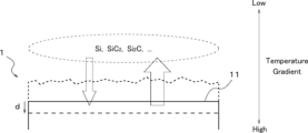
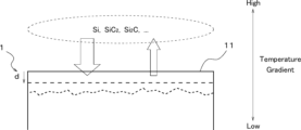
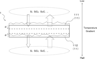
- Figs. 1 to 5 show a SiC substrate 1, a surface 11 (Si face 111 and C face 112) of the SiC substrate, a processing-affected layer 12 of the SiC substrate, a crucible 2 made of SiC, and a base 21 and a lid 22 of the crucible 2.
- processing-affected layer refers to a layer that includes damage caused by mechanical processing and is likely to adversely affect the performance of a SiC semiconductor device.
- An example of a processing-affected layer is a surface layer that has undergone mechanical processing on the side of the Si face 111 on which a device will be formed in the future.
- mechanical processing refers to a process that physically destroys the atomic arrangement of the substrate.
- mechanical processing include ingot cutting (e.g., multi-wire saw cutting, laser cutting, discharge cutting), grinding, and polishing (e.g., mechanical polishing, chemical mechanical polishing).
- Heating the SiC substrate 1 causes, for example, the reactions shown in Chemical Formulas 1 to 3. That is, heating the SiC substrate 1 causes the source gas to sublimate from the SiC substrate 1 and recrystallize on the SiC substrate 1.
- source gas refers to a gas composed of one or both of the Si element and the C element. Examples of source gas include Si gas, SiC2 gas, Si2C gas, and a mixture of these gases.
- the reaction of Chemical Formula 1 corresponds to a thermal decomposition reaction.
- Si gas is desorbed from the SiC substrate 1, and C remains in the SiC substrate 1.
- the thermal decomposition reaction is dominant, the SiC substrate 1 is carbonized.
- the reaction of Chemical formula 2 corresponds to a sublimation reaction.
- C in the SiC substrate 1 sublimes as a raw material gas.
- the SiC substrate 1 is etched.
- the reaction of Chemical formula 3 corresponds to a recrystallization reaction.
- the raw material gas recrystallizes into the SiC substrate 1.
- the recrystallization reaction is dominant, the SiC substrate 1 grows.
- This processing method is based on the idea of strongly promoting both the sublimation reaction and the recrystallization reaction, thereby vigorously exchanging atoms between the surface layer of the SiC substrate 1 and the annealing environment, i.e. strongly promoting the metabolism of the atoms that make up the surface layer of the SiC substrate 1.
- surface layer refers to the layer ranging from the surface to a specified depth.
- this processing method involves inducing the metabolism of atoms constituting the surface layer ranging from the surface 11 to a depth d.
- the depth d depends on the intensity of the sublimation and recrystallization reactions. This makes it possible to remove the process-affected layer 12 included in the range from the surface 11 to the depth d in a short period of time.
- the surface layer of the SiC substrate 1 is leveled in the metabolism process, thereby realizing a SiC substrate 1 with low surface roughness.
- this processing method can be used both as a method for removing the process-affected layer 12 of the SiC substrate 1 and as a method for reducing the roughness of the surface 11 of the SiC substrate 1.
- the atoms that make up the surface layer of the SiC substrate 1 are macroscopically reduced, and the surface 11 is etched.
- the balance between the reduction and increase of microscopic atoms is biased towards reduction, resulting in a macroscopic reduction in atoms.
- the repeated reduction of microscopic atoms results in a macroscopic reduction in atoms.
- the atoms that make up the surface layer of the SiC substrate 1 increase macroscopically, and the surface 11 grows.
- the balance between the decrease and increase of microscopic atoms is biased towards an increase, resulting in a macroscopic increase in atoms.
- a macroscopic increase in atoms occurs as a result of repeated increases in microscopic atoms.
- the etching and growth of this processing method can always remove the process-affected layer 12 contained within the range from the surface 11 to the depth d.
- the etching of this processing method can remove the process-affected layer 12 from a range wider than the etching range.
- the growth of this processing method can form a grown layer free of the effects of the process-affected layer 12 in a single process.
- conventional etching cannot remove the process-affected layer that is not contained within the etching range, and conventional growth cannot remove the process-affected layer at all.
- the process includes controlling the etching and growth of surface 11 by controlling the macroscopic flow of the source gas.
- means for controlling the macroscopic flow of the source gas include controlling a temperature gradient and controlling a source gas concentration gradient.
- This processing method induces the metabolism of atoms constituting the surface layer of the SiC substrate 1 on both the Si surface 111 and the C surface 112, that is, includes processing both the Si surface 111 and the C surface 112 simultaneously.
- FIG. 4 when a temperature gradient is formed in a direction in which the temperature decreases from the C surface 112 side to the Si surface 111 side, the macroscopic flow of the raw material gas is in a direction away from the Si surface 111 and toward the C surface 112. At this time, the Si surface 111 is etched, and at the same time, the C surface 112 grows.
- FIG. 4 shows that is, includes processing both the Si surface 111 and the C surface 112 simultaneously.
- This processing method includes simultaneously processing both the Si surface 111 and the C surface 112 while maintaining the thickness of the SiC substrate 1.
- the etching rate or growth rate on the surface 11 largely depends on the temperature gradient near the surface 11.
- the temperature gradient itself changes over time, but since the Si surface 111 and the C surface 112 are spatially very close to each other (for example, about 400 ⁇ m), the temperature gradients on the Si surface 111 and the C surface 112 are always approximately the same.
- the etching rate on one surface 11 and the growth rate on the other surface 11 are always approximately the same.
- the etching amount on one surface 11 and the growth amount on the other surface 11 are approximately the same, and the substrate thickness of the SiC substrate 1 is maintained.
- the raw material loss associated with the processing of the SiC substrate 1 can be substantially reduced to zero within the substrate.
- the processing method X includes a preparation step S1 of preparing a SiC substrate 1.
- the preparation step S1 may include preparing a plurality of SiC substrates 1.
- the preparation step S1 may include preparing a substrate having a processing-affected layer as the SiC substrate 1.
- This substrate may be a substrate (e.g., an as-sliced substrate) on which a processing-affected layer has been formed through mechanical processing (e.g., ingot cutting, grinding, mechanical polishing, chemical mechanical polishing).
- the processing method X can be used as a method for removing the processing-affected layer 12 of the SiC substrate 1.
- This SiC substrate may be a SiC substrate that has been subjected to mechanical processing (e.g., ingot cutting, grinding).
- the processing method X can be used as a method for reducing the roughness of the surface 11 of the SiC substrate 1.
- the preparation step S1 involves preparing a substrate with no protective film formed on its surface as the SiC substrate 1. This allows both the Si surface 111 and the C surface 112 to be processed simultaneously.
- the processing method X includes an annealing step S2 of heating the SiC substrate 1 inside a crucible 2.
- the inner wall of the crucible 2 is made of SiC (e.g., polycrystalline SiC, single crystal SiC). It is also preferable that substantially the entire crucible 2 is made of SiC. This SiC is preferably polycrystalline SiC.
- the crucible 2 comprises a base 21 having an opening, and a lid 22.
- the interior of the crucible 2 is formed by covering the opening of the base 21 with the lid 22.
- the SiC substrate 1 is placed inside the crucible 2 with the opening of the base 21 facing upwards and the lid 22 placed on the base 21 covering the opening of the base 21.
- the SiC substrate 1 is supported by a substrate support 3.
- the substrate support 3 is formed integrally with the base 21 or the lid 22.
- the substrate support 3 may be provided from the inner wall of the base 21, or from the inner wall of the lid 22.
- the substrate support 3 may be formed separately from the base 21 or the lid 22.
- the substrate support 3 is preferably placed on the inner bottom of the base 21.
- the substrate support 3 is preferably made of SiC (e.g., polycrystalline SiC, single crystal SiC).
- the SiC substrate 1 is supported by the substrate support 3 from below the C-face 112 with the Si-face 111 facing up and the C-face 112 facing down.
- the substrate support 3 may be supported from below the Si-face 111 with the Si-face 111 facing down and the C-face 112 facing up.
- the SiC substrate 1 is supported by the substrate support 3 via a small contact area, and as a result, is supported in the hollow inside the crucible 2.
- the SiC substrate 1 may be supported at three or more points, or may be supported by a line such as a circle.
- the SiC substrate 1 is preferably disposed inside the crucible 2 such that one surface 11 directly faces the inner wall of the crucible 2 and the other surface 11 directly faces the inner wall of the crucible 2 by being supported in the hollow inside the crucible 2.
- the term "directly facing" refers to two members facing each other without being obstructed by other members.
- the SiC substrate 1 is preferably supported in the hollow and disposed approximately in the center inside the crucible 2.
- the inside of crucible 2 is maintained in an inert gas environment.
- the pressure inside crucible 2 is 1 kPa or more (or more than 1 kPa). This pressure may be 5 kPa or more (or more than 5 kPa), 10 kPa or more (or more than 10 kPa), or 100 kPa or more (or more than 100 kPa). There is no particular upper limit to this pressure, but it is preferably 300 kPa or less (or less than 300 kPa).
- the temperature inside crucible 2 is 1800°C or more (or more than 1800°C).
- This temperature is preferably 1900°C or higher (or more than 1900°C), preferably 2000°C or higher (or more than 2000°C), preferably 2100°C or higher (or more than 2100°C), and preferably 2200°C or higher (or more than 2200°C).
- a preferred combination of pressure and temperature inside the crucible 2 is 1 kPa or higher (or more than 1 kPa) and 1800°C or higher (or more than 1800°C).
- This combination is preferably 1 kPa or higher (or more than 1 kPa) and 1900°C or higher (or more than 1900°C), and preferably 1 kPa or higher (or more than 1 kPa) and 2000°C or higher (or more than 2000°C).
- This combination is preferably a combination of 10 kPa or more (or over 10 kPa) and 1800°C or more (or over 1800°C), more preferably a combination of 10 kPa or more (or over 10 kPa) and 1900°C or more (or over 1900°C), and more preferably a combination of 10 kPa or more (or over 10 kPa) and 2000°C or more (or over 2000°C).
- a particularly preferred combination of pressure and temperature inside the crucible 2 is 5 kPa or more (or more than 5 kPa) and 2000°C or more (or more than 2000°C).
- This combination is preferably 5 kPa or more (or more than 5 kPa) and 2200°C or more (or more than 2200°C), more preferably 10 kPa or more (or more than 10 kPa) and 2000°C or more (or more than 2200°C), more preferably 10 kPa or more (or more than 10 kPa) and 2200°C or more (or more than 2200°C).
- a temperature gradient is formed inside the crucible 2.
- a temperature difference is formed between the base 21 and the lid 22.
- This temperature gradient is formed in a direction penetrating the SiC substrate 1.
- This temperature gradient is formed in a direction in which the temperature decreases from the C-face 112 side toward the Si-face 111 side. Note that this temperature gradient may also be formed in a direction in which the temperature decreases from the Si-face 111 toward the C-face 112.
- processing method X by annealing the SiC substrate 1 inside the crucible 2, it is possible to etch the Si face 111 while maintaining the substrate thickness of the SiC substrate 1, and at the same time, grow the C face 112.
- the process-affected layer 12 included in the surface layer on the Si face 111 side can be sufficiently removed, and the roughness of both the Si face 111 and the C face 112 can be reduced.
- the temperature gradient is reversed, it is possible to grow the Si face 111 while maintaining the substrate thickness of the SiC substrate 1, and at the same time, etch the C face 112.
- processing method X the SiC substrate 1 is supported inside the crucible 2 in the manner described above, so that etching or growth of the surface 11 can be performed under suitable conditions.
- the crucible 2 and the substrate support 3 are made of SiC, raw material gas is generated from the crucible 2 and the substrate support 3 inside the crucible 2, and a state in which sufficient raw material gas is present inside the crucible 2 is maintained. As a result, both the sublimation reaction and the recrystallization reaction can be strongly promoted.
- both the sublimation reaction and the recrystallization reaction are strongly promoted, so that carbonization of the crucible 2 can be suppressed.
- gas that does not recrystallize in the SiC substrate 1 can be recrystallized in the crucible 2 and the substrate support 3 and recovered, and as a result, raw material loss can be substantially reduced to zero throughout the crucible 2 and the inside of the crucible 2.
- the crucible 2 is made of polycrystalline SiC, the amount of source gas generated from a unit area of the crucible 2 is greater than the amount of source gas generated from a unit area of the SiC substrate 1, which is single crystal SiC, so the amount of etching of the Si surface 111 is slightly smaller and the amount of growth of the C surface 112 is slightly larger. As a result, the thickness of the SiC substrate 1 can be slightly increased before and after heating.
- the interior of the crucible 2 is formed by placing the lid 22 on the base 21, so that while the interior of the crucible 2 is a closed environment, gas (e.g., inert gas) can pass between the inside and outside of the crucible 2 through the small gap between the base 21 and the lid 22. In other words, the gas inside the crucible 2 can be adjusted without opening the crucible 2.
- gas e.g., inert gas
- the etching amount of the Si-face 111 and the growth amount on the C-face 112 can be approximately the same, and the substrate thickness of the SiC substrate 1 can be approximately the same before and after heating.
- the inside of the crucible 2 is maintained in an inert gas environment in the manner described above, so that etching or growth of the surface 11 can be performed under suitable conditions.
- the diffusion of the source gas sublimated from the SiC substrate 1 is suppressed, the source gas concentration in the vicinity of the SiC substrate 1 increases, and the thermal motion of the source gas becomes intense. As a result, both the sublimation reaction and the recrystallization reaction are strongly promoted on the surface 11 of the SiC substrate 1.
- the crucible 2 may be placed inside the large crucible 4.
- the inner wall of the large crucible 4 is made to contain a C element storage material.
- C element storage material refers to a material that stores C element when heated. Examples of C element storage materials include Ta and TaC. It is also preferable that substantially the entire large crucible 4 is made to contain a C element storage material.
- the inner wall of the large crucible 4 is preferably made of a Si gas generating material.
- Si gas generating material refers to a material that generates Si gas when heated. Examples of Si gas generating materials include Si and tantalum silicide. Substantially the entire large crucible 4 may be made of a Si gas generating material.
- a Si gas source may be disposed inside the large crucible 4 and outside the crucible 2.
- the term "Si gas source” refers to a member that generates Si gas when heated.
- An example of a Si gas source is Si (e.g., Si chips).
- the large crucible 4 comprises a large base 41 with an opening, and a large lid 42.
- the interior of the large crucible 4 is formed by covering the opening of the large base 41 with the large lid 42.
- the crucible 2 is placed inside the large crucible 4 with the opening of the large base 41 facing upwards and the large lid 42 placed on the large base 41 covering the opening of the large base 41.
- processing method X by disposing crucible 2 inside large crucible 4 in the manner described above, etching or growth of surface 11 can be performed under suitable conditions.
- the inner wall of the large crucible 4 is made of a material that occludes the C element, so that the C element is removed from the raw material gas generated from the crucible 2, and the outside of the crucible 2 becomes an environment dominated by the Si element. As a result, carbonization of the crucible 2 can be suppressed.
- the inner wall of the large crucible 4 is made of a material that generates Si gas, or a Si gas source is disposed inside the large crucible 4 and outside the crucible 2, so that the outside of the crucible 2 is an environment dominated by Si elements. As a result, carbonization of the crucible 2 can be suppressed.
- the steps included in the annealing step S2 will be described in detail below.
- Storage step S21> The annealing step S2 includes a housing step S21 of housing the SiC substrate 1 inside the crucible 2.
- the accommodation step S21 includes placing the SiC substrate 1 through the opening of the base 21 and placing the lid 22 on the base 21 to cover the opening of the base 21, thereby accommodating the SiC substrate 1 inside the crucible 2.
- the accommodating step S21 includes supporting the SiC substrate 1 in the hollow interior of the crucible 2 with the substrate support 3, thereby directly opposing one surface 11 to the inner wall of the crucible 2 and directly opposing the other surface 11 to the inner wall of the crucible 2.
- the accommodating step S21 includes supporting the SiC substrate 1 with the Si face 111 facing up and the C face 112 facing down, from below the C face 112, with the substrate support 3.
- the accommodating step S21 includes supporting the SiC substrate 1 with the substrate support 3 via a small contact area.
- the accommodation step S21 preferably includes supporting the SiC substrate 1 in the hollow inside the crucible 2 and arranging it in approximately the center inside the crucible 2, thereby forming a macroscopic flow of the source gas from the inner wall of the crucible 2 to the C-face and a macroscopic flow of the source gas from the Si-face 111 to the inner wall of the crucible 2 to be approximately the same.
- the accommodation step S21 preferably includes accommodating the crucible 2 inside a heating furnace.
- the heating furnace preferably includes a line through which an inert gas can be introduced and a line through which a vacuum can be drawn.
- no components containing materials other than SiC are placed inside the crucible 2. More specifically, it is preferable that no components other than the SiC substrate 1 are placed inside the crucible 2. If the substrate support 3 is formed separately from the base 21 or the lid 22, it is preferable that no components other than the SiC substrate 1 and the substrate support 3 made of SiC are placed inside the crucible 2. This makes it possible to maintain a favorable environment inside the crucible 2 when heating.
- no heat source is placed inside the crucible 2. This can prevent impurities originating from the heat source from being mixed into the environment inside the crucible 2. It can also prevent the closed environment inside the crucible 2 from being lost due to a feed-through of the heat source.
- the accommodation step S21 may include accommodating the crucible 2 inside the large crucible 4.
- the accommodation step S21 includes accommodating the crucible 2 inside the large crucible 4 by placing the crucible 2 through the opening of the large base 41 and placing the large lid 42 on the large base 41 to cover the opening of the large base 41.
- the annealing step S2 includes, after the accommodation step S21, a heating step S22 of heating the crucible 2.
- the heating step S22 includes heating the crucible 2 to heat the SiC substrate 1 accommodated inside the crucible 2.
- the heating step S22 includes heating the crucible 2 and generating a raw material gas from the crucible 2 inside the crucible 2.
- the heating step S22 includes introducing an inert gas into the inside of the crucible 2 and maintaining the pressure inside the crucible 2 at 1 kPa or more (or more than 1 kPa).
- This pressure may be 5 kPa or more (or more than 5 kPa), 10 kPa or more (or more than 10 kPa), or 100 kPa or more (or more than 100 kPa).
- the heating step S22 includes introducing an inert gas into the inside of the heating furnace, thereby introducing the inert gas into the inside of the crucible 2 contained inside the heating furnace.
- the heating step S22 includes heating the crucible 2 and maintaining the temperature inside the crucible 2 at 1800°C or higher (or exceeding 1800°C).
- This temperature is preferably 1900°C or higher (or exceeding 1900°C), preferably 2000°C or higher (or exceeding 2000°C), preferably 2100°C or higher (or exceeding 2100°C), and preferably 2200°C or higher (or exceeding 2200°C).
- the heating step S22 includes maintaining a combination of pressure and temperature inside the crucible 2 at 1 kPa or more (or greater than 1 kPa) and 1800°C or more (or greater than 1800°C). This combination is preferably 1 kPa or more (or greater than 1 kPa) and 1900°C or more (or greater than 1900°C), and more preferably 1 kPa or more (or greater than 1 kPa) and 2000°C or more (or greater than 2000°C).
- This combination is preferably a combination of 10 kPa or more (or over 10 kPa) and 1800°C or more (or over 1800°C), more preferably a combination of 10 kPa or more (or over 10 kPa) and 1900°C or more (or over 1900°C), and more preferably a combination of 10 kPa or more (or over 10 kPa) and 2000°C or more (or over 2000°C).
- a particularly preferred combination of pressure and temperature inside the crucible 2 is 5 kPa or more (or more than 5 kPa) and 2000°C or more (or more than 2000°C).
- This combination is preferably 5 kPa or more (or more than 5 kPa) and 2200°C or more (or more than 2200°C), more preferably 10 kPa or more (or more than 10 kPa) and 2000°C or more (or more than 2200°C), and more preferably 10 kPa or more (or more than 10 kPa) and 2200°C or more (or more than 2200°C).
- the heating time of the crucible 2 is 10 minutes or more (or more than 10 minutes). This heating time is preferably 30 minutes or more (or more than 30 minutes), and preferably 1 hour or more (or more than 1 hour). There is no particular upper limit to this time, but it is preferably 3 hours or less (or less than 3 hours), and preferably 2 hours or less (or less than 2 hours).
- the heating step S22 includes forming a macroscopic flow of the raw material gas inside the crucible 2 by forming a temperature gradient inside the crucible 2 in a direction penetrating the SiC substrate 1.
- the heating step S22 preferably includes forming a temperature gradient inside the crucible 2 by forming a temperature difference between the base 21 and the lid 22.
- SiC is a material with high thermal conductivity, but the contact portion between the base 21 and the lid 22 becomes thermally resistant, so a situation in which a temperature difference is formed between the base 21 and the lid 22 can be realized. This temperature difference is formed so that the base 21 is high temperature and the lid 22 is low temperature.
- a temperature gradient is formed in a direction in which the temperature decreases from the C-face 112 side to the Si-face 111 side, and as a result, the Si-face 111 can be etched and the C-face 112 can be grown at the same time.
- this temperature difference may be formed so that the base 21 is low temperature and the lid 22 is high temperature. This creates a temperature gradient in which the temperature decreases from the Si surface 111 side to the C surface 112 side, resulting in the Si surface 111 growing while simultaneously etching the C surface 112.
- the heating step S22 includes heating the crucible 2 using a heating furnace as a heat source. This allows the inside of the crucible 2 to be heated from the outside of the crucible 2. In addition, by providing a difference in heating output between the upper and lower parts of the heating furnace, a desired temperature gradient can be formed inside the crucible 2.
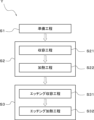
- Processing method X includes a preparation step S1, followed by an annealing step S2.
- the annealing step S2 includes a containing step S21, followed by a heating step S22.
- Processing method X may include a step of performing any processing after the annealing step S2.
- processing method X preferably does not include a step of performing mechanical processing after the annealing step S2.
- the processing method Y includes a preparation step S1 of preparing a SiC substrate 1.
- the preparation step S1 is similar to the preparation step S1 of the processing method X, and therefore a description thereof will be omitted.
- the processing method Y includes an annealing step S2 of annealing the SiC substrate 1 in a crucible 2 made of SiC.
- the annealing step S2 is similar to the annealing step S2 of the processing method X, and therefore a description thereof will be omitted.
- the processing method Y includes an etching step S3 of etching the SiC substrate 1 that has been subjected to the annealing step S2.
- the etching in the etching step S3 is similar to conventional etching in that the microscopic reduction of atoms is repeated, resulting in a macroscopic reduction of atoms. In other words, it is different from the etching in the annealing step S2. At this time, the surface 11 of the SiC substrate 1 is precisely etched, resulting in a SiC substrate 1 with significantly smaller surface roughness.
- the configuration of the component arrangement is substantially the same as that of the annealing step S2, but as shown in FIG. 7, it is preferable to use a large crucible 4 in addition to the SiC substrate 1, crucible 2, and substrate support 3.
- raw material gas phase equilibrium environment refers to an environment in which the raw material gas pressure is such that the SiC substrate and the raw material gas are in approximate phase equilibrium.
- raw material gas phase equilibrium environments include a SiC-C equilibrium vapor pressure environment in which the C element is dominant, and a SiC-Si equilibrium vapor pressure environment in which the Si element is dominant.
- the etching process of this processing method can be said to be a process of etching the SiC substrate in a raw material gas phase equilibrium environment.
- the temperature inside the crucible 2 maintained in the SiC-C equilibrium vapor pressure environment is preferably 1600°C or higher (or more than 1600°C), and preferably 1700°C or higher (or more than 1700°C).
- This temperature is preferably 2000°C or lower (or less than 2000°C), and preferably 1900°C or lower (or less than 1900°C).
- This temperature is preferably lower than the temperature inside the crucible 2 in the annealing step S2.
- the temperature inside the crucible 2, which is maintained in the SiC-Si equilibrium vapor pressure environment, is preferably 1800°C or higher (or more than 1800°C), and preferably 1900°C or higher (or more than 1900°C). This temperature is preferably 2000°C or lower (or less than 2000°C). This temperature is preferably lower than the temperature inside the crucible 2 in the annealing step S2.
- a Si gas source 5 e.g., a Si piece
- a SiC-Si equilibrium vapor pressure environment is formed inside the crucible 2.
- a Si gas source 5 is not placed inside the crucible 2
- a SiC-C equilibrium vapor pressure environment is formed inside the crucible 2.
- a temperature gradient is formed inside the crucible 2.
- the magnitude of this temperature gradient is greater than or equal to 0.1 mm/K and less than or equal to 5 mm/K.
- This temperature gradient is formed in a direction penetrating the SiC substrate 1.
- This temperature gradient is formed in a direction in which the temperature decreases from the C-face 112 toward the Si-face 111.
- the inside of the crucible 2 is maintained in a source gas phase equilibrium environment in the manner described above, so that etching of the Si surface 111 can be performed under suitable conditions.
- the sublimation reaction and the recrystallization reaction are gently balanced with a slight bias toward the sublimation reaction, and the raw material gas gradually sublimes from the Si surface 111.
- the Si surface 111 can be precisely etched, and the surface roughness of the Si surface 111 can be significantly reduced.
- the etching step S3 includes an etching accommodation step S31 for accommodating the SiC substrate 1 in the crucible 2.
- the etching accommodation step S31 is substantially the same as the accommodation step S21 of the processing method X, but includes not arranging the Si gas source 5 in the crucible 2 when etching is performed under a SiC-C equilibrium vapor pressure environment, as shown in FIG. 7, and includes arranging the Si gas source 5 in the crucible 2 when etching the SiC substrate under a SiC-Si equilibrium vapor pressure environment, as shown in FIG. 9.
- the crucible 2 may be the one used in the accommodation step S21, or may be a different one.
- the etching accommodation step S31 may include preparing the crucible 2 that has been subjected to the annealing step S2 with the SiC substrate 1 still accommodated therein, instead of accommodating the SiC substrate 1 in the crucible 2.
- the etching step S3 includes, after the etching accommodation step S31, an etching heating step S32 of heating the crucible 2.
- the etching heating step S32 includes heating the crucible 2 to heat the SiC substrate 1 accommodated inside the crucible 2.
- the etching heating step S32 preferably includes maintaining the inside of the crucible 2 in a SiC-C equilibrium vapor pressure environment.
- the etching heating step S32 preferably includes heating the crucible 2 while evacuating the inside of the crucible 2, and generating a raw material gas from the crucible 2 into the inside of the crucible 2, thereby maintaining the inside of the crucible 2 in a SiC-C equilibrium vapor pressure environment.
- the etching heating step S32 includes heating the crucible 2 and maintaining the temperature inside the crucible 2 at 1600°C or higher (or exceeding 1600°C). This temperature is preferably 1700°C or higher (or exceeding 1700°C). This temperature is 2000°C or lower (or lower than 2000°C). This temperature is preferably 1900°C or lower (or lower than 1900°C). This temperature is preferably lower than the temperature inside the crucible 2 in the heating step S22.
- the etching heating step S32 also preferably includes maintaining the inside of the crucible 2 in a SiC-Si equilibrium vapor pressure environment.
- the etching heating step S32 preferably includes heating the crucible 2 while evacuating the inside of the crucible 2, generating raw material gas from the crucible 2 into the inside of the crucible 2, and generating Si gas from the Si gas source 5 into the inside of the crucible 2, thereby maintaining the inside of the crucible 2 in a SiC-Si equilibrium vapor pressure environment.
- the etching heating step S32 includes heating the crucible 2 and maintaining the temperature inside the crucible 2 at 1800°C or higher (or exceeding 1800°C). This temperature is preferably 1900°C or higher (or exceeding 1900°C). This temperature is 2000°C or lower (or lower than 2000°C). This temperature is preferably lower than the temperature inside the crucible 2 in the heating step S22.
- the etching heating process S32 involves forming a macroscopic flow of the raw material gas inside the crucible 2 by forming a temperature gradient inside the crucible 2 in a direction penetrating the SiC substrate 1.
- the etching heating process S32 involves creating a temperature difference such that the base 21 is at a high temperature and the lid 22 is at a low temperature. This creates a temperature gradient in which the temperature decreases from the C-face 112 side toward the Si-face 111 side, and as a result, the Si-face 111 can be precisely etched.
- the etching heating process S32 involves heating the crucible 2 using a heating furnace as a heat source. This allows the inside of the crucible 2 to be heated from the outside of the crucible 2. In addition, by creating a difference in heating output between the upper and lower parts of the heating furnace, a desired temperature gradient can be formed inside the crucible 2.
- Processing method Y includes a preparation step S1, an annealing step S2, and an etching step S3.
- the annealing step S2 includes a storage step S21 and a heating step S22.
- the etching step S3 includes an etching storage step S31 and an etching heating step S32.
- Processing method Y may include a step of performing any processing after the etching step S3.
- processing method Y preferably does not include a step of performing mechanical processing after the etching step S3.
- ⁇ Treatment method Z> A third preferred embodiment of the present processing method will be described in detail with reference to Fig. 11.
- Fig. 11 the same components as those shown in Figs. 1 to 10 are designated by the same reference numerals.
- processing method Z the third preferred embodiment of the present processing method will be referred to as processing method Z.
- the processing method Z includes a preparation step S1 of preparing a SiC substrate 1.
- the preparation step S1 is similar to the preparation step S1 of the processing method Y, and therefore a description thereof will be omitted.
- the processing method Z includes an annealing step S2 of annealing the SiC substrate 1 in a crucible 2 made of SiC.
- the annealing step S2 is similar to the annealing step S2 of the processing method Y, and therefore a description thereof will be omitted.
- the processing method Z includes a first etching step S4 for etching the SiC substrate 1 that has been subjected to the annealing step S2.
- the first etching step S4 is substantially similar to the etching step S3 of the processing method Y, but the inside of the crucible 2 is maintained in a SiC-C equilibrium vapor pressure environment.
- the processing method Z includes a second etching step S5 for further etching the SiC substrate 1 that has been subjected to the first etching step S4.
- the second etching step S5 is substantially similar to the etching step S3 of the processing method Y, but the inside of the crucible 2 is maintained in a SiC-Si equilibrium vapor pressure environment.
- the second etching step S5 has a second etching accommodation step S51 of accommodating the SiC substrate 1 inside the crucible 2.
- the second etching accommodation step S51 is substantially similar to the etching accommodation step S31 of the processing method Y, but includes disposing a Si gas source 5 inside the crucible 2 as shown in FIG.
- the second etching step S5 includes a second etching heating step S52 for heating the crucible 2 after the second etching accommodation step S51.
- the second etching heating step S52 is substantially similar to the etching heating step S32 of the processing method Y, but includes maintaining the inside of the crucible 2 in a SiC-Si equilibrium vapor pressure environment.
- the SiC substrate 1 is etched in a SiC-C equilibrium vapor pressure environment in the first etching step S4, and then the SiC substrate 1 is etched in a SiC-Si equilibrium vapor pressure environment in the second etching step S5, thereby etching the Si surface 111 more precisely and further reducing the surface roughness of the Si surface (in particular, the macrostep bunching of the Si surface can be resolved).
- Processing method Z includes a preparation step S1, an annealing step S2, a first etching step S4, and a second etching step S5.
- the annealing step S2 includes a storage step S21 and a heating step S22.
- the first etching step S4 includes a first etching storage step S41 and a first etching heating step S42.
- the second etching step S5 includes a second etching storage step S51 and a second etching heating step S52.
- Processing method Z may include a step of performing any processing after the second etching step S5.
- processing method Z preferably does not include a step of performing mechanical processing after the second etching step S5.
- the processing method V includes a preparation step S1 of preparing a SiC substrate 1.
- the preparation step S1 is similar to the preparation step S1 of the processing method Z, and therefore a description thereof will be omitted.
- the processing method V includes an annealing step S2 of annealing the SiC substrate 1 in a crucible 2 made of SiC.
- the annealing step S2 is similar to the annealing step S2 of the processing method Z, and therefore a description thereof will be omitted.
- the processing method V includes an etching step S3 for etching the SiC substrate 1 that has been subjected to the annealing step S2.
- the etching step S3 is similar to the etching step S3 of the processing method Y, and therefore a description thereof will be omitted.
- the processing method V preferably includes a first etching step S4 and a second etching step S5 in this order as the etching step S3.
- the first etching step S4 and the second etching step S5 are similar to the first etching step S4 and the second etching step S5 of the processing method Z, and therefore a description thereof will be omitted.
- the processing method V includes a growing step S6 of growing a SiC substrate 1 that has been subjected to the etching step S3.
- the growth in growth step S6 is similar to conventional growth in that a macroscopic increase in atoms occurs as a result of repeated increases in microscopic atoms. In other words, it differs from the growth in annealing step S2. At this time, the surface 11 of the SiC substrate 1 grows precisely, resulting in a SiC substrate 1 with significantly smaller surface roughness.
- the configuration of the component arrangement is the same as that in the etching process S3.
- the inside of the crucible 2 is maintained in a raw material gas phase equilibrium environment.
- the growth process of this processing method can be said to be a process of growing a SiC substrate in a raw material gas phase equilibrium environment.
- the temperature inside the crucible 2 maintained in the SiC-C equilibrium vapor pressure environment is preferably 1600°C or higher (or more than 1600°C), and preferably 1700°C or higher (or more than 1700°C).
- This temperature is preferably 2000°C or lower (or less than 2000°C), and preferably 1900°C or lower (or less than 1900°C).
- This temperature is preferably lower than the temperature inside the crucible 2 in the annealing step S2.
- the temperature inside the crucible 2, which is maintained in the SiC-Si equilibrium vapor pressure environment, is preferably 1800°C or higher (or more than 1800°C), and preferably 1900°C or higher (or more than 1900°C). This temperature is preferably 2000°C or lower (or less than 2000°C). This temperature is preferably lower than the temperature inside the crucible 2 in the annealing step S2.
- a temperature gradient is formed inside the crucible 2.
- the magnitude of this temperature gradient is greater than or equal to 0.1 mm/K and less than or equal to 5 mm/K.
- This temperature gradient is formed in a direction penetrating the SiC substrate 1.
- This temperature gradient is formed in a direction in which the temperature decreases from the Si surface 111 toward the C surface 112.
- the inside of the crucible 2 is maintained in a source gas phase equilibrium environment in the manner described above, so that the growth of the Si surface 111 can be carried out under favorable conditions.
- the Si surface 111 can be grown precisely, and an increase in the surface roughness of the Si surface 111 can be significantly suppressed.
- the growth step S6 includes a growth accommodation step S61 in which the SiC substrate 1 is accommodated in the crucible 2.
- the growth accommodation step S61 is the same as the etching accommodation step S31 of the processing method Y.
- the crucible 2 may be the one used in the accommodation step S21, the one used in the etching accommodation step S31, or a different one.
- the growth accommodation step S61 may include preparing the crucible 2 that has been subjected to the etching step S3 with the SiC substrate 1 still accommodated therein.
- the growth step S6 includes, after the growth accommodation step S61, a growth heating step S62 of heating the crucible 2.
- the growth heating step S62 includes heating the crucible 2 to heat the SiC substrate 1 accommodated inside the crucible 2.
- the growth heating step S62 includes heating the crucible 2 and maintaining the temperature inside the crucible 2 at 1600°C or higher (or exceeding 1600°C). This temperature is preferably 1700°C or higher (or exceeding 1700°C). This temperature is 2000°C or lower (or lower than 2000°C). This temperature is preferably 1900°C or lower (or lower than 1900°C). This temperature is preferably lower than the temperature inside the crucible 2 in the heating step S22.
- the growth heating step S62 also preferably includes maintaining the inside of the crucible 2 in a SiC-Si equilibrium vapor pressure environment.
- the growth heating step S62 preferably includes heating the crucible 2 while evacuating the inside of the crucible 2, generating source gas from the crucible 2 into the inside of the crucible 2, and generating Si gas from the Si gas source 5 into the inside of the crucible 2, thereby maintaining the inside of the crucible 2 in a SiC-Si equilibrium vapor pressure environment.
- the growth heating step S62 involves forming a macroscopic flow of the source gas inside the crucible 2 by forming a temperature gradient inside the crucible 2 in a direction penetrating the SiC substrate 1.
- the growth heating step S62 involves creating a temperature difference such that the base 21 is at a low temperature and the lid 22 is at a high temperature. This creates a temperature gradient in which the temperature decreases from the Si face 111 side toward the C face 112 side, and as a result, the Si face 111 can be grown precisely.
- the growth heating step S62 includes heating the crucible 2 using a heating furnace as a heat source. This allows the inside of the crucible 2 to be heated from the outside of the crucible 2. In addition, by providing a difference in heating output between the upper and lower parts of the heating furnace, a desired temperature gradient can be formed inside the crucible 2.
- Processing method V includes a preparation step S1, followed by an annealing step S2, followed by an etching step S3, followed by a growth step S6.
- the annealing step S2 includes a storage step S21, followed by a heating step S22.
- the etching step S3 includes an etching storage step S31, followed by an etching heating step S32.
- the growth step S6 includes a growth storage step S61, followed by a growth heating step S62.
- Processing method V may include a step of performing any processing after the growth step S6.
- processing method V preferably does not include a step of performing mechanical processing after the growth step S6.
- ⁇ Processing method W> The fifth preferred embodiment of the present processing method will be described in detail with reference to Fig. 13.
- Fig. 13 the same components as those shown in Figs. 1 to 12 are designated by the same reference numerals.
- processing method W the fifth preferred embodiment of the present processing method will be referred to as processing method W.
- the processing method W includes a preparation step S1 of preparing a SiC substrate 1.
- the preparation step S1 is similar to the preparation step S1 of the processing method V, and therefore a description thereof will be omitted.
- the processing method W includes an annealing step S2 of annealing the SiC substrate 1 in a crucible 2 made of SiC.
- the annealing step S2 is similar to the annealing step S2 of the processing method V, and therefore a description thereof will be omitted.
- the processing method W includes a first etching step S4 of etching the SiC substrate 1 that has been subjected to the annealing step S2.
- the first etching step S4 is similar to the first etching step S4 of the processing method Z, and therefore a description thereof will be omitted.
- the processing method W includes a second etching step S5 for further etching the SiC substrate 1 that has been subjected to the first etching step S4.
- the second etching step S5 is similar to the second etching step S5 of the processing method Z, and therefore a description thereof will be omitted.
- the processing method W includes a first growth step S7 for growing the SiC substrate 1 that has been subjected to the second etching step S5.
- the first growth step S7 is substantially similar to the growth step S6 of the processing method V, but the inside of the crucible 2 is maintained in a SiC-C equilibrium vapor pressure environment.
- the first growth step S7 includes a first growth accommodation step S71 in which the SiC substrate 1 is accommodated inside the crucible 2.
- the first growth accommodation step S71 is substantially similar to the growth accommodation step S61 of the processing method V, but includes the fact that the Si gas source 5 is not disposed inside the crucible 2, as shown in FIG.
- the first growth step S7 includes a first growth heating step S72 of heating the crucible 2 after the first growth accommodation step S71.
- the first growth heating step S72 is substantially similar to the growth heating step S62 of the processing method V, but includes maintaining the inside of the crucible 2 in a SiC-C equilibrium vapor pressure environment.
- the processing method W includes a second growth step S8 in which the SiC substrate 1 that has been subjected to the first growth step S7 is further grown.
- the second growth step S8 is substantially similar to the growth step S6 of the processing method V, but the inside of the crucible 2 is maintained in a SiC-Si equilibrium vapor pressure environment.
- the second growth step S8 includes a second growth accommodation step S81 in which the SiC substrate 1 is accommodated inside the crucible 2.
- the second growth accommodation step S81 is substantially similar to the growth accommodation step S61 of the processing method V, but includes disposing a Si gas source 5 inside the crucible 2, as shown in FIG.
- the second growth step S8 includes a second growth heating step S82 of heating the crucible 2 after the second growth accommodation step S81.
- the second growth heating step S82 is substantially similar to the growth heating step S62 of the processing method V, but includes maintaining the inside of the crucible 2 in a SiC-Si equilibrium vapor pressure environment.
- the SiC substrate 1 is etched in a SiC-Si equilibrium vapor pressure environment in the second etching step S5, and then the SiC substrate 1 is grown in a SiC-C equilibrium vapor pressure environment in the first growth step S7, thereby significantly suppressing the inheritance of basal plane dislocations (BPDs) in the growth layer.
- BPDs basal plane dislocations
- the SiC substrate 1 is grown in a SiC-C equilibrium vapor pressure environment in the first growth step S7 in the above-described form, and then the SiC substrate 1 is grown in a SiC-Si equilibrium vapor pressure environment in the second growth step S8, thereby significantly reducing the surface roughness of the Si surface (in particular, the macro-step bunching of the Si surface can be resolved).
- processing method W can process a SiC substrate in any state into a SiC substrate suitable for manufacturing SiC semiconductor devices, with significantly reduced surface roughness, significantly reduced BPD, and significantly removed damaged layers that cause in-grown stacking faults (IGSFs).
- IGSFs in-grown stacking faults
- the flow of the processing method W is as shown in FIG. 13.
- the processing method Z includes performing a preparation step S1, then performing an annealing step S2, then performing a first etching step S4, then performing a second etching step S5, then performing a first growth step S7, and then performing a second growth step S8.
- the annealing step S2 includes performing a storage step S21, then performing a heating step S22.
- the first etching step S4 includes performing a first etching storage step S41, then performing a first etching heating step S42.
- the second etching step S5 includes performing a second etching storage step S51, then performing a second etching heating step S52.
- the first growth step S7 includes performing a first growth storage step S71, then performing a first growth heating step S72.
- the second growth step S8 includes performing a second growth storage step S81, then performing a second growth heating step S82.
- the processing method W may include a step of performing any processing after the second growth step S8.
- it is preferable that processing method W does not include a step of performing mechanical processing after the second growth step S8.
- Processing method X was carried out according to the following steps:
- ⁇ Preparation step S1> A substrate for which the following characteristics were measured was prepared as SiC substrate 1. In order to eliminate the influence of the measurement of SiC substrate 1 on surface 11, SiC substrate 1 was cleaned with a chemical solution.
- ⁇ Storage step S21> As shown in FIG. 6, a SiC substrate 1 was placed inside a crucible 2 made of polycrystalline SiC.
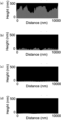
- Figure 14 shows the contour lines based on the AFM image (10 ⁇ m x 10 ⁇ m).
- (a) is the SiC substrate 1 prepared in the preparation step S1
- (b) is the SiC substrate 1 that has undergone the annealing step S2.
- a comparison of the contour line shapes shows that the surface roughness of the Si surface 111 has been reduced.
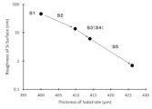
- Figure 15 shows the relationship between the arithmetic mean roughness Ra of the Si surface 111 and the substrate thickness.
- the arithmetic mean roughness Ra of the Si surface 111 was reduced from 46.2 nm to 13.7 nm after undergoing the annealing step S2.
- the substrate thickness of the SiC substrate 1 increased from 400.0 ⁇ m to 409.8 ⁇ m after undergoing the annealing step S2. This shows that the surface roughness of the Si surface 111 was reduced while the substrate thickness of the SiC substrate 1 was almost maintained. It is believed that due to the temperature difference conditions, the Si surface 111 was etched and at the same time, the C surface 112 grew. It is also believed that the amount of etching on the Si surface 111 was approximately the same as or smaller than the amount of growth of the C surface 112.
- Processing method X was carried out according to the following steps:
- ⁇ Preparation step S1> A substrate for which the following characteristics were measured was prepared as SiC substrate 1. In order to eliminate the influence of the measurement of SiC substrate 1 on surface 11, SiC substrate 1 was cleaned with a chemical solution.
- ⁇ Storage step S21> As shown in FIG. 6, a SiC substrate 1 was placed inside a crucible 2 made of polycrystalline SiC.
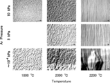
- Ar gas Pressure vacuum (up to 10 ⁇ 4 kPa), 5 kPa, or 10 kPa
- Temperature 1800° C., 2000° C., or 2200° C.
- Temperature difference base 21 is at high temperature, and lid 22 is at low temperature
- Figure 16 shows laser microscope images of the Si surface 111 of the SiC substrate processed under each set of conditions. It was found that the scale of the irregularities on the surface was smaller when the pressure was 5 kPa or higher, compared to when the pressure was a vacuum. In addition, it was found that when the temperature was 2200°C or higher, a step-terrace structure appeared on the surface, i.e., the surface shape was regularized.
- the arithmetic mean height Sa was 70 nm when the pressure was in a vacuum and 153 nm when the pressure was 10 kPa when the temperature was 1800°C, 174 nm when the pressure was in a vacuum, 71 nm when the pressure was 5 kPa, and 86 nm when the pressure was 10 kPa when the temperature was 2000°C, and 242 nm when the pressure was in a vacuum, 56 nm when the pressure was 5 kPa, and 54 nm when the pressure was 10 kPa when the temperature was 2200°C.
- Comparison of the arithmetic mean height Sa showed that the surface roughness of the Si surface 111 was clearly reduced when the pressure was 5 kPa or higher. In addition, it was found that the surface roughness of the Si surface 111 was significantly reduced when the temperature was 2000°C or higher, and was even more significantly reduced when the temperature was 2200°C or higher.
- processing method Y was carried out according to the following steps.
- SiC substrate 1 was washed with a chemical solution.
- ⁇ Etching heating step S32> The SiC substrate 1 was heated under the following conditions. At this time, the inside of the crucible 2 was in a SiC-C equilibrium vapor pressure environment.
- (c) shows the SiC substrate 1 that has undergone the etching process S3.
- a comparison of the contour line shapes shows that the surface roughness of the Si surface 111 has been further reduced.
- the arithmetic mean roughness Ra of the Si surface 111 was reduced from 13.7 nm to 6.1 nm after the etching process S3.
- the substrate thickness of the SiC substrate 1 increased from 409.8 ⁇ m to 414.0 ⁇ m after the etching process S3. This shows that the surface roughness of the Si surface 111 was reduced while the substrate thickness of the SiC substrate 1 was almost maintained. Due to the temperature difference conditions, it is believed that the Si surface 111 was etched and, at the same time, the C surface 112 grew. In addition, it is believed that the amount of etching on the Si surface 111 was approximately the same as or smaller than the amount of growth of the C surface 112.
- Processing Method Z was carried out according to the following steps. However, the first etching step S4 of Processing Method Z was the same as the etching step S3 of Example 2. In addition, in order to eliminate the effect on the surface 11 caused by the measurement of the SiC substrate 1, the SiC substrate 1 was washed with a chemical solution.
- (d) shows the SiC substrate 1 that has undergone the second etching step S5.
- a comparison of the contour line shapes shows that the surface roughness of the Si surface 111 has been further reduced.
- the arithmetic mean roughness Ra of the Si surface 111 was reduced from 6.1 nm to 0.7 nm after the second etching step S5.
- the substrate thickness of the SiC substrate 1 increased from 414.0 ⁇ m to 426.1 ⁇ m after the second etching step S5. This shows that the surface roughness of the Si surface 111 was reduced while the substrate thickness of the SiC substrate 1 was almost maintained. Due to the temperature difference conditions, it is believed that the Si surface 111 was etched and, at the same time, the C surface 112 grew. In addition, it is believed that the amount of etching of the Si surface 111 was approximately the same as or smaller than the amount of growth of the C surface 112.
- Processing method V was carried out according to the following steps:
- ⁇ Preparation step S1> A substrate for which the following characteristics were measured was prepared as SiC substrate 1. In order to eliminate the influence of the measurement of SiC substrate 1 on surface 11, SiC substrate 1 was cleaned with a chemical solution.
- ⁇ Storage step S21> As shown in FIG. 6, a SiC substrate 1 was placed inside a crucible 2 made of polycrystalline SiC.
- Inlet gas Ar gas Pressure: 10 kPa Temperature: 2200°C Temperature difference: base 21 is high temperature, lid 22 is low temperature Time: 1 hour
- ⁇ Growth heating step S62> The SiC substrate 1 was heated under the following conditions. At this time, the inside of the crucible 2 was in a SiC-C equilibrium vapor pressure environment.
- the arithmetic mean roughness Ra of the Si surface 111 was less than 5 nm.
- the photoluminescence image of the Si surface 111 was as shown on the right in Fig. 17.
- Processing method S2 Annealing process
- S21 Housing process
- Heating process 1 SiC substrate 11: Surface 111: Si surface 112: C surface 12:
- Process-affected layer 2 Crucible 21: Base 22: Lid 3: Substrate support d: Depth
Landscapes
- Chemical & Material Sciences (AREA)
- Engineering & Computer Science (AREA)
- Crystallography & Structural Chemistry (AREA)
- Materials Engineering (AREA)
- Metallurgy (AREA)
- Organic Chemistry (AREA)
- Physics & Mathematics (AREA)
- Plasma & Fusion (AREA)
- Inorganic Chemistry (AREA)
- Crystals, And After-Treatments Of Crystals (AREA)
- Drying Of Semiconductors (AREA)
Abstract
L'invention concerne un nouveau procédé de traitement d'un substrat de SiC. L'invention concerne un procédé de traitement d'un substrat de SiC, le procédé comprenant une étape de recuit S1 pour chauffer un substrat de SiC 1 à l'intérieur d'un creuset 2 composé de SiC, dans l'étape de recuit S1, l'intérieur du creuset 2 étant maintenu dans un environnement de gaz inerte.
Priority Applications (1)
| Application Number | Priority Date | Filing Date | Title |
|---|---|---|---|
| CN202480054755.1A CN121729530A (zh) | 2023-09-15 | 2024-08-30 | SiC基板的处理方法、去除SiC基板的加工变质层的方法及降低SiC基板的表面粗糙度的方法 |
Applications Claiming Priority (2)
| Application Number | Priority Date | Filing Date | Title |
|---|---|---|---|
| JP2023150566 | 2023-09-15 | ||
| JP2023-150566 | 2023-09-15 |
Publications (1)
| Publication Number | Publication Date |
|---|---|
| WO2025057770A1 true WO2025057770A1 (fr) | 2025-03-20 |
Family
ID=95021243
Family Applications (1)
| Application Number | Title | Priority Date | Filing Date |
|---|---|---|---|
| PCT/JP2024/031151 Pending WO2025057770A1 (fr) | 2023-09-15 | 2024-08-30 | PROCÉDÉ DE TRAITEMENT DE SUBSTRAT DE SiC, PROCÉDÉ D'ÉLIMINATION DE COUCHE AFFECTÉE PAR LE TRAITEMENT DE SUBSTRAT DE SiC, ET PROCÉDÉ DE RÉDUCTION DE RUGOSITÉ DE SURFACE DE SUBSTRAT DE SiC |
Country Status (3)
| Country | Link |
|---|---|
| CN (1) | CN121729530A (fr) |
| TW (1) | TW202519714A (fr) |
| WO (1) | WO2025057770A1 (fr) |
Citations (4)
| Publication number | Priority date | Publication date | Assignee | Title |
|---|---|---|---|---|
| WO2015151413A1 (fr) * | 2014-03-31 | 2015-10-08 | 東洋炭素株式会社 | Procédé de traitement de surface pour substrats sic, substrat sic, et procédé de fabrication de composants à semi-conducteur |
| WO2020179793A1 (fr) | 2019-03-05 | 2020-09-10 | 学校法人関西学院 | PROCÉDÉ ET DISPOSITIF DE FABRICATION D'UN SUBSTRAT EN SiC ET PROCÉDÉ DE RÉDUCTION DE LA CONCENTRATION DE MACRO-SURÉPAISSEURS DU SUBSTRAT EN SiC |
| WO2020179794A1 (fr) | 2019-03-05 | 2020-09-10 | 学校法人関西学院 | PROCÉDÉ DE FABRICATION ET DISPOSITIF DE FABRICATION DE SUBSTRAT DE SiC, ET PROCÉDÉ DE RÉDUCTION DE COUCHE AFFECTÉE LORS DU FAÇONNAGE DANS UN SUBSTRAT DE SiC |
| WO2020179795A1 (fr) * | 2019-03-05 | 2020-09-10 | 学校法人関西学院 | PROCÉDÉ ET APPAREIL POUR PRODUCTION D'UN SUBSTRAT EN SiC |
-
2024
- 2024-08-30 CN CN202480054755.1A patent/CN121729530A/zh active Pending
- 2024-08-30 WO PCT/JP2024/031151 patent/WO2025057770A1/fr active Pending
- 2024-09-16 TW TW113135023A patent/TW202519714A/zh unknown
Patent Citations (4)
| Publication number | Priority date | Publication date | Assignee | Title |
|---|---|---|---|---|
| WO2015151413A1 (fr) * | 2014-03-31 | 2015-10-08 | 東洋炭素株式会社 | Procédé de traitement de surface pour substrats sic, substrat sic, et procédé de fabrication de composants à semi-conducteur |
| WO2020179793A1 (fr) | 2019-03-05 | 2020-09-10 | 学校法人関西学院 | PROCÉDÉ ET DISPOSITIF DE FABRICATION D'UN SUBSTRAT EN SiC ET PROCÉDÉ DE RÉDUCTION DE LA CONCENTRATION DE MACRO-SURÉPAISSEURS DU SUBSTRAT EN SiC |
| WO2020179794A1 (fr) | 2019-03-05 | 2020-09-10 | 学校法人関西学院 | PROCÉDÉ DE FABRICATION ET DISPOSITIF DE FABRICATION DE SUBSTRAT DE SiC, ET PROCÉDÉ DE RÉDUCTION DE COUCHE AFFECTÉE LORS DU FAÇONNAGE DANS UN SUBSTRAT DE SiC |
| WO2020179795A1 (fr) * | 2019-03-05 | 2020-09-10 | 学校法人関西学院 | PROCÉDÉ ET APPAREIL POUR PRODUCTION D'UN SUBSTRAT EN SiC |
Also Published As
| Publication number | Publication date |
|---|---|
| CN121729530A (zh) | 2026-03-24 |
| TW202519714A (zh) | 2025-05-16 |
Similar Documents
| Publication | Publication Date | Title |
|---|---|---|
| JP5304713B2 (ja) | 炭化珪素単結晶基板、炭化珪素エピタキシャルウェハ、及び薄膜エピタキシャルウェハ | |
| JP7578870B2 (ja) | SiC基板、SiCエピタキシャル基板、SiCインゴット及びこれらの製造方法 | |
| JP7751782B2 (ja) | SiC種結晶及びその製造方法、当該SiC種結晶を成長させたSiCインゴット及びその製造方法、並びに、当該SiCインゴットより製造されるSiCウェハ、エピタキシャル膜付きSiCウェハ及びこれらの製造方法 | |
| TWI899095B (zh) | 碳化矽基板的製造方法 | |
| JP5569112B2 (ja) | 炭化珪素単結晶ウェハの製造方法及びこの方法で得られた炭化珪素単結晶ウェハ | |
| JP7651786B2 (ja) | 半導体基板の製造方法、その製造装置、及び、エピタキシャル成長方法 | |
| WO2020179795A1 (fr) | PROCÉDÉ ET APPAREIL POUR PRODUCTION D'UN SUBSTRAT EN SiC | |
| CN114207195B (zh) | SiC衬底的制造方法及其制造装置和减少SiC衬底的宏观台阶聚束的方法 | |
| CN114423889B (zh) | SiC单晶的制造方法、SiC单晶的制造装置以及SiC单晶晶片 | |
| WO2020179794A1 (fr) | PROCÉDÉ DE FABRICATION ET DISPOSITIF DE FABRICATION DE SUBSTRAT DE SiC, ET PROCÉDÉ DE RÉDUCTION DE COUCHE AFFECTÉE LORS DU FAÇONNAGE DANS UN SUBSTRAT DE SiC | |
| JP6052465B2 (ja) | エピタキシャル炭化珪素ウエハの製造方法 | |
| JP4494856B2 (ja) | 炭化珪素単結晶成長用種結晶とその製造方法及びそれを用いた結晶成長方法 | |
| JP7678246B2 (ja) | 半導体基板の製造方法及び半導体基板の製造装置 | |
| JP7758909B2 (ja) | 窒化アルミニウム基板の製造方法、窒化アルミニウム基板、及び、窒化アルミニウム層を形成する方法 | |
| JP7769846B2 (ja) | 半導体基板の製造方法、半導体基板、及び、成長層におけるクラックの発生を抑制する方法 | |
| JP7557701B2 (ja) | SiC基板の製造方法、その製造装置、及び、エピタキシャル成長方法 | |
| WO2025057770A1 (fr) | PROCÉDÉ DE TRAITEMENT DE SUBSTRAT DE SiC, PROCÉDÉ D'ÉLIMINATION DE COUCHE AFFECTÉE PAR LE TRAITEMENT DE SUBSTRAT DE SiC, ET PROCÉDÉ DE RÉDUCTION DE RUGOSITÉ DE SURFACE DE SUBSTRAT DE SiC | |
| WO2025057772A1 (fr) | Procédé de traitement de substrat en carbure de silicium, procédé d'élimination de couche affectée par le traitement de substrat en carbure de silicium, et procédé de réduction de rugosité de surface de substrat en carbure de silicium | |
| JP5135545B2 (ja) | 炭化珪素単結晶インゴット育成用種結晶及びその製造方法 | |
| JP7569850B2 (ja) | 単結晶窒化アルミニウム基板の表面の構造的損傷を低減させる方法およびその方法によって製造される単結晶窒化アルミニウム基板 | |
| JP7758908B2 (ja) | 半導体基板の製造方法、半導体基板、及び、成長層を形成する方法 | |
| JP2024539552A (ja) | 一時的な保護酸化物層を有するSiC種結晶を用いた、品質の向上したSiCバルク単結晶の製造方法、及び保護酸化物層を有するSiC種結晶 | |
| WO2026071136A1 (fr) | PROCÉDÉ DE PRODUCTION D'UN SUBSTRAT DE SiC ET SUBSTRAT DE SiC AYANT UNE COUCHE DE CROISSANCE |
Legal Events
| Date | Code | Title | Description |
|---|---|---|---|
| 121 | Ep: the epo has been informed by wipo that ep was designated in this application |
Ref document number: 24865272 Country of ref document: EP Kind code of ref document: A1 |
|
| ENP | Entry into the national phase |
Ref document number: 2025545604 Country of ref document: JP Kind code of ref document: A |
|
| WWE | Wipo information: entry into national phase |
Ref document number: 2025545604 Country of ref document: JP |
|
| WWE | Wipo information: entry into national phase |
Ref document number: 2024865272 Country of ref document: EP |