WO2025062637A1 - Dispositif à semi-conducteur - Google Patents
Dispositif à semi-conducteur Download PDFInfo
- Publication number
- WO2025062637A1 WO2025062637A1 PCT/JP2023/034522 JP2023034522W WO2025062637A1 WO 2025062637 A1 WO2025062637 A1 WO 2025062637A1 JP 2023034522 W JP2023034522 W JP 2023034522W WO 2025062637 A1 WO2025062637 A1 WO 2025062637A1
- Authority
- WO
- WIPO (PCT)
- Prior art keywords
- semiconductor device
- electrode
- conductive portion
- substrate
- recess
- Prior art date
- Legal status (The legal status is an assumption and is not a legal conclusion. Google has not performed a legal analysis and makes no representation as to the accuracy of the status listed.)
- Pending
Links
Images


Classifications
-
- H—ELECTRICITY
- H10—SEMICONDUCTOR DEVICES; ELECTRIC SOLID-STATE DEVICES NOT OTHERWISE PROVIDED FOR
- H10W—GENERIC PACKAGES, INTERCONNECTIONS, CONNECTORS OR OTHER CONSTRUCTIONAL DETAILS OF DEVICES COVERED BY CLASS H10
- H10W70/00—Package substrates; Interposers; Redistribution layers [RDL]
- H10W70/60—Insulating or insulated package substrates; Interposers; Redistribution layers
Definitions
- This disclosure relates to a semiconductor device.
- JP 2013-89948 A there is known a semiconductor device that uses flip-chip mounting in which a mounting substrate is connected to an electrode of a semiconductor substrate so that the back surface of the semiconductor substrate faces the mounting substrate (see, for example, JP 2013-89948 A).
- the semiconductor substrate has a guard ring as an electric field strength mitigation section that mitigates the high electric field generated in the active region.
- the semiconductor device includes a semiconductor substrate and a mounting substrate.
- the semiconductor substrate has a first surface.
- the mounting substrate has a main surface. The main surface faces the first surface.
- An electric field strength mitigation portion and an electrode are formed on the first surface.
- the electrode is connected to the mounting substrate.
- a recess is formed on the main surface. The recess is disposed at a position overlapping the electric field strength mitigation portion in a plan view of the first surface.
- 1 is a schematic cross-sectional view of a semiconductor device according to a first embodiment
- 2 is a schematic bottom view of a semiconductor substrate in the semiconductor device according to the first embodiment
- 1 is a schematic plan view of a mounting substrate in a semiconductor device according to a first embodiment
- 4 is a schematic cross-sectional view taken along line IV-IV in FIG. 3.
- 4 is a schematic cross-sectional view taken along line VV in FIG. 3.
- 3 is a schematic partial cross-sectional view of a recess in the semiconductor device according to the first embodiment
- 10 is a schematic partial cross-sectional view of a modified example of a recess in the semiconductor device according to the first embodiment.
- FIG. 10 is a schematic partial cross-sectional view of a modified example of a recess in the semiconductor device according to the first embodiment.
- FIG. 10 is a schematic partial cross-sectional view of a modified example of a recess in the semiconductor device according to the first embodiment.
- FIG. 2 is a schematic plan view showing a conductive portion in the semiconductor device according to the first embodiment;
- 11 is a schematic cross-sectional view taken along line XI-XI in FIG. 10 .
- FIG. 17 is a schematic cross-sectional view taken along line XVII-XVII in FIG. 16.
- FIG. 11 is a schematic cross-sectional view of a semiconductor device according to a third embodiment.
- FIG. 11 is a schematic cross-sectional view of a semiconductor device according to a fourth embodiment.
- FIG. 13 is a schematic cross-sectional view of a semiconductor device according to a fifth embodiment.
- FIG. 13 is a schematic cross-sectional view of a modified example of the semiconductor device according to the fifth embodiment.
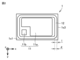
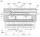
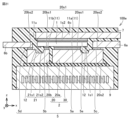
- FIG 1 is a schematic cross-sectional view of a semiconductor device 100a according to a first embodiment.
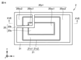
- FIG 2 is a schematic bottom view of a semiconductor substrate 1 in the semiconductor device 100a according to the first embodiment.
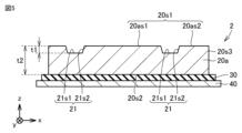
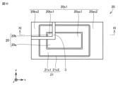
- FIG 3 is a schematic plan view of a mounting substrate 2 in the semiconductor device 100a according to the first embodiment.
- FIG 4 is a schematic cross-sectional view taken along line IV-IV in FIG 3.
- FIG 5 is a schematic cross-sectional view taken along line V-V in FIG 3.
- FIG 6 is a schematic partial cross-sectional view of an electric field intensity mitigating portion 12 and a recess 21 in the semiconductor device 100a according to the first embodiment.
- the semiconductor device 100a shown in Figures 1 to 6 is, for example, a power semiconductor device 100a, and mainly comprises a semiconductor substrate 1, a mounting substrate 2, a joint 5, a wiring circuit 6, and a sealing resin 7.
- the joint 5 includes a first joint 5a, a second joint 5b, a third joint 5c, a fourth joint 5d, and a fifth joint 5e.
- the wiring circuit 6 includes a first wiring circuit 6a, a second wiring circuit 6b, and a third wiring circuit 6c.
- the semiconductor substrate 1 has a first surface 1s1, a second surface 1s2, and a third surface 1s3.
- the first surface 1s1 is the surface facing the main surface 20s1 of the mounting substrate 2.
- the second surface 1s2 is the surface opposite the first surface 1s1.
- the third surface 1s3 connects the first surface 1s1 and the second surface 1s2.
- the first surface 1s1 is the back surface of the semiconductor substrate 1.
- the second surface 1s2 is the front surface of the semiconductor substrate 1.
- the third surface 1s3 is the side surface of the semiconductor substrate 1.
- the first surface 1s1 and the second surface 1s2 extend in the x direction and the y direction perpendicular to the x direction.
- the x direction is the direction in which the wiring circuit extends.
- the y direction is perpendicular to the x direction.
- the z direction is the thickness direction of the semiconductor substrate 1.
- the normal direction of the first surface 1s1 is the z direction.
- the second surface 1s2 faces the +z direction.
- the first surface 1s1 faces the -z direction.
- the shape of the electric field strength mitigation section 12 does not have to be annular.
- the electric field strength mitigation section 12 may be a termination structure called a JTE (Junction Termination Extension) structure.
- the electric field strength mitigation section 12 may be, for example, a p-type region formed by ion implantation.
- the electrode 11 includes a first electrode 11a and a second electrode 11b.
- the first electrode 11a is a main electrode.
- a main current flows through the main electrode.
- the second electrode 11b is a control electrode.
- the control electrode controls the main current.
- the first electrode 11a and the second electrode 11b are disposed spaced apart from each other on the first surface 1s1.
- the first electrode 11a is connected to the mounting substrate 2 via the first joint 5a.
- the second electrode 11b is connected to the mounting substrate 2 via the second joint 5b.
- an upper electrode 11u is formed on the second surface 1s2 of the semiconductor substrate 1.
- a main current flows through the upper electrode 11u.
- a third wiring circuit 6c is connected to the upper electrode 11u via a fifth joint 5e.
- the third wiring circuit 6c extends in the x-direction.
- the semiconductor substrate 1 is a so-called power semiconductor substrate 1 that controls power. Any material may be used as the material for forming the semiconductor substrate 1. Materials such as silicon (Si), silicon carbide (SiC), gallium nitride (GaN), and gallium oxide (GaO) may be used as the material for forming the semiconductor substrate 1.
- the material constituting the electrode 11 is preferably a material having high electrical and thermal conductivity.
- the material constituting the electrode 11 may include, for example, any of aluminum (Al), an aluminum alloy, copper (Cu), and a copper alloy.
- the electrode 11 may have a two-layer structure of Al/Cu, or a multi-layer structure including any of gold (Au) and silver (Ag).
- the electrode 11 may include a diffusion prevention layer.
- the diffusion prevention layer may include, for example, titanium (Ti) or the like.
- Nickel (Ni) silicide may be used as an underlayer for the electrode 11 to make ohmic contact with the semiconductor substrate 1.
- the electrode 11 may include a thin surface layer to prevent oxidation of the electrode 11 or to improve its bonding properties.
- the material constituting the surface layer is, for example, a precious metal such as gold.
- the electrodes 11 there are no particular restrictions on the electrodes 11.
- the locations of the first electrode 11a and the second electrode 11b there are no particular restrictions on the locations of the first electrode 11a and the second electrode 11b.
- the second electrode 11b may be disposed as a control electrode in a corner on the first surface 1s1, but it may also be disposed in the center of the first surface 1s1.
- the shape of the second electrode 11b may be any shape.
- the shape of the second electrode 11b may be a rectangle as shown in FIG. 2, or may be a circle, an ellipse, or a combination of an ellipse and a rectangle.
- the shape of the second electrode 11b may be a hexagon.
- the mounting substrate 2 has a conductive portion 20, a thermally conductive insulating layer 30, and a support layer 40.
- the conductive portion 20 has a front surface, a back surface 20s2, and a side surface 20s3.
- the front surface faces the first surface 1s1 of the semiconductor substrate 1.
- the main surface 20s1 of the mounting substrate 2 is composed of the front surface of the conductive portion 20.
- the back surface 20s2 is the surface opposite to the front surface of the conductive portion 20.
- the side surface 20s3 is a surface that connects the front surface and the back surface 20s2.
- the thermally conductive insulating layer 30 is connected to the back surface 20s2 of the conductive portion 20.
- the support layer 40 is connected to the surface of the thermally conductive insulating layer 30 opposite to the surface to which the conductive portion 20 is connected.
- the surface of the support layer 40 opposite to the surface to which the thermally conductive insulating layer 30 is connected is exposed from the sealing resin 7.
- the conductive portion 20 includes a first conductive portion 20a and a second conductive portion 20b.
- the first conductive portion 20a is disposed at a distance from the second conductive portion 20b. It is sufficient that the first conductive portion 20a and the second conductive portion 20b are insulated from each other. As shown in FIG. 1, it is preferable that the space between the first conductive portion 20a and the second conductive portion 20b is filled with an insulating material such as silicone gel or epoxy resin.
- the insulating material filled between the first conductive portion 20a and the second conductive portion 20b may be, for example, a sealing resin 7 as shown in FIG. 1.
- Insulating material may be filled between the first conductive portion 20a and the second conductive portion 20b at any stage in the manufacturing process of the semiconductor device 100a.
- insulating material may be filled between the first conductive portion 20a and the second conductive portion 20b at an early stage in the manufacturing process of the semiconductor device 100a.
- insulating material may be filled between the first conductive portion 20a and the second conductive portion 20b at a stage near the final process in the manufacturing process of the semiconductor device 100a.
- the insulating material filled between the first conductive portion 20a and the second conductive portion 20b is silicone gel, it is preferable to fill the insulating material after the semiconductor device 100a has been subjected to a process in which it is treated at high temperature.
- a recess 21 is formed on the main surface 20s1 of the mounting substrate 2. That is, the recess 21 is formed on the surface of the conductive portion 20.
- the main surface 20s1 includes a first electrode side surface 20as1 and a first wiring circuit side surface 20as2.
- the recess 21 is formed between the first electrode side surface 20as1 and the first wiring circuit side surface 20as2.
- the recess 21 is preferably filled with a sealing resin 7.
- the main surface 20s1 includes a second electrode side surface 20bs1 and a second wiring circuit side surface 20bs2.
- a recess 21 is formed between the second electrode side surface 20bs1 and the second wiring circuit side surface 20bs2.
- the conductive portion 20 is connected to the electrode 11. Specifically, the first electrode 11a is connected to the first electrode side surface 20as1 of the first conductive portion 20a via the first joint portion 5a. The second electrode 11b is connected to the second electrode side surface 20bs1 of the second conductive portion 20b via the second joint portion 5b.
- the first electrode 11a is disposed at a position overlapping the first electrode side surface 20as1 of the first conductive portion 20a.
- the second electrode 11b is disposed at a position overlapping the second electrode side surface 20bs1 of the second conductive portion 20b.
- the first wiring circuit 6a is connected to the first wiring circuit side 20as2 via the third joint 5c.
- the first wiring circuit 6a extends in the x direction.
- the second wiring circuit 6b is connected to the second wiring circuit side 20bs2 via the fourth joint 5d.
- the second wiring circuit 6b extends in the -x direction. In this way, the first electrode 11a, which is the main electrode, and the first conductive portion 20a are electrically and mechanically connected, and the second electrode 11b, which is the control electrode, and the second conductive portion 20b are electrically and mechanically connected.
- the material constituting the conductive portion 20 is preferably a material having high electrical and thermal conductivity.
- the material constituting the conductive portion 20 may include, for example, aluminum (Al), an aluminum alloy, copper (Cu), or a copper alloy.
- the thermally conductive insulating layer 30 is preferably made of a material having adhesive, electrical insulating, and thermally conductive functions.
- the material constituting the thermally conductive insulating layer 30 may be, for example, a thermosetting resin sheet containing an inorganic filler, an inorganic molded body sheet impregnated with a thermosetting resin, or a coating film.
- the thermally conductive insulating layer 30 fixes the first conductive portion 20a and the second conductive portion 20b, which are spaced apart from each other.
- a cooler (not shown) may be connected to the underside of the support layer 40.
- the support layer 40 may be made of a material capable of transferring heat to the cooler. Specifically, the material constituting the support layer 40 may be a thin metal plate or metal foil containing copper, aluminum, or an alloy thereof, which have high thermal conductivity.
- the support layer 40 also accounts for the majority of the mechanical strength of the semiconductor device 100a. For this reason, it is preferable that the support layer 40 has high mechanical strength.
- the conductive part 20, the thermally conductive insulating layer 30, and the support layer 40 are bonded together by the adhesive function of the thermally conductive insulating layer 30. Specifically, the conductive part 20, the thermally conductive insulating layer 30, and the support layer 40 are bonded together by applying pressure and heat.
- the members constituting the first wiring circuit 6a, the second wiring circuit 6b, and the third wiring circuit 6c may be, for example, conductive lead frames. It is preferable that the first wiring circuit 6a, the second wiring circuit 6b, and the third wiring circuit 6c are arranged parallel to the main surface 20s1. In particular, it is preferable that the first wiring circuit 6a and the third wiring circuit 6c have a flat plate shape. In this way, parasitic inductance is reduced.
- the sealing resin 7 covers the semiconductor substrate 1, the mounting substrate 2, a portion of the first wiring circuit 6a, a portion of the second wiring circuit 6b, and a portion of the third wiring circuit 6c. In this way, the insulation of the semiconductor device 100a is improved, and the effects of the external environment such as humidity and contamination can be reduced.
- the first wiring circuit 6a extends from the first wiring circuit side surface 20as2 of the first conductive portion 20a to the outside of the sealing resin 7.
- the second wiring circuit 6b extends from the second wiring circuit side surface 20bs2 of the second conductive portion 20b to the outside of the sealing resin 7.
- the third wiring circuit 6c extends from the second surface 1s2 of the semiconductor substrate 1 to the outside of the sealing resin 7.
- a portion of each of the first wiring circuit 6a, the second wiring circuit 6b, and the third wiring circuit 6c extends outward from the surface of the sealing resin 7 so as to be connectable to an external device outside the sealing resin 7.
- the first wiring circuit 6a, the second wiring circuit 6b, and the third wiring circuit 6c may be bent, for example, by forming, in the portions extending outward from the sealing resin 7.
- the material constituting the joint 5 can be solder. However, since solder has a relatively high thermal resistance, materials other than solder may be used to constitute the joint 5 of the semiconductor device 100a according to the first embodiment. Also, from the viewpoint of the long-term reliability of the joint 5, materials other than solder may be used.
- the thermal resistance is determined by the thermal conductivity, the joint thickness in the z direction, and the cross-sectional area of the joint 5 in the x and y directions.
- the third joint 5c, the fourth joint 5d, and the fifth joint 5e are formed using solder, remelting of the solder may occur depending on the process temperature and temperature profile during the manufacturing process of the semiconductor device 100a. Therefore, a material other than solder may be used to form the third joint 5c, the fourth joint 5d, and the fifth joint 5e of the semiconductor device 100a according to the first embodiment.
- a sintered material containing fine particles of silver (Ag) or copper (Cu) is preferable as a material for forming the joint 5 of the semiconductor device 100a according to the first embodiment.
- the joint thickness becomes thin.
- the sintered material has high thermal conductivity. As a result, the joint 5 has low thermal resistance.
- the joint 5 may be formed by liquid phase diffusion of Cu-Sn or the like. In this way, the joint thickness is reduced, and the thermal resistance at the joint 5 can be further reduced.
- the joint 5 may not be formed.
- the components constituting the semiconductor device 100a may be directly joined by a solid-state reaction.
- the first electrode 11a and the first conductive portion 20a may be directly connected by a solid-state reaction without going through the first joint 5a.
- the semiconductor substrate 1 When the semiconductor device 100a is in operation, the semiconductor substrate 1 generates heat.
- the heat generated in the semiconductor substrate 1 passes through the electrodes 11.
- the amount of heat passing through the second electrode 11b which is a control electrode, is smaller than the amount of heat passing through the first electrode 11a, which is a main electrode. Therefore, when forming the first joint 5a and the second joint 5b, the first joint 5a and the second joint 5b do not need to be made of the same material. However, from the perspective of shortening the manufacturing process, it is preferable that the first joint 5a and the second joint 5b are made of the same material.
- the material constituting the third joint 5c, the fourth joint 5d, and the fifth joint 5e may be the same material as that of the first joint 5a and the second joint 5b.
- the lead frame may be directly joined by ultrasonic bonding or laser welding without forming the third joint 5c, the fourth joint 5d, and the fifth joint 5e.
- the material constituting the sealing resin 7 may be, for example, a thermosetting resin such as an epoxy resin.
- the sealing resin 7 is formed, for example, by transfer molding. As described later, the sealing resin 7 may also be formed by case molding.
- the recess 21 is formed on the main surface 20s1 of the mounting substrate 2, thereby suppressing the influence of the mounting substrate 2 on the electric field intensity mitigation portion 12. As a result, the voltage resistance of the semiconductor device 100a is improved.
- the recess 21 is preferably formed to conform to the shape of the electric field intensity mitigation section 12.
- the shape of the recess 21 may be annular in a plan view of the main surface 20s1.
- the influence of the mounting substrate 2 on the electric field intensity mitigation portion 12 is suppressed.
- the rear surface (first surface 1s1) of the semiconductor substrate 1 serves as a heat dissipation surface, suppressing thermal resistance. As a result, the heat dissipation properties of the semiconductor device 100a are improved.
- the recess 21 has a bottom surface 21s1 and a side surface 21s2.
- the bottom surface 21s1 is the surface of the recess 21 that is the furthest in the z direction from the first surface 1s1 and the electric field intensity mitigation portion 12.
- the side surface 21s2 is a surface that connects the main surface 20s1 and the bottom surface 21s1.
- the distance t1 from the main surface 20s1 to the bottom surface 21s1 is smaller than the thickness t2 of the conductive portion 20.
- the thickness t2 of the conductive portion 20 is the distance in the z direction from the front surface 20s2 of the conductive portion 20.
- the inner surface of the recess 21 is made of a conductor, and the inner surface is electrically continuous. From a different perspective, for example, in the first conductive portion 20a, the first electrode side surface 20as1 and the first wiring circuit side surface 20as2 are conductive via the recess 21. In the second conductive portion 20b, the second electrode side surface 20bs1 and the second wiring circuit side surface 20bs2 are conductive via the recess 21.
- the recess 21 has an opening 21a formed on the main surface 20s1. As shown in Figures 4 and 5, in a cross section along the z direction, the shape of the recess 21 may be narrowed from the opening 21a toward the bottom surface 21s1. Specifically, as shown in Figure 4, the width w1 of the bottom surface 21s1 is smaller than the width w2 of the opening 21a. In this way, the flow path width of the heat generated in the semiconductor substrate 1 and passing through the electrode 11 is expanded, reducing the thermal resistance in the semiconductor device 100a.
- the shape of side 21s2 may be a linear taper. Specifically, in a cross section taken along the z direction, the shape of side 21s2 may have a linear portion L. As described below, in a cross section taken along the z direction, side 21s2 may be an arc or ellipse. Specifically, in a cross section taken along the z direction, side 21s2 may have a curved portion R.
- the side surface 21s2 may be a surface that combines a straight portion L and a curved portion R. In this way, in a cross section in the z direction, the shape of the recess 21 may be a shape that narrows from the opening 21a toward the bottom surface 21s1.
- the width w1 of the recess 21 is preferably greater than the width d of the electric field intensity mitigation portion 12. It is more preferable that the width w1 of the recess 21 is greater than the distance l from the third surface 1s3 to the inner peripheral surface of the electric field intensity mitigation portion 12.
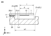
- FIGS. 7 to 9 are schematic partial cross-sectional views of modified examples of the recess 21 in the semiconductor device 100a according to the first embodiment.
- FIGS. 7 to 9 correspond to FIG. 6.
- the semiconductor device 100a shown in FIGS. 7 to 9 basically has the same configuration as the semiconductor device 100a shown in FIGS. 1 to 6 and can achieve the same effects, but the shape of the recess 21 is different.
- the bottom surface 21s1 may extend to the side surface 20s3 of the mounting substrate 2.
- the width w1 of the recess 21 is the distance in the x direction from the side surface 21s2 of the recess 21 to the side surface 20s3 of the mounting substrate 2.
- the lead frames of the first wiring circuit 6a, the second wiring circuit 6b, etc. may be connected to the bottom surface 21s1 of the recess 21.
- the surface morphology of the main surfaces 20s1 of the first wiring circuit side surface 20as2 and the second wiring circuit side surface 20bs2, etc. is superior to that of the bottom surface 21s1 of the recess 21.
- the lead frames of the first wiring circuit 6a, the second wiring circuit 6b, etc. are connected to the main surfaces 20s1 of the first wiring circuit side surface 20as2 and the second wiring circuit side surface 20bs2, etc.
- the side surface 21s2 may have a curved portion R.
- the side surface 21s2 may be a surface that combines a straight portion L and a curved portion R.
- the shape of the inner side surface 21s2 and the outer side surface 21s2 may be different from each other.
- the cross-sectional shape of the inner side surface 21s2 may be a curved shape such as an arc or an ellipse
- the cross-sectional shape of the outer side surface 21s2 may be a straight line.
- the outer side surface 21s2 may be tapered and inclined with respect to the bottom surface 21s1.
- the inner side surface 21s2 may have a curved portion R
- the outer side surface 21s2 may have a straight portion L.
- the shape of the recess 21 in the cross section in the z direction may be a shape that narrows from the opening 21a toward the bottom surface 21s1.
- the recess 21 as described above is preferably filled with an insulating material such as silicone gel or epoxy resin.
- the insulating material filled in the recess 21 may be, for example, sealing resin 7 as shown in FIG. 1.
- the recess 21 may be formed by any method, such as mechanical processing or chemical processing.
- mechanical processing include removal processes such as cutting, grinding, and milling, and molding processes such as pressing, casting, and forging.
- chemical processing include etching.
- a step (S1a) of preparing a semiconductor substrate 1 and a conductive portion 20 is performed.
- a recess 21 is formed on the surface of the conductive portion 20.
- the conductive portion 20 includes a first conductive portion 20a and a second conductive portion 20b. The first conductive portion 20a and the second conductive portion 20b are disposed spaced apart from each other.
- Figure 10 is a schematic plan view showing the conductive portion 20 in the semiconductor device 100a according to the first embodiment.
- Figure 11 is a schematic cross-sectional view taken along line XI-XI in Figure 10.
- the insulating section 3 has an adhesive function for connecting the first conductive section 20a and the second conductive section 20b, and an electrical insulating function for insulating the first conductive section 20a and the second conductive section 20b.
- the material constituting the insulating section 3 is, for example, a thermosetting resin such as epoxy resin.
- a step (S2a) is performed in which the semiconductor substrate 1 is mounted on the conductive portion 20. Specifically, the electrode 11 formed on the first surface 1s1 of the semiconductor substrate 1 is connected to the conductive portion 20 via the joint 5.
- the step (S3a) of connecting the lead frames is carried out.
- the first wiring circuit 6a is connected to the first conductive portion 20a via the joint 5.
- the second wiring circuit 6b is connected to the second conductive portion 20b via the joint 5.
- the third wiring circuit 6c is connected to the upper electrode 11u of the semiconductor substrate 1 via the joint 5.
- the step (S4a) of forming the sealing resin 7 is carried out. Specifically, the support layer 40, the thermally conductive insulating layer 30, and the conductive portion 20 carrying the semiconductor substrate 1 described above are arranged in a metal mold for transfer molding. After that, the sealing resin 7 is formed by transfer molding.
- a semiconductor device 100a includes a semiconductor substrate 1 and a mounting substrate 2.
- the semiconductor substrate 1 has a first surface 1s1.
- the mounting substrate 2 has a main surface 20s1.
- the main surface 20s1 faces the first surface 1s1.
- An electric field intensity mitigating portion 12 and an electrode 11 are formed on the first surface 1s1.
- the electrode 11 is connected to the mounting substrate 2.
- a recess 21 is formed on the main surface 20s1.
- the recess 21 is disposed at a position overlapping the electric field intensity mitigating portion 12 in a plan view of the first surface 1s1.
- the recess 21 can be formed to sufficiently increase the distance between the electric field strength mitigation section 12 and the mounting substrate 2. This reduces the influence of the mounting substrate 2 on the electric field strength mitigation section 12. As a result, the voltage resistance of the semiconductor device 100a is improved.
- FIG. 12 is a schematic bottom view of the semiconductor substrate 1 in the first modified example of the semiconductor device according to the first embodiment.
- FIG. 12 corresponds to FIG. 2.
- FIG. 13 is a schematic plan view of the mounting substrate 2 in the first modified example of the semiconductor device 100a according to the first embodiment.
- FIG. 13 corresponds to FIG. 3.
- the semiconductor device 100a shown in FIG. 12 and FIG. 13 basically has the same configuration as the semiconductor device 100a shown in FIG. 1 to FIG. 6 and can obtain the same effect, but is different in that the third electrode 11c is formed on the first surface 1s1 of the semiconductor substrate 1 as shown in FIG. 12.
- at least one or more third electrodes 11c may be formed on the first surface 1s1.
- the number of the third electrodes 11c may be one or more.
- the third electrode 11c is disposed on the first surface 1s1 at a distance from the first electrode 11a and the second electrode 11b.
- the conductive portion 20 includes a third conductive portion 20c that can be wired in parallel to the second electrode 11b, which is the control electrode.
- the third conductive portion 20c is disposed at a distance from the first conductive portion 20a and the second conductive portion 20b.
- the first conductive portion 20a, the second conductive portion 20b, and the third conductive portion 20c only need to be insulated from one another. It is preferable that the spaces between the first conductive portion 20a, the second conductive portion 20b, and the third conductive portion 20c are filled with an insulating material such as silicone gel or epoxy resin.
- the insulating material filled between the first conductive portion 20a, the second conductive portion 20b, and the third conductive portion 20c may be, for example, the sealing resin 7 shown in FIG. 1.
- either the current sense line or the temperature sense line which is the wiring from the on-chip diode, may be connected to the third conductive portion 20c.
- the third electrode 11c has the same potential as the first electrode 11a.
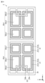
- Fig. 14 is a schematic bottom view of the mounting substrate 2 in the modified example 2 of the semiconductor device 100a according to the first embodiment.
- Fig. 14 corresponds to Fig. 3.
- the mounting substrate 2 shown in Fig. 14 basically has the same configuration as the mounting substrate 2 in the semiconductor device 100a shown in Figs. 1 to 6, and can obtain the same effects, but is different in that the semiconductor device 100a according to the first embodiment has a plurality of semiconductor substrates 1, as shown in Fig. 14.
- the semiconductor device 100a shown in Figures 1 to 6 has one semiconductor substrate 1, but the semiconductor device 100a may have multiple semiconductor substrates 1.
- the semiconductor device 100a may have multiple semiconductor substrates 1 that are different from each other, or multiple semiconductor substrates 1 that have different structures from each other.
- the type of semiconductor substrate 1 has a structure called vertical type, there are no particular restrictions on the number of parallel substrates and combinations.
- the circuit configuration of the semiconductor device 100a is a so-called 2-in-1 type in which two semiconductor substrates 1 are mounted on one module.
- FIG. 14 shows a mounting substrate 2 that configures a half bridge. As shown in FIG. 14, the four first electrode side surfaces 20as1 arranged on both the left and right ends of the mounting substrate 2 may be connected to the semiconductor substrate 1 for the transistor. The four first electrode side surfaces 20as1 arranged in the center of the mounting substrate 2 may be connected to the semiconductor substrate 1 for the transistor.
- FIG. 15 is a schematic cross-sectional view of a semiconductor device 100b according to a second embodiment.
- FIG. 15 corresponds to FIG. 1.
- FIG. 16 is a schematic plan view of a mounting substrate 2 in the semiconductor device 100b according to the second embodiment.
- FIG. 16 corresponds to FIG. 3.
- FIG. 17 is a schematic cross-sectional view taken along line XVII-XVII in FIG. 16.
- FIG. 17 corresponds to FIG. 4.
- the semiconductor device 100b shown in FIGS. 15 to 17 basically has the same configuration as the semiconductor device 100a shown in FIGS. 1 and 6 and can achieve the same effects, but is different in that the member connected to the rear surface 20s2 of the conductive portion 20 is an insulating substrate 31, not a thermally conductive insulating layer 30.
- the mounting substrate 2 has a conductive portion 20, an insulating substrate 31, and a lower electrode 41.
- the insulating substrate 31 is connected to the rear surface 20s2 of the conductive portion 20.
- the lower electrode 41 is connected to the surface of the insulating substrate 31 opposite to the surface to which the conductive portion 20 is connected.
- the surface of the lower electrode 41 opposite to the surface to which the insulating substrate 31 is connected is exposed from the sealing resin 7.
- the material constituting the insulating substrate 31 may be any material, for example, a ceramic whose main component is either Si-N or Al-N.
- the insulating substrate 31 insulates the conductive portion 20 and the lower electrode 41.
- the lower electrode 41 has high thermal conductivity.
- the linear expansion coefficient of the lower electrode 41 is the same as the linear expansion coefficient of the conductive portion 20.
- the material constituting the lower electrode 41 is the same as the material constituting the conductive portion 20.
- the material constituting the lower electrode may include, for example, any one of aluminum (Al), an aluminum alloy, copper (Cu), and a copper alloy.
- the conductive portion 20, insulating substrate 31, and lower electrode 41 may each be joined by a direct joining method or an active metal brazing method.
- the direct joining method is a method in which two constituent materials are joined by a direct reaction.
- the active metal brazing method is a method in which two constituent materials are joined by a brazing material to which an active metal such as titanium or zirconium is added.
- the conductive portion 20, insulating substrate 31, and lower electrode 41 are integrated into the mounting substrate 2, which improves the handleability of the conductive portion 20 during the manufacturing process of the semiconductor device 100b.
- the mounting substrate 2 has an insulating substrate 31 and a lower electrode 41.
- the insulating substrate 31 is connected to the conductive portion 20.
- the lower electrode 41 is connected to the insulating substrate 31.
- the lower electrode 41 is disposed on the side of the insulating substrate 31 opposite to the side on which the conductive portion 20 is disposed.
- the conductive portion 20, the insulating substrate 31, and the lower electrode 41 are integrated into the mounting substrate 2.
- the handleability of the conductive portion 20 during the manufacturing process of the semiconductor device 100b is improved.
- Fig. 18 is a schematic cross-sectional view of a semiconductor device 100c according to a third embodiment.
- Fig. 18 corresponds to Fig. 1.
- the semiconductor device 100c shown in Fig. 18 basically has the same configuration as the semiconductor device 100a shown in Figs. 1 and 6, and can obtain the same effects, but is different in that a sealing resin 7 is formed by a case mold.
- a sealing resin 7 is formed by a case mold.
- a potting resin is used as the sealing resin 7.
- the material constituting the potting resin is, for example, a silicone gel.
- the case 8 is disposed on the support layer 40.
- the case 8 is disposed so as to surround the semiconductor substrate 1.
- the case 8 is fixed to the support layer 40 by adhesive or the like.
- the case 8 and the support layer 40 fixed by adhesive or the like are sealed.
- the material that constitutes the case 8 is preferably, for example, a material that can be injection molded and has high heat resistance and insulating properties. Any material may be used as the material that constitutes the case 8, but it may be, for example, an engineering plastic such as polyphenylene sulfide (PPS).
- PPS polyphenylene sulfide
- a step (S1c) of preparing a semiconductor substrate 1 and a mounting substrate 2 is performed.
- the mounting substrate 2 has a conductive portion 20, a thermally conductive insulating layer 30, and a support layer 40.
- a recess 21 is formed on the surface of the conductive portion 20.
- a step (S2c) is performed in which the semiconductor substrate 1 is mounted on the conductive portion 20. Specifically, the electrode 11 formed on the first surface 1s1 of the semiconductor substrate 1 is connected to the conductive portion 20 via the joint 5.
- the step (S3c) of connecting the lead frames is carried out.
- the first wiring circuit 6a is connected to the first conductive portion 20a via the joint 5.
- the second wiring circuit 6b is connected to the second conductive portion 20b via the joint 5.
- the third wiring circuit 6c is connected to the upper electrode 11u of the semiconductor substrate 1 via the joint 5.
- case 8 is fixed to support layer 40 with adhesive or the like. Then, case 8 is filled with potting resin or the like.
- a lid (not shown) may be mounted on the semiconductor device 100c.
- terminal processing such as bending may be performed on the wiring circuit extending outside the sealing resin 7.
- the semiconductor device 100c according to the third embodiment shown in FIG. 18 can be obtained.
- the semiconductor device 100c further includes a case 8.
- the case 8 surrounds the sealing resin 7.
- Fig. 19 is a schematic cross-sectional view of a semiconductor device 100d according to embodiment 4.
- Fig. 19 corresponds to Fig. 1.
- the semiconductor device 100d shown in Fig. 19 basically has a similar configuration to the semiconductor device 100a shown in Fig. 1 to Fig. 6 and can obtain similar effects, but differs in that it includes a cooler 9.
- the cooler 9 is connected to the back surface of the support layer 40 exposed from the sealing resin 7 via the sixth joint 5f.
- a flow path is formed inside the cooler 9 for circulating a liquid as a refrigerant.
- the cooler 9 in the semiconductor device 100d according to the fourth embodiment is a cooler 9 for liquid cooling, but may also be a cooler 9 for air cooling. In this way, the heat dissipation properties of the semiconductor device 100d are improved.
- the sixth joint 5f can be made of solder, but it is particularly preferable to use a material that has high thermal conductivity and can ensure long-term reliability even when the joint is thin.
- the material constituting the cooler 9 may be any material having high thermal conductivity.
- the material constituting the cooler 9 may include, for example, aluminum (Al), an aluminum alloy, copper (Cu), or a copper alloy.
- the sealing resin 7 when the sealing resin 7 is formed by case molding, it is preferable to fill the case 8 with potting resin after bonding the cooler 9 to the mounting substrate 2.
- the semiconductor device 100d further includes a cooler 9.
- the cooler 9 is connected to the mounting board 2.
- Fig. 20 is a schematic cross-sectional view of a semiconductor device 100e according to embodiment 5.
- Fig. 20 corresponds to Fig. 1.
- the semiconductor device 100e shown in Fig. 20 basically has the same configuration as the semiconductor device 100a shown in Fig. 1 to Fig. 6 and can obtain the same effects, but differs in that the sealing resin 7 seals a part of the cooler 9.
- the cooler 9 plays the role of the support layer 40 of the mounting substrate 2. Therefore, the thermally conductive insulating layer 30 is connected to the cooler 9. Therefore, the cooler 9 does not have to be connected to the thermally conductive insulating layer 30 via the sixth joint 5f shown in FIG. 19. In this way, the heat dissipation properties of the semiconductor device 100e are further improved.
- FIG. 21 is a schematic cross-sectional view of a modified example of the semiconductor device 100e according to the fifth embodiment.
- FIG. 21 corresponds to FIG. 1.
- the semiconductor device 100e shown in FIG. 21 basically has the same configuration as the semiconductor device 100e shown in FIG. 20 and can achieve the same effects, but differs in that the sealing resin 7 seals the entire cooler 9.
- the semiconductor device 100e has at least a part of the cooler 9 sealed therein.
Landscapes
- Structures Or Materials For Encapsulating Or Coating Semiconductor Devices Or Solid State Devices (AREA)
Abstract
Un dispositif à semi-conducteur (100a) comprend un substrat semi-conducteur (1) et un substrat de montage (2). Le substrat semi-conducteur (1) a une première surface (1s1). Le substrat de montage (2) a une surface principale (20s1). La surface principale (20s1) fait face à la première surface (1s1). Une partie de relaxation de l'intensité de champ électrique (12) et une électrode (11) sont formées sur la première surface (1s1). L'électrode (11) est connectée au substrat de montage (2). Un évidement (21) est formé dans la surface principale (20s1). L'évidement (21) est disposé à une position chevauchant la partie de relaxation de l'intensité de champ électrique (12) dans une vue en plan de la première surface (1s1).
Priority Applications (3)
| Application Number | Priority Date | Filing Date | Title |
|---|---|---|---|
| PCT/JP2023/034522 WO2025062637A1 (fr) | 2023-09-22 | 2023-09-22 | Dispositif à semi-conducteur |
| CN202380102351.0A CN121890330A (zh) | 2023-09-22 | 2023-09-22 | 半导体装置 |
| JP2024517145A JP7678934B1 (ja) | 2023-09-22 | 2023-09-22 | 半導体装置 |
Applications Claiming Priority (1)
| Application Number | Priority Date | Filing Date | Title |
|---|---|---|---|
| PCT/JP2023/034522 WO2025062637A1 (fr) | 2023-09-22 | 2023-09-22 | Dispositif à semi-conducteur |
Publications (1)
| Publication Number | Publication Date |
|---|---|
| WO2025062637A1 true WO2025062637A1 (fr) | 2025-03-27 |
Family
ID=95072624
Family Applications (1)
| Application Number | Title | Priority Date | Filing Date |
|---|---|---|---|
| PCT/JP2023/034522 Pending WO2025062637A1 (fr) | 2023-09-22 | 2023-09-22 | Dispositif à semi-conducteur |
Country Status (3)
| Country | Link |
|---|---|
| JP (1) | JP7678934B1 (fr) |
| CN (1) | CN121890330A (fr) |
| WO (1) | WO2025062637A1 (fr) |
Citations (2)
| Publication number | Priority date | Publication date | Assignee | Title |
|---|---|---|---|---|
| JPH04167565A (ja) * | 1990-10-31 | 1992-06-15 | Fujitsu Ltd | フリップチップ型受光素子 |
| JP2000114413A (ja) * | 1998-09-29 | 2000-04-21 | Sony Corp | 半導体装置、その製造方法および部品の実装方法 |
Family Cites Families (8)
| Publication number | Priority date | Publication date | Assignee | Title |
|---|---|---|---|---|
| JP3639515B2 (ja) * | 2000-09-04 | 2005-04-20 | 三洋電機株式会社 | Mosfetの実装構造の製造方法 |
| US7786558B2 (en) * | 2005-10-20 | 2010-08-31 | Infineon Technologies Ag | Semiconductor component and methods to produce a semiconductor component |
| ITMI20111213A1 (it) * | 2011-06-30 | 2012-12-31 | St Microelectronics Srl | Dispositivo elettronico a semi-ponte con dissipatore di calore ausiliario comune |
| US9673163B2 (en) * | 2011-10-18 | 2017-06-06 | Rohm Co., Ltd. | Semiconductor device with flip chip structure and fabrication method of the semiconductor device |
| US9653386B2 (en) * | 2014-10-16 | 2017-05-16 | Infineon Technologies Americas Corp. | Compact multi-die power semiconductor package |
| EP3648159B1 (fr) * | 2018-10-31 | 2021-12-15 | Infineon Technologies Austria AG | Boîtier à semi-conducteurs et procédé de fabrication d'un boîtier à semi-conducteurs |
| WO2021112590A2 (fr) * | 2019-12-05 | 2021-06-10 | 주식회사 아모센스 | Module semi-conducteur de puissance |
| IT202000032267A1 (it) * | 2020-12-23 | 2022-06-23 | St Microelectronics Srl | Dispositivo elettronico incapsulato ad elevata dissipazione termica e relativo procedimento di fabbricazione |
-
2023
- 2023-09-22 CN CN202380102351.0A patent/CN121890330A/zh active Pending
- 2023-09-22 WO PCT/JP2023/034522 patent/WO2025062637A1/fr active Pending
- 2023-09-22 JP JP2024517145A patent/JP7678934B1/ja active Active
Patent Citations (2)
| Publication number | Priority date | Publication date | Assignee | Title |
|---|---|---|---|---|
| JPH04167565A (ja) * | 1990-10-31 | 1992-06-15 | Fujitsu Ltd | フリップチップ型受光素子 |
| JP2000114413A (ja) * | 1998-09-29 | 2000-04-21 | Sony Corp | 半導体装置、その製造方法および部品の実装方法 |
Also Published As
| Publication number | Publication date |
|---|---|
| CN121890330A (zh) | 2026-04-17 |
| JP7678934B1 (ja) | 2025-05-16 |
| JPWO2025062637A1 (fr) | 2025-03-27 |
Similar Documents
| Publication | Publication Date | Title |
|---|---|---|
| JP3910383B2 (ja) | パワーモジュールおよびインバータ | |
| US7816784B2 (en) | Power quad flat no-lead semiconductor die packages with isolated heat sink for high-voltage, high-power applications, systems using the same, and methods of making the same | |
| CN104285294B (zh) | 半导体装置及该半导体装置的制造方法 | |
| TWI855173B (zh) | 半導體裝置 | |
| US9704819B1 (en) | Three dimensional fully molded power electronics module having a plurality of spacers for high power applications | |
| US8198712B2 (en) | Hermetically sealed semiconductor device module | |
| JP5017332B2 (ja) | インバータ | |
| JP2004296588A (ja) | 半導体装置 | |
| US10903138B2 (en) | Semiconductor device and method of manufacturing the same | |
| WO2021210402A1 (fr) | Dispositif à semi-conducteurs | |
| CN110771027B (zh) | 功率半导体装置及使用该装置的电力转换装置 | |
| CN111354710A (zh) | 半导体装置及其制造方法 | |
| JP2012209470A (ja) | 半導体装置、半導体装置モジュール及び半導体装置の製造方法 | |
| JP7018756B2 (ja) | パワーモジュール用基板およびパワーモジュール | |
| JP4096741B2 (ja) | 半導体装置 | |
| KR101644913B1 (ko) | 초음파 용접을 이용한 반도체 패키지 및 제조 방법 | |
| JP2009170645A (ja) | 電力変換装置及びその製造方法 | |
| JP5056105B2 (ja) | 半導体装置およびその製造方法 | |
| JP7495225B2 (ja) | 半導体装置 | |
| JP7678934B1 (ja) | 半導体装置 | |
| JP7117960B2 (ja) | パワーモジュール用基板およびパワーモジュール | |
| JP2019009280A (ja) | 半導体装置 | |
| JP4403166B2 (ja) | パワーモジュールおよび電力変換装置 | |
| JP7613169B2 (ja) | 半導体モジュール | |
| US20230096381A1 (en) | Semiconductor device and method for manufacturing semiconductor device |
Legal Events
| Date | Code | Title | Description |
|---|---|---|---|
| ENP | Entry into the national phase |
Ref document number: 2024517145 Country of ref document: JP Kind code of ref document: A |
|
| WWE | Wipo information: entry into national phase |
Ref document number: 2024517145 Country of ref document: JP |
|
| 121 | Ep: the epo has been informed by wipo that ep was designated in this application |
Ref document number: 23953114 Country of ref document: EP Kind code of ref document: A1 |