CN100431103C - High-k dielectric films, methods of forming the same, and related semiconductor devices - Google Patents
High-k dielectric films, methods of forming the same, and related semiconductor devices Download PDFInfo
- Publication number
- CN100431103C CN100431103C CNB038268728A CN03826872A CN100431103C CN 100431103 C CN100431103 C CN 100431103C CN B038268728 A CNB038268728 A CN B038268728A CN 03826872 A CN03826872 A CN 03826872A CN 100431103 C CN100431103 C CN 100431103C
- Authority
- CN
- China
- Prior art keywords
- content
- layer
- nitrogen
- top layer
- metallic silicon
- Prior art date
- Legal status (The legal status is an assumption and is not a legal conclusion. Google has not performed a legal analysis and makes no representation as to the accuracy of the status listed.)
- Expired - Fee Related
Links
Images


Classifications
-
- H—ELECTRICITY
- H10—SEMICONDUCTOR DEVICES; ELECTRIC SOLID-STATE DEVICES NOT OTHERWISE PROVIDED FOR
- H10D—INORGANIC ELECTRIC SEMICONDUCTOR DEVICES
- H10D64/00—Electrodes of devices having potential barriers
- H10D64/01—Manufacture or treatment
- H10D64/013—Manufacture or treatment of electrodes having a conductor capacitively coupled to a semiconductor by an insulator
- H10D64/01302—Manufacture or treatment of electrodes having a conductor capacitively coupled to a semiconductor by an insulator the insulator being formed after the semiconductor body, the semiconductor being silicon
- H10D64/01332—Making the insulator
- H10D64/01336—Making the insulator on single crystalline silicon, e.g. chemical oxidation using a liquid
- H10D64/0134—Making the insulator on single crystalline silicon, e.g. chemical oxidation using a liquid with a treatment, e.g. annealing, after the formation of the insulator and before the formation of the conductor
-
- H—ELECTRICITY
- H10—SEMICONDUCTOR DEVICES; ELECTRIC SOLID-STATE DEVICES NOT OTHERWISE PROVIDED FOR
- H10D—INORGANIC ELECTRIC SEMICONDUCTOR DEVICES
- H10D64/00—Electrodes of devices having potential barriers
- H10D64/01—Manufacture or treatment
- H10D64/013—Manufacture or treatment of electrodes having a conductor capacitively coupled to a semiconductor by an insulator
- H10D64/01302—Manufacture or treatment of electrodes having a conductor capacitively coupled to a semiconductor by an insulator the insulator being formed after the semiconductor body, the semiconductor being silicon
- H10D64/01332—Making the insulator
- H10D64/01336—Making the insulator on single crystalline silicon, e.g. chemical oxidation using a liquid
- H10D64/01344—Making the insulator on single crystalline silicon, e.g. chemical oxidation using a liquid in a nitrogen-containing ambient, e.g. N2O oxidation
-
- H—ELECTRICITY
- H10—SEMICONDUCTOR DEVICES; ELECTRIC SOLID-STATE DEVICES NOT OTHERWISE PROVIDED FOR
- H10D—INORGANIC ELECTRIC SEMICONDUCTOR DEVICES
- H10D64/00—Electrodes of devices having potential barriers
- H10D64/60—Electrodes characterised by their materials
- H10D64/66—Electrodes having a conductor capacitively coupled to a semiconductor by an insulator, e.g. MIS electrodes
- H10D64/68—Electrodes having a conductor capacitively coupled to a semiconductor by an insulator, e.g. MIS electrodes characterised by the insulator, e.g. by the gate insulator
- H10D64/681—Electrodes having a conductor capacitively coupled to a semiconductor by an insulator, e.g. MIS electrodes characterised by the insulator, e.g. by the gate insulator having a compositional variation, e.g. multilayered
- H10D64/685—Electrodes having a conductor capacitively coupled to a semiconductor by an insulator, e.g. MIS electrodes characterised by the insulator, e.g. by the gate insulator having a compositional variation, e.g. multilayered being perpendicular to the channel plane
-
- H—ELECTRICITY
- H10—SEMICONDUCTOR DEVICES; ELECTRIC SOLID-STATE DEVICES NOT OTHERWISE PROVIDED FOR
- H10D—INORGANIC ELECTRIC SEMICONDUCTOR DEVICES
- H10D64/00—Electrodes of devices having potential barriers
- H10D64/60—Electrodes characterised by their materials
- H10D64/66—Electrodes having a conductor capacitively coupled to a semiconductor by an insulator, e.g. MIS electrodes
- H10D64/68—Electrodes having a conductor capacitively coupled to a semiconductor by an insulator, e.g. MIS electrodes characterised by the insulator, e.g. by the gate insulator
- H10D64/693—Electrodes having a conductor capacitively coupled to a semiconductor by an insulator, e.g. MIS electrodes characterised by the insulator, e.g. by the gate insulator the insulator comprising nitrogen, e.g. nitrides, oxynitrides or nitrogen-doped materials
-
- H—ELECTRICITY
- H10—SEMICONDUCTOR DEVICES; ELECTRIC SOLID-STATE DEVICES NOT OTHERWISE PROVIDED FOR
- H10D—INORGANIC ELECTRIC SEMICONDUCTOR DEVICES
- H10D64/00—Electrodes of devices having potential barriers
- H10D64/01—Manufacture or treatment
- H10D64/013—Manufacture or treatment of electrodes having a conductor capacitively coupled to a semiconductor by an insulator
- H10D64/01302—Manufacture or treatment of electrodes having a conductor capacitively coupled to a semiconductor by an insulator the insulator being formed after the semiconductor body, the semiconductor being silicon
- H10D64/01332—Making the insulator
- H10D64/01336—Making the insulator on single crystalline silicon, e.g. chemical oxidation using a liquid
- H10D64/01342—Making the insulator on single crystalline silicon, e.g. chemical oxidation using a liquid by deposition, e.g. evaporation, ALD or laser deposition
-
- Y—GENERAL TAGGING OF NEW TECHNOLOGICAL DEVELOPMENTS; GENERAL TAGGING OF CROSS-SECTIONAL TECHNOLOGIES SPANNING OVER SEVERAL SECTIONS OF THE IPC; TECHNICAL SUBJECTS COVERED BY FORMER USPC CROSS-REFERENCE ART COLLECTIONS [XRACs] AND DIGESTS
- Y10—TECHNICAL SUBJECTS COVERED BY FORMER USPC
- Y10S—TECHNICAL SUBJECTS COVERED BY FORMER USPC CROSS-REFERENCE ART COLLECTIONS [XRACs] AND DIGESTS
- Y10S257/00—Active solid-state devices, e.g. transistors, solid-state diodes
- Y10S257/914—Polysilicon containing oxygen, nitrogen, or carbon, e.g. sipos
Landscapes
- Insulated Gate Type Field-Effect Transistor (AREA)
- Formation Of Insulating Films (AREA)
- Semiconductor Memories (AREA)
Abstract
Description
技术领域 technical field
本发明涉及高k介电膜,及其形成方法和相关的半导体器件,具体涉及与集成电路中用于场效应半导体器件的栅极电介质或沟槽电容器的电容器电介质有关的高k介电膜。The present invention relates to high-k dielectric films, methods of forming the same, and related semiconductor devices, in particular to high-k dielectric films related to gate dielectrics for field-effect semiconductor devices or capacitor dielectrics for trench capacitors in integrated circuits.
背景技术 Background technique
为了形成诸如CMOS器件(互补金属氧化物半导体)、MOSFET器件(金属氧化物半导体场效应晶体管)或高存储器件例如DRAM(动态随机存取存储器)的半导体器件,通常需要在例如硅晶片的衬底上形成薄的、高介电常数(高k)的膜。已经开发了多种技术用以在半导体晶片上形成这种薄膜。In order to form semiconductor devices such as CMOS devices (Complementary Metal Oxide Semiconductors), MOSFET devices (Metal Oxide Semiconductor Field Effect Transistors), or high memory devices such as DRAM (Dynamic Random Access Memory), it is generally necessary to A thin, high dielectric constant (high-k) film is formed on it. Various techniques have been developed to form such thin films on semiconductor wafers.
在过去,栅极介电层使用二氧化硅形成。然而,上述器件的按比例缩小增加了对与二氧化硅相比具有更高的介电常数的栅极电介质的要求。这需要达到超薄氧化物等效厚度(EOT,等效氧化物厚度)而不以栅极漏电流折衷。In the past, the gate dielectric layer was formed using silicon dioxide. However, scaling down of the aforementioned devices has increased the requirement for a gate dielectric with a higher dielectric constant than silicon dioxide. This requires achieving ultra-thin oxide equivalent thickness (EOT, equivalent oxide thickness) without compromising gate leakage.
详细地说,由于半导体器件已经按比例缩小为更小的尺寸,因此有效栅极电介质厚度已经变得更薄。由于直接隧穿的原因,例如SiO2和SiOxNy的常规栅极电介质的持续按比例缩放几乎已经达到很高的栅极漏电流的基本限制,其在低漏电流的按比例缩放的器件要求中是不可接受的。为了抑制高漏电流,几种过渡金属氧化物和硅酸盐的高k膜已经被研究来代替SiO2和SiOxNy,例如HfO2、ZrO2、铪铝酸盐、锆铝酸盐、锆硅酸盐、铪硅酸盐和诸如La2O3、Pr2O3、及Gd2O3之类的镧系氧化物。In detail, as semiconductor devices have been scaled to smaller dimensions, the effective gate dielectric thickness has become thinner. The continued scaling of conventional gate dielectrics such as SiO2 and SiOxNy has almost reached the fundamental limit of very high gate leakage due to direct tunneling, which in scaled devices with low leakage current request is not acceptable. To suppress high leakage currents, high-k films of several transition metal oxides and silicates have been investigated to replace SiO 2 and SiO x N y , such as HfO 2 , ZrO 2 , hafnium aluminate, zirconium aluminate, Zirconium silicates, hafnium silicates , and lanthanide oxides such as La2O3 , Pr2O3 , and Gd2O3 .
然而,这些常规材料已经显示出多个缺点。根据S.OHMT等人的“Rare earth metal oxide gate thin films prepared by E-beamdeposition”,International Workshop on Gate Insulator2001,Tokyo,Japan,得知ZrO2或HfO2已经显示出微晶体形成,结果产生高漏电流。However, these conventional materials have exhibited several disadvantages. According to "Rare earth metal oxide gate thin films prepared by E-beamdeposition" by S. OHMT et al., International Workshop on Gate Insulator 2001, Tokyo, Japan, it is known that ZrO 2 or HfO 2 has shown microcrystal formation, resulting in high leakage current.
此外,从2002年的Tech.Dig.VLS I的第84页的J.H.LEE等人的“Poly-Si gate CMOSFETs with HfO2-Al2O3 laminate gatedielectric for low power applications”中得知HfO2-Al2O3叠层或铪铝酸盐由于高k介电膜内的固定电荷的缘故而具有严重的迁移率退化。Furthermore , it is known that HfO 2 -Al 2 O 3 stacks or hafnium aluminates have severe mobility degradation due to fixed charges within the high-k dielectric film.
而且,TAKESHI,YAMAGUCHI等人的“Additional scatteringeffects for mobility degradation in Hf-silicate gate MISFETs”Tech.Dig.IEDM 2002报道在锆硅酸盐或铪硅酸盐的情况下,HfO2和SiO2区域中的膜通过高温退火的相位分离也引起迁移率退化。Moreover, "Additional scattering effects for mobility degradation in Hf-silicate gate MISFETs" by TAKESHI, YAMAGUCHI et al. Tech.Dig.IEDM 2002 reported that in the case of zirconium silicate or hafnium silicate, the HfO 2 and SiO 2 regions Phase separation of the film by high temperature annealing also causes mobility degradation.
对于镧系氧化物来说,漏电流结果指示出镧系氧化物可能是未来电介质的选择。然而,根据H.IWAI等人的“Advanced gate dielectricmaterials for Sub-100nm CMOS”,Tech.Dig.IEDM 2002,报道,这些镧系氧化物在随后的热退火之后也在Si衬底上形成界面层,其可以表示这些镧系氧化物的热不稳定性。For lanthanide oxides, the leakage current results indicate that lanthanide oxides may be the dielectric of choice in the future. However, according to "Advanced gate dielectric materials for Sub-100nm CMOS" by H.IWAI et al., Tech.Dig.IEDM 2002, it is reported that these lanthanide oxides also form interfacial layers on Si substrates after subsequent thermal annealing, It may be indicative of the thermal instability of these lanthanide oxides.
而且,从例如栅极层到Si衬底的诸如硼渗透的杂质渗透是通过这些高k介电膜来解决的另一问题。即使已知在HfSixOy上结合氮用来抑制这种例如硼渗透,并改善热稳定性,但是还报道了需要HfSixOyNz中超过80%的Si/[Si+Hf]比例的高Si含量来防止平带电压移动,结果严重降低了膜的介电常数,即使是在30原子百分比的高氮含量的情况下(参见M.KOYAMA等人的“Effects of nitrogen inHfSiON gate dielectric on the electrical and thermalcharacteristics”,Tech.Dig.IEDM 2002,34-1)。该很高S i含量HfSixOyNz的低k介电膜就介电常数来说与常规SiOxNy几乎相同,并且考虑到代替SiOxNy则不再是有意义的。Si衬底上的相应膜形成的其它技术问题在于,在介电层和Si衬底之间的界面处的高氮浓度可被随后的高热退火引发而使迁移率退化。Also, impurity penetration such as boron penetration from eg the gate layer to the Si substrate is another problem addressed by these high-k dielectric films. Even though incorporation of nitrogen on HfSixOy is known to suppress such e.g. boron permeation, and improve thermal stability, it has also been reported that a Si /[Si+Hf] ratio of more than 80% in HfSixOyNz is required The high Si content of Si to prevent the shift of the flat-band voltage results in a severe decrease in the dielectric constant of the film, even at a high nitrogen content of 30 atomic percent (see "Effects of nitrogen in HfSiON gate dielectric on M. KOYAMA et al. the electrical and thermal characteristics", Tech. Dig. IEDM 2002, 34-1). The low-k dielectric film of the very high Si content HfSixOyNz is almost the same as conventional SiOxNy in terms of dielectric constant, and it no longer makes sense to consider replacing SiOxNy . A further technical problem with the corresponding film formation on Si substrates is that the high nitrogen concentration at the interface between the dielectric layer and the Si substrate can be induced by subsequent high thermal annealing to degrade the mobility.
因此,需要提供改善的高k介电膜,及其形成方法和相关的半导体器件。Accordingly, there is a need to provide improved high-k dielectric films, methods of forming the same, and related semiconductor devices.
发明内容 Contents of the invention
根据本发明,形成在衬底上的半导体器件的高k介电膜至少包括具有第一氮含量和第一硅含量的金属硅氮氧化物的底层,和具有第二氮含量和第二硅含量的金属硅氮氧化物的顶层,其中顶层的所述第二氮含量高于底层的所述第一氮含量,并且顶层的所述第二硅含量高于底层的所述第一硅含量。According to the present invention, a high-k dielectric film of a semiconductor device formed on a substrate includes at least an underlayer of metal silicon oxynitride having a first nitrogen content and a first silicon content, and having a second nitrogen content and a second silicon content A top layer of metal silicon oxynitride, wherein said second nitrogen content of the top layer is higher than said first nitrogen content of the bottom layer, and said second silicon content of the top layer is higher than said first silicon content of the bottom layer.
根据一个实施例,高k介电膜构成多层堆叠,其包括形成在所述底层和所述顶层之间的金属硅氮氧化物的至少一个中间层,其具有另一氮含量和另一硅含量,其中相应的另一氮和硅含量在所述相应的第一和第二氮和硅含量之间。According to one embodiment, the high-k dielectric film constitutes a multilayer stack comprising at least one intermediate layer of metal silicon oxynitride formed between said bottom layer and said top layer, having another nitrogen content and another silicon content, wherein the respective another nitrogen and silicon content is between said respective first and second nitrogen and silicon contents.
根据本发明的优选实施例,顶层厚度等于或低于高k介电膜中的剩余层的厚度的总和。According to a preferred embodiment of the present invention, the thickness of the top layer is equal to or lower than the sum of the thicknesses of the remaining layers in the high-k dielectric film.
形成高k介电膜的方法包括以下步骤,即在衬底上形成具有第一氮含量和第一硅含量的金属硅氮氧化物的底层,以及形成具有第二氮含量和第二硅含量的金属硅氮氧化物的顶层,其中所述第二氮含量高于所述第一氮含量,并且所述第二硅含量高于相应层的所述第一硅含量。The method of forming a high-k dielectric film includes the steps of forming an underlayer of metal silicon oxynitride having a first nitrogen content and a first silicon content on a substrate, and forming a metal silicon oxynitride layer having a second nitrogen content and a second silicon content. A top layer of metal silicon oxynitride, wherein said second nitrogen content is higher than said first nitrogen content, and said second silicon content is higher than said first silicon content of a corresponding layer.
为了进一步改善迁移率,尤其是当在场效应晶体管中用作栅极电介质时,该方法进一步包括在形成底层之前在衬底上形成氧化硅的衬底界面层的步骤。To further improve mobility, especially when used as a gate dielectric in field effect transistors, the method further includes the step of forming a substrate interface layer of silicon oxide on the substrate before forming the bottom layer.
另外,具有另一氮含量和另一硅含量的金属硅氮氧化物的至少一个中间层形成在底层上,其中相应的另一氮含量和另一硅含量高于前面层的所述氮含量和硅含量。In addition, at least one intermediate layer of metal silicon oxynitride having another nitrogen content and another silicon content is formed on the bottom layer, wherein the corresponding another nitrogen content and another silicon content are higher than said nitrogen content and another silicon content of the preceding layer. Silicon content.
在替换实施例中,形成高k介电膜的方法包括以下步骤,即在衬底上形成具有第一硅含量的金属硅氧化物的预底层,形成具有第二硅含量的金属硅氧化物的预顶层,其中第二硅含量高于第一硅含量,并且执行N2等离子体处理以将所述预底层转变成具有第一氮含量的金属硅氮氧化物底层,并将所述预顶层转变成具有第二氮含量的金属硅氮氧化物顶层,其中所述第二氮含量高于所述第一氮含量。In an alternative embodiment, a method of forming a high-k dielectric film includes the steps of forming a pre-underlayer of a metal silicon oxide having a first silicon content on a substrate, forming a metal silicon oxide having a second silicon content a pre-top layer, wherein a second silicon content is higher than the first silicon content, and a N2 plasma treatment is performed to transform the pre-bottom layer into a metal silicon oxynitride bottom layer having the first nitrogen content, and to transform the pre-top layer forming a metal silicon oxynitride top layer having a second nitrogen content, wherein the second nitrogen content is higher than the first nitrogen content.
并且,在该替换实施例中,具有另一硅含量的金属硅氧化物的至少一个中间层形成,其中相应的另一硅含量高于前面层的硅含量,并且其中在N2等离子体处理期间,至少一个中间层被转变成具有另一氮含量的至少一个金属硅氮氧化物中间层,其中相应的另一氮含量高于前面层的氮含量。Also, in this alternative embodiment, at least one intermediate layer of metal silicon oxide having another silicon content is formed, wherein the corresponding other silicon content is higher than that of the previous layer, and wherein during the N2 plasma treatment , at least one intermediate layer is transformed into at least one metal silicon oxynitride intermediate layer having another nitrogen content, wherein the corresponding further nitrogen content is higher than the nitrogen content of the preceding layer.
附图说明Description of drawings
根据以下详细描述并参考附图,本发明的目的和优点将变得明显,其中:Objects and advantages of the present invention will become apparent from the following detailed description, taken with reference to the accompanying drawings, in which:
图1A和1B是示出用于制作根据第一实施例的高k介电膜的基本步骤的部分截面图;1A and 1B are partial cross-sectional views showing basic steps for fabricating a high-k dielectric film according to a first embodiment;
图2是根据第二实施例的高k介电膜的部分截面图;2 is a partial cross-sectional view of a high-k dielectric film according to a second embodiment;
图3A~3D是示出用于制作根据第三实施例的高k介电膜的基本步骤的部分截面图;3A to 3D are partial cross-sectional views showing basic steps for fabricating a high-k dielectric film according to a third embodiment;
图4是使用高k介电膜的场效应半导体器件的部分截面图;以及4 is a partial cross-sectional view of a field effect semiconductor device using a high-k dielectric film; and
图5是使用高k介电膜的沟槽电容器的部分截面图。5 is a partial cross-sectional view of a trench capacitor using a high-k dielectric film.
具体实施方式 Detailed ways
虽然本发明可允许各种修改和替换形式,但是其具体实施例在附图中借助实例被示出,并在此被详细描述。然而,应当理解,该处的附图和详细描述并不旨在将本发明限制在所公开的具体形式。相反,本发明将覆盖落入本发明的精神和范围内的所有修改、等价物和替换While the invention is susceptible to various modifications and alternative forms, specific embodiments thereof are shown by way of example in the drawings and described in detail herein. It should be understood, however, that the drawings and detailed description herein are not intended to limit the invention to the precise form disclosed. On the contrary, the invention is to cover all modifications, equivalents, and alternatives falling within the spirit and scope of the invention
图1A和1B示出说明用于产生根据本发明的第一实施例的高k介电膜的基本步骤的局部截面图。1A and 1B show partial cross-sectional views illustrating basic steps for producing a high-k dielectric film according to a first embodiment of the present invention.
根据图1A,单晶Si衬底1用作半导体衬底,在其表面上借助层淀积法形成金属硅氮氧化物(MSixBOyBNzB)的底层B。According to FIG. 1A, a single
根据图1B,在底层B的表面上,由相同的金属硅氮氧化物形成顶层T,然而,具有不同的硅含量和氮含量。详细地说,淀积的顶层T构成具有第二氮含量zT和第二硅含量xT的MSixTOyTNzT。底层和顶层B和T的第一和第二氮含量以及第一和第二硅含量xB和xT以这种方式来选择,即顶层T的第二氮含量zT高于底层的第一氮含量zB,并且顶层T的第二硅含量xT高于底层的第一硅含量xB。According to FIG. 1B , on the surface of the bottom layer B, the top layer T is formed from the same metallic silicon oxynitride, however, with different silicon and nitrogen contents. In detail, the deposited top layer T constitutes MSi xTO yT N zT with a second nitrogen content zT and a second silicon content xT. The first and second nitrogen content and the first and second silicon content xB and xT of the bottom and top layers B and T are selected in such a way that the second nitrogen content zT of the top layer T is higher than the first nitrogen content zB of the bottom layer , and the second silicon content xT of the top layer T is higher than the first silicon content xB of the bottom layer.
MSixOyNz层中的下标x、y和z或xB、yB和zB或xT、yT和zT是表示分子中的原子百分比的正实数。相应层中的氮原子百分比通过(z/(1+x+y+z))×100来计算。通常,Si和M(金属)浓度分别用(x/(1+x))×100和(1/(1+x))×100来表示。The subscripts x , y and z or xB, yB and zB or xT, yT and zT in the layer of MSixOyNz are positive real numbers denoting the atomic percentage in the molecule. The atomic percentage of nitrogen in the corresponding layer was calculated by (z/(1+x+y+z))×100. Usually, Si and M (metal) concentrations are represented by (x/(1+x))×100 and (1/(1+x))×100, respectively.
由此,根据图1B所示的双层堆叠构成了具有改善特性的新的高k介电膜2。详细地说,该双层堆叠的高氮含量顶层T对有效防止例如硼从掺硼的多晶硅电极(未示出)扩散到场效应器件沟道中起关键作用,而低氮含量底层B有助于防止该沟道和/或衬底1内的迁移率退化。而且,由于金属硅氮氧化物中的Si含量的降低与金属含量的增加有关,而根据第一实施例的双层堆叠的介电常数的增加提供了比类似的高Si含量金属硅氮氧化物的现有技术更高的介电常数。因此,有可能进一步按比例缩小有效的氧化物厚度(EOT),同时防止尤其由直接隧穿引起的泄漏。Thus, a new high-k
根据本发明,顶层T中的Si和N浓度需要高于底层B中的,例如xT>xB,zT>zB。相对于底层B的顶层T中的N和Si的比例进一步取决于考虑什么金属硅氧化物。在金属硅氮氧化物层中的金属M是Hf的情况下,其是HfSixOyNz,HfSixOyNz的Si/(Hf+Si)比例需要在70%~95%的范围内,并且N浓度与30原子百分比一样高。由此,对于使用Hf作为金属的顶层T中的固定Si和N浓度来说,底层B的N和Si含量需要低于顶层T的,并且N原子百分比在15%~25%的范围内,以及Si/(Hf+Si)比例在20%~60%的范围内。According to the present invention, the concentration of Si and N in the top layer T needs to be higher than that in the bottom layer B, eg xT>xB, zT>zB. The ratio of N and Si in the top layer T relative to the bottom layer B further depends on what metal silicon oxide is considered. In the case where the metal M in the metal silicon oxynitride layer is Hf , which is HfSixOyNz , the Si/(Hf + Si) ratio of HfSixOyNz needs to be in the range of 70 % to 95% within, and the N concentration is as high as 30 atomic percent. Thus, for a fixed Si and N concentration in the top layer T using Hf as metal, the N and Si content of the bottom layer B needs to be lower than that of the top layer T, and the N atomic percentage is in the range of 15% to 25%, and The ratio of Si/(Hf+Si) is in the range of 20% to 60%.
关于不同层的厚度,应当注意顶层T应当具有比高k介电膜2内的其它层之和的厚度更低的厚度,或者相等。即,根据第一实施例的双层结构的顶层T应当薄于或等于底层B。Regarding the thicknesses of the different layers, it should be noted that the top layer T should have a lower thickness than the sum of the thicknesses of the other layers within the high-
在形成高k介电膜2之后,退火工艺(在N2或其它气体中,在超过600℃的温度下)有助于使层堆叠密度增加并减少缺陷,以改善高k介电膜2的质量(尤其改善漏电流特性)。After forming the high-
图2示出了根据第二实施例的高k介电膜的部分截面图,其中相同的参考数字指的是相同或相应的层,并省略了这些层的重复描述。2 shows a partial cross-sectional view of a high-k dielectric film according to a second embodiment, wherein the same reference numerals refer to the same or corresponding layers, and repeated descriptions of these layers are omitted.
根据第二实施例,衬底界面层I形成在衬底1的表面上,而高k介电膜2的相应的另外的层形成在该衬底界面层I的表面上。在Si衬底1的情况下,该衬底界面层优选构成氧化硅,其进一步增加了衬底内的迁移率,并减少了衬底1表面处的缺陷。According to the second embodiment, a substrate interface layer I is formed on the surface of a
除了所示的根据第一和第二实施例的具有金属硅氮氧化物底层和顶层的双层MSixOyNz堆叠之外,至少另外的金属硅氮氧化物的金属层也可形成在所述底层B和所述顶层T之间,具有另一氮含量和另一硅含量,其中相应的另一氮含量和另一硅含量在底层B和顶层T的所述第一和第二氮和硅含量之间。具体地说,分别形成的中间层的另一氮含量和另一硅含量高于在前面步骤中形成的金属硅氮氧化物的相应的氮和硅含量。In addition to the shown double-layer MSixOyNz stacks with metal silicon oxynitride bottom and top layers according to the first and second embodiments, at least additional metal layers of metal silicon oxynitride can also be formed on Between said bottom layer B and said top layer T, there is another nitrogen content and another silicon content, wherein the corresponding another nitrogen content and another silicon content are in said first and second nitrogen content of bottom B and top layer T and silicon content. Specifically, another nitrogen content and another silicon content of the respectively formed intermediate layers are higher than the corresponding nitrogen and silicon contents of the metal silicon oxynitride formed in the preceding steps.
顶层T的厚度也等于或低于高k介电膜或多层堆叠中剩余层的厚度总和,即底层和另外的中间层。The thickness of the top layer T is also equal to or lower than the sum of the thicknesses of the remaining layers in the high-k dielectric film or multilayer stack, ie, the bottom layer and additional intermediate layers.
关于形成上述金属硅氮氧化物层的优选方法,物理汽相淀积(PVD)是淀积各种MSixOyNz层的方法之一。作为本发明的一个实施例,在Ar/N2/O2气氛中共溅射金属,例如Hf、Zr、La、Pr、Gd和其它镧系金属,以及硅,被认为形成金属硅氮氧化物膜。这些金属硅氮氧化物中的氮浓度和硅浓度可由N2流和硅溅射速率来控制。具有少量硅的高氮含量金属硅氮氧化物可以在Si的共溅射期间使用高氮流来获得。 Regarding the preferred method of forming the above metal silicon oxynitride layer , physical vapor deposition (PVD) is one of the methods for depositing various MSixOyNz layers. As an example of the present invention, co-sputtering metals, such as Hf, Zr, La, Pr, Gd and other lanthanide metals, and silicon in an Ar/ N2 / O2 atmosphere is considered to form a metal silicon oxynitride film . The nitrogen concentration and silicon concentration in these metallic silicon oxynitrides can be controlled by the N2 flow and the silicon sputtering rate. High nitrogen content metal silicon oxynitrides with a small amount of silicon can be obtained using a high nitrogen flow during co-sputtering of Si.
作为实例之一,在本发明的基本概念中,可以形成高k介电膜2顶部处的高氮含量和高硅含量金属硅氮氧化物,以及高k介电膜2的底部处的较低氮含量和较低硅含量,以使高k介电膜2的界面和(未示出的)通常形成在高k介电膜2顶部上的多晶硅电极保持热稳定。多晶硅电极淀积通常使用SiH4或Si2H6来执行,其可以借助来自SiH4或Si2H6的氢引起金属-O和金属-N键的减少,可能产生缺陷,而又导致高漏电流。由于在金属-O和金属-N键的位置中的多个Si-N和Si-O键,在相应的多晶硅淀积期间,金属硅氮氧化物中的高氮浓度和高硅浓度抑制了氢和高k介电膜之间的反应。当使用金属材料代替多晶硅作为形成在高k介电膜2表面上的电极时,产生类似的优点。As one of the examples, in the basic concept of the present invention, a high nitrogen content and a high silicon content metal silicon oxynitride at the top of the high-
由此,ZrSixOyNz、HfSixOyNz、LaSixOyNz、PrSixOyNz、GdSixOyNz、DySixOyNz、和其它结合氮的镧系硅酸盐可形成为高k介电膜。 Thus , ZrSixOyNz , HfSixOyNz , LaSixOyNz , PrSixOyNz , GdSixOyNz , DySixOyNz , and other nitrogen - bound Lanthanide silicates can be formed into high-k dielectric films.
图3A~3D示出说明用于制作根据本发明第三实施例的高k介电膜的基本步骤的部分截面图,其中如同图1和2中一样,相同的参考数字指的是相同或相应的层,因此在下面省略了这些层的重复描述。3A to 3D show partial cross-sectional views illustrating basic steps for fabricating a high-k dielectric film according to a third embodiment of the present invention, wherein like in FIGS. 1 and 2, like reference numerals refer to the same or corresponding layers, so repeated descriptions of these layers are omitted below.
根据第三实施例,通过替换方法形成三层堆叠以提供高k介电膜2。According to the third embodiment, a three-layer stack is formed by an alternative method to provide high-
根据图3A,再次地,衬底界面层I优选通过热工艺直接形成在衬底1的表面上。由此,SiO2-衬底界面层I形成在Si衬底1上。接着,具有低第一硅含量xB的金属硅氧化物的预底层B1优选借助淀积形成在衬底界面层I上。According to FIG. 3A, again, the
根据图3B,具有另一硅含量xM的金属硅氧化物的预中间层M1淀积在具有第一硅含量xB的预底层B1上。再次地,预中间层M1或另外的层的另一硅含量xM高于底层B1的硅含量,或者(如果使用多个中间层的话)高于前面层的硅含量。According to FIG. 3B , a preintermediate layer M1 of metal silicon oxide with another silicon content xM is deposited on the preinterlayer B1 with a first silicon content xB. Again, the further silicon content xM of the pre-intermediate layer M1 or of the further layer is higher than the silicon content of the bottom layer B1 or (if multiple intermediate layers are used) higher than the silicon content of the preceding layer.
根据图3C,具有第二硅含量xT的金属硅氧化物的预顶层T1形成在至少一个预中间层M1上。而且,预顶层T1的第二硅含量xT高于预中间层M1的硅含量,其高于预底层B1的硅含量。According to FIG. 3C , a pre-top layer T1 of metal silicon oxide having a second silicon content xT is formed on at least one pre-middle layer M1 . Moreover, the second silicon content xT of the pre-top layer T1 is higher than the silicon content of the pre-middle layer M1, which is higher than the silicon content of the pre-bottom layer B1.
此外,对金属硅氧化物层进行N2等离子体处理形成SiN键而不是金属-N键,由于在不同层中的Si含量不同时,N2等离子体处理之后的氮含量也分别不同。In addition, the N2 plasma treatment of the metal silicon oxide layer forms SiN bonds instead of metal-N bonds, because the nitrogen content after N2 plasma treatment is also different when the Si content in different layers is different.
具体地说,已知HfSixOy可通过多种淀积方法形成,例如MOCVD(金属有机化学汽相淀积)、PVD(物理汽相淀积)和ALD(原子层淀积)。在MOCVD的情况下,HfSixOy,两个前体,Hf的Hf[N(C2H5)2]4和Si的Si[N(CH3)2]4连同O2一起流入反应器中以淀积HfSixOy。在硅酸盐淀积期间,HfSixOy中的SiO2摩尔分数可由工艺参数来控制,例如温度、压力和两个前体流速。Specifically, it is known that HfSixOy can be formed by various deposition methods such as MOCVD (Metal Organic Chemical Vapor Deposition), PVD (Physical Vapor Deposition ), and ALD (Atomic Layer Deposition). In the case of MOCVD , HfSixOy , two precursors, Hf[N(C 2 H 5 ) 2 ] 4 for Hf and Si[N(CH 3 ) 2 ] 4 for Si, flow into the reactor together with O 2 In order to deposit HfSixOy . During silicate deposition, the SiO2 mole fraction in HfSixOy can be controlled by process parameters such as temperature, pressure , and two precursor flow rates.
已经发现温度从325℃增加到650℃可以将HfSixOy中的SiO2摩尔分数从约20%增加到65%。工艺压力从400Pa(3Torr)变到1065Pa(8Torr)导致SiO2摩尔分数从30%增加到45%。It has been found that increasing the temperature from 325 °C to 650 °C can increase the SiO mole fraction in HfSixOy from about 20% to 65%. Changing the process pressure from 400 Pa (3 Torr) to 1065 Pa (8 Torr) resulted in an increase in the SiO2 mole fraction from 30% to 45%.
在本发明的基本概念中,本发明的第三实施例使用MOCVD HfSixOy依次用于淀积低SiO2含量HfSixBOyB和高SiO2含量HfSixTOyT淀积在高k介电膜2的底部和顶部处,其后是N2等离子体处理。在N2等离子体硝化之后,膜2的顶层T示出高氮含量,并且底层B示出低氮含量。In the basic concept of the present invention , the third embodiment of the present invention uses MOCVD HfSixOy sequentially for depositing low SiO2 content HfSixBOyB and high SiO2 content HfSixTOyT deposited on high-
由于MOCVD Zr硅酸盐代替了MOCVD Hf硅酸盐,要求前体仅改变为用于Zr硅酸盐的Zr[N(C2H5)2]4和Si[N(CH3)2]4。Since MOCVD Zr silicate replaces MOCVD Hf silicate, the required precursors are only changed to Zr[N(C 2 H 5 ) 2 ] 4 and Si[N(CH 3 ) 2 ] 4 for Zr silicate .
使用MOCVD Hf硅酸盐或Z r硅酸盐的Hf或Zr氮氧化硅堆叠的该实施例可扩充为用于MOCVD镧系硅酸盐,即使多种镧系MOCVD工艺也是可以的。This embodiment of Hf or Zr silicon oxynitride stacks using MOCVD Hf silicates or Zr silicates can be extended to MOCVD lanthanide silicates, even though multiple lanthanide MOCVD processes are possible.
由此,根据图3D,在执行N2等离子体处理之后,预底层B1、预中间层M1和预顶层T1转变成相应的金属硅氮氧化物底层B、中间层M和顶层T。Thus, according to FIG. 3D , after performing the N2 plasma treatment, the pre-underlayer B1 , the pre-middle layer M1 and the pre-top layer T1 are transformed into the corresponding metal silicon oxynitride bottom layer B, middle layer M and top layer T.
而且,在N2等离子体处理之后的退火工艺可被认为能缓解等离子体对高k介电膜2的损伤,以使高k介电膜致密,并减少高k膜堆叠中的缺陷和杂质。Moreover, the annealing process after the N2 plasma treatment can be considered to alleviate plasma damage to the high-
图4示出使用包括高k介电膜作为栅极电介质的场效应晶体管的半导体器件的部分截面图。4 shows a partial cross-sectional view of a semiconductor device using a field effect transistor including a high-k dielectric film as a gate dielectric.
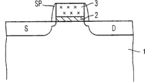
根据图4,源区S、漏区D以及源区和漏区之间的沟道区设置在半导体衬底1中。根据本发明,高k介电膜2用作栅极电介质,并形成在沟道区上,而栅极层形成在所述栅极电介质2上。此外,在栅极堆叠的侧壁处可设置隔离物SP,以形成源区和漏区S和D。当栅极层3优选包括多晶硅时,它还可以构成金属栅极,由此改善半导体器件的电特性。According to FIG. 4 , a source region S, a drain region D and a channel region between the source region and the drain region are arranged in the
图5示出半导体器件的部分截面图,其中高k介电膜用作电容器电介质。FIG. 5 shows a partial cross-sectional view of a semiconductor device in which a high-k dielectric film is used as a capacitor dielectric.
根据图5,为了例如在DRAM(动态随机存取存储器)半导体器件中实现所谓的沟槽电容器,在硅衬底1内设置深沟槽或孔。在沟槽的下部附近的衬底1中形成第二电极5之后,在沟槽或孔的表面上设置高k介电膜2。填充材料4用作所得到的电容器的第一电极,其通常是高掺杂的多晶硅或淀积的金属。According to FIG. 5 , deep trenches or holes are provided in the
由此,新的高k介电膜显著改善了半导体器件的电特性,由此能够实现进一步的集成密度。Thus, the new high-k dielectric film significantly improves the electrical characteristics of semiconductor devices, thereby enabling further integration density.
得益于该公开的本领域的技术人员应当理解,本发明被认为能提供高k介电膜,及其形成方法和相关的半导体器件,其具有通过降低隧穿电流产生的改善的漏电流以及改善的扩散阻挡特性。本发明的各个方面的另外的修改和替换实施例将由于该描述而对本领域的技术人员而显而易见。Those skilled in the art having the benefit of this disclosure will appreciate that the present invention is believed to provide high-k dielectric films, methods of forming the same, and related semiconductor devices having improved leakage current through reduced tunneling current and Improved diffusion barrier properties. Additional modifications and alternative embodiments of the various aspects of the invention will be apparent to those skilled in the art in view of this description.
附图标记列表List of reference signs
1 衬底1 Substrate
2 高k介电膜2 High-k dielectric film
3 栅极层3 gate layer
4 第一电极4 first electrode
5 第二电极5 second electrode
B 底层B Bottom
M 中间层M middle layer
T 顶层T top layer
B1 预底层B1 pre-bottom
M1 预中间层M1 pre-middle layer
T1 预顶层T1 pre-top
I 衬底界面层I Substrate interface layer
S 源区S source region
D 漏区D Drain
SP 隔离物SP separator
Claims (20)
Applications Claiming Priority (1)
| Application Number | Priority Date | Filing Date | Title |
|---|---|---|---|
| PCT/EP2003/050352 WO2005015621A1 (en) | 2003-07-30 | 2003-07-30 | High-k dielectric film, method of forming the same and related semiconductor device |
Publications (2)
| Publication Number | Publication Date |
|---|---|
| CN1820355A CN1820355A (en) | 2006-08-16 |
| CN100431103C true CN100431103C (en) | 2008-11-05 |
Family
ID=34129909
Family Applications (1)
| Application Number | Title | Priority Date | Filing Date |
|---|---|---|---|
| CNB038268728A Expired - Fee Related CN100431103C (en) | 2003-07-30 | 2003-07-30 | High-k dielectric films, methods of forming the same, and related semiconductor devices |
Country Status (6)
| Country | Link |
|---|---|
| US (3) | US7405482B2 (en) |
| EP (1) | EP1649501B1 (en) |
| CN (1) | CN100431103C (en) |
| AU (1) | AU2003266410A1 (en) |
| DE (1) | DE60311016T2 (en) |
| WO (1) | WO2005015621A1 (en) |
Families Citing this family (20)
| Publication number | Priority date | Publication date | Assignee | Title |
|---|---|---|---|---|
| US7087480B1 (en) * | 2002-04-18 | 2006-08-08 | Taiwan Semiconductor Manufacturing Company, Ltd. | Process to make high-k transistor dielectrics |
| JP4536333B2 (en) * | 2003-04-03 | 2010-09-01 | 忠弘 大見 | Semiconductor device and manufacturing method thereof |
| KR100889362B1 (en) | 2004-10-19 | 2009-03-18 | 삼성전자주식회사 | Transistor composed of multilayer dielectric film and method of manufacturing same |
| US7879739B2 (en) * | 2006-05-09 | 2011-02-01 | Intel Corporation | Thin transition layer between a group III-V substrate and a high-k gate dielectric layer |
| US7799669B2 (en) * | 2007-04-27 | 2010-09-21 | Texas Instruments Incorporated | Method of forming a high-k gate dielectric layer |
| DE102007002962B3 (en) * | 2007-01-19 | 2008-07-31 | Qimonda Ag | Method for producing a dielectric layer and for producing a capacitor |
| JP2008205065A (en) * | 2007-02-19 | 2008-09-04 | Toshiba Corp | Semiconductor device and manufacturing method thereof |
| US20080242012A1 (en) * | 2007-03-28 | 2008-10-02 | Sangwoo Pae | High quality silicon oxynitride transition layer for high-k/metal gate transistors |
| KR100877100B1 (en) * | 2007-04-16 | 2009-01-09 | 주식회사 하이닉스반도체 | Nonvolatile Memory Device Manufacturing Method |
| JP2009071232A (en) * | 2007-09-18 | 2009-04-02 | Elpida Memory Inc | Semiconductor device and manufacturing method thereof |
| US7671394B2 (en) * | 2007-10-17 | 2010-03-02 | International Business Machines Corporation | Embedded trench capacitor having a high-k node dielectric and a metallic inner electrode |
| US20120001179A1 (en) * | 2010-07-02 | 2012-01-05 | Semiconductor Energy Laboratory Co., Ltd. | Semiconductor device |
| US8786012B2 (en) | 2010-07-26 | 2014-07-22 | Infineon Technologies Austria Ag | Power semiconductor device and a method for forming a semiconductor device |
| US8614478B2 (en) | 2010-07-26 | 2013-12-24 | Infineon Technologies Austria Ag | Method for protecting a semiconductor device against degradation, a semiconductor device protected against hot charge carriers and a manufacturing method therefor |
| US8779838B2 (en) | 2011-10-25 | 2014-07-15 | International Business Machines Corporation | Methodology and apparatus for tuning driving current of semiconductor transistors |
| US9595593B2 (en) | 2015-06-29 | 2017-03-14 | Taiwan Semiconductor Manufacturing Co., Ltd. | Semiconductor structure with interfacial layer and method for manufacturing the same |
| JP6640762B2 (en) * | 2017-01-26 | 2020-02-05 | 株式会社東芝 | Semiconductor device |
| TWI634468B (en) * | 2017-08-18 | 2018-09-01 | Industrial Technology Research Institute | Transparent display device |
| CN110391231B (en) | 2018-04-16 | 2020-09-22 | 联华电子股份有限公司 | Semiconductor device and method of making the same |
| US11961895B2 (en) | 2021-09-08 | 2024-04-16 | International Business Machines Corporation | Gate stacks with multiple high-κ dielectric layers |
Citations (2)
| Publication number | Priority date | Publication date | Assignee | Title |
|---|---|---|---|---|
| US6291866B1 (en) * | 1997-07-24 | 2001-09-18 | Texas Instruments Incorporated | Zirconium and/or hafnium oxynitride gate dielectric |
| US20030129826A1 (en) * | 2000-03-07 | 2003-07-10 | Werkhoven Christiaan J. | Graded thin films |
Family Cites Families (21)
| Publication number | Priority date | Publication date | Assignee | Title |
|---|---|---|---|---|
| US5876788A (en) * | 1997-01-16 | 1999-03-02 | International Business Machines Corporation | High dielectric TiO2 -SiN composite films for memory applications |
| US5834353A (en) * | 1997-10-20 | 1998-11-10 | Texas Instruments-Acer Incorporated | Method of making deep sub-micron meter MOSFET with a high permitivity gate dielectric |
| US6693051B2 (en) * | 2001-02-01 | 2004-02-17 | Lucent Technologies Inc. | Silicon oxide based gate dielectric layer |
| US20020102797A1 (en) * | 2001-02-01 | 2002-08-01 | Muller David A. | Composite gate dielectric layer |
| JP3944367B2 (en) * | 2001-02-06 | 2007-07-11 | 松下電器産業株式会社 | Method for forming insulating film and method for manufacturing semiconductor device |
| US6960537B2 (en) * | 2001-10-02 | 2005-11-01 | Asm America, Inc. | Incorporation of nitrogen into high k dielectric film |
| US20030111678A1 (en) * | 2001-12-14 | 2003-06-19 | Luigi Colombo | CVD deposition of M-SION gate dielectrics |
| US6586349B1 (en) * | 2002-02-21 | 2003-07-01 | Advanced Micro Devices, Inc. | Integrated process for fabrication of graded composite dielectric material layers for semiconductor devices |
| US6693004B1 (en) * | 2002-02-27 | 2004-02-17 | Advanced Micro Devices, Inc. | Interfacial barrier layer in semiconductor devices with high-K gate dielectric material |
| US6682973B1 (en) * | 2002-05-16 | 2004-01-27 | Advanced Micro Devices, Inc. | Formation of well-controlled thin SiO, SiN, SiON layer for multilayer high-K dielectric applications |
| US6825538B2 (en) * | 2002-11-20 | 2004-11-30 | Agere Systems Inc. | Semiconductor device using an insulating layer having a seed layer |
| EP1487013A3 (en) * | 2003-06-10 | 2006-07-19 | Samsung Electronics Co., Ltd. | SONOS memory device and method of manufacturing the same |
| US20050153571A1 (en) * | 2003-11-17 | 2005-07-14 | Yoshihide Senzaki | Nitridation of high-k dielectric films |
| US7045432B2 (en) * | 2004-02-04 | 2006-05-16 | Freescale Semiconductor, Inc. | Method for forming a semiconductor device with local semiconductor-on-insulator (SOI) |
| US7098150B2 (en) * | 2004-03-05 | 2006-08-29 | Air Liquide America L.P. | Method for novel deposition of high-k MSiON dielectric films |
| KR100594266B1 (en) * | 2004-03-17 | 2006-06-30 | 삼성전자주식회사 | Sonos type memory device |
| KR100630680B1 (en) * | 2004-03-19 | 2006-10-02 | 삼성전자주식회사 | Non-volatile memory device having an asymmetric gate dielectric layer and method of manufacturing the same |
| KR100604846B1 (en) * | 2004-04-23 | 2006-07-31 | 삼성전자주식회사 | Memory device comprising a multilayer dielectric layer and a method of manufacturing the same |
| US7256077B2 (en) * | 2004-05-21 | 2007-08-14 | Freescale Semiconductor, Inc. | Method for removing a semiconductor layer |
| KR100660840B1 (en) * | 2004-10-08 | 2006-12-26 | 삼성전자주식회사 | Non-volatile memory device comprising a multilayer tunneling barrier layer and a method of manufacturing the same |
| US7235502B2 (en) * | 2005-03-31 | 2007-06-26 | Freescale Semiconductor, Inc. | Transitional dielectric layer to improve reliability and performance of high dielectric constant transistors |
-
2003
- 2003-07-30 CN CNB038268728A patent/CN100431103C/en not_active Expired - Fee Related
- 2003-07-30 EP EP03817953A patent/EP1649501B1/en not_active Expired - Lifetime
- 2003-07-30 AU AU2003266410A patent/AU2003266410A1/en not_active Abandoned
- 2003-07-30 DE DE60311016T patent/DE60311016T2/en not_active Expired - Lifetime
- 2003-07-30 WO PCT/EP2003/050352 patent/WO2005015621A1/en not_active Ceased
-
2006
- 2006-01-27 US US11/342,370 patent/US7405482B2/en not_active Expired - Fee Related
-
2008
- 2008-05-08 US US12/117,274 patent/US7655099B2/en not_active Expired - Fee Related
-
2009
- 2009-10-30 US US12/609,670 patent/US7923336B2/en not_active Expired - Fee Related
Patent Citations (2)
| Publication number | Priority date | Publication date | Assignee | Title |
|---|---|---|---|---|
| US6291866B1 (en) * | 1997-07-24 | 2001-09-18 | Texas Instruments Incorporated | Zirconium and/or hafnium oxynitride gate dielectric |
| US20030129826A1 (en) * | 2000-03-07 | 2003-07-10 | Werkhoven Christiaan J. | Graded thin films |
Non-Patent Citations (3)
| Title |
|---|
| ADVANCED CMOS TRANSISTORS WITH A NOVELHFSION GATE DIELECTRIC. ROTONDARO,A,L,P,ET,AL.2002 SYMPOSIUM ON VLSI TECHNOLOGY. DEGEST OF TECHNICAL PAPERS. IEEE. 2002 * |
| Effects of nitrogen in HFSiON gate dielectric on the electricaland thermal characteristics. KOYAMA M ET AL.INTERNATIONAL ELECTRON DEVICES MEETING 2002. IEDM. TECHNICAL DIGEST, IEEE. 2002 * |
| Reliability evaluation of HFSiON gate dielectric film with12.8A/sp1 deg/SiO2 equivalent thickness. SHANWARE A ET AL.INTERNATIONAL ELECTRON DEVICES MEETING 2001. IEDM. TECHNICAL DIGEST. IEEE. 2001 * |
Also Published As
| Publication number | Publication date |
|---|---|
| EP1649501A1 (en) | 2006-04-26 |
| WO2005015621A1 (en) | 2005-02-17 |
| DE60311016D1 (en) | 2007-02-15 |
| US20100047991A1 (en) | 2010-02-25 |
| US7405482B2 (en) | 2008-07-29 |
| EP1649501B1 (en) | 2007-01-03 |
| US20080246100A1 (en) | 2008-10-09 |
| US20060194451A1 (en) | 2006-08-31 |
| DE60311016T2 (en) | 2007-08-02 |
| AU2003266410A1 (en) | 2005-02-25 |
| CN1820355A (en) | 2006-08-16 |
| US7655099B2 (en) | 2010-02-02 |
| US7923336B2 (en) | 2011-04-12 |
Similar Documents
| Publication | Publication Date | Title |
|---|---|---|
| US7923336B2 (en) | High-k dielectric film, method of forming the same and related semiconductor device | |
| US8168547B2 (en) | Manufacturing method of semiconductor device | |
| EP1300887B1 (en) | Method of manufacturing a semiconductor device | |
| JP4165076B2 (en) | Semiconductor device having high dielectric constant insulating film | |
| TWI462298B (en) | A semiconductor device, a semiconductor device manufacturing method, and a substrate processing system | |
| US6821873B2 (en) | Anneal sequence for high-κ film property optimization | |
| KR100868768B1 (en) | CMOS semiconductor device and its manufacturing method | |
| US7586159B2 (en) | Semiconductor devices having different gate dielectrics and methods for manufacturing the same | |
| US20090057787A1 (en) | Semiconductor device | |
| KR100639673B1 (en) | Semiconductor device having a gate dielectric film made of a high-k alloy and a method of manufacturing the same | |
| JP2004214661A (en) | Fabrication of transistor gate and method for reducing roughness of high-k gate dielectric | |
| JP2004259906A (en) | Semiconductor device and manufacturing method thereof | |
| JP2005064523A (en) | Capacitor for semiconductor device, method for manufacturing the same, and memory device including the capacitor | |
| US8294201B2 (en) | High-k gate dielectric and method of manufacture | |
| US20050142715A1 (en) | Semiconductor device with high dielectric constant insulator and its manufacture | |
| US8633119B2 (en) | Methods for manufacturing high dielectric constant films | |
| JP3581354B2 (en) | Field effect transistor | |
| US20040169240A1 (en) | Semiconductor device and method of manufacturing semiconductor device | |
| US7741684B2 (en) | Semiconductor device and method for fabricating the same | |
| JP2004247474A (en) | Semiconductor device, manufacturing method thereof, and film forming method | |
| JP2004289082A (en) | Method of forming high dielectric constant gate insulating film | |
| KR100616500B1 (en) | Gate electrode of semiconductor device and manufacturing method thereof | |
| JP2005079306A (en) | Method for manufacturing semiconductor device | |
| JP4220991B2 (en) | Manufacturing method of semiconductor device | |
| TW202548896A (en) | Semiconductor device and manufacturing method thereof |
Legal Events
| Date | Code | Title | Description |
|---|---|---|---|
| C06 | Publication | ||
| PB01 | Publication | ||
| C10 | Entry into substantive examination | ||
| SE01 | Entry into force of request for substantive examination | ||
| C14 | Grant of patent or utility model | ||
| GR01 | Patent grant | ||
| CF01 | Termination of patent right due to non-payment of annual fee | ||
| CF01 | Termination of patent right due to non-payment of annual fee |
Granted publication date: 20081105 Termination date: 20180730 |