CN100505103C - Shift buffer and flat panel display using the same - Google Patents
Shift buffer and flat panel display using the same Download PDFInfo
- Publication number
- CN100505103C CN100505103C CNB2005100661715A CN200510066171A CN100505103C CN 100505103 C CN100505103 C CN 100505103C CN B2005100661715 A CNB2005100661715 A CN B2005100661715A CN 200510066171 A CN200510066171 A CN 200510066171A CN 100505103 C CN100505103 C CN 100505103C
- Authority
- CN
- China
- Prior art keywords
- signal
- phase inverter
- clock
- clock signal
- circuit
- Prior art date
- Legal status (The legal status is an assumption and is not a legal conclusion. Google has not performed a legal analysis and makes no representation as to the accuracy of the status listed.)
- Expired - Fee Related
Links
- 239000000872 buffer Substances 0.000 title claims abstract description 30
- 239000011159 matrix material Substances 0.000 claims description 13
- 239000004973 liquid crystal related substance Substances 0.000 claims description 9
- 239000000758 substrate Substances 0.000 claims description 7
- 230000000630 rising effect Effects 0.000 claims description 4
- 239000000463 material Substances 0.000 claims 7
- 230000007423 decrease Effects 0.000 claims 1
- 230000001360 synchronised effect Effects 0.000 claims 1
- 102100040862 Dual specificity protein kinase CLK1 Human genes 0.000 description 24
- 102100040844 Dual specificity protein kinase CLK2 Human genes 0.000 description 13
- 101000749294 Homo sapiens Dual specificity protein kinase CLK1 Proteins 0.000 description 13
- 101000749291 Homo sapiens Dual specificity protein kinase CLK2 Proteins 0.000 description 13
- 238000000034 method Methods 0.000 description 8
- 238000010586 diagram Methods 0.000 description 6
- 229910021420 polycrystalline silicon Inorganic materials 0.000 description 6
- 230000000295 complement effect Effects 0.000 description 5
- 239000010409 thin film Substances 0.000 description 5
- 229920005591 polysilicon Polymers 0.000 description 4
- 230000008569 process Effects 0.000 description 4
- 239000011521 glass Substances 0.000 description 3
- 230000008859 change Effects 0.000 description 2
- 239000012528 membrane Substances 0.000 description 2
- 235000013446 pixi Nutrition 0.000 description 2
- 239000004065 semiconductor Substances 0.000 description 2
- 230000003068 static effect Effects 0.000 description 2
- 230000001934 delay Effects 0.000 description 1
- 238000005401 electroluminescence Methods 0.000 description 1
- 230000006870 function Effects 0.000 description 1
- 230000007257 malfunction Effects 0.000 description 1
- 230000004048 modification Effects 0.000 description 1
- 238000012986 modification Methods 0.000 description 1
- 230000007704 transition Effects 0.000 description 1
Images


Classifications
-
- G—PHYSICS
- G11—INFORMATION STORAGE
- G11C—STATIC STORES
- G11C19/00—Digital stores in which the information is moved stepwise, e.g. shift registers
-
- G—PHYSICS
- G11—INFORMATION STORAGE
- G11C—STATIC STORES
- G11C19/00—Digital stores in which the information is moved stepwise, e.g. shift registers
- G11C19/28—Digital stores in which the information is moved stepwise, e.g. shift registers using semiconductor elements
Landscapes
- Control Of Indicators Other Than Cathode Ray Tubes (AREA)
- Shift Register Type Memory (AREA)
- Liquid Crystal Display Device Control (AREA)
- Control Of El Displays (AREA)
Abstract
Description
技术领域 technical field
本发明是有关于一种移位缓存器。The invention relates to a shift register.
背景技术 Background technique
移位缓存器是一种周知的顺序逻辑电路,主要用于暂存和传输资料信号。一个典型的移位缓存器包括在一炼中连结在一起的闩锁电路或正反电路的级/组,使得一级电路的输出成为下一级电路的输入。移位缓存器中的每一级电路通常由一个或多个时钟信号驱动。缓存器广泛用于各种类型的电子设备,例如平板显示器。A shift register is a well-known sequential logic circuit mainly used for temporarily storing and transmitting data signals. A typical shift register consists of stages/groups of latch circuits or flip-flop circuits connected together in a chain so that the output of one stage becomes the input of the next stage. Each stage of circuitry in a shift register is typically driven by one or more clock signals. Buffers are widely used in various types of electronic devices, such as flat panel displays.
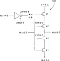
图3所示为习知的移位缓存器电路300。如图所示,移位缓存器300接收启动信号ST,其依序传输S个级,从闩锁电路Latch1传到LatchS。移位缓存器300还配置来用以输出信号OUT1~OUTs。移位缓存器300基于一时钟信号CLK和一反相时钟信号CLK(下文中称为“XCLK”)而工作,其中XCLK是藉由将时钟信号CLK反相而获得的。互补时钟信号,例如CLK和XCLK,是由于其元件的工作特性而用于习知的移位缓存器中。FIG. 3 shows a conventional
图4A为习知的移位缓存器400的详细示意图。如图所示,移位缓存器400处理一资料信号ST,并基于时钟信号CLK和XCLK而工作。移位缓存器400由两级相邻的闩锁电路410和420组成。闩锁电路410包括一个反相器413和两个时脉反相器411和415。闩锁电路420包括一个反相器423和两个时脉反相器421和425。在闩锁电路410和420中,反相器413和415以及423和425分别连接在一起而形成一个正反器电路。FIG. 4A is a detailed schematic diagram of a
下面来描述移位缓存器400的工作情况。其为将信号ST送给闩锁电路410的时脉反相器411,并经由反相器413传给下一个闩锁电路420。在闩锁电路410和420的反相器413或者423的输出端可以分别获得输出信号组OUTk和OUTk+1。The operation of the
为了控制信号ST通过移位缓存器400的过程,因而闩锁电路410和420会根据一个或者多个时钟信号的上升和下降依序闩锁信号ST。特别地,闩锁电路410和420为由两个时钟信号CLK和XCLK控制。时钟信号CLK和XCLK分别供给闩锁电路410和420的时脉反相器411、415和421和425。In order to control the process of the signal ST passing through the
图4B所示为一例时钟信号CLK和XCLK。如图所示,时钟信号CLK和XCLK相位相反,并具有50%的工作周期。互补时钟信号,例如是CLK和XCLK,由于其时脉反相器的工作特性,而被用于习知的移位缓存器中。闩锁电路410和420中的时脉反相器,例如时脉反相器411、415、421和425,其内部结构和工作情况则描述于以下的图5。FIG. 4B shows an example of clock signals CLK and XCLK. As shown, the clock signals CLK and XCLK are opposite in phase and have a 50% duty cycle. Complementary clock signals, such as CLK and XCLK, are used in conventional shift registers due to their clocked inverter nature. The internal structure and operation of the clock inverters in the
图5所示为习知时脉反相器的一个例子,例如,时脉反相器411、415、421和425。特别地,如一时脉反相器500所示,其处理输入信号IN的方式为基于一组互补时钟信号CKN和CKP产生一输出信号OUT。典型地,时脉反相器500由两个P型金属氧化物半导体(“PMOS”)晶体管M1、M2以及两个N型金属氧化物半导体(“NMOS”)晶体管M3和M4构成。FIG. 5 shows an example of conventional clock inverters, for example,
输入信号IN为传送给PMOS晶体管M1和NMOS晶体管M4。同样,时钟信号CKP和CKN分别传送给PMOS晶体管M2和NMOS晶体管M3。时钟信号CKP和CKN与CLK和XCLK(前面已经于图4描述过)具有相同的波形。即,CKP和CKN也是具有相反相位和50%的工作周期信号。随着时钟信号CKP和CKN由高变到低及由低变到高,晶体管M2和M3闸控输入信号IN到其输出。然后可以在PMOS晶体管M2和NMOS晶体管M3之间获得一输出信号OUT。因此,习知的移位缓存器电路中的时脉反相器的工作为取决于一组互补时钟信号。The input signal IN is sent to the PMOS transistor M1 and the NMOS transistor M4. Likewise, the clock signals CKP and CKN are transmitted to the PMOS transistor M2 and the NMOS transistor M3, respectively. The clock signals CKP and CKN have the same waveform as CLK and XCLK (described earlier in FIG. 4 ). That is, CKP and CKN are also signals with opposite phases and 50% duty cycle. Transistors M2 and M3 gate the input signal IN to their outputs as the clock signals CKP and CKN transition from high to low and from low to high. An output signal OUT can then be obtained between the PMOS transistor M2 and the NMOS transistor M3. Therefore, the operation of the clocked inverter in the conventional shift register circuit depends on a set of complementary clock signals.
由于习知的移位缓存器使用相位相反并具有50%的工作周期的互补时钟信号,所以其对时钟信号的变化或抖动比较敏感。时钟信号的变化可以由各种因素引起,例如闸控延迟、时脉线路的特性或者温度的变化。Since the conventional shift register uses complementary clock signals with opposite phases and a 50% duty cycle, it is sensitive to variations or jitters of the clock signals. Variations in the clock signal can be caused by various factors, such as gating delays, characteristics of the clock line, or changes in temperature.
请参阅图6所示,其为时脉抖动或变化的一个例子。如图所示,在时间T1中,时钟信号CKP的相位由逻辑高准位变为逻辑低准位。然而,由于延迟,时钟信号CKN的相位并不从逻辑低准位变为逻辑高准位,而是在延迟t时间后开始改变其相位。CKN相对于CKP的延迟,例如会引起晶体管M2相对于晶体管M3工作不同步。这样,或许就会导致从时脉反相器500和/或移位缓存器400的输出信号错误。因而,时钟信号之间的相位变化可以造成习知的缓存器的不正常工作或甚至是失效。See Figure 6 for an example of clock jitter or variation. As shown in the figure, at time T1, the phase of the clock signal CKP changes from a logic high level to a logic low level. However, due to the delay, the phase of the clock signal CKN does not change from a logic low level to a logic high level, but starts to change its phase after a delay of t time. The delay of CKN relative to CKP, for example, will cause the transistor M2 to operate asynchronously relative to the transistor M3. In this way, the output signal from the
因而需要提供一种移位缓存器,其能够容许时钟信号的变化。Therefore, it is desirable to provide a shift register that can tolerate changes in the clock signal.
发明内容 Contents of the invention
根据本发明的实施例,一个移位缓存器包括多数级。每一级包括相应的闩锁电路,该闩锁电路包含一第一时脉反相器和一闩锁电路。该第一时脉反相器由一第一时钟信号和一第二时钟信号控制将输入信号反相,并且该反相后的输入信号由闩锁电路闩锁。该闩锁输入信号作为后序级的输入信号。在上述的多数级的偶数级,一第一反相器设置于上述的第一时脉反相器的输入端之前,将输入信号反相以用于相应的闩锁电路,同时一第二反相器设置于该闩锁电路的输出端之后,将该闩锁的输入信号反相,以作为在该偶数级中相应的闩锁电路的输出信号。According to an embodiment of the present invention, a shift register includes a plurality of stages. Each stage includes a corresponding latch circuit including a first clocked inverter and a latch circuit. The first clock inverter is controlled by a first clock signal and a second clock signal to invert the input signal, and the inverted input signal is latched by the latch circuit. This latch input signal is used as the input signal of the subsequent stage. In the even-numbered stages of the above-mentioned multiple stages, a first inverter is arranged before the input terminal of the above-mentioned first clock inverter, and inverts the input signal for the corresponding latch circuit, while a second inverter An invertor is arranged after the output terminal of the latch circuit, and inverts the input signal of the latch to serve as the output signal of the corresponding latch circuit in the even stage.
根据本发明的其他实施例,其为提供一种移位缓存器,将一数字信号与一第一时钟信号和一第二时钟信号同步依序进行传输。该移位缓存器包括多数个依序串联的级。每一级包括相应的闩锁单元,每个闩锁单元基于上述的第一时钟信号和第二时钟信号,对应于输入信号输出一信号。该输出信号用于后序级作为后序级闩锁单元的输入信号。在上述的多数级的偶数级,在闩锁单元的输入端之前设置有一第一反相器,将该输入信号进行反相,以用于相应的闩锁单元。在该闩锁单元的输出端之后设置有一第二反相器,以将该闩锁单元的输出进行反相,并作为在偶数级相应的闩锁电路的输出信号。According to other embodiments of the present invention, a shift register is provided, which sequentially transmits a digital signal synchronously with a first clock signal and a second clock signal. The shift register includes a plurality of stages connected in series. Each stage includes a corresponding latch unit, and each latch unit outputs a signal corresponding to the input signal based on the above-mentioned first clock signal and second clock signal. This output signal is used in the subsequent stage as an input signal of the latch unit of the subsequent stage. In the above-mentioned even-numbered stages of the plurality of stages, a first inverter is provided before the input terminal of the latch unit, and the input signal is inverted to be used for the corresponding latch unit. A second inverter is arranged after the output terminal of the latch unit to invert the output of the latch unit and serve as the output signal of the corresponding latch circuit in the even stage.
根据本发明的另外其他的实施例,移位缓存器基于一第一时钟信号和一第二时钟信号来处理一输入信号。该移位缓存器包括一第一级和一第二级。该第一级包括一第一闩锁电路,基于第一和第二时钟信号将该输入信号闩锁。该第二级包括一第一反相器,将该第一级的输出进行反相,一第二闩锁电路,耦接到该第一反相器,以及一第二反相器,将第二闩锁电路的输出进行反相。According to still other embodiments of the present invention, the shift register processes an input signal based on a first clock signal and a second clock signal. The shift register includes a first stage and a second stage. The first stage includes a first latch circuit that latches the input signal based on the first and second clock signals. The second stage includes a first inverter for inverting the output of the first stage, a second latch circuit coupled to the first inverter, and a second inverter for inverting the first The outputs of the two latch circuits are inverted.
为让本发明的上述和其他目的、特征和优点能更明显易懂,下文特举较佳实施例,并配合所附图式,作详细说明如下。In order to make the above and other objects, features and advantages of the present invention more comprehensible, preferred embodiments will be described in detail below together with the accompanying drawings.
附图说明 Description of drawings
图1绘示依照本发明一较佳实施例的一种显示器(下文中称为“Poly-SiTFT LCD”)的方块示意图。FIG. 1 shows a schematic block diagram of a display (hereinafter referred to as "Poly-SiTFT LCD") according to a preferred embodiment of the present invention.
图2A绘示依照本发明一较佳实施例的一种多晶硅薄膜晶体管液晶显示器(Poly-Si TFT LCD)的方块示意图。FIG. 2A shows a schematic block diagram of a polysilicon thin film transistor liquid crystal display (Poly-Si TFT LCD) according to a preferred embodiment of the present invention.
图2B绘示依照本发明一较佳实施例的一种资料驱动电路。FIG. 2B illustrates a data driving circuit according to a preferred embodiment of the present invention.
图2C绘示依照本发明一较佳实施例的一种闸极驱动电路。FIG. 2C illustrates a gate driving circuit according to a preferred embodiment of the present invention.
图3绘示为习知移位缓存器的方块示意图。FIG. 3 is a schematic block diagram of a conventional shift register.
图4A绘示为图3中的移位缓存器中的两个相邻的闩锁电路。FIG. 4A shows two adjacent latch circuits in the shift register in FIG. 3 .
图4B绘示为用于图4A的闩锁电路的时钟信号。FIG. 4B illustrates clock signals for the latch circuit of FIG. 4A.
图5绘示为习知实施于图4所示的闩锁电路的时脉反相器。FIG. 5 shows a conventional clocked inverter implemented in the latch circuit shown in FIG. 4 .
图6绘示为用于图4A的闩锁电路的时钟信号。FIG. 6 illustrates clock signals for the latch circuit of FIG. 4A.
图7为绘示依照本发明一较佳实施例的一种移位缓存器的相邻闩锁电路。FIG. 7 illustrates an adjacent latch circuit of a shift register according to a preferred embodiment of the present invention.
图8和图9为绘示依照本发明一较佳实施例的一种用于图7所示的移位缓存器的闩锁电路的时钟信号。8 and 9 illustrate clock signals of a latch circuit for the shift register shown in FIG. 7 according to a preferred embodiment of the present invention.
图10为绘示依照本发明一较佳实施例的一种用于显示器中的资料驱动电路或者闸极驱动电路的移位缓存器。FIG. 10 is a diagram illustrating a shift register used in a data driving circuit or a gate driving circuit in a display according to a preferred embodiment of the present invention.
100:显示器 105、205:玻璃基板100:
110、210:资料驱动电路120、220:闸极驱动电路110, 210: data drive
130:端部 140:膜缆线130: End 140: Membrane cable
150:积体印刷电路板 200:显示装置150: Integrated printed circuit board 200: Display device
207:像素阵列207: pixel array
230、260、400、700、1000:移位缓存器230, 260, 400, 700, 1000: shift register
240、270:准位转换器 250、280:缓冲器240, 270: level converter 250, 280: buffer
300:移位缓存器电路 400:准位转换器300: Shift register circuit 400: Level converter
410、420、710、720:闩锁电路410, 420, 710, 720: Latch circuit
411、415、421、425、500、711、715、721、725:时脉反相器411, 415, 421, 425, 500, 711, 715, 721, 725: clock inverter
413、423、713、723:反相器 730:第一反相器413, 423, 713, 723: inverter 730: first inverter
740:第二反相器 M1、M2、M3、M4:晶体管740: second inverter M1, M2, M3, M4: transistors
具体实施方式 Detailed ways
本发明的多个实施例提出一种移位缓存器,其可容忍时钟信号的变化和抖动。符合本发明原理的移位缓存器可以用于显示器(例如,平板显示器)的驱动电路。在一些实施例中,该移位缓存器包括多级闩锁电路。在偶数级闩锁电路的输入和输出可以配置有反相器。另外,移位缓存器可以基于两个不同的时钟信号而工作。这两个时钟信号可以具有非50%的工作周期,并且可以随意地彼此重迭。Various embodiments of the present invention propose a shift register that is tolerant to clock signal variation and jitter. A shift register consistent with the principles of the present invention can be used in a drive circuit for a display (eg, a flat panel display). In some embodiments, the shift register includes multi-stage latch circuits. Inverters can be configured at the input and output of the even-numbered-stage latch circuit. Additionally, the shift register can operate on two different clock signals. These two clock signals can have a duty cycle other than 50%, and can optionally overlap each other.
下面结合附图对本发明的实施例进行详细的描述。所有附图中相同或者相似的部分使用相同的参考标号。Embodiments of the present invention will be described in detail below in conjunction with the accompanying drawings. The same reference numerals are used for the same or similar parts in all the drawings.
图1是一例显示器100。显示器100可以为任意类型的显示器,例如平板显示器。在本领域的技术人员可知,其他类型的显示器,例如阴极射线管(CRT)显示器、液晶显示器(LED),和其他类型的等离子显示器,都符合本发明的原理。例如,显示器100可以实施在有机电发光显示器(OLED),场发光显示器(FED)、等离子显示面板(PDP)等FIG. 1 is an example of a
为了便于叙述,以显示器100实施在多晶硅薄膜晶体管液晶显示器(Poly-Si TFT平板显示器)来描述。特别地,显示器100包括形成于玻璃基板105上的资料驱动电路110和闸极驱动电路120。端部130与积体印刷电路板(PCB)150用一膜缆线140连接。For ease of description, it is described that the
图2A是多晶硅薄膜晶体管液晶显示器200的详细示意图。特别地,图2A为绘示多晶硅薄膜晶体管液晶显示装置200的结构。显示装置200可以包括具有像素阵列207的玻璃基板205、资料驱动电路210和闸极驱动电路220。FIG. 2A is a detailed schematic diagram of a polysilicon thin film transistor
如图2A所示,资料驱动电路210可以耦接到具有M条资料信号线DL1~DLM的像素阵列207。闸极驱动电路220也可以经由N条扫描信号线GL1~GLN耦接到像素阵列207。在像素阵列207中,在每条资料信号线DLi(其中,i为1~M之间的整数)与每条扫描信号线GLj(其中,j为1~N之间的整数)的交叉处,形成一像素PIXi,j。资料驱动电路210和闸极驱动电路220可以基于各种矩阵架构(例如,单矩阵或双矩阵)耦接到像素阵列。As shown in FIG. 2A , the
在一些实施例中,资料驱动电路210和闸极驱动电路220可以基于主动矩阵定址来定址像素PIXi,j。但是,其他类型的定址可以由本发明的其他实施例支援。例如,符合本发明原理的显示器还可以使用被动矩阵定址。In some embodiments,
在一些实施例中,驱动电路210和220为由薄膜晶体管制成而积体于显示器200中。当然,本领域的技术人员可知,驱动电路210和220可以使用硬体、软体、韧体或者其组合的元件来实施。以下分别参照图2B和图2C来说明资料驱动电路210和闸极驱动电路220的结构。In some embodiments, the driving
图2B所示为资料驱动电路210的基本结构。如图所示,资料驱动电路210可以包括移位缓存器230、准位转换器(level shifter)240、以及缓冲器250。下面将对这些组件进一步描述。FIG. 2B shows the basic structure of the
移位缓存器230接收一启动信号STD,并基于时钟信号CKD将其传输以用于显示器。移位缓存器230可以基于周知的方法(例如,逐点驱动方法或者逐线驱动方法)而工作。移位缓存器230可以用周知的元件来实施和配置。例如,在一实施例中,移位缓存器可以静态移位缓存器来实施。The shift register 230 receives a start signal STD and transmits it based on the clock signal CKD for the display. The shift register 230 may operate based on a known method (for example, a dot-by-dot driving method or a line-by-line driving method). The shift register 230 can be implemented and configured with well-known components. For example, in one embodiment, the shift register may be implemented as a static shift register.
准位转换器240将来自移位缓存器230的信号调整为可以启动开关元件的准位。准位转换器240可以用周知的元件来实施。The level converter 240 adjusts the signal from the shift register 230 to a level that can activate the switch element. The level shifter 240 can be implemented with known components.
缓冲器250是可选择的,并且能够控制到像素阵列207(例如,到线DL1~DLM)的显示资料的顺序。缓冲器250还可以使用周知的元件来实施。Buffer 250 is optional and can control the order of display data to pixel array 207 (eg, to lines DL1-DLM). Buffer 250 may also be implemented using well-known components.
图2C所示为闸极驱动电路220的基本结构。如图所示,闸极驱动电路可以包括移位缓存器260、准位转换器270和缓冲器280。FIG. 2C shows the basic structure of the
移位缓存器260接收启动信号STS,并基于时钟信号CKS将其传输用于显示器。移位缓存器260可以用周知的元件来实施和配置。例如,在一些实施例中,移位缓存器260可以静态移位缓存器来实施。The shift register 260 receives the start signal STS and transmits it for the display based on the clock signal CKS. The shift register 260 can be implemented and configured using well-known components. For example, in some embodiments, shift register 260 may be implemented as a static shift register.
准位转换器270将来自移位缓存器260的信号调整为不同的准位。准位转换器270可以用周知的元件来实施。The level converter 270 adjusts the signal from the shift register 260 to different levels. The level shifter 270 can be implemented with known components.
缓冲器280可以控制送给像素阵列207(例如,线GL1~GLN)的驱动信号的顺序,缓冲器280还可以用周知的元件来实施。The buffer 280 can control the sequence of driving signals sent to the pixel array 207 (for example, the lines GL1-GLN), and the buffer 280 can also be implemented with well-known components.
当然,本领域的技术人员可知,在资料驱动电路210和闸极驱动电路220中,可以包括各种其他元件。例如,驱动电路210和220还可以包括元件,例如,模/数转换器和记忆体(即存储介质,以下均称为记忆体)。Certainly, those skilled in the art know that various other elements may be included in the
图7所示为符合本发明实施例的移位缓存器700。在一些实施例中,移位缓存器700可以用于前述的资料驱动电路210和闸极驱动电路220。另外,在一些实施例中,移位缓存器700的多个级可以为受限反相器,以容忍时脉变化和时脉抖动。例如,该些反相器可以用作阻止由时脉变化所引起的错误而必须的缓冲器或延迟元件。另外,该些反相器可以用于将由时脉变化或抖动引起的错误孤立只在一级。下面将描述该些有界反相器的应用例。FIG. 7 shows a
在一些实施例中,移位缓存器700的奇数级(例如,1,3,5级等)可以包括一闩锁电路,该闩锁电路基于两个时钟信号而工作。然而,在移位缓存器700奇数级和偶数级(例如,级2,4,6等)之间可以配置有反相器。例如,如图7所示,在闩锁电路710的输出端和闩锁电路720的输入端之间配置有一反相器730。在移位缓存器700的输出闩锁电路720和移位缓存器700的下一级之间配置有一第二反相器740。该架构对于设置每个闩锁电路的每个输入信号的相位为彼此相同是有效的。In some embodiments, odd stages (eg, stages 1, 3, 5, etc.) of the
另外,如上所述,移位缓存器700可以基于两个时钟信号而工作。在各个实施例中,该两个时钟信号的工作周期可以配置为非50%,而且,该两个时钟信号可以在任意数量的逻辑低准位重迭(0-0重迭)或逻辑高准位重迭(1-1重迭)。In addition, as described above, the
如图所示,移位缓存器700可以包括相邻的闩锁电路710和720。在闩锁电路710和720之间可以设置有一第一反相器730。另外,在闩锁电路720和移位缓存器700的下一级(图中未示)之间可以设置有一第二反相器740。As shown,
闩锁电路710可以包括一反相器713和两个时脉反相器711和715。如图所示,反相器713和时脉反相器715连接在一起形成一个正反电路。在工作期间,启动信号ST传送给时脉反相器711,并经由反相器713传送给移位缓存器700的下一级。在时脉反相器711和715的控制端配置有一第一时钟信号CLK1和一第二时钟信号CLK2。这样,闩锁电路710将闩锁从前面的闩锁电路(图中未绘示)所接收的启动信号ST,并且回应两个时钟信号CLK1和CLK2的上升和下降,将闩锁的信号传送给后序的闩锁电路(例如,闩锁电路720)。从闩锁电路710所得的输出OUTk还可以从反相器713的输出获得。The
闩锁电路720可以包括一个反相器723和两个时脉反相器721和725。反相器723和时脉反相器725连接形成一正反电路。在工作期间,将闩锁电路710的输出用作闩锁电路720的输入。在一些实施例中,闩锁电路710的输出首先由第一反相器730进行反相,然后输入到闩锁电路720的时脉反相器721。与闩锁电路710类似,闩锁电路720可以基于两个时钟信号CLK1和CLK2的上升和下降来工作。然后,时脉反相器721的输出被闩锁,并经由反相器723传送给下一级。然后,反相器723的输出可以由反相器740进行反相。那么就可以从反相器740的输出获得一输出信号OUTk+1。The
图8所示为一例时钟信号CLK1和CLK2的波形,其可以用于本发明的实施例中。在图示的实施例中,该第一时钟信号CLK1的工作周期小于50%,并且第二时钟信号CLK2的工作周期也小于50%。本发明的各个实施例可以使用小于50%的工作周期,以确保在这些信号的边缘之间有一定间隔或扩展。当然,本领域的技术人员可知,本发明不同的实施例可以使用其他的工作周期。在其他实施例中,时钟信号CLK1和CLK2可以任意重迭。FIG. 8 shows an example of the waveforms of clock signals CLK1 and CLK2, which can be used in embodiments of the present invention. In the illustrated embodiment, the duty cycle of the first clock signal CLK1 is less than 50%, and the duty cycle of the second clock signal CLK2 is also less than 50%. Various embodiments of the invention may use a duty cycle of less than 50% to ensure some spacing or spread between the edges of these signals. Certainly, those skilled in the art know that different embodiments of the present invention can use other duty cycles. In other embodiments, the clock signals CLK1 and CLK2 may overlap arbitrarily.
图9所示为一例时钟信号CLK1和CLK2的波形,其中这两个波形重迭。如图所示,在时间段P1,该第一时钟信号CLK1和该第二时钟信号CLK2在逻辑高准位重迭(1-1重迭)。在时间段P2,该第一时钟信号CLK1和该第二时钟信号CLK2在逻辑低准位重迭(0-0重迭)。FIG. 9 shows an example of the waveforms of the clock signals CLK1 and CLK2, where the two waveforms overlap. As shown in the figure, during the time period P1, the first clock signal CLK1 and the second clock signal CLK2 overlap at logic high levels (1-1 overlap). During the period P2, the first clock signal CLK1 and the second clock signal CLK2 overlap at logic low levels (0-0 overlap).
图10所示为符合本发明实施例的一K级移位缓存器1000的实施例。如上所述,移位缓存器1000可以实施于平板显示装置中的资料驱动电路或者闸极驱动电路中。如图所示,移位缓存器1000包括k个闩锁电路链。然而,在每个偶数级(例如,级2,4,6等),该闩锁电路包括两个附加的反相器。如上所述,该些附加反相器可以用来缓冲或者隔离由于时脉变化或抖动而产生的失误。FIG. 10 shows an embodiment of a K-
在工作期间,启动信号基于第一时钟信号CLK1和第二时钟信号CLK2依序从闩锁电路Latch1传输到Latchk(例如,为k级)。在一些实施例中,控制信号CLK1和CLK2的工作周期配置为非50%。这样,时钟信号CLK1和CLK2的边缘之间或许会有一所需的间隔或扩展。在一些实施例中,该特性用来允许缓存器1000的元件,例如PMOS或者NMOS晶体管正常工作。然而,在另一些移位缓存器1000的实施例中,该第一时钟信号CLK1和该第二时钟信号CLK2彼此任意重迭。During operation, the enable signal is sequentially transmitted from the latch circuit Latch1 to Latchk (for example, in k stages) based on the first clock signal CLK1 and the second clock signal CLK2 . In some embodiments, the duty cycle of the control signals CLK1 and CLK2 is configured to be other than 50%. Thus, there may be a desired spacing or spread between the edges of clock signals CLK1 and CLK2. In some embodiments, this feature is used to allow elements of the
虽然本发明已以较佳实施例揭露如上,然其并非用以限定本发明,任何熟习此技艺者,在不脱离本发明的精神和范围内,当可作些许的更动与润饰,因此本发明的保护范围当视后附的申请专利范围所界定者为准。Although the present invention has been disclosed above with preferred embodiments, it is not intended to limit the present invention. Anyone skilled in the art can make some changes and modifications without departing from the spirit and scope of the present invention. Therefore, this The scope of protection of the invention shall be defined by the scope of the appended patent application.
Claims (29)
Applications Claiming Priority (3)
| Application Number | Priority Date | Filing Date | Title |
|---|---|---|---|
| US58766004P | 2004-07-13 | 2004-07-13 | |
| US60/587,660 | 2004-07-13 | ||
| US10/980,781 | 2004-11-04 |
Publications (2)
| Publication Number | Publication Date |
|---|---|
| CN1758381A CN1758381A (en) | 2006-04-12 |
| CN100505103C true CN100505103C (en) | 2009-06-24 |
Family
ID=36703681
Family Applications (1)
| Application Number | Title | Priority Date | Filing Date |
|---|---|---|---|
| CNB2005100661715A Expired - Fee Related CN100505103C (en) | 2004-07-13 | 2005-04-21 | Shift buffer and flat panel display using the same |
Country Status (4)
| Country | Link |
|---|---|
| US (1) | US20060013352A1 (en) |
| JP (1) | JP2006031908A (en) |
| CN (1) | CN100505103C (en) |
| TW (1) | TWI298473B (en) |
Families Citing this family (17)
| Publication number | Priority date | Publication date | Assignee | Title |
|---|---|---|---|---|
| KR101032945B1 (en) * | 2004-03-12 | 2011-05-09 | 삼성전자주식회사 | Shift register and display device including same |
| US8115727B2 (en) * | 2006-05-25 | 2012-02-14 | Chimei Innolux Corporation | System for displaying image |
| US7750715B2 (en) * | 2008-11-28 | 2010-07-06 | Au Optronics Corporation | Charge-sharing method and device for clock signal generation |
| TW201027502A (en) * | 2009-01-15 | 2010-07-16 | Novatek Microelectronics Corp | Gate driver and display driver using thereof |
| CN102708816B (en) * | 2012-03-02 | 2013-06-12 | 京东方科技集团股份有限公司 | Shift register, grid driving device and display device |
| CN103366661A (en) * | 2012-03-30 | 2013-10-23 | 群康科技(深圳)有限公司 | An image display system and a bidirectional shift register circuit |
| JP5949213B2 (en) * | 2012-06-28 | 2016-07-06 | セイコーエプソン株式会社 | Shift register circuit, electro-optical device, and electronic apparatus |
| KR102347024B1 (en) | 2014-03-19 | 2022-01-03 | 가부시키가이샤 한도오따이 에네루기 켄큐쇼 | Semiconductor device |
| KR20160054793A (en) * | 2014-11-07 | 2016-05-17 | 에스케이하이닉스 주식회사 | Shift register circuit and memory device including the same |
| CN104361860B (en) * | 2014-11-19 | 2017-02-22 | 京东方科技集团股份有限公司 | Shift register, gate drive circuit and display device |
| US9787292B2 (en) * | 2016-01-21 | 2017-10-10 | Globalfoundries Inc. | High performance multiplexed latches |
| CN106023901B (en) * | 2016-08-03 | 2018-07-17 | 京东方科技集团股份有限公司 | Shift register cell, driving method, gate driving circuit and display device |
| DE102019106109A1 (en) | 2018-04-03 | 2019-10-10 | Taiwan Semiconductor Manufacturing Company, Ltd. | DATA MEMORY CIRCUIT AND METHOD |
| US11012057B2 (en) | 2018-04-03 | 2021-05-18 | Taiwan Semiconductor Manufacturing Company, Ltd. | Data retention circuit and method |
| TWI704493B (en) * | 2019-05-07 | 2020-09-11 | 華邦電子股份有限公司 | Bit data shifter |
| CN111986725B (en) * | 2019-05-24 | 2022-08-30 | 华邦电子股份有限公司 | Bit data shifter |
| US11177011B2 (en) | 2019-06-22 | 2021-11-16 | Winbond Electronics Corp. | Bit data shifter |
Citations (6)
| Publication number | Priority date | Publication date | Assignee | Title |
|---|---|---|---|---|
| JPH01206717A (en) | 1988-02-15 | 1989-08-18 | Hitachi Ltd | Data latch circuit and shift circuit |
| US5189315A (en) * | 1991-02-18 | 1993-02-23 | Nec Corp. | High-speed flip flop circuit with master latching circuit free from influence of slave latching circuit |
| JPH05206792A (en) | 1992-01-30 | 1993-08-13 | Nec Ic Microcomput Syst Ltd | Flip-flop circuit |
| JPH06232704A (en) | 1993-02-03 | 1994-08-19 | Nippon Steel Corp | Flip-flop circuit |
| CN1126392A (en) * | 1994-03-24 | 1996-07-10 | Dva公司 | Scannable latch and method of using the same |
| JP2000322020A (en) * | 1999-05-14 | 2000-11-24 | Sharp Corp | Bidirectional shift register and image display device using the same |
Family Cites Families (11)
| Publication number | Priority date | Publication date | Assignee | Title |
|---|---|---|---|---|
| US4691122A (en) * | 1985-03-29 | 1987-09-01 | Advanced Micro Devices, Inc. | CMOS D-type flip-flop circuits |
| CN1076479C (en) * | 1994-07-05 | 2001-12-19 | 皇家菲利浦电子有限公司 | Electronic circuit including master-slave flip-flop and its test method |
| JPH0955651A (en) * | 1995-08-15 | 1997-02-25 | Toshiba Corp | Logic circuit |
| JP3478033B2 (en) * | 1996-12-30 | 2003-12-10 | ソニー株式会社 | Flip-flop circuit |
| US6204708B1 (en) * | 1998-10-29 | 2001-03-20 | Microchip Technology Incorporated | Apparatus and method for an improved master-slave flip-flop with non-overlapping clocks |
| US6437624B1 (en) * | 2001-03-15 | 2002-08-20 | International Business Machines Corporation | Edge-triggered latch with symmetric complementary pass-transistor logic data path |
| JP3563377B2 (en) * | 2001-08-02 | 2004-09-08 | Necマイクロシステム株式会社 | Flip-flop circuit |
| US6693476B1 (en) * | 2002-07-23 | 2004-02-17 | Broadcom, Corp. | Differential latch and applications thereof |
| JP3783686B2 (en) * | 2003-01-31 | 2006-06-07 | セイコーエプソン株式会社 | Display driver, display device, and display driving method |
| JP4628650B2 (en) * | 2003-03-17 | 2011-02-09 | 株式会社日立製作所 | Display device and driving method thereof |
| KR20050036190A (en) * | 2003-10-15 | 2005-04-20 | 삼성전자주식회사 | Flip-flop |
-
2004
- 2004-11-04 US US10/980,781 patent/US20060013352A1/en not_active Abandoned
-
2005
- 2005-01-18 JP JP2005010421A patent/JP2006031908A/en active Pending
- 2005-03-11 TW TW094107438A patent/TWI298473B/en not_active IP Right Cessation
- 2005-04-21 CN CNB2005100661715A patent/CN100505103C/en not_active Expired - Fee Related
Patent Citations (6)
| Publication number | Priority date | Publication date | Assignee | Title |
|---|---|---|---|---|
| JPH01206717A (en) | 1988-02-15 | 1989-08-18 | Hitachi Ltd | Data latch circuit and shift circuit |
| US5189315A (en) * | 1991-02-18 | 1993-02-23 | Nec Corp. | High-speed flip flop circuit with master latching circuit free from influence of slave latching circuit |
| JPH05206792A (en) | 1992-01-30 | 1993-08-13 | Nec Ic Microcomput Syst Ltd | Flip-flop circuit |
| JPH06232704A (en) | 1993-02-03 | 1994-08-19 | Nippon Steel Corp | Flip-flop circuit |
| CN1126392A (en) * | 1994-03-24 | 1996-07-10 | Dva公司 | Scannable latch and method of using the same |
| JP2000322020A (en) * | 1999-05-14 | 2000-11-24 | Sharp Corp | Bidirectional shift register and image display device using the same |
Also Published As
| Publication number | Publication date |
|---|---|
| TWI298473B (en) | 2008-07-01 |
| US20060013352A1 (en) | 2006-01-19 |
| TW200603043A (en) | 2006-01-16 |
| CN1758381A (en) | 2006-04-12 |
| JP2006031908A (en) | 2006-02-02 |
Similar Documents
| Publication | Publication Date | Title |
|---|---|---|
| CN100505103C (en) | Shift buffer and flat panel display using the same | |
| US10204582B2 (en) | Shift register and driving method thereof, gate electrode driving circuit, and display device | |
| CN104103253B (en) | Emission electrode scanning circuit, array base palte and display device | |
| CN102968952B (en) | Scan driver and organic light emitting display device using thereof | |
| CN101197103B (en) | Data driver and display apparatus using the same | |
| CN107705757B (en) | Shift register and its Time-sharing control method, display panel and device | |
| CN105702297B (en) | Shift register, driving method, driving circuit, array substrate and display device | |
| CN104978944A (en) | Driving method for display panel, display panel and display device | |
| CN108269541A (en) | Gated sweep driving circuit | |
| US12198772B2 (en) | Shift register and driving method thereof, gate driving circuit, and display device | |
| CN101640035A (en) | Display device and driver | |
| CN101051448B (en) | Semiconductor integrated circuit device used in data line driver of plane type display apparatus | |
| CN101510398A (en) | Source electrode driving circuit | |
| CN105528984A (en) | Emission electrode scanning driving unit, driving circuit, driving method, and array substrate | |
| CN111415695A (en) | Shift register, gate drive circuit and display control method | |
| US6727876B2 (en) | TFT LCD driver capable of reducing current consumption | |
| JP2003084721A (en) | Driving circuit device for display device and display device using the same | |
| CN111276177A (en) | Shift register and driving method thereof, gate driving circuit, and display device | |
| CN204029332U (en) | Emitting electrode sweep circuit, array base palte and display device | |
| CN114664228B (en) | Control methods, GOA driving devices, and display panels applied to the GOA driving layer | |
| KR100873110B1 (en) | Semiconductor device and liquid crystal panel display driver | |
| TW201322233A (en) | Image display system and gate driving circuit | |
| CN117396951A (en) | Method for driving scanning circuit, scanning circuit and display device | |
| CN114495789A (en) | Drive scanning circuit and display panel | |
| JP2004127509A (en) | Shift register circuit and image display device |
Legal Events
| Date | Code | Title | Description |
|---|---|---|---|
| C06 | Publication | ||
| PB01 | Publication | ||
| C10 | Entry into substantive examination | ||
| SE01 | Entry into force of request for substantive examination | ||
| C14 | Grant of patent or utility model | ||
| GR01 | Patent grant | ||
| CF01 | Termination of patent right due to non-payment of annual fee |
Granted publication date: 20090624 Termination date: 20160421 |
|
| CF01 | Termination of patent right due to non-payment of annual fee |