CN100536103C - Method of fabricating semiconductor device - Google Patents
Method of fabricating semiconductor device Download PDFInfo
- Publication number
- CN100536103C CN100536103C CNB2007101807338A CN200710180733A CN100536103C CN 100536103 C CN100536103 C CN 100536103C CN B2007101807338 A CNB2007101807338 A CN B2007101807338A CN 200710180733 A CN200710180733 A CN 200710180733A CN 100536103 C CN100536103 C CN 100536103C
- Authority
- CN
- China
- Prior art keywords
- aforementioned
- pad electrode
- layer
- semiconductor device
- probe
- Prior art date
- Legal status (The legal status is an assumption and is not a legal conclusion. Google has not performed a legal analysis and makes no representation as to the accuracy of the status listed.)
- Expired - Fee Related
Links
Images


Classifications
-
- H—ELECTRICITY
- H10—SEMICONDUCTOR DEVICES; ELECTRIC SOLID-STATE DEVICES NOT OTHERWISE PROVIDED FOR
- H10P—GENERIC PROCESSES OR APPARATUS FOR THE MANUFACTURE OR TREATMENT OF DEVICES COVERED BY CLASS H10
- H10P14/00—Formation of materials, e.g. in the shape of layers or pillars
- H10P14/40—Formation of materials, e.g. in the shape of layers or pillars of conductive or resistive materials
- H10P14/46—Formation of materials, e.g. in the shape of layers or pillars of conductive or resistive materials using a liquid
- H10P14/47—Electrolytic deposition, i.e. electroplating; Electroless plating
-
- H—ELECTRICITY
- H10—SEMICONDUCTOR DEVICES; ELECTRIC SOLID-STATE DEVICES NOT OTHERWISE PROVIDED FOR
- H10W—GENERIC PACKAGES, INTERCONNECTIONS, CONNECTORS OR OTHER CONSTRUCTIONAL DETAILS OF DEVICES COVERED BY CLASS H10
- H10W42/00—Arrangements for protection of devices
- H10W42/121—Arrangements for protection of devices protecting against mechanical damage
-
- H—ELECTRICITY
- H10—SEMICONDUCTOR DEVICES; ELECTRIC SOLID-STATE DEVICES NOT OTHERWISE PROVIDED FOR
- H10W—GENERIC PACKAGES, INTERCONNECTIONS, CONNECTORS OR OTHER CONSTRUCTIONAL DETAILS OF DEVICES COVERED BY CLASS H10
- H10W72/00—Interconnections or connectors in packages
- H10W72/01—Manufacture or treatment
- H10W72/019—Manufacture or treatment of bond pads
-
- H—ELECTRICITY
- H10—SEMICONDUCTOR DEVICES; ELECTRIC SOLID-STATE DEVICES NOT OTHERWISE PROVIDED FOR
- H10P—GENERIC PROCESSES OR APPARATUS FOR THE MANUFACTURE OR TREATMENT OF DEVICES COVERED BY CLASS H10
- H10P74/00—Testing or measuring during manufacture or treatment of wafers, substrates or devices
- H10P74/27—Structural arrangements therefor
- H10P74/277—Circuits for electrically characterising or monitoring manufacturing processes, e.g. circuits in tested chips or circuits in testing wafers
-
- H—ELECTRICITY
- H10—SEMICONDUCTOR DEVICES; ELECTRIC SOLID-STATE DEVICES NOT OTHERWISE PROVIDED FOR
- H10W—GENERIC PACKAGES, INTERCONNECTIONS, CONNECTORS OR OTHER CONSTRUCTIONAL DETAILS OF DEVICES COVERED BY CLASS H10
- H10W72/00—Interconnections or connectors in packages
- H10W72/01—Manufacture or treatment
- H10W72/012—Manufacture or treatment of bump connectors, dummy bumps or thermal bumps
- H10W72/01251—Changing the shapes of bumps
- H10W72/01255—Changing the shapes of bumps by using masks
-
- H—ELECTRICITY
- H10—SEMICONDUCTOR DEVICES; ELECTRIC SOLID-STATE DEVICES NOT OTHERWISE PROVIDED FOR
- H10W—GENERIC PACKAGES, INTERCONNECTIONS, CONNECTORS OR OTHER CONSTRUCTIONAL DETAILS OF DEVICES COVERED BY CLASS H10
- H10W72/00—Interconnections or connectors in packages
- H10W72/20—Bump connectors, e.g. solder bumps or copper pillars; Dummy bumps; Thermal bumps
- H10W72/251—Materials
-
- H—ELECTRICITY
- H10—SEMICONDUCTOR DEVICES; ELECTRIC SOLID-STATE DEVICES NOT OTHERWISE PROVIDED FOR
- H10W—GENERIC PACKAGES, INTERCONNECTIONS, CONNECTORS OR OTHER CONSTRUCTIONAL DETAILS OF DEVICES COVERED BY CLASS H10
- H10W72/00—Interconnections or connectors in packages
- H10W72/20—Bump connectors, e.g. solder bumps or copper pillars; Dummy bumps; Thermal bumps
- H10W72/29—Bond pads specially adapted therefor
-
- H—ELECTRICITY
- H10—SEMICONDUCTOR DEVICES; ELECTRIC SOLID-STATE DEVICES NOT OTHERWISE PROVIDED FOR
- H10W—GENERIC PACKAGES, INTERCONNECTIONS, CONNECTORS OR OTHER CONSTRUCTIONAL DETAILS OF DEVICES COVERED BY CLASS H10
- H10W72/00—Interconnections or connectors in packages
- H10W72/90—Bond pads, in general
- H10W72/951—Materials of bond pads
- H10W72/952—Materials of bond pads comprising metals or metalloids, e.g. PbSn, Ag or Cu
-
- H—ELECTRICITY
- H10—SEMICONDUCTOR DEVICES; ELECTRIC SOLID-STATE DEVICES NOT OTHERWISE PROVIDED FOR
- H10W—GENERIC PACKAGES, INTERCONNECTIONS, CONNECTORS OR OTHER CONSTRUCTIONAL DETAILS OF DEVICES COVERED BY CLASS H10
- H10W72/00—Interconnections or connectors in packages
- H10W72/90—Bond pads, in general
- H10W72/981—Auxiliary members, e.g. spacers
- H10W72/983—Reinforcing structures, e.g. collars
Landscapes
- Internal Circuitry In Semiconductor Integrated Circuit Devices (AREA)
- Testing Or Measuring Of Semiconductors Or The Like (AREA)
- Wire Bonding (AREA)
- Electrodes Of Semiconductors (AREA)
Abstract
提供一种新颖、有用的半导体装置的制造方法。该半导体装置的制造方法包括:在基板上形成衬垫电极的工序;在前述衬垫电极上接触探针来进行试验的工序;将因前述探针接触而产生的凹凸状的压痕平坦化的工序;在前述衬垫电极的表面,以覆盖被平坦化的前述凹凸状的压痕的方式形成导电膜的工序;通过电镀法,在前述衬垫电极上形成导电性基底膜的工序;在前述导电性基底膜上形成凸块电极的工序。
A novel and useful method of manufacturing a semiconductor device is provided. This method of manufacturing a semiconductor device includes: a step of forming a pad electrode on a substrate; a step of contacting a probe on the pad electrode to conduct a test; process; the process of forming a conductive film on the surface of the pad electrode so as to cover the planarized concave-convex indentation; the process of forming a conductive base film on the pad electrode by electroplating; A process of forming bump electrodes on a conductive base film.
Description
本申请是申请日为2002年6月21日、申请号为02829105.0、发明名称为“半导体装置及其制造方法”的申请的分案申请。This application is a divisional application of an application with a filing date of June 21, 2002, an application number of 02829105.0, and an invention title of "semiconductor device and its manufacturing method".
技术领域 technical field
本发明一般与半导体装置有关,特别是涉及半导体装置的衬垫电极结构。The present invention relates generally to semiconductor devices, and more particularly to pad electrode structures for semiconductor devices.
半导体装置中,一般为了将半导体基板上的半导体元件内部所形成的衬垫电极,与半导体元件安装用的基板(内插板等)电气或机械连接,需要在衬垫电极上形成作为外部连接用的突起电极的凸块。In semiconductor devices, in order to electrically or mechanically connect the pad electrodes formed inside the semiconductor element on the semiconductor substrate to the substrate (interposer, etc.) on which the semiconductor element is mounted, it is necessary to form an external connection on the pad electrodes. bumps of protruding electrodes.
背景技术 Background technique
一般地,半导体装置的制造的时候,在半导体装置的制造工序结束时,有必要确认示出各半导体元件在电气方面正常动作的情况。为此,在半导体基板的表面上形成的衬垫电极上接触探针,进行电气方面的动作试验。Generally, in the manufacture of a semiconductor device, it is necessary to confirm that each semiconductor element operates normally electrically at the end of the manufacturing process of the semiconductor device. For this purpose, a probe was contacted to a pad electrode formed on the surface of the semiconductor substrate, and an electrical operation test was performed.
前述动作试验中,由于有必要将探针按压到由Al或Cu形成的衬垫电极上,所以在衬垫电极表面上由前端尖利的探针变形为凹凸状的压痕(以下称为探针痕)残留下来。In the aforementioned operation test, since it is necessary to press the probes against the pad electrodes formed of Al or Cu, the sharp-pointed probes are deformed into concave-convex indentations (hereinafter referred to as probes) on the surface of the pad electrodes. marks) remain.
图1是表示形成探针痕的衬垫电极上形成有凸块的情况下的半导体装置的图。FIG. 1 is a diagram showing a semiconductor device in which bumps are formed on pad electrodes on which probe traces are formed.
参照图1,半导体基板10上形成有衬垫电极20,进而为使前述的衬垫电极20露出来,形成有钝化膜30。此外,前述衬垫电极20上,动作试验的结果,形成有探针痕40。Referring to FIG. 1 , a
这样的衬垫电极20上,Ti层60和Cu层61分别作为粘合层和导电层,利用喷溅法,各自形成为300nm和250nm的厚度,进而,将前述导电层61作为电极进行电镀,而分别形成4000nm和200nm厚度的Ni层80和Au层90。前述Au层90是作为Ni层80的氧化防止膜而起作用的。On such a
进而,前述Au层90上,利用Sn-Ag系等的无铅焊锡,或Sn-Pb系等的铅焊锡,形成凸块电极100。Furthermore, the
然而,图1的例子中,如前面所说的那样动作试验的结果,虽然在前述衬垫电极20上形成探针痕40,但由于探针痕40是以凹凸状的,所以即使进行喷溅处理,也存在前述粘合层60或者Cu层61也不能均一地形成的情况。前述Ti层60或者Cu层61非常薄,只有200~300nm程度的厚度,所以如这样地在基底上存在凹凸的情况下,要形成一样的膜是不可能的。However, in the example of FIG. 1 , as a result of the operation test as described above, although the
因此,通过以Cu层61为电极的电镀而形成Ni层80和Au层90的情况下,这些层也不能在探针痕40上成长,从而,凸块100在前述Au层90上形成的情况下,存在与前述探针痕40对应地,在衬垫电极20和凸块电极100之间形成空洞110的情况。Therefore, even when the
在凸块电极100的下面有这样的空洞110的情况下,利用凸块电极连接的电气的或者机械的特性劣化,半导体装置的可靠性降低。此外,经由这些Ti层和Cu层没有形成的区域,作为凸块电极100的材料的Sn、Ag、Pb、Ni等金属元素扩散到衬垫电极20中,或者构成衬垫电极20的Al扩散到凸块电极10中,并发生连接电阻上升的问题。When there is such a
因此,现有技术中,在电极衬垫表面上不能直接接触探针,在半导体装置上设置作为探针检查用的另外的电极衬垫而用于试验用,进行电气的动作试验。如这样的方法中,除了形成凸块电极的衬垫电极之外,因为设置作为探针检查用的另外的衬垫电极,所以导致半导体装置的面积增大。Therefore, conventionally, probes cannot be directly contacted on the surface of the electrode pads, and separate electrode pads for probe inspection are provided on the semiconductor device for testing, and electrical operation tests are performed. In such a method, in addition to the pad electrodes for forming the bump electrodes, an additional pad electrode for probe inspection is provided, resulting in an increase in the area of the semiconductor device.
发明内容 Contents of the invention
在此,本发明解决了上述的课题,以提供一种新颖、有用的半导体装置制造方法作为具体的课题。Here, the present invention solves the above-mentioned problems, and provides a novel and useful semiconductor device manufacturing method as a specific problem.
本发明的更具体的课题是提供一种半导体装置,其在接触到探针的衬垫电极上,能够直接形成凸块电极。A more specific object of the present invention is to provide a semiconductor device in which a bump electrode can be directly formed on a pad electrode in contact with a probe.
本发明的其它的课题是提供一种半导体装置,其包括基板、在前述基板上形成的衬垫电极和在前述衬垫电极上形成的凸块电极,其特征在于:Another object of the present invention is to provide a semiconductor device including a substrate, a pad electrode formed on the substrate, and a bump electrode formed on the pad electrode, characterized in that:
前述衬垫电极具有凹凸状的压痕;The aforementioned pad electrode has concave and convex indentations;
在前述衬垫电极和前述凸块电极之间,设置有覆盖前述凹凸状的压痕的图案。Between the pad electrode and the bump electrode, a pattern covering the concavo-convex indentation is provided.
本发明的其它的课题是提供一种半导体装置的制造方法,其特征在于包括:Another subject of the present invention is to provide a method of manufacturing a semiconductor device, which is characterized by comprising:
在基板上形成衬垫电极的工序;A process of forming a pad electrode on a substrate;
在前述衬垫电极上接触探针而进行试验的工序;The process of conducting a test by contacting a probe on the aforementioned pad electrode;
在前述衬垫电极表面的一部分,按照覆盖由前述探针的接触而产生的凹凸的方式形成图案的工序;A step of forming a pattern on a part of the surface of the pad electrode so as to cover the unevenness generated by the contact of the probe;
在前述衬垫电极表面上,按照覆盖前述图案的方式形成导电膜的工序,A step of forming a conductive film on the surface of the pad electrode so as to cover the pattern,
利用电镀法,在电极上形成前述导电膜,在前述衬垫电极上形成导电性基底膜的工序;A step of forming the aforementioned conductive film on the electrode by electroplating, and forming a conductive base film on the aforementioned pad electrode;
在前述导电性基底膜上形成凸块电极的工序。A step of forming a bump electrode on the conductive base film.
本发明的其它的课题是提供一种半导体装置的制造方法,其特征在于包括:Another subject of the present invention is to provide a method of manufacturing a semiconductor device, which is characterized by comprising:
在基板上形成衬垫电极的工序;A process of forming a pad electrode on a substrate;
在前述衬垫电极上接触探针而进行试验的工序;The process of conducting a test by contacting a probe on the aforementioned pad electrode;
将由前述探针的接触而产生的凹凸状的压痕平坦化的工序;A process of flattening the concave-convex indentation generated by the contact of the aforementioned probe;
在前述衬垫电极表面,按照覆盖前述被平坦化了的凹凸状的压痕的方式,形成导电膜的工序;A step of forming a conductive film on the surface of the pad electrode so as to cover the planarized concave-convex indentation;
将前述导电膜作为电极,并利用电镀法,在前述衬垫电极上的前述导电膜上形成导电性基底膜的工序;Using the conductive film as an electrode, and forming a conductive base film on the conductive film on the pad electrode by electroplating;
在前述导电性基底膜上形成凸块电极的工序。A step of forming a bump electrode on the conductive base film.
本发明的其它的课题是提供一种半导体装置的制造方法,其特征在于包括:Another subject of the present invention is to provide a method of manufacturing a semiconductor device, which is characterized by comprising:
在基板上形成多个衬垫电极的工序;A process of forming a plurality of pad electrodes on a substrate;
在前述多个衬垫电极的每一个上分别接触探针而进行试验的工序;A step of conducting a test by contacting each of the plurality of pad electrodes with a probe;
在前述基板的整个面上,在前述多个衬垫电极的每一个中,分别按照覆盖由前述探针的接触而产生的凹凸的方式形成导电膜的工序;A step of forming a conductive film on each of the plurality of pad electrodes on the entire surface of the substrate so as to cover the unevenness generated by the contact of the probe;
在前述多个衬垫电极的每一个中,将前述导电膜作为电极,并分别利用电镀法,在前述衬垫电极上的前述导电膜上形成导电性基底膜的工序;In each of the plurality of pad electrodes, using the conductive film as an electrode, and forming a conductive base film on the conductive film on the pad electrode by electroplating;
在前述多个衬垫电极的每一个中,分别在前述导电性基底膜上形成凸块电极的工序,In each of the plurality of pad electrodes, the step of forming a bump electrode on the conductive base film,
在前述多个衬垫电极的每一个中,前述导电膜具有超过由前述凹凸形成的阶差的厚度。In each of the aforementioned plurality of pad electrodes, the aforementioned conductive film has a thickness exceeding a step formed by the aforementioned unevenness.
本发明提供一种半导体装置的制造方法,其特征在于,包括:在基板上形成衬垫电极的工序;在前述衬垫电极上接触探针来进行试验的工序;将因前述探针的接触产生的凹凸状的压痕平坦化的工序;在前述衬垫电极的表面,以覆盖被平坦化的前述凹凸状的压痕的方式形成导电膜的工序;通过电镀法,在前述衬垫电极上的形成导电性基底膜的工序;在前述导电性基底膜上形成凸块电极的工序。The present invention provides a method of manufacturing a semiconductor device, which is characterized in that it includes: a step of forming a pad electrode on a substrate; a step of contacting a probe on the pad electrode to conduct a test; The process of flattening the concave-convex indentation; the process of forming a conductive film on the surface of the pad electrode to cover the flattened concave-convex indentation; A step of forming a conductive base film; a step of forming a bump electrode on the conductive base film.
本发明提供一种半导体装置的制造方法,其特征在于,包括:在基板上形成多个衬垫电极的工序;在前述衬垫电极上接触探针来进行试验的工序;在前述基板的整个面上,以覆盖在前述衬垫电极上因前述探针接触而产生的凹凸的方式,通过喷溅法将导电膜形成为等于或超过前述探针所形成的凹凸的阶差的厚度的工序;通过电镀法,在前述衬垫电极上形成导电性基底膜的工序;在前述衬垫电极的前述导电性基底膜上形成凸块电极的工序。The present invention provides a method for manufacturing a semiconductor device, comprising: a step of forming a plurality of pad electrodes on a substrate; a step of contacting probes on the pad electrodes to conduct a test; On the above-mentioned pad electrode, in the manner of covering the unevenness generated by the contact of the aforementioned probe on the aforementioned pad electrode, the process of forming a conductive film to a thickness equal to or exceeding the step difference of the aforementioned unevenness formed by the aforementioned probe by a sputtering method; by The electroplating method is a step of forming a conductive base film on the pad electrode; and a step of forming a bump electrode on the conductive base film of the pad electrode.
根据本发明,探针检查时由于使用探针而具有凹凸状的压痕(以下称为探针痕)的衬垫电极上,形成保护膜或进行平坦化处理,从而在前述电极衬垫上,能够包括前述探针痕的部分而形成导电层,将该导电层对电极进行电镀处理而形成导电图案,从而前述衬垫电极上的凸块电极的形成成为可能。此时,本发明中,无需配置另外测试用的衬垫电极,能够有效地利用基板表面,此外,可将半导体装置微细化。According to the present invention, a protective film or a planarization process is formed on pad electrodes that have uneven indentations (hereinafter referred to as probe marks) due to the use of probes during probe inspection, so that on the electrode pads, It is possible to form a conductive layer including the portion of the probe marks, and to plate the conductive layer to form a conductive pattern, thereby forming a bump electrode on the pad electrode. In this case, in the present invention, there is no need to dispose a separate pad electrode for testing, the substrate surface can be effectively used, and the semiconductor device can be miniaturized.
本发明的其它的特征和优点,通过下面参照附图进行的对发明的优选实施例的详细说明而会变得更清楚。Other features and advantages of the present invention will become clearer from the following detailed description of preferred embodiments of the invention with reference to the accompanying drawings.
附图说明 Description of drawings
图1是表示形成探针痕的衬垫电极上形成有凸块时的半导体装置的图;1 is a diagram showing a semiconductor device when a bump is formed on a pad electrode on which probe traces are formed;
图2是表示根据本发明的第1实施方式的向衬垫电极上的凸块形成的过程的图;2 is a diagram showing a process of forming bumps on pad electrodes according to the first embodiment of the present invention;
图3是表示根据本发明的第1实施方式的向衬垫电极上的凸块形成的过程的其它的图;3 is another diagram showing the process of forming bumps on pad electrodes according to the first embodiment of the present invention;
图4是表示根据本发明的第1实施方式的向衬垫电极上的凸块形成的过程的其它的图;4 is another diagram showing the process of forming bumps on pad electrodes according to the first embodiment of the present invention;
图5是表示根据本发明的第1实施方式的向衬垫电极上的凸块形成的过程的其它的图;5 is another diagram showing the process of forming bumps on pad electrodes according to the first embodiment of the present invention;
图6是表示根据本发明的第1实施方式的向衬垫电极上的凸块形成的过程的其它的图;6 is another diagram showing the process of forming bumps on pad electrodes according to the first embodiment of the present invention;
图7是表示根据本发明的第1实施方式的向衬垫电极上的凸块形成的过程的其它的图;7 is another diagram showing the process of forming bumps on pad electrodes according to the first embodiment of the present invention;
图8是表示根据本发明的第1实施方式的向衬垫电极上的凸块形成的过程的其它的图;8 is another diagram showing the process of forming bumps on pad electrodes according to the first embodiment of the present invention;
图9是表示根据本发明的第1实施方式的向衬垫电极上的凸块形成的过程的其它的图;9 is another diagram showing the process of forming bumps on pad electrodes according to the first embodiment of the present invention;
图10是表示根据本发明的第1实施方式的向衬垫电极上的凸块形成的过程的其它的图;10 is another diagram showing the process of forming bumps on pad electrodes according to the first embodiment of the present invention;
图11是表示根据本发明的第2实施方式的向衬垫电极上的凸块形成的过程的图;11 is a diagram showing the process of forming bumps on pad electrodes according to the second embodiment of the present invention;
图12是表示根据本发明的第2实施方式的向衬垫电极上的凸块形成的过程的其它的图;12 is another diagram showing the process of forming bumps on pad electrodes according to the second embodiment of the present invention;
图13是表示根据本发明的第2实施方式的向衬垫电极上的凸块形成的过程的其它的图;13 is another diagram showing the process of forming bumps on pad electrodes according to the second embodiment of the present invention;
图14是表示根据本发明的第2实施方式的向衬垫电极上的凸块形成的过程的其它的图;14 is another diagram showing the process of forming bumps on pad electrodes according to the second embodiment of the present invention;
图15是表示根据本发明的第3实施方式的向衬垫电极上的凸块形成的过程的其它的图;15 is another diagram showing the process of forming bumps on pad electrodes according to the third embodiment of the present invention;
图16是表示根据本发明的第3实施方式的向衬垫电极上的凸块形成的过程的其它的图。16 is another view showing the process of forming bumps on the pad electrodes according to the third embodiment of the present invention.
具体实施方式 Detailed ways
[第1实施例][first embodiment]
图2~10是表示根据本发明的第1实施方式的半导体装置的制造工序的图。2 to 10 are diagrams showing manufacturing steps of the semiconductor device according to the first embodiment of the present invention.
A.衬垫电极和基板保护膜的形成工序A. Formation process of pad electrode and substrate protective film
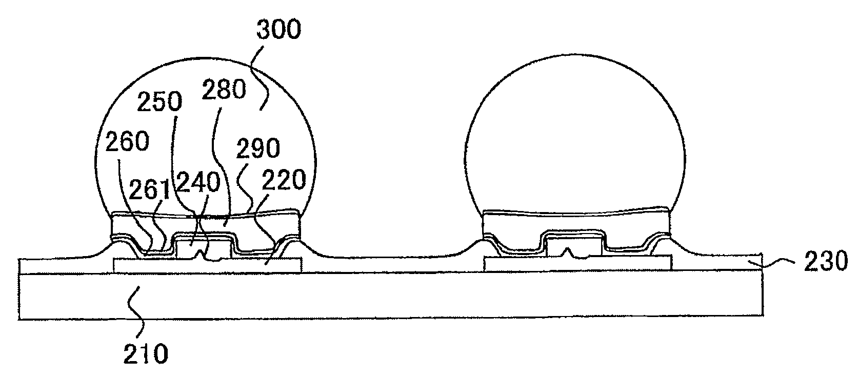
参照图2,在形成晶体管以及多层布线(图中未示出)的半导体基板210的表面的周边缘部,用电子束蒸镀法或喷溅法形成铝膜,通过将其制作成图案而形成衬垫电极220。然后,在前述衬垫电极220上,按照覆盖衬垫电极220的方式,形成成为保护膜的氮化硅膜230,并且,在前述保护膜230中,按照露出前述衬垫电极220的方式,形成开口部。Referring to FIG. 2, an aluminum film is formed by an electron beam evaporation method or a sputtering method on the peripheral portion of the surface of a
B.半导体装置的探针检查工序B.Probe inspection process of semiconductor devices
形成图2所示的结构之后,图3的工序中,为确认电气信号,进行探针检查。After forming the structure shown in FIG. 2 , in the process of FIG. 3 , probe inspection is performed to confirm electrical signals.
其结果,如图3所示,在前述探针检查之后,在衬垫电极220上,由于探针碰压而残留凹凸状的压痕的探针痕240(以下称为探针痕)。As a result, as shown in FIG. 3 , probe marks 240 (hereinafter referred to as probe marks) of concave and convex impressions remain on the
C.衬垫电极表面的探针痕上形成氮化硅膜的工序C. Step of forming a silicon nitride film on the probe marks on the pad electrode surface
进而,图4的工序中,在图3的结构上,按照覆盖探针痕240的方式,形成氮化硅膜等的膜,进一步,将其形成图案,并与前述探针痕240对应地形成覆盖前述探针痕240的氮化硅膜250。Furthermore, in the process of FIG. 4, a film such as a silicon nitride film is formed on the structure of FIG. A
D:Ti层和Cu层的形成工序D: Formation process of Ti layer and Cu layer
接下来,图5的工序中,在图4的结构之上,按照覆盖前述衬垫电极220和氮化硅膜250的方式,利用喷溅法,依次形成厚度分别为300nm和200nm的Ti层260和Cu层261。Next, in the process of FIG. 5, Ti layers 260 with thicknesses of 300 nm and 200 nm are sequentially formed on the structure of FIG. and
E.抗蚀膜的形成图案工序E. Patterning process of resist film
接着,图6的工序中,在图5的结构上形成抗蚀膜270,将其按照覆盖衬垫电极220以外的区域的方式形成图案。Next, in the step of FIG. 6 , a resist
F.Ni层和Au层的形成工序F. Formation process of Ni layer and Au layer
然后,图7的工序中,在图6的结构上,利用电镀法形成4000nm厚度的Ni层280,进一步,在Ni层280上作为氧化防止膜形成200nm厚度的Au层290。Next, in the process of FIG. 7, a
G.抗蚀膜的除去工序G. Removal process of resist film
接着,图8工序中,执行灰化处理,除去图7的抗蚀膜270。Next, in the step of FIG. 8 , ashing treatment is performed to remove the resist
H.Ti层和Cu层的蚀刻工序H. Etching process of Ti layer and Cu layer
下面,图9的工序中,将衬垫电极220上形成的Ni层280和Au层290用掩模盖住,将衬垫电极220以外的区域所形成的Ti层260和Cu层261通过蚀刻或者离子蚀刻而除去。Next, in the process of FIG. 9, the
I.凸块的形成工序I. Bump formation process
进而,图10的工序中,在Au层290上,通过印刷法、复制法、电镀法之中的任意一个方法,形成由Sn-Ag系合金形成的无铅焊锡或者由Sn-Pb系合金形成的铅焊锡。之后,对前述焊锡进行热处理,而形成凸块电极300。Furthermore, in the process of FIG. 10, on the
然而,本实施例子中,按照覆盖衬垫电极220表面的探针痕240的方式,形成保护膜、例如无机膜的氮化硅膜图案250,由此在衬垫电极220上,按照覆盖前述氮化硅膜图案250的方式,能够连续地形成Ti层260和Cu层261,所以在前述衬垫电极220上,通过电镀法连续地形成Ni图案280或者Au图案290,使得与前述衬垫电极220对应的区域能够一样地被覆盖,其结果即使形成了凸块电极300,在其下面不会形成如现有的空洞。在前述粘合层260、261和衬垫电极220之间形成氮化硅膜250,对于衬垫电极220上有压痕的情况,例如存在探针痕的情况,是非常有效的。However, in this embodiment example, a protective film, such as an inorganic silicon
此外,本实施例中,前述保护膜图案250是氮化硅膜等的绝缘膜,但本发明并不限定于此,也可以将氧化硅膜等的其它绝缘膜,或者聚酰亚胺树脂等的有机膜,或者金属或合金等的导电膜作为保护膜图案250而使用。例如,替代前述保护膜图案250,而形成作为导电性的膜的糊状的Ag、Pt、Pd、Cu之中任意一种也都能得到同样的效果。In addition, in this embodiment, the above-mentioned
[第2实施例][Second embodiment]
图11~14是表示根据本发明的第2实施方式的半导体装置的制造工序的图。但是,图中与先前说明过的部分对应的部分,赋予同一的参照符号,省略说明。11 to 14 are diagrams showing manufacturing steps of the semiconductor device according to the second embodiment of the present invention. However, in the drawings, parts corresponding to those described above are assigned the same reference numerals, and description thereof will be omitted.
A.半导体装置的探针检查工序A.Probe inspection process of semiconductor devices
如图11所示,在半导体基板210上,形成衬垫电极220和基板保护膜230以后进行的探针检查的结果,衬垫电极220表面的凹凸状的压痕作为探针痕240而残留。As shown in FIG. 11 , as a result of probe inspection performed after forming
B.利用干刻法的探针痕的平坦化工序B. Planarization process of probe marks by dry etching
接下来,如图12所示,以前述衬垫电极220的表面上包含探针痕240的方式进行干刻,平坦化探针痕240。Next, as shown in FIG. 12 , dry etching is performed so that the probe marks 240 are included on the surface of the
C.Ti层和Cu层的形成工序C. Formation process of Ti layer and Cu layer
下面,图13的工序中,在图12的结构上,利用喷溅法,按照覆盖前述基板保护膜230及衬垫电极220的方式,依次形成厚度分别为300nm和200nm的Ti层260和Cu层261。Next, in the process of FIG. 13 , on the structure of FIG. 12 , a
D.凸块的形成工序D. Bump forming process
之后,经过实施例1的图6~9所示的工序后,如图14所示,在衬垫电极220上的Cu层261的上面,Ni层280以4000nm的厚度,此外Au层290以200nm的厚度形成,进而,通过形成Sn-Ag系无铅合金焊锡或者是Sn-Pb系的铅合金焊锡,并进行热处理,而形成凸块电极300。Afterwards, after the steps shown in FIGS. 6 to 9 of Example 1, as shown in FIG. 14 , on the
这样,本实施方式中,将探针痕240的凹凸阶差通过平坦化而减小,从而能够使Ti层260以及Cu层261在衬垫电极220上连续地、一样地形成,在不产生空洞的情况下能够形成凸块电极300。In this way, in this embodiment, the unevenness of the probe marks 240 is reduced by flattening, so that the
此外,本实施例中,探针痕240的平坦化是利用干刻法进行的,但用湿刻法来代替也能得到同样的效果。另外,代替干刻法,也可以将衬垫电极220在600~800℃的温度下熔解来进行探针痕240的平坦化处理。进一步,代替干刻法,对于探针痕240施加机械压力,使用物理方法将探针痕240平坦化,也能得到同样的效果。In addition, in this embodiment, the planarization of the probe marks 240 is performed by dry etching, but the same effect can be obtained by using wet etching instead. In addition, instead of the dry etching method, the
[第3实施例][third embodiment]
图15~16是表示根据本发明的第3实施方式的半导体装置的制造工序的图。但在图中,与先前说明过的部分对应的部分赋予同一参照符号,省略说明。15 to 16 are views showing the manufacturing process of the semiconductor device according to the third embodiment of the present invention. However, in the drawings, the parts corresponding to the parts described above are given the same reference numerals, and the description thereof will be omitted.
参照图15,本实施例中,在探针检查之后,按照覆盖探针痕240的形成后的衬垫电极220以及钝化膜230的方式,利用喷溅法,以比先前的实施例更厚的,例如500nm的膜厚依次形成Ti层262和Cu层263。Referring to FIG. 15 , in this embodiment, after the probe inspection, the formed
然后,经过先前图6~9所示的工序后,如图16所示,在衬垫电极220上的Cu层263的上面,Ni层280以4000nm的厚度,此外Au层以200nm的厚度通过电镀法形成,进而,形成由Sn-Ag系合金形成的无铅焊锡,或者由Sn-Pb系合金形成的铅焊锡。之后,对前述合金焊锡进行热处理,形成凸块300电极。Then, after the previous steps shown in FIGS. 6 to 9, as shown in FIG. 16, on the
本实施方式中,这样地,使Ti层262和Cu层263厚些,最好与前述探针痕240的阶差相等,或者超过此的例如1um的程度的厚度来形成,从而探针痕240的凹凸状的阶差相对就变小,或者变得能够无视了,能够将前述Ti层262和Cu层263在前述衬垫电极220上连续形成。In this embodiment, in this way, the
此外,以上的各实施方式中,粘合层260并不限定于Ti层,也可以由Ti、Cr、TiW、Mo、Ta、W、Nb、V之中的任意一种来构成。另外,前述电极层261并不限定于Cu,也可以是Ni、Cu、Pd、Pt、Au、Ag之中的任意一种来构成。进一步,形成这些的过程并不限定于喷溅法,也能由蒸镀法或者MOCVD法来形成。In addition, in each of the above embodiments, the
另外,成为前述凸块的基底层(UBM层:under bump metal)的导电层280并不限定于Ni层,也可以由含有Ni、Cu的合金来构成。此外,前述氧化防止膜290并不限定于Au,也可以由Pt、Pd、In之中的任意一种来形成。In addition, the
并且,前述凸块电极300并不限定于Sn-Ag合金或者Pb-Sn合金,也可以是Pd、Ni、Cu、Sn及Pb的合金,或者是Au、Ag。In addition, the
以上详细记述了本发明的优选实施例,但本发明并不限定于相关的特定的实施方式,在权力要求书所述的本发明的要旨的范围内的各种变形、变更也是可能的。Preferred embodiments of the present invention have been described in detail above, but the present invention is not limited to the specific embodiments concerned, and various modifications and changes are possible within the scope of the present invention described in the claims.
根据本发明,基板上形成的衬垫电极即使有凹凸状的压痕,也可以在其上面稳定地连续形成导电膜,通过将这样的导电膜对电极进行电镀,可在衬垫电极的整个面形成导电层。其结果,在这样的导电层上,稳定地不产生空洞的形成而形成凸块电极。According to the present invention, even if the pad electrodes formed on the substrate have concavo-convex indentations, a conductive film can be stably and continuously formed thereon. Form a conductive layer. As a result, bump electrodes are stably formed on such a conductive layer without formation of voids.
根据本发明,探针电极所接触的衬垫电极上也可以形成凸块电极,因此不需要另外形成测试用的凸块电极,可有效地利用基板表面,从而可将半导体装置微细化。According to the present invention, bump electrodes can also be formed on the pad electrodes contacted by the probe electrodes. Therefore, it is not necessary to separately form bump electrodes for testing, and the surface of the substrate can be effectively used to miniaturize the semiconductor device.
Claims (6)
Applications Claiming Priority (1)
| Application Number | Priority Date | Filing Date | Title |
|---|---|---|---|
| PCT/JP2002/006245 WO2004001839A1 (en) | 2002-06-21 | 2002-06-21 | Semiconductor device and its producing method |
Related Parent Applications (1)
| Application Number | Title | Priority Date | Filing Date |
|---|---|---|---|
| CNB028291050A Division CN100382262C (en) | 2002-06-21 | 2002-06-21 | Semiconductor device and method for manufacturing the same |
Publications (2)
| Publication Number | Publication Date |
|---|---|
| CN101145533A CN101145533A (en) | 2008-03-19 |
| CN100536103C true CN100536103C (en) | 2009-09-02 |
Family
ID=29727367
Family Applications (2)
| Application Number | Title | Priority Date | Filing Date |
|---|---|---|---|
| CNB028291050A Expired - Fee Related CN100382262C (en) | 2002-06-21 | 2002-06-21 | Semiconductor device and method for manufacturing the same |
| CNB2007101807338A Expired - Fee Related CN100536103C (en) | 2002-06-21 | 2002-06-21 | Method of fabricating semiconductor device |
Family Applications Before (1)
| Application Number | Title | Priority Date | Filing Date |
|---|---|---|---|
| CNB028291050A Expired - Fee Related CN100382262C (en) | 2002-06-21 | 2002-06-21 | Semiconductor device and method for manufacturing the same |
Country Status (8)
| Country | Link |
|---|---|
| US (1) | US7095045B2 (en) |
| EP (1) | EP1517364B1 (en) |
| JP (1) | JP3978449B2 (en) |
| KR (1) | KR100643645B1 (en) |
| CN (2) | CN100382262C (en) |
| DE (1) | DE60239493D1 (en) |
| TW (1) | TW546841B (en) |
| WO (1) | WO2004001839A1 (en) |
Families Citing this family (20)
| Publication number | Priority date | Publication date | Assignee | Title |
|---|---|---|---|---|
| JP4213672B2 (en) * | 2003-04-15 | 2009-01-21 | 富士通マイクロエレクトロニクス株式会社 | Semiconductor device and manufacturing method thereof |
| TWI263856B (en) | 2004-11-22 | 2006-10-11 | Au Optronics Corp | IC chip, IC assembly and flat display |
| DE102005051857A1 (en) * | 2005-05-25 | 2007-02-22 | Fraunhofer-Gesellschaft zur Förderung der angewandten Forschung e.V. | UBM-PAD, solder contact and method of making a solder joint |
| JP4998270B2 (en) | 2005-12-27 | 2012-08-15 | 富士通セミコンダクター株式会社 | Semiconductor device and manufacturing method thereof |
| KR100859641B1 (en) * | 2006-02-20 | 2008-09-23 | 주식회사 네패스 | Semiconductor with solder bump with suppressing growth of inter-metallic compound and fabrication method thereof |
| JP5050384B2 (en) * | 2006-03-31 | 2012-10-17 | 富士通セミコンダクター株式会社 | Semiconductor device and manufacturing method thereof |
| JP5238206B2 (en) * | 2006-09-26 | 2013-07-17 | 株式会社フジクラ | Wiring board, electronic component and manufacturing method thereof |
| KR100857365B1 (en) * | 2007-02-28 | 2008-09-05 | 주식회사 네패스 | Bump structure of semiconductor device |
| CN101431037B (en) * | 2007-11-06 | 2011-03-30 | 宏茂微电子(上海)有限公司 | Manufacturing method of wafer level packaging structure |
| JP5627835B2 (en) * | 2007-11-16 | 2014-11-19 | ローム株式会社 | Semiconductor device and manufacturing method of semiconductor device |
| TWI394253B (en) * | 2009-03-25 | 2013-04-21 | 日月光半導體製造股份有限公司 | Package structure of bumped wafer and bumped wafer |
| JP2011165862A (en) * | 2010-02-09 | 2011-08-25 | Sony Corp | Semiconductor device, chip-on-chip mounting structure, method for manufacturing semiconductor device, and method for forming chip-on-chip mounting structure |
| US8492892B2 (en) | 2010-12-08 | 2013-07-23 | International Business Machines Corporation | Solder bump connections |
| US9941176B2 (en) * | 2012-05-21 | 2018-04-10 | Taiwan Semiconductor Manufacturing Company, Ltd. | Selective solder bump formation on wafer |
| US9537066B2 (en) * | 2013-07-30 | 2017-01-03 | Dowa Electronics Materials Co., Ltd. | Method of manufacturing semiconductor light emitting device, and semiconductor light emitting device |
| US8779604B1 (en) * | 2013-11-06 | 2014-07-15 | Chipmos Technologies Inc. | Semiconductor structure and manufacturing method thereof |
| JP6450560B2 (en) * | 2014-10-24 | 2019-01-09 | 新日本無線株式会社 | Semiconductor device and manufacturing method thereof |
| CN108962431B (en) * | 2017-05-23 | 2024-07-02 | 上海昊佰智造精密电子股份有限公司 | Single-layer conductive cloth and die cutting device for same |
| CN112366131B (en) * | 2020-10-21 | 2023-01-03 | 武汉新芯集成电路制造有限公司 | Method for manufacturing semiconductor device |
| CN115708203B (en) * | 2021-08-19 | 2025-08-01 | 长鑫存储技术有限公司 | Semiconductor structure and preparation method thereof |
Family Cites Families (13)
| Publication number | Priority date | Publication date | Assignee | Title |
|---|---|---|---|---|
| JPS61253847A (en) * | 1985-05-02 | 1986-11-11 | Nec Corp | Highly reliable semiconductor device |
| JPS63249346A (en) * | 1987-04-03 | 1988-10-17 | Fujitsu Ltd | Pad in integrated circuit chip and formation thereof |
| JPH01295444A (en) * | 1988-02-09 | 1989-11-29 | Fujitsu Ltd | Manufacture of semiconductor device |
| JPH06267884A (en) * | 1993-03-12 | 1994-09-22 | Mitsubishi Electric Corp | Method for manufacturing semiconductor device |
| KR100327442B1 (en) * | 1995-07-14 | 2002-06-29 | 구본준, 론 위라하디락사 | Bump Structure and Forming Method of Semiconductor Device |
| JP3756234B2 (en) * | 1996-02-22 | 2006-03-15 | ローム株式会社 | Semiconductor device including semiconductor chip and functional test trace repair method for the chip |
| JP3504421B2 (en) * | 1996-03-12 | 2004-03-08 | 株式会社ルネサステクノロジ | Semiconductor device |
| JP3335562B2 (en) * | 1997-08-20 | 2002-10-21 | 富士通株式会社 | Semiconductor chip connection bump forming method |
| JP3638085B2 (en) * | 1998-08-17 | 2005-04-13 | 富士通株式会社 | Semiconductor device |
| US6251694B1 (en) * | 1999-05-26 | 2001-06-26 | United Microelectronics Corp. | Method of testing and packaging a semiconductor chip |
| TW466655B (en) * | 2001-02-23 | 2001-12-01 | Megic Corp | Flip chip and the manufacturing process thereof |
| US6782895B2 (en) * | 2001-08-20 | 2004-08-31 | L'oreal, S.A. | Compositions comprising at least one hydroxide compound and at least one complexing agent, and methods for using the same |
| US6782897B2 (en) * | 2002-05-23 | 2004-08-31 | Taiwan Semiconductor Manufacturing Co., Ltd. | Method of protecting a passivation layer during solder bump formation |
-
2002
- 2002-06-21 CN CNB028291050A patent/CN100382262C/en not_active Expired - Fee Related
- 2002-06-21 DE DE60239493T patent/DE60239493D1/en not_active Expired - Lifetime
- 2002-06-21 KR KR1020047019063A patent/KR100643645B1/en not_active Expired - Fee Related
- 2002-06-21 EP EP02738780A patent/EP1517364B1/en not_active Expired - Lifetime
- 2002-06-21 WO PCT/JP2002/006245 patent/WO2004001839A1/en not_active Ceased
- 2002-06-21 JP JP2004515450A patent/JP3978449B2/en not_active Expired - Fee Related
- 2002-06-21 CN CNB2007101807338A patent/CN100536103C/en not_active Expired - Fee Related
- 2002-06-27 TW TW091114197A patent/TW546841B/en not_active IP Right Cessation
-
2004
- 2004-11-29 US US10/998,182 patent/US7095045B2/en not_active Expired - Fee Related
Also Published As
| Publication number | Publication date |
|---|---|
| EP1517364A4 (en) | 2006-06-07 |
| JPWO2004001839A1 (en) | 2005-10-27 |
| KR20040111695A (en) | 2004-12-31 |
| US7095045B2 (en) | 2006-08-22 |
| TW546841B (en) | 2003-08-11 |
| US20050151250A1 (en) | 2005-07-14 |
| EP1517364B1 (en) | 2011-03-16 |
| DE60239493D1 (en) | 2011-04-28 |
| WO2004001839A1 (en) | 2003-12-31 |
| KR100643645B1 (en) | 2006-11-10 |
| EP1517364A1 (en) | 2005-03-23 |
| CN101145533A (en) | 2008-03-19 |
| CN1628379A (en) | 2005-06-15 |
| JP3978449B2 (en) | 2007-09-19 |
| CN100382262C (en) | 2008-04-16 |
Similar Documents
| Publication | Publication Date | Title |
|---|---|---|
| CN100382262C (en) | Semiconductor device and method for manufacturing the same | |
| TW200919677A (en) | Substrate structure and semiconductor package using the same | |
| US7501311B2 (en) | Fabrication method of a wafer structure | |
| JPS6149819B2 (en) | ||
| JP2005116632A (en) | Semiconductor device manufacturing method and semiconductor device | |
| KR100614548B1 (en) | Fabrication method of wiring substrate for mounting semiconductor element and semiconductor device | |
| JP2007317979A (en) | Manufacturing method of semiconductor device | |
| JPH09213863A (en) | Lead frame manufacturing method | |
| JP2001257227A (en) | Method for manufacturing semiconductor device | |
| US20060017171A1 (en) | Formation method and structure of conductive bumps | |
| TWI273639B (en) | Etchant and method for forming bumps | |
| JP2000150518A (en) | Method for manufacturing semiconductor device | |
| JP2005109171A (en) | Semiconductor device and manufacturing method thereof | |
| JP3638085B2 (en) | Semiconductor device | |
| US20010038293A1 (en) | Projection electrode, its forming method and apparatus for testing an electronic component | |
| US20060180945A1 (en) | Forming a cap above a metal layer | |
| JPH0922912A (en) | Semiconductor device and manufacturing method thereof | |
| JP3573894B2 (en) | Semiconductor device and manufacturing method thereof | |
| JPH07201922A (en) | Method for forming solder bumps on a substrate | |
| JP4077666B2 (en) | Contact probe manufacturing method | |
| JP2721580B2 (en) | Method for manufacturing semiconductor device | |
| JPH10294318A (en) | Electronic components | |
| JP2001118957A (en) | Semiconductor device | |
| JPS6341238B2 (en) | ||
| JPH09129648A (en) | Semiconductor element and mounting method thereof |
Legal Events
| Date | Code | Title | Description |
|---|---|---|---|
| C06 | Publication | ||
| PB01 | Publication | ||
| C10 | Entry into substantive examination | ||
| SE01 | Entry into force of request for substantive examination | ||
| ASS | Succession or assignment of patent right |
Owner name: FUJITSU MICROELECTRONICS CO., LTD. Free format text: FORMER OWNER: FUJITSU LIMITED Effective date: 20081107 |
|
| C41 | Transfer of patent application or patent right or utility model | ||
| TA01 | Transfer of patent application right |
Effective date of registration: 20081107 Address after: Tokyo, Japan Applicant after: FUJITSU MICROELECTRONICS Ltd. Address before: Kawasaki, Kanagawa, Japan Applicant before: Fujitsu Ltd. |
|
| C14 | Grant of patent or utility model | ||
| GR01 | Patent grant | ||
| C56 | Change in the name or address of the patentee |
Owner name: FUJITSU SEMICONDUCTOR CO., LTD. Free format text: FORMER NAME: FUJITSU MICROELECTRON CO., LTD. |
|
| CP01 | Change in the name or title of a patent holder |
Address after: Japan's Kanagawa Prefecture Yokohama Patentee after: FUJITSU MICROELECTRONICS Ltd. Address before: Japan's Kanagawa Prefecture Yokohama Patentee before: Fujitsu Microelectronics Ltd. |
|
| CP02 | Change in the address of a patent holder |
Address after: Japan's Kanagawa Prefecture Yokohama Patentee after: FUJITSU MICROELECTRONICS Ltd. Address before: Tokyo, Japan Patentee before: Fujitsu Microelectronics Ltd. |
|
| ASS | Succession or assignment of patent right |
Owner name: SUOSI FUTURE CO., LTD. Free format text: FORMER OWNER: FUJITSU SEMICONDUCTOR CO., LTD. Effective date: 20150519 |
|
| C41 | Transfer of patent application or patent right or utility model | ||
| TR01 | Transfer of patent right |
Effective date of registration: 20150519 Address after: Kanagawa Patentee after: SOCIONEXT Inc. Address before: Yokohama City, Kanagawa Prefecture, Japan Patentee before: FUJITSU MICROELECTRONICS Ltd. |
|
| CF01 | Termination of patent right due to non-payment of annual fee | ||
| CF01 | Termination of patent right due to non-payment of annual fee |
Granted publication date: 20090902 Termination date: 20180621 |