Phase synchronization system
The present invention relates to a phase synchronization system for calibrating the phase of a basic operating clock of a central processing unit in a system comprising a plurality of central processing units which are excited by those basic operating clocks.
In a conventional system, such as a multiprocessor, a basic operation clock for activating each of the respective central processing units is generated by a common basic operation clock generator installed in each of the respective central processing units and is added to each of the respective central processing units to synchronize the respective central processing units with each other, and fig. 4 shows a structure of a clock generator circuit thereof. The basic operation clock generator 20 generates basic operation clocks for exciting the respective concerned central processing units 30 on the basis of the system clock supplied from the oscillator 1, and adds them to the respective concerned central processing units 30.
This structure is employed to reduce the size of the basic operation clock generator as a common part. However, as integrated circuit technology advances, factors defining physical dimensions tend to depend heavily not only on the magnitude of the logic, but also on the number of inputs and outputs. Since the basic operation clocks must be allocated to each of the relevant central processors in the structure illustrated in fig. 4, the number of output terminals of the basic operation clock generator is defined by the number of central processors 30 supplied to the basic operation clock, and thus a limit for downsizing the physical size of the basic operation clock generator 20 is defined. Thus, downsizing of the system is hindered and the cost thereof may be increased.
To overcome the countermeasures against these drawbacks, as an example, a basic operation clock generator is installed to each central processing unit as shown in fig. 5, and in the central processing unit 2 of fig. 5, for example, the basic operation clock generator 21 generates a basic operation clock for the central processing unit 22 on the basis of a system clock supplied from an oscillator, and adds this basic operation clock to the central processing unit 22. The same operations are performed in other central processing units.
In the structure shown in fig. 5, the basic operation clock generator only needs to supply the basic operation clock to the central processing unit in the central processing unit itself, and optimization of the central processing unit becomes possible. In addition, the reduction in the number of basic operating clock generator input and output terminals facilitates the reduction in system size and facilitates the use of very large scale integrated circuits in the system. Furthermore, this architecture is advantageous when assembling a multiprocessor system by building up multiple single processors, each with a central processing unit, or by increasing the number of single multiprocessor systems. Thus, it is possible to obtain a wide variety of a batch of computers with exactly the same hardware configuration.
However, when the structure shown in fig. 5 is used, phase synchronization between basic operation clocks is also problematic in order to achieve synchronization between the central processing units.
For example, in japanese unexamined patent publication No. 123911/84, a method of calibrating the phase of a basic operation clock having a plurality of devices which are included in a system and are excited by the basic operation clock having identical repetition periods (as shown in fig. 5) is described.
According to this technique, microprocessors, each placed relative to two devices, divide the clock frequency applied by a clock source and apply the bus clock to the associated devices. To synchronize the clock buses to each of the devices concerned, both clocks are applied to the same AND gate, and one of the microprocessors is not clocked so long as the AND gate outputs a timing error signal that one of the microprocessors cannot apply a divide to the clock supplied by the clock source. Thus, the bus clock of one of the microprocessors is delayed, while the phase relationship is shifted in turn. Finally, the phases of both bus clocks are calibrated to each other. However, when using this method, it is necessary to detect a phase difference of bus clocks between devices. Accordingly, the structure of the and circuit varies according to the number of devices forming the system. As the number of devices increases, and-gates tend to become complex. Because the phase relationship is shifted in sequence to achieve synchronization, synchronization tends to be time consuming when the bus clock is at low speed or sometimes happening from time to time.
It is an object of the present invention to provide an arrangement for fast synchronization of devices comprised in a system and for energizing the devices with a basic operating clock, irrespective of the number of devices comprised in the system.
According to the invention, the basic operation clock generator is installed to each of the relevant devices, and the basic operation clock generators of each of the relevant devices are connected in cascade. The basic operation clock generator of the previous stage generates a synchronization signal in response to each particular state of the basic operation clock, and adds the synchronization signal to the basic operation clock generator of the next stage, and the basic operation clock generator of the next stage establishes a start state in the basic operation clock by using the synchronization signal supplied from the basic operation clock generator as a control signal, whereby the basic operation clock phases of the respective devices are matched with each other.
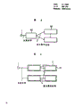
FIG. 1 is a block diagram of one embodiment of the present invention.
Fig. 2 shows the main part of fig. 1 in detail.
Fig. 3 is a timing chart explaining the operation of fig. 2.
Fig. 4 and 5 show structural examples of a common clock generator circuit.
An embodiment of the present invention will now be described with reference to fig. 1 to 3.
FIG. 1 is a block diagram of one embodiment of the present invention. In fig. 1, the invention is applied to a system comprising two central processing units.
The central processing unit 2 is composed of a basic operation clock generator 21 and a central processor 22. The basic operation clock generator 21 is composed of a basic clock generation circuit 211 for generating a basic clock for the basic operation clock generator 21 on the basis of a system clock of the oscillator 1, a basic operation clock generation circuit 212 for generating a basic operation clock on the basis of the basic clock, a synchronization signal generation circuit 213 for generating a synchronization signal for synchronizing the basic operation clock generator, a synchronization signal output terminal 215 for supplying a synchronization signal, a phase synchronization circuit 214 for establishing a special state in the basic clock generation circuit 211 on the basis of a control signal to be described later, and a control signal terminal 216 for receiving the control signal. In the same way, a central processing unit 3 is composed of a basic operation clock generator 31 and a central processor 32. The basic operation clock generator 31 is composed of a basic clock generation circuit 311, a basic operation clock generation circuit 312, a synchronization signal generation circuit 313, a synchronization signal output terminal 315, a phase synchronization circuit 314, and a control signal input terminal 316. Each of these processing components 2 and 3 may be comprised of one very large scale integrated circuit or may be comprised of separate units.
In the case shown in fig. 1, the basic operation clock generator 21 of the central processing unit 2 serves as a primary unit for achieving phase synchronization between the basic operation clocks, and the basic operation clock generator 31 of the central processing unit 3 serves as a secondary unit. I.e. the synchronization signal output 215 of the basic operation clock generator 21 at the primary part is connected to the control signal input 316 of the basic operation clock generator 31 at the secondary part. The synchronization signal generated by the synchronization signal generation circuit 213 is received by the phase synchronization circuit 314 of the secondary component as a control signal on the basis of the timing signal supplied from the basic clock generation circuit 211 of the primary component so as to establish a predetermined state in the basic clock generation circuit 311. By this operation, when the state of the basic clock generation circuit 311 at the main component and the state of the basic clock generation circuit 211 match, phase synchronization between the main and sub components is achieved. Until the output signal of the basic clock generation circuit 211 in the primary part is applied as a state-established signal to the basic clock generation circuit 311 of the secondary part, it passes through the wiring pattern connecting the synchronization signal generation circuit 311, the phase synchronization circuit 314, the synchronization signal output terminal 215, and the control signal input terminal 316. The sum of the delay times of these cells can be obtained when designing the corresponding cell. The state of the basic clock generation circuit 311 on the slave side is made to have a value of the calibration delay time.
In fig. 1, the basic operation clock generation circuits 212 and 312 constitute blocks separate from the synchronization signal generation circuits 213 and 313, respectively. However, it is obvious that both modules can be integrated without posing any problem. It is also apparent that such a structure in which the basic operation clock is used as a synchronization signal does not cause any problem. The same relationship corresponds to the phase synchronizing circuits 214 and 314 and the basic clock generating circuits 211 and 311, and also corresponds to the basic clock generating circuits 211 and 311 and the basic operation clock generating circuits 212 and 312. In the structure shown in fig. 1, the inputs of the synchronizing signal generating circuits 213 and 313 are taken out from the inputs of the basic operation clock generating circuits 212 and 312. However, for example, even if those inputs are taken from the outputs of the basic operation clock generation circuits 212 and 312, it is apparent that no problem is caused.
The operation of the embodiments of the present invention will be further described with reference to fig. 2 and 3. In fig. 2, the basic clock generation circuits 211 and 311 of the main and sub-components shown in fig. 1 are composed of four-bit counters 41 and 51, respectively. The main component synchronization signal generation circuit 213 is composed of an and gate 42. The phase synchronization circuit 314 of the secondary component is composed of an edge triggered bistable circuit 53. The four-bit calculators 41 and 51 are loop counters. Fig. 2 shows only the parts directly related to the narrative operation. The phase synchronization circuit 214 of the primary component, the synchronization signal generation circuit 313 of the secondary component, and the basic operation clock generation circuits 212 and 312 of the primary and secondary components, respectively, as shown in fig. 1, are omitted, and fig. 3 is a timing chart after phase synchronization is achieved to explain the operations of the respective parts of fig. 2.
The oscillator 1 transmits the system clock (fig. 3 (a)).
The four-bit counter 41 of the basic clock generation circuit 211 constituting the main component counts the system clock (fig. 3 (d)) supplied from the oscillator 1, as shown in fig. 3 (d). During the transfer between the oscillator and the basic clock generation circuit, the system clock is delayed by a time d due to the delay of the wiring. When the counter 41 counts to the value "14", the and gate 42 is structured to generate a pulse (synchronization signal), as shown in fig. 3 (e). The small circle at the input of AND gate 42 represents a negative logic operation. The synchronization signal generated in response to the count value "14" of the counter 41 is sent as a control signal to the phase synchronization circuit 314 of the secondary part, as shown in fig. 3 (f). During the transfer of the and gate 42 to the phase synchronizing circuit 53 of the secondary component, the synchronizing signal is delayed by a time D due to the delay of the device and the delay of the wiring. Since the delay time D does not exceed one system clock, the and gate 42 is configured to generate one pulse when the count reaches 14. In the case where the delay time D is equal to two system clocks, the and gate 42 is designed to generate one pulse when the count reaches 13.
The synchronization signal transmitted with such a delay time is then held, and is sent out when the counter 41 counts to "15", i.e., the delay time of one master clock. The signal generated in response to the count "15" of the counter 41 is applied to the load side of the four-bit counter 51 constituting the basic clock generation circuit 311 as a state establishment signal of the basic clock generation circuit 311 of the secondary component, as shown in fig. 3 (g). This state set-up signal is delayed, for example, by the delay of the device and the delay of the wiring. As a result, when the counter 41 counts to "0", the four-bit counter 51 of the basic clock generation circuit 311 constituting the secondary part is restored to the start value "0" at the data input terminals DO to D3 placed in the counter 51. The arrow of fig. 3 represents the instant at which counter 51 returns to "0".
When the count of the counter 41 of the primary part is "0", the counter 51 of the secondary part is also input with "0". Regardless of the value of the counter 51 of the secondary component before the arrow in fig. 3 (h), the primary component is synchronized with the secondary component at the instant indicated by the arrow. As soon as the synchronization signal is generated at the main component, the above-described synchronization operation is performed, and the rapidity of the synchronization lock is also ensured.
The system of fig. 1 comprises two central processing units 2 and 3. In the case of using three central processing units, the basic operation clock generator 31 of the central processing unit 3 is selected as a main unit, and a synchronization signal generated by its synchronization generating circuit 313 is applied to a phase synchronizing circuit of the basic operation clock generator included in the next-stage central processing unit through a terminal 315. Or the central processing unit 2 is selected as the main unit of the entire system, the synchronization signal generated by the synchronization signal generating circuit 213 is applied from the third unit to the phase synchronization circuit of the basic operation clock generator included in the central processing unit of the next several stages through the terminal 215 or in the same manner as the central processing unit 3, and of course, both methods may be combined, and any one of these methods may be applied to a system including any number of systems in the same manner. It is also apparent that the number of the synchronization signal generation circuits and the phase synchronization circuits need not coincide with the number of components supplied by the basic operation clock. That is, when the former method is used, the phase synchronization circuit of the first stage component and the synchronization signal generation circuit of the last stage component are not indispensable. When the post method is used, the phase synchronization circuit of the preceding stage or the main component and the synchronization signal generation circuit of the following stage or the sub component are not indispensable either.
In the above-described embodiment, the system clock generated by the oscillator 1 is added to the primary clock generation circuit 211 of the primary component and the primary clock generation circuit 311 of the secondary component after the same delay d. This is because the line length between the oscillator 1 and the basic clock generation circuit 211 is made equal to the line length between the oscillator 1 and the basic clock generation circuit 311.
As described above, the present invention makes it possible to quickly synchronize basic operation clocks of a plurality of components that are independently generated, and to use a circuit configuration that is independent of the number of components. Thus, the expansion of the unit can be realized easily at low cost.