CN102281702A - Substrate layout and its formation method - Google Patents
Substrate layout and its formation method Download PDFInfo
- Publication number
- CN102281702A CN102281702A CN2010105593895A CN201010559389A CN102281702A CN 102281702 A CN102281702 A CN 102281702A CN 2010105593895 A CN2010105593895 A CN 2010105593895A CN 201010559389 A CN201010559389 A CN 201010559389A CN 102281702 A CN102281702 A CN 102281702A
- Authority
- CN
- China
- Prior art keywords
- circuit
- ground plane
- circuit rail
- rail
- contact
- Prior art date
- Legal status (The legal status is an assumption and is not a legal conclusion. Google has not performed a legal analysis and makes no representation as to the accuracy of the status listed.)
- Granted
Links
Images




Classifications
-
- H—ELECTRICITY
- H10—SEMICONDUCTOR DEVICES; ELECTRIC SOLID-STATE DEVICES NOT OTHERWISE PROVIDED FOR
- H10W—GENERIC PACKAGES, INTERCONNECTIONS, CONNECTORS OR OTHER CONSTRUCTIONAL DETAILS OF DEVICES COVERED BY CLASS H10
- H10W70/00—Package substrates; Interposers; Redistribution layers [RDL]
- H10W70/60—Insulating or insulated package substrates; Interposers; Redistribution layers
- H10W70/62—Insulating or insulated package substrates; Interposers; Redistribution layers characterised by their interconnections
- H10W70/65—Shapes or dispositions of interconnections
-
- H—ELECTRICITY
- H05—ELECTRIC TECHNIQUES NOT OTHERWISE PROVIDED FOR
- H05K—PRINTED CIRCUITS; CASINGS OR CONSTRUCTIONAL DETAILS OF ELECTRIC APPARATUS; MANUFACTURE OF ASSEMBLAGES OF ELECTRICAL COMPONENTS
- H05K1/00—Printed circuits
- H05K1/02—Details
- H05K1/0213—Electrical arrangements not otherwise provided for
- H05K1/0237—High frequency adaptations
- H05K1/025—Impedance arrangements, e.g. impedance matching, reduction of parasitic impedance
- H05K1/0253—Impedance adaptations of transmission lines by special lay-out of power planes, e.g. providing openings
-
- H—ELECTRICITY
- H10—SEMICONDUCTOR DEVICES; ELECTRIC SOLID-STATE DEVICES NOT OTHERWISE PROVIDED FOR
- H10W—GENERIC PACKAGES, INTERCONNECTIONS, CONNECTORS OR OTHER CONSTRUCTIONAL DETAILS OF DEVICES COVERED BY CLASS H10
- H10W72/00—Interconnections or connectors in packages
-
- H—ELECTRICITY
- H05—ELECTRIC TECHNIQUES NOT OTHERWISE PROVIDED FOR
- H05K—PRINTED CIRCUITS; CASINGS OR CONSTRUCTIONAL DETAILS OF ELECTRIC APPARATUS; MANUFACTURE OF ASSEMBLAGES OF ELECTRICAL COMPONENTS
- H05K3/00—Apparatus or processes for manufacturing printed circuits
- H05K3/30—Assembling printed circuits with electric components, e.g. with resistors
- H05K3/32—Assembling printed circuits with electric components, e.g. with resistors electrically connecting electric components or wires to printed circuits
- H05K3/34—Assembling printed circuits with electric components, e.g. with resistors electrically connecting electric components or wires to printed circuits by soldering
- H05K3/341—Surface mounted components
- H05K3/3431—Leadless components
- H05K3/3436—Leadless components having an array of bottom contacts, e.g. pad grid array or ball grid array components
-
- H—ELECTRICITY
- H10—SEMICONDUCTOR DEVICES; ELECTRIC SOLID-STATE DEVICES NOT OTHERWISE PROVIDED FOR
- H10W—GENERIC PACKAGES, INTERCONNECTIONS, CONNECTORS OR OTHER CONSTRUCTIONAL DETAILS OF DEVICES COVERED BY CLASS H10
- H10W72/00—Interconnections or connectors in packages
- H10W72/071—Connecting or disconnecting
- H10W72/075—Connecting or disconnecting of bond wires
-
- H—ELECTRICITY
- H10—SEMICONDUCTOR DEVICES; ELECTRIC SOLID-STATE DEVICES NOT OTHERWISE PROVIDED FOR
- H10W—GENERIC PACKAGES, INTERCONNECTIONS, CONNECTORS OR OTHER CONSTRUCTIONAL DETAILS OF DEVICES COVERED BY CLASS H10
- H10W72/00—Interconnections or connectors in packages
- H10W72/30—Die-attach connectors
-
- H—ELECTRICITY
- H10—SEMICONDUCTOR DEVICES; ELECTRIC SOLID-STATE DEVICES NOT OTHERWISE PROVIDED FOR
- H10W—GENERIC PACKAGES, INTERCONNECTIONS, CONNECTORS OR OTHER CONSTRUCTIONAL DETAILS OF DEVICES COVERED BY CLASS H10
- H10W72/00—Interconnections or connectors in packages
- H10W72/851—Dispositions of multiple connectors or interconnections
- H10W72/874—On different surfaces
- H10W72/884—Die-attach connectors and bond wires
-
- H—ELECTRICITY
- H10—SEMICONDUCTOR DEVICES; ELECTRIC SOLID-STATE DEVICES NOT OTHERWISE PROVIDED FOR
- H10W—GENERIC PACKAGES, INTERCONNECTIONS, CONNECTORS OR OTHER CONSTRUCTIONAL DETAILS OF DEVICES COVERED BY CLASS H10
- H10W72/00—Interconnections or connectors in packages
- H10W72/90—Bond pads, in general
- H10W72/951—Materials of bond pads
- H10W72/952—Materials of bond pads comprising metals or metalloids, e.g. PbSn, Ag or Cu
-
- H—ELECTRICITY
- H10—SEMICONDUCTOR DEVICES; ELECTRIC SOLID-STATE DEVICES NOT OTHERWISE PROVIDED FOR
- H10W—GENERIC PACKAGES, INTERCONNECTIONS, CONNECTORS OR OTHER CONSTRUCTIONAL DETAILS OF DEVICES COVERED BY CLASS H10
- H10W90/00—Package configurations
- H10W90/701—Package configurations characterised by the relative positions of pads or connectors relative to package parts
- H10W90/731—Package configurations characterised by the relative positions of pads or connectors relative to package parts of die-attach connectors
- H10W90/734—Package configurations characterised by the relative positions of pads or connectors relative to package parts of die-attach connectors between a chip and a stacked insulating package substrate, interposer or RDL
-
- H—ELECTRICITY
- H10—SEMICONDUCTOR DEVICES; ELECTRIC SOLID-STATE DEVICES NOT OTHERWISE PROVIDED FOR
- H10W—GENERIC PACKAGES, INTERCONNECTIONS, CONNECTORS OR OTHER CONSTRUCTIONAL DETAILS OF DEVICES COVERED BY CLASS H10
- H10W90/00—Package configurations
- H10W90/701—Package configurations characterised by the relative positions of pads or connectors relative to package parts
- H10W90/751—Package configurations characterised by the relative positions of pads or connectors relative to package parts of bond wires
- H10W90/754—Package configurations characterised by the relative positions of pads or connectors relative to package parts of bond wires between a chip and a stacked insulating package substrate, interposer or RDL
-
- Y—GENERAL TAGGING OF NEW TECHNOLOGICAL DEVELOPMENTS; GENERAL TAGGING OF CROSS-SECTIONAL TECHNOLOGIES SPANNING OVER SEVERAL SECTIONS OF THE IPC; TECHNICAL SUBJECTS COVERED BY FORMER USPC CROSS-REFERENCE ART COLLECTIONS [XRACs] AND DIGESTS
- Y10—TECHNICAL SUBJECTS COVERED BY FORMER USPC
- Y10T—TECHNICAL SUBJECTS COVERED BY FORMER US CLASSIFICATION
- Y10T156/00—Adhesive bonding and miscellaneous chemical manufacture
- Y10T156/10—Methods of surface bonding and/or assembly therefor
- Y10T156/1089—Methods of surface bonding and/or assembly therefor of discrete laminae to single face of additional lamina
Landscapes
- Engineering & Computer Science (AREA)
- Microelectronics & Electronic Packaging (AREA)
- Structure Of Printed Boards (AREA)
- Physics & Mathematics (AREA)
- Geometry (AREA)
Abstract
Description
技术领域 technical field
本发明涉及封装基板与其制法,且为了达成电源完整性,特别是有关于一种具有可布线层(routable layer)的封装基板。The present invention relates to a package substrate and its manufacturing method, and in particular to a package substrate with a routable layer for achieving power integrity.
背景技术 Background technique
尽管已对集成电路或裸片进行封装(packaging),为了将裸片电性连接到其他外部元件或构件,一般而言,仍需要将裸片接合至一外部基板。于各种应用中,类似的基板,例如印刷电路板(printed circuit boards,PCB),已应用于半导体封装技术上。Although the integrated circuit or die has been packaged, in order to electrically connect the die to other external components or components, it is generally still necessary to bond the die to an external substrate. Similar substrates, such as printed circuit boards (PCBs), have been used in semiconductor packaging technology in various applications.
为了使基板上各层的使用效率达到最大化,单一层通常会包括一接地层(ground plane)作为第一电源回圈(first power loop)与一电源供应线路(powersupply trace)作为第二电源回圈(second power loop)。这些基板可包括多种不同的电源回圈,也可包括具有接地层与电源供应线路(power supply traces)的各种组合,位于基板的多层之上。然而,如何将接地层与电源供应线路设置于单一层上却可能带来问题,例如电源回圈的高阻抗(impedance)。In order to maximize the use efficiency of each layer on the substrate, a single layer usually includes a ground plane (ground plane) as the first power loop (first power loop) and a power supply trace (powersupply trace) as the second power loop Circle (second power loop). These substrates can include a variety of different power loops, as well as various combinations of ground planes and power supply traces, on multiple layers of the substrate. However, how to arrange the ground plane and the power supply line on a single layer may cause problems, such as high impedance of the power loop.
举例而言,于单一层的第一电源回圈中,一般的设置可包括一接地层,此接地层大体上围绕于裸片欲接合到基板的区域的两侧。一外层可包括球栅阵列(ball grid array,BGA),此球栅阵列具有电源供应连线(power supplyconnections)位于基板的外部边缘,其中介于所述多个连线与裸片区域之间的线用于切割开接地层。从这些连线连接到接地层的接触导通孔(vias)可将电源供应连线耦合到一线路(trace)。于一般的结构中,此线路(trace)将接地层切割成两等分,并且于接地层所在的两侧围绕着裸片区域。因此,此线路(trace)可具有”Y”型结构,其中裸片位于Y型上方分支(upper branches)之中与之间。因为线路(trace)可切断回流电流(return current)的直接路径(direct path),因而可避免在接地层中的回流电流沿着直接路径回流回来。换言之,回流电流因而转向(diverted),沿着该线路(trace)回流到耦合于裸片的接触导通孔(via)中。For example, in a single-layer first power loop, a typical arrangement may include a ground plane that generally surrounds both sides of the area where the die is to be bonded to the substrate. An outer layer may include a ball grid array (BGA) having power supply connections on an outer edge of the substrate between the plurality of connections and the die area The wire is used to cut open the ground plane. Contact vias from these connections to the ground plane can couple the power supply connection to a trace. In a typical configuration, this trace cuts the ground plane in half and surrounds the die area on both sides where the ground plane is located. Thus, the trace may have a "Y" structure with the die located in and between the upper branches of the Y. Since the trace can cut off the direct path of the return current, the return current in the ground plane can be prevented from flowing back along the direct path. In other words, the return current is thus diverted, flowing back along the trace into contact vias coupled to the die.
于上述的结构中,一般回流电流的转向(diversion)会增加电源回圈的阻抗(impedance)。于较高频率的条件下,阻抗的增加会更加显著。此外,也可能造成电源噪声(power noise)的增加,因而降低裸片中信号的真度(fidelity)。因此,需要提出一种基板布局(substrate layout)与其制法,此种布局能够降低或消除上述的缺点。In the above structure, generally the diversion of the return current will increase the impedance of the power loop. The increase in impedance is more pronounced at higher frequencies. In addition, it may also cause an increase in power noise, thereby reducing the fidelity of the signal in the die. Therefore, it is necessary to propose a substrate layout and its manufacturing method, which can reduce or eliminate the above-mentioned disadvantages.
发明内容 Contents of the invention
为克服上述现有技术的缺陷,本发明提供一种基板布局,包括:一第一电源回圈(first power loop)的一接地层(ground plane),位于一基板的一层上;一第一线路轨(first trace rail),位于该层上且沿着该接地层的一第一外围延伸,其中该接地层位于该第一线路轨与一裸片区域之间;以及一第一垂直线路(first perpendicular trace)耦合该第一线路轨,且从该第一线路轨垂直地延伸,其中该第一线路轨与该第一垂直线路组成一第二电源回圈。In order to overcome the defects of the above-mentioned prior art, the present invention provides a substrate layout, comprising: a ground plane of a first power loop (first power loop), located on one layer of a substrate; a first a first trace rail on the layer and extending along a first periphery of the ground layer, wherein the ground layer is between the first trace rail and a die area; and a first vertical trace ( The first vertical trace) is coupled to the first line track and extends vertically from the first line track, wherein the first line track and the first vertical line form a second power loop.
本发明另提供一种基板布局,包括:一接地层(ground plane),位于一基板的一层上,其中该接地层为一第一电源回圈(first power loop)的一部分;一第一线路轨(first trace rail),沿着该接地层的一第一外部边缘(first outer edge)延伸,其中该第一线路轨为一第二电源回圈的一部分,且该接地层位于该第一线路轨与一裸片区域之间;以及一第一线路(first trace)耦合该第一线路轨,其中该第二电源回圈中没有任何线路沿着垂直且与一回流电流(return current)的直接路径(direct path)相交叉(intersect)的方向延伸,其中该回流电流在该接地层中流到一回流电流结构,其中该回流电流结构大体上包含一接触导通孔(via)、一接触穿孔(through-via)或上述的组合。The present invention also provides a substrate layout, comprising: a ground plane (ground plane), located on a layer of a substrate, wherein the ground plane is a part of a first power loop (first power loop); a first line a first trace rail extending along a first outer edge of the ground plane, wherein the first trace rail is part of a second power loop, and the ground plane is located on the first line between the rail and a die area; and a first trace coupling the first trace, wherein none of the traces in the second power loop are along a direct path perpendicular to a return current. The direct path extends in an intersect direction, wherein the return current flows to a return current structure in the ground layer, wherein the return current structure generally includes a contact via (via), a contact through hole ( through-via) or a combination of the above.
本发明也提供一种基板布局的形成方法,包括以下步骤:提供具有一导电材料于其上的一基板,以该导电材料形成一接地层、一第一线路轨与一第一垂直线路,其中该第一线路轨沿着该接地层的一第一外部边缘延伸,且该第一垂直线路与该第一线路轨耦合并从该第一线路轨垂直地延伸,其中该接地层介于该第一线路轨与该基板的一区域间,其中该区域为后续裸片所在位置;以及形成一绝缘材料位于该接地层、该第一线路轨与该第一垂直线路之上。The present invention also provides a method for forming a substrate layout, including the following steps: providing a substrate with a conductive material thereon, using the conductive material to form a ground layer, a first line track and a first vertical line, wherein The first line track extends along a first outer edge of the ground plane, and the first vertical line is coupled to and extends perpendicularly from the first line track, wherein the ground plane is interposed between the first line track between a circuit track and an area of the substrate, wherein the area is where a subsequent die is located; and forming an insulating material on the ground layer, the first line track and the first vertical line.
本发明其中一项优点在于位于基板外部表面上的导电球的设置弹性,以及接触导通孔的设置弹性。另一优点在于位于接地层中的线路的设置弹性。垂直线路可设置于延伸穿过接地层的任何位置上。本发明阻抗的优于公知结构。One of the advantages of the present invention lies in the disposition flexibility of the conductive balls on the outer surface of the substrate and the disposition flexibility of the contact via holes. Another advantage resides in the flexibility of placement of the lines located in the ground plane. Vertical traces can be placed anywhere that extend through the ground plane. The impedance of the present invention is superior to that of known structures.
为让本发明的上述和其他目的、特征、和优点能更明显易懂,下文特举出优选实施例,并配合附图,作详细说明如下:In order to make the above-mentioned and other objects, features, and advantages of the present invention more clearly understood, the preferred embodiments are specifically listed below, together with the accompanying drawings, and are described in detail as follows:
附图说明 Description of drawings
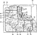
图1~图3为一系列俯视图,用以说明本发明各个实施例的基板的中间层。1 to 3 are a series of top views for illustrating intermediate layers of substrates according to various embodiments of the present invention.
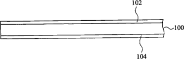
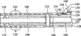
图4A~图4H为一系列剖面图,用以说明本发明一优选实施例制作基板的方法。4A-4H are a series of cross-sectional views for illustrating a method for fabricating a substrate according to a preferred embodiment of the present invention.
其中,附图标记说明如下:Wherein, the reference signs are explained as follows:
10~中间层10~middle layer
12、14~线路轨(trace rails)12, 14 ~ line rails (trace rails)
16、18、20、22~线路(trace)16, 18, 20, 22 ~ line (trace)
24、28、30~接触导通孔(vias)24, 28, 30~contact vias
26~接地层(ground plane)26~ground plane
32~裸片区域(die area)32~die area
40~中间层40~middle layer
42、44~线路轨(trace rails)42, 44~line rails (trace rails)
46、48、50、52~线路(trace)46, 48, 50, 52 to line (trace)
54、58、60~接触导通孔(vias)54, 58, 60~contact vias
56~接地层(ground plane)56~ground plane
62~裸片区域(die area)62~die area
70~中间层70~middle layer
72、74~线路轨(trace rails)72, 74~line rails (trace rails)
76、78、80、82~线路(trace)76, 78, 80, 82~Line (trace)
84、88、90~接触导通孔(vias)84, 88, 90~contact vias
86~接地层(ground plane)86~ground plane
92~裸片区域(die area)92~die area
100~核心100~core
102、104~金属导体(metal conductor)102, 104~metal conductor
106、108~接地层(ground planes)106, 108~ground planes
110、112、116~线路轨(rail traces)110, 112, 116 ~ rail traces
114、118~垂直线路114, 118~vertical lines
120、122~树脂(resin)120, 122 ~ resin (resin)
124~导通孔(via hole)124~via hole
126~金属导体126~metal conductor
128~穿孔(through-via hole)128~through-via hole
130~信号线(signal trace)130~signal trace
132~接触穿孔(through-via)132~contact perforation (through-via)
134~接触导通孔(via)134~contact via hole (via)
136、138~焊料掩模(solder mask)136, 138~solder mask (solder mask)
139~粘着层(adhesive)139~adhesive layer (adhesive)
140~裸片(die)140~bare chip (die)
142~镍142~nickel
146~导线(wire)146 ~ wire (wire)
148~裸片区域(die area)148~die area
具体实施方式 Detailed ways
以下特举出本发明的实施例,并配合附图作详细说明。以下实施例的元件和设计是为了简化所揭示的发明,并非用以限定本发明。Embodiments of the present invention are enumerated below and described in detail with accompanying drawings. The elements and designs of the following embodiments are for the purpose of simplifying the disclosed inventions, but are not intended to limit the present invention.
为了电性连接到集成电路或裸片,下述实施例涉及包含连线层的基板的特定内容。然而,也可应用到其他实施例的基板中(例如中介基板(interposersubstrate)),这些基板耦合到集成电路或裸片,。For electrical connection to an integrated circuit or die, the following embodiments refer to specific aspects of a substrate including a wiring layer. However, it is also applicable to other embodiments of substrates, such as interposer substrates, that are coupled to integrated circuits or die.
依据本发明的实施例,图1显示基板的中间层(intermediate layer)10。中间层(intermediate layer)10可以是基板中的任意一层。中间层10包含一“电源B(power B)”接地层26。图中也显示裸片区域32的轮廓,其中裸片可耦合到基板的外部表面。依图中所示,接地层26大体上围绕于裸片区域32的两侧。沿着裸片区域32的两侧为接触导通孔30,当裸片耦合到基板时,借由接触导通孔30使接地层26与裸片电性耦合。Figure 1 shows an intermediate layer 10 of a substrate according to an embodiment of the present invention. The intermediate layer (intermediate layer) 10 can be any layer in the substrate. The middle layer 10 includes a "power B" ground plane 26 . Also shown is the outline of a die area 32 where a die may be coupled to the exterior surface of the substrate. As shown in the figure, the ground layer 26 substantially surrounds two sides of the die area 32 . Along two sides of the die area 32 are contact vias 30 , through which the ground layer 26 is electrically coupled to the die when the die is coupled to the substrate.
线路轨(trace rails)12、14各自沿着接地层26的外部边缘(exterior edge)延伸,且接地层26介于线路轨12、14与裸片区域32之间。线路轨(trace rails)12、14为“电源A(power A)”回圈的一部分,且提供电源供应(power supply)与参考电压(reference voltage)。线路轨12沿着接地层26的边缘以第一方向延伸,而线路轨14沿着接地层26的另一边缘以第二方向延伸,此第二方向垂直于第一方向。线路轨12、14与接触导通孔(vias)24电性耦合,其中该接触导通孔24与位于基板外表面上的球栅阵列(ball grid array,BGA)焊接球电性耦合。BGA焊接球可位于与裸片相同或不同表面上。Trace rails 12 , 14 each extend along the exterior edge of ground plane 26 , and ground plane 26 is interposed between trace rails 12 , 14 and die area 32 . The trace rails 12, 14 are part of the "power A" loop and provide power supply and reference voltage. The line track 12 extends along an edge of the ground layer 26 in a first direction, and the line track 14 extends along another edge of the ground layer 26 in a second direction, and the second direction is perpendicular to the first direction. The circuit traces 12, 14 are electrically coupled to contact vias 24, wherein the contact vias 24 are electrically coupled to ball grid array (BGA) solder balls located on the outer surface of the substrate. BGA solder balls can be on the same or a different surface than the die.
第一、第二、第三、第四垂直线路16、18、20与22分别垂直地从各自的线路轨12、14延伸到接地层26中。垂直线路16、18、20与22为“电源A(power A)”回圈的另一部分,且其各自使线路轨12、14与接触导通孔28电性耦合,其中接触导通孔28与裸片电性耦合。垂直线路16、18、20与22各自垂直地延伸至最靠近自身线路的裸片区域32的边缘。须注意的是,线路轨12、14、垂直线路16、18、20、22皆与接地层26彼此电性隔离,使得线路轨12、14与垂直线路16、18、20、22不会短路(shorted),也不会与接地层26直接接触。The first, second, third and fourth vertical traces 16 , 18 , 20 and 22 respectively extend vertically from the respective traces 12 , 14 into the ground plane 26 . The vertical lines 16, 18, 20, and 22 are another part of the "power A (power A)" loop, and each electrically couples the line rails 12, 14 to the contact via 28, wherein the contact via 28 and the contact via 28 are electrically coupled to each other. The dies are electrically coupled. Vertical lines 16 , 18 , 20 and 22 each extend vertically to the edge of die area 32 closest to the line. It should be noted that the line tracks 12, 14, the vertical lines 16, 18, 20, 22 are electrically isolated from the ground layer 26, so that the line tracks 12, 14 and the vertical lines 16, 18, 20, 22 will not be short-circuited ( shorted), and will not be in direct contact with the ground plane 26.
于图1的结构中,流进接地层26的回流电流(return current)可更直接地(more directly)流到接触导通孔30,此接触导通孔30将回流电流导向裸片。由于垂直线路16、18、20、22皆从最接近自身的线路轨12或14和/或裸片区域的一侧垂直地延伸,因此,回流电流(return current)的直接路径(direct path)将不会受到“电源A”回圈中任何介于中间的线路所截断(cut off)。另言之,于接地层26中,仅有沿着接地层26的外部边缘而延伸的线路有可能沿着垂直于回流电流直接路径的方向延伸,除此之外,再也没有任何”电源A”线路垂直于回流电流(return current)的直接路径(direct path)。更精确地说,于此结构中,垂直线路16、18、20、22沿着平行于(parallel to)回流电流的直接路径的方向延伸。In the structure of FIG. 1, the return current flowing into the ground plane 26 can flow more directly to the contact via 30, which directs the return current to the die. Since the vertical lines 16, 18, 20, 22 all extend vertically from the side closest to their own line track 12 or 14 and/or the die area, the direct path of the return current (return current) will be Will not be cut off by any intervening lines in the "Power A" loop. In other words, in the ground layer 26, only the lines extending along the outer edge of the ground layer 26 may extend in a direction perpendicular to the direct path of the return current, and there is no other "power supply A" "The line is perpendicular to the direct path of the return current. More precisely, in this structure the vertical lines 16, 18, 20, 22 extend in a direction parallel to the direct path of the return current.
在此结构中,因为在“电源A”回圈中没有线路会切断接地层26中回流电流的直接路径,”电源B”回圈的阻抗(impedance)可因此降低,“电源A”回圈的阻抗也会降低。比起公知结构,可延长图1中“电源A”回圈中的线路,虽然这样做会增加线路的电阻(resistance),但发明人了解当考虑此结构的优点时,线路的增长并不会对电源回圈的阻抗造成不利的影响(adverselyeffect)。下述其他实施例将会更详细讨论此项观察结果。In this configuration, the impedance of the "Power B" loop can be reduced because there is no line in the "Power A" loop that would cut off the direct path of the return current in the ground plane 26, and the "Power A" loop's Impedance is also lowered. Compared with the known structure, the circuit in the "power supply A" loop in Fig. 1 can be extended, although doing so will increase the resistance of the circuit (resistance), but the inventor understands that when considering the advantages of this structure, the growth of the circuit does not It has an adverse effect on the impedance of the power loop. The other examples below discuss this observation in more detail.
依据本发明的另一实施例,图2显示基板的中间层40。图2中显示一“电源B(power B)”接地层56、一裸片区域62的轮廓,以及一接触导通孔60,当裸片耦合到基板时,接触导通孔60使接地层56与裸片电性耦合。如图中所示,接地层56大体上围绕于裸片区域62的两侧。According to another embodiment of the present invention, FIG. 2 shows an
线路轨(trace rails)42、44各自沿着接地层56的外部边缘(exterior edge)延伸,且接地层56介于线路轨42、44与裸片区域62之间。线路轨(trace rails)42、44为”电源A(power A)”回圈的一部分。线路轨42沿着接地层56的边缘以第一方向延伸,而线路轨44沿着接地层56的另一边缘以第二方向延伸,此第二方向垂直于第一方向。线路轨42、44与接触导通孔(vias)54电性耦合,其中该接触导通孔54与位于基板外表面上的球栅阵列(ball grid array,BGA)焊接球电性耦合。BGA焊接球可位于与裸片相同或不同表面上。Trace rails 42 , 44 each extend along the exterior edge of
类似于图1,第一、第二、第三、第四垂直线路46、48、50与52分别垂直地从各自的线路轨42、44延伸到接地层56中。垂直线路46、48、50与52为”电源A(power A)”回圈的另一部分,且其各自使线路轨42、44与接触导通孔58电性耦合,其中接触导通孔58与裸片电性耦合。垂直线路46、48、50与52各自垂直地延伸至最靠近自身线路的裸片区域62的边缘。Similar to FIG. 1 , first, second, third, and fourth
依据本发明的另一实施例,图3显示基板的中间层70。图3中显示一“电源B(power B)”接地层86、一裸片区域92的轮廓,以及一接触导通孔90,当裸片耦合到基板时,接触导通孔90使接地层86与裸片电性耦合。如图中所示,接地层86大体上围绕于裸片区域92的两侧。According to another embodiment of the present invention, FIG. 3 shows an
线路轨(trace rails)72、74各自沿着接地层86的外部边缘(exterior edge)延伸,且接地层86介于线路轨72、74与裸片区域92之间。线路轨(trace rails)72、74为“电源A(power A)”回圈的一部分。线路轨72沿着接地层86的边缘以第一方向延伸,而线路轨74沿着接地层86的另一边缘以第二方向延伸,此第二方向垂直于第一方向。线路轨72、74与接触导通孔(vias)84电性耦合,其中该接触导通孔84与位于基板外表面上的球栅阵列(ball grid array,BGA)焊接球电性耦合。BGA焊接球可位于与裸片的相同或不同表面上。Trace rails 72 , 74 each extend along the exterior edge of ground plane 86 , and ground plane 86 is interposed between trace rails 72 , 74 and die
类似于第1、2图,第一、第二、第三、第四垂直线路76、78、80与82分别垂直地从各自的线路轨72、74延伸到接地层86中。垂直线路76、78、80与82为”电源A(power A)”回圈的另一部分,且其各自使线路轨72、74与接触导通孔88电性耦合,其中接触导通孔88与裸片电性耦合。垂直线路76、78、80与82各自垂直地延伸至最靠近自身线路的裸片区域92的边缘。Similar to FIGS. 1 and 2, the first, second, third, and fourth
图1~图3的差异突显出这些实施例的优点。其中的一项优点在于位于基板外部表面上的导电球(conductive balls)的设置弹性(flexibility),以及接触导通孔(vias)的设置弹性。在图1~图3中的BGA球以及与BGA球电性耦合的接触导通孔24、54、84,可以以任意方式排列。如图1所示,接触导通孔24与BGA球位于靠近线路轨12、14的接点。如图2所示,3个接触导通孔54排列于垂直线路52上。如图3所示,2个接触导通孔84排列于垂直线路80上,且另一个接触导通孔84位于垂直线路78上。其他BGA球的设置以及与其电性耦合的接触导通孔的设置包括于其他实施例中,本发明的保护范围并不以所揭示的附图为限。此外,接触导通孔并不需要位于垂直线路上(垂直线路使线路轨与耦合至裸片上的接触导通孔耦合)。换言之,接触导通孔可与所述多个垂直导线分隔开,也可以借由另一线路与任一线路轨和/或垂直线路进行耦合。The differences in Figures 1-3 highlight the advantages of these embodiments. One of the advantages is the placement flexibility of the conductive balls on the outer surface of the substrate, as well as the placement flexibility of the contact vias. The BGA balls in FIGS. 1 to 3 and the contact via
另一优点在于位于接地层中的线路的设置弹性(flexibility)。垂直线路可设置于延伸穿过接地层的任何位置上。此外,垂直线路可直接与任何的线路轨耦合。须注意的是,此处所述的垂直线路垂直于线路轨或裸片区域边缘,或者平行于回流电流的直接路径。此处所使用的“垂直”和“平行”等用语,也包括依据一个基准线进行垂直或平行的次要路径变化(minor routingvariations),此次要路径变化基于避开穿孔的考虑或是生产基板的限制,目的在于防止线路(trace)垂直或平行,例如,于制作基板的过程中,导线只可延伸于四个方向中的某一方向(X方向、Y方向、与X方向相差正45度、与X方向相差负45度)Another advantage resides in the placement flexibility of the lines located in the ground plane. Vertical traces can be placed anywhere that extend through the ground plane. Additionally, vertical lines can be coupled directly to any line track. It should be noted that the vertical lines mentioned here are perpendicular to the line track or the edge of the die area, or parallel to the direct path of the return current. As used herein, the terms "perpendicular" and "parallel" also include minor routing variations that are perpendicular or parallel to a reference line based on considerations to avoid vias or to produce substrates. Restriction, the purpose is to prevent the line (trace) from being vertical or parallel. For example, in the process of making the substrate, the wire can only extend in one of the four directions (X direction, Y direction, plus 45 degrees from the X direction, minus 45 degrees from the X direction)
如上所述,上述实施例可同时降低电源A回圈与电源B回圈的阻抗。发明人也观察到图1~图3实施例的阻抗优于公知具有相对BGA配置的结构。由于降低上述情况中的阻抗,也可降低电源回圈中的噪声,或是降低存在于裸片中或从裸片输出的信号的噪声。As mentioned above, the above embodiments can simultaneously reduce the impedance of the power A loop and the power B loop. The inventors have also observed that the impedance of the embodiments of FIGS. 1-3 is superior to known structures with relative BGA configurations. As a result of reducing the impedance in the above case, it is also possible to reduce the noise in the power supply loop, or reduce the noise of the signal present in or output from the die.
关于图1的实施例,电源B回圈于频率266MHz、533MHz、800MHz的条件下的阻抗分别为0.74Ω、1.67Ω与2.88Ω,此数值分别高于公知结构67.5%、75.7%与89.5%。此外,此实施例中的电源A回圈于直流电(DC)的条件下具有0.08Ω的阻抗,此数值高于公知结构42.9%。Regarding the embodiment of FIG. 1 , the impedances of the power supply B loop at frequencies of 266MHz, 533MHz, and 800MHz are 0.74Ω, 1.67Ω, and 2.88Ω, respectively, which are 67.5%, 75.7%, and 89.5% higher than those of the conventional structure. In addition, the loop of the power supply A in this embodiment has an impedance of 0.08Ω under the condition of direct current (DC), which is 42.9% higher than that of the conventional structure.
关于图2的实施例,电源B回圈于频率266MHz、533MHz、800MHz的条件下的阻抗分别为0.76Ω、1.68Ω与2.70Ω,此数值分别高于公知结构69.0%、77.0%与97.7%。此外,此实施例中的电源A回圈于直流电(DC)的条件下具有0.09Ω的阻抗,此数值高于公知结构18.2%。Regarding the embodiment of FIG. 2 , the impedances of the power supply B loop at frequencies of 266MHz, 533MHz, and 800MHz are 0.76Ω, 1.68Ω, and 2.70Ω, respectively, which are 69.0%, 77.0%, and 97.7% higher than the conventional structure. In addition, the loop of the power supply A in this embodiment has an impedance of 0.09Ω under the condition of direct current (DC), which is 18.2% higher than that of the conventional structure.
关于图3之实施例,电源B回圈于频率266MHz、533MHz、800MHz的条件下之阻抗分别为0.79Ω、1.73Ω与2.86Ω,此数值分别高于公知结构68.4%、73.8%与85.6%。此外,此实施例中的电源A回圈于直流电(DC)的条件下具有0.06Ω的阻抗,此数值高于公知结构14.3%。Regarding the embodiment of FIG. 3 , the impedances of the power supply B loop at frequencies of 266MHz, 533MHz, and 800MHz are 0.79Ω, 1.73Ω, and 2.86Ω, respectively, which are 68.4%, 73.8%, and 85.6% higher than the known structure. In addition, the loop of the power source A in this embodiment has an impedance of 0.06Ω under the condition of direct current (DC), which is 14.3% higher than that of the conventional structure.
依据本发明的另一实施例,图4A-图4H显示基板的形成方法。于图4A中,提供一核心100,其中在核心100的上表面压合上一金属导体102,在核心100的下表面压合上另一金属导体104。金属导体102与104可以是铜。于图4B中,蚀刻金属导体102与104,以形成线路轨(rail traces)110、112与接地层106、108。图4B的剖面图的平面图显示于图4C中,其中沿着图4C中的线4B-4B以形成图4B的剖面。图4C中显示接地层106、线路轨110、116与垂直线路114、118。此布局为图1~图3的简化布局。此外,此布局所显示的是形成于核心100上表面的导线层(wiring layer),而且类似的布局可形成于核心100的下表面。According to another embodiment of the present invention, FIGS. 4A-4H show a method for forming a substrate. In FIG. 4A , a
于图4D中,形成树脂120以覆盖核心100上表面的导线层上,且形成另一树脂122以覆盖核心100下表面的导线层。于图4E中,蚀刻树脂120以形成导通孔(via hole)124,钻过树脂120、核心100与树脂122以形成穿孔(through-via hole)128。接着,电镀一金属导体126以覆盖整个结构。于第4F图中,蚀刻金属导体126以形成信号线130、接触穿孔132与接触导通孔134。形成一焊料掩模136以覆盖结构顶部,形成另一焊接掩模138以覆盖结构底部。In FIG. 4D , a
于图4G中,移除耦合到接触导通孔(via)134的金属导体上的焊料掩模(solder mask)136。接着,进行表面抛光(surface finish)。举例而言,于移除的区域电镀镍142与金144,以形成导线接合指状物(wire bond finger)。也可使用其他表面抛光步骤,例如使用无电极电镀镍金(electroless nickel immersiongold,ENIG)、无电极电镀镍钯金(nickel electroless palladium immersion gold,ENEPIG)或镍钯层。接着,裸片140借由粘着剂139接合到此结构。导线146用于接合指状物与裸片140,以形成结构与裸片之间的电性连接。图4H显示位于核心100上表面的金属线层,此图类似于第4C图。图4H中也显示迭加于(super-imposed)此布局上的接触穿孔(through-via)132、接触导通孔(via)与裸片区域148。In FIG. 4G ,
虽然本发明已以数个优选实施例揭示如上,然而其并非用以限定本发明,任何本领域技术人员,在不脱离本发明的精神和范围内,当可作任意的更动与润饰,因此本发明的保护范围当视随附的权利要求所界定的范围为准。Although the present invention has been disclosed above with several preferred embodiments, it is not intended to limit the present invention. Any skilled person in the art can make arbitrary changes and modifications without departing from the spirit and scope of the present invention. Therefore The protection scope of the present invention should be determined by the scope defined by the appended claims.
Claims (10)
Applications Claiming Priority (2)
| Application Number | Priority Date | Filing Date | Title |
|---|---|---|---|
| US12/814,102 US8289727B2 (en) | 2010-06-11 | 2010-06-11 | Package substrate |
| US12/814,102 | 2010-06-11 |
Publications (2)
| Publication Number | Publication Date |
|---|---|
| CN102281702A true CN102281702A (en) | 2011-12-14 |
| CN102281702B CN102281702B (en) | 2013-07-10 |
Family
ID=45096089
Family Applications (1)
| Application Number | Title | Priority Date | Filing Date |
|---|---|---|---|
| CN2010105593895A Active CN102281702B (en) | 2010-06-11 | 2010-11-23 | Substrate layout and forming method thereof |
Country Status (3)
| Country | Link |
|---|---|
| US (2) | US8289727B2 (en) |
| CN (1) | CN102281702B (en) |
| TW (1) | TWI424799B (en) |
Cited By (2)
| Publication number | Priority date | Publication date | Assignee | Title |
|---|---|---|---|---|
| CN104302103A (en) * | 2014-07-17 | 2015-01-21 | 威盛电子股份有限公司 | Circuit layout structure, circuit board and electronic assembly |
| CN104904326A (en) * | 2012-12-20 | 2015-09-09 | At&S奥地利科技与系统技术股份公司 | Semi-finished product for the production of a printed circuit board, method for producing a printed circuit board and printed circuit board |
Families Citing this family (8)
| Publication number | Priority date | Publication date | Assignee | Title |
|---|---|---|---|---|
| US9345132B2 (en) * | 2013-02-07 | 2016-05-17 | Global Unichip Corp. | Substrate structure and the process manufacturing the same |
| WO2015077808A1 (en) | 2013-11-27 | 2015-06-04 | At&S Austria Technologie & Systemtechnik Aktiengesellschaft | Circuit board structure |
| AT515101B1 (en) | 2013-12-12 | 2015-06-15 | Austria Tech & System Tech | Method for embedding a component in a printed circuit board |
| AT515447B1 (en) | 2014-02-27 | 2019-10-15 | At & S Austria Tech & Systemtechnik Ag | Method for contacting a component embedded in a printed circuit board and printed circuit board |
| US11523520B2 (en) | 2014-02-27 | 2022-12-06 | At&S Austria Technologie & Systemtechnik Aktiengesellschaft | Method for making contact with a component embedded in a printed circuit board |
| TWI543674B (en) * | 2014-07-17 | 2016-07-21 | 威盛電子股份有限公司 | Circuit layout structure, circuit board and electronic assembly |
| US11133254B2 (en) * | 2018-09-28 | 2021-09-28 | Taiwan Semiconductor Manufacturing Company, Ltd. | Hybrid power rail structure |
| TWI733454B (en) * | 2020-05-18 | 2021-07-11 | 矽品精密工業股份有限公司 | Electronic device, electronic package, and package substrate thereof |
Citations (2)
| Publication number | Priority date | Publication date | Assignee | Title |
|---|---|---|---|---|
| US5424492A (en) * | 1994-01-06 | 1995-06-13 | Dell Usa, L.P. | Optimal PCB routing methodology for high I/O density interconnect devices |
| CN2582211Y (en) * | 2002-08-12 | 2003-10-22 | 富士康(昆山)电脑接插件有限公司 | Electric connector |
Family Cites Families (31)
| Publication number | Priority date | Publication date | Assignee | Title |
|---|---|---|---|---|
| US4651417A (en) | 1984-10-23 | 1987-03-24 | New West Technology Corporation | Method for forming printed circuit board |
| JP2739726B2 (en) | 1990-09-27 | 1998-04-15 | インターナシヨナル・ビジネス・マシーンズ・コーポレーシヨン | Multilayer printed circuit board |
| US5153050A (en) * | 1991-08-27 | 1992-10-06 | Johnston James A | Component of printed circuit boards |
| US5268064A (en) * | 1992-02-04 | 1993-12-07 | Trimble Navigation Limited | Copper clad epoxy printed circuit board suitable for microwave frequencies encountered in GPS receivers |
| US5434750A (en) * | 1992-02-07 | 1995-07-18 | Lsi Logic Corporation | Partially-molded, PCB chip carrier package for certain non-square die shapes |
| JP3756580B2 (en) | 1995-11-07 | 2006-03-15 | セイコープレシジョン株式会社 | Multilayer substrate manufacturing method and manufacturing apparatus thereof |
| SG76530A1 (en) * | 1997-03-03 | 2000-11-21 | Hitachi Chemical Co Ltd | Circuit boards using heat resistant resin for adhesive layers |
| US5847936A (en) | 1997-06-20 | 1998-12-08 | Sun Microsystems, Inc. | Optimized routing scheme for an integrated circuit/printed circuit board |
| US6720501B1 (en) | 1998-04-14 | 2004-04-13 | Formfactor, Inc. | PC board having clustered blind vias |
| US6011695A (en) * | 1998-11-02 | 2000-01-04 | Intel Corporation | External bus interface printed circuit board routing for a ball grid array integrated circuit package |
| JP3669219B2 (en) | 1999-08-10 | 2005-07-06 | 日本電気株式会社 | Multilayer printed wiring board |
| JP4249360B2 (en) * | 1999-11-02 | 2009-04-02 | 日東電工株式会社 | Circuit board and manufacturing method thereof |
| US6404649B1 (en) | 2000-03-03 | 2002-06-11 | Advanced Micro Devices, Inc. | Printed circuit board assembly with improved bypass decoupling for BGA packages |
| KR100509058B1 (en) | 2000-04-11 | 2005-08-18 | 엘지전자 주식회사 | Making method of PCB |
| US6462423B1 (en) * | 2000-08-31 | 2002-10-08 | Micron Technology, Inc. | Flip-chip with matched lines and ground plane |
| US6710255B2 (en) * | 2001-03-30 | 2004-03-23 | Intel Corporation | Printed circuit board having buried intersignal capacitance and method of making |
| JP3840921B2 (en) | 2001-06-13 | 2006-11-01 | 株式会社デンソー | Printed circuit board and manufacturing method thereof |
| US6751113B2 (en) * | 2002-03-07 | 2004-06-15 | Netlist, Inc. | Arrangement of integrated circuits in a memory module |
| US7227254B2 (en) * | 2002-04-02 | 2007-06-05 | Agilent Technologies, Inc. | Integrated circuit package |
| US6804119B2 (en) * | 2002-07-31 | 2004-10-12 | Hewlett-Packard Development Company, L.P. | Method and edge connector providing electrostatic discharge arrest features and digital camera employing same |
| US7176383B2 (en) * | 2003-12-22 | 2007-02-13 | Endicott Interconnect Technologies, Inc. | Printed circuit board with low cross-talk noise |
| US6924712B2 (en) * | 2003-01-30 | 2005-08-02 | Broadcom Corporation | Semi-suspended coplanar waveguide on a printed circuit board |
| TWI264056B (en) * | 2005-05-27 | 2006-10-11 | Via Tech Inc | Ball grid array package substrate structure |
| USD574339S1 (en) * | 2005-06-24 | 2008-08-05 | Nitto Denko Corporation | Pattern formed on the ground layer of a multilayer printed circuit board |
| TWI286914B (en) * | 2005-07-29 | 2007-09-11 | Hon Hai Prec Ind Co Ltd | Printed circuit board having improved power regions |
| TW200720967A (en) * | 2005-11-30 | 2007-06-01 | Inventec Corp | Method of power/ground circuit wiring-aided for circuit layout |
| CN101048032A (en) * | 2006-03-29 | 2007-10-03 | 鸿富锦精密工业(深圳)有限公司 | Ground plane of printed circuit board |
| TWI340612B (en) * | 2007-07-24 | 2011-04-11 | Advanced Semiconductor Eng | Circuit substrate and method for fabricating inductive circuit |
| TWI358243B (en) * | 2008-08-27 | 2012-02-11 | Advanced Semiconductor Eng | Circuit substrate having power/ground plane with g |
| KR20100084379A (en) * | 2009-01-16 | 2010-07-26 | 삼성전자주식회사 | Printed circuit board |
| JP5995723B2 (en) * | 2009-11-06 | 2016-09-21 | モレックス エルエルシー | Multilayer circuit member having a reference circuit |
-
2010
- 2010-06-11 US US12/814,102 patent/US8289727B2/en active Active
- 2010-11-08 TW TW099138293A patent/TWI424799B/en active
- 2010-11-23 CN CN2010105593895A patent/CN102281702B/en active Active
-
2012
- 2012-09-14 US US13/620,225 patent/US9449909B2/en active Active
Patent Citations (2)
| Publication number | Priority date | Publication date | Assignee | Title |
|---|---|---|---|---|
| US5424492A (en) * | 1994-01-06 | 1995-06-13 | Dell Usa, L.P. | Optimal PCB routing methodology for high I/O density interconnect devices |
| CN2582211Y (en) * | 2002-08-12 | 2003-10-22 | 富士康(昆山)电脑接插件有限公司 | Electric connector |
Cited By (6)
| Publication number | Priority date | Publication date | Assignee | Title |
|---|---|---|---|---|
| CN104904326A (en) * | 2012-12-20 | 2015-09-09 | At&S奥地利科技与系统技术股份公司 | Semi-finished product for the production of a printed circuit board, method for producing a printed circuit board and printed circuit board |
| CN104904326B (en) * | 2012-12-20 | 2018-01-12 | At&S奥地利科技与系统技术股份公司 | For producing the semi-finished product, printed circuit board and its production method of printed circuit board |
| CN104302103A (en) * | 2014-07-17 | 2015-01-21 | 威盛电子股份有限公司 | Circuit layout structure, circuit board and electronic assembly |
| CN104302103B (en) * | 2014-07-17 | 2017-09-08 | 威盛电子股份有限公司 | Circuit layout structure, circuit board and electronic assembly |
| CN107529271A (en) * | 2014-07-17 | 2017-12-29 | 威盛电子股份有限公司 | Circuit layout structure, circuit board and electronic assembly |
| CN107529271B (en) * | 2014-07-17 | 2019-05-31 | 威盛电子股份有限公司 | Circuit layout structure, circuit board and electronic assembly |
Also Published As
| Publication number | Publication date |
|---|---|
| US9449909B2 (en) | 2016-09-20 |
| CN102281702B (en) | 2013-07-10 |
| US8289727B2 (en) | 2012-10-16 |
| TWI424799B (en) | 2014-01-21 |
| US20110304998A1 (en) | 2011-12-15 |
| TW201146107A (en) | 2011-12-16 |
| US20130015234A1 (en) | 2013-01-17 |
Similar Documents
| Publication | Publication Date | Title |
|---|---|---|
| CN102281702B (en) | Substrate layout and forming method thereof | |
| CN108140616B (en) | Semiconductor device with a plurality of transistors | |
| TWI536882B (en) | Printed circuit board with power/ground ball pad array | |
| JP5964957B2 (en) | Structure for high-speed signal integrity in a semiconductor package with a single metal layer substrate | |
| USRE49970E1 (en) | Manufacturing method and electronic module with new routing possibilities | |
| TWI572256B (en) | Circuit board and electronic assembly | |
| US20110147058A1 (en) | Electronic device and method of manufacturing electronic device | |
| CN100573858C (en) | chip package | |
| CN103889145B (en) | Circuit board and electronic assembly | |
| JP5190811B2 (en) | Power module | |
| US9078352B2 (en) | Low inductance flex bond with low thermal resistance | |
| TWI566352B (en) | Package substrate and package | |
| CN100539102C (en) | Electric connection structure with semiconductor chip embedded in circuit board | |
| TWI245380B (en) | Semiconductor device | |
| JP2011187683A (en) | Wiring board and semiconductor device | |
| CN201594536U (en) | Chip Stack Circuit Structure | |
| US10332863B2 (en) | Method of miniaturized chip on chip interconnection of a 3D electronic module | |
| JP2020013917A (en) | Wiring board | |
| JP2012248877A (en) | Semiconductor package having low speed and high speed signal paths | |
| CN100386873C (en) | wire bond package | |
| KR20140047877A (en) | Printed circuit boards and manufacturing methods thereof | |
| KR20190093482A (en) | Semiconductor package and method of fabricating the same | |
| JP7412305B2 (en) | Package substrate and package substrate manufacturing method | |
| JP4099072B2 (en) | Built-in module | |
| JP2008078314A (en) | High-speed signal circuit device |
Legal Events
| Date | Code | Title | Description |
|---|---|---|---|
| C06 | Publication | ||
| PB01 | Publication | ||
| C10 | Entry into substantive examination | ||
| SE01 | Entry into force of request for substantive examination | ||
| C14 | Grant of patent or utility model | ||
| GR01 | Patent grant |